Embed Size (px)
Citation preview
CS 433 Prof. Luddy Harrison Copyright 2005 University of Illinois 1
Analog Devices SHARC
CS 433Processor Presentation Series
Prof. Luddy Harrison
CS 433 Prof. Luddy Harrison Copyright 2005 University of Illinois 2
Note on this presentation series
These slide presentations were prepared by students of CS433 at the University of Illinois at Urbana-ChampaignAll the drawings and figures in these slides were drawn by the students. Some drawings are based on figures in the manufacturer’s documentation for the processor, but none are electronic copies of such drawingsYou are free to use these slides provided that you leave the credits and copyright notices intact
CS 433 Prof. Luddy Harrison Copyright 2005 University of Illinois 3
Overview
Processor HistoryPhysical packagingData paths, register files, computational unitsPipelining, timing informationMemoryInstruction Set Architecture (ISA)Applications targetedSystems employing the SHARC
CS 433 Prof. Luddy Harrison Copyright 2005 University of Illinois 4
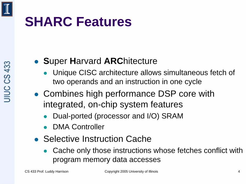
SHARC Features
Super Harvard ARChitectureUnique CISC architecture allows simultaneous fetch of two operands and an instruction in one cycle
Combines high performance DSP core with integrated, on-chip system features
Dual-ported (processor and I/O) SRAM DMA Controller
Selective Instruction CacheCache only those instructions whose fetches conflict with program memory data accesses
CS 433 Prof. Luddy Harrison Copyright 2005 University of Illinois 5
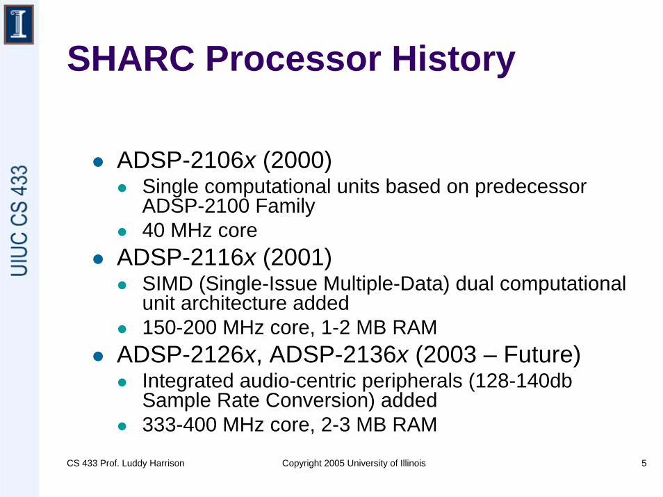
SHARC Processor History
ADSP-2106x (2000)Single computational units based on predecessor ADSP-2100 Family40 MHz core
ADSP-2116x (2001)SIMD (Single-Issue Multiple-Data) dual computational unit architecture added150-200 MHz core, 1-2 MB RAM
ADSP-2126x, ADSP-2136x (2003 – Future)Integrated audio-centric peripherals (128-140db Sample Rate Conversion) added333-400 MHz core, 2-3 MB RAM
CS 433 Prof. Luddy Harrison Copyright 2005 University of Illinois 6
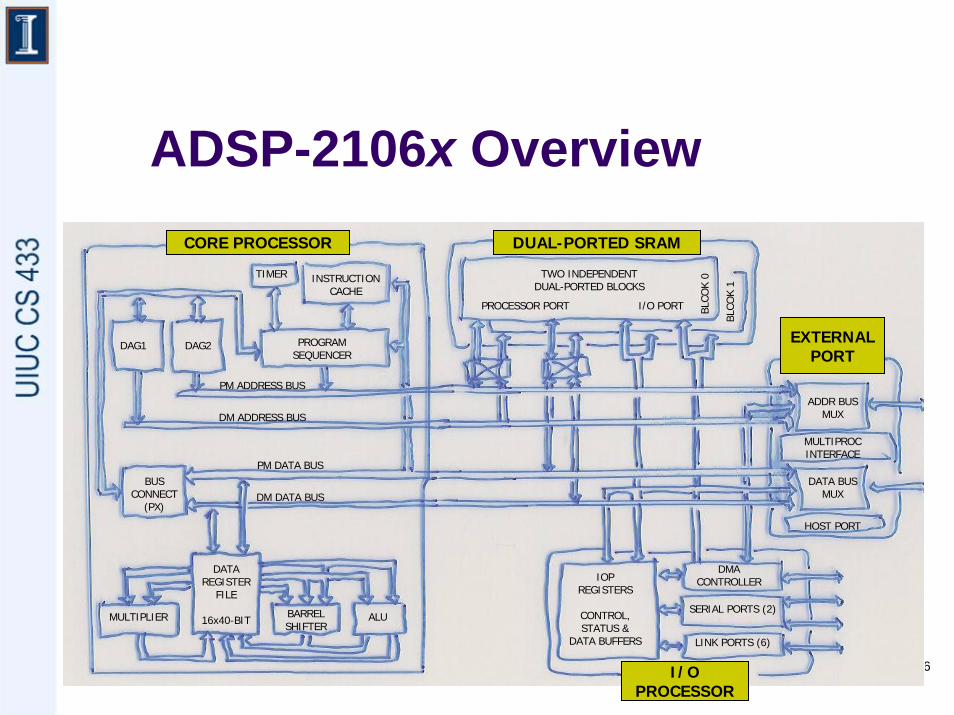
ADSP-2106x OverviewCORE PROCESSOR DUAL-PORTED SRAM
TIMER INSTRUCTION CACHE
PROGRAMSEQUENCER
DAG2DAG1
BUSCONNECT
(PX)
DATAREGISTER
FILE
16x40-BITMULTIPLIER BARRELSHIFTER
ALU
PM DATA BUS
DM DATA BUS
PM ADDRESS BUS
DM ADDRESS BUS
TWO INDEPENDENTDUAL-PORTED BLOCKS
PROCESSOR PORT I/O PORT BLCO
K 0
BLCO
K 1
EXTERNALPORT
ADDR BUSMUX
MULTIPROCINTERFACE
DATA BUSMUX
HOST PORT
IOPREGISTERS
CONTROL,STATUS &
DATA BUFFERS
DMACONTROLLER
SERIAL PORTS (2)
LINK PORTS (6)
I/OPROCESSOR
CS 433 Prof. Luddy Harrison Copyright 2005 University of Illinois 7
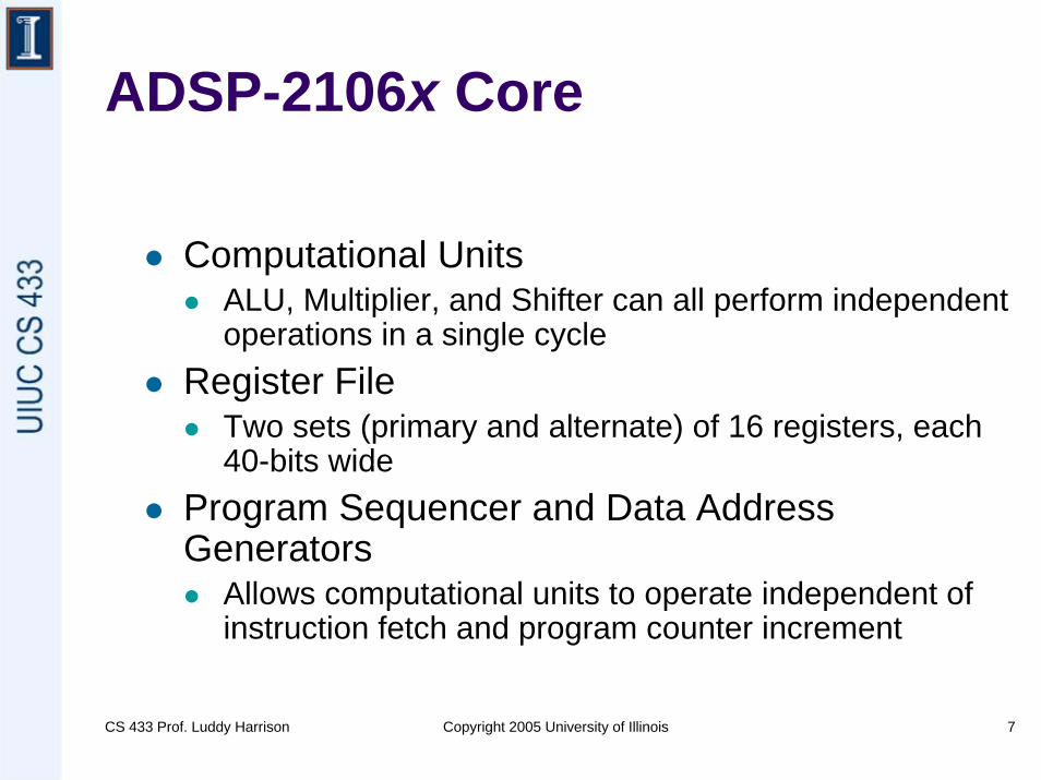
ADSP-2106x Core
Computational UnitsALU, Multiplier, and Shifter can all perform independent operations in a single cycle
Register FileTwo sets (primary and alternate) of 16 registers, each 40-bits wide
Program Sequencer and Data Address Generators
Allows computational units to operate independent of instruction fetch and program counter increment
CS 433 Prof. Luddy Harrison Copyright 2005 University of Illinois 8
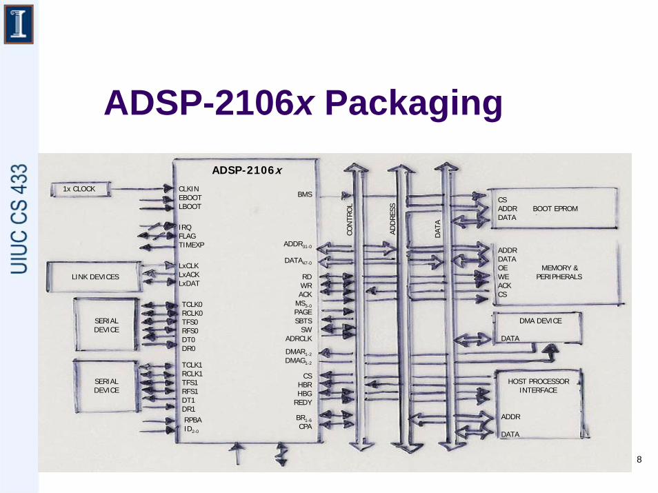
ADSP-2106x PackagingADSP-2106x
CLKINEBOOTLBOOT
IRQFLAGTIMEXP
LxCLKLxACKLxDAT
TCLK0RCLK0TFS0RFS0DT0DR0
TCLK1RCLK1TFS1RFS1DT1DR1
LINK DEVICES
SERIALDEVICE
SERIALDEVICE
1x CLOCKBMS
ADDR31-0
DATA47-0
RDWRACK
MS3-0PAGESBTS
SWADRCLK
DMAR1-2DMAG1-2
CSHBRHBG
REDY
BR1-6CPA
RPBAID2-0
CON
TRO
L
ADD
RES
S
DAT
A
CSADDR BOOT EPROMDATA
ADDRDATAOE MEMORY &WE PERIPHERALSACKCS
DMA DEVICE
DATA
HOST PROCESSORINTERFACE
ADDR
DATA
CS 433 Prof. Luddy Harrison Copyright 2005 University of Illinois 9
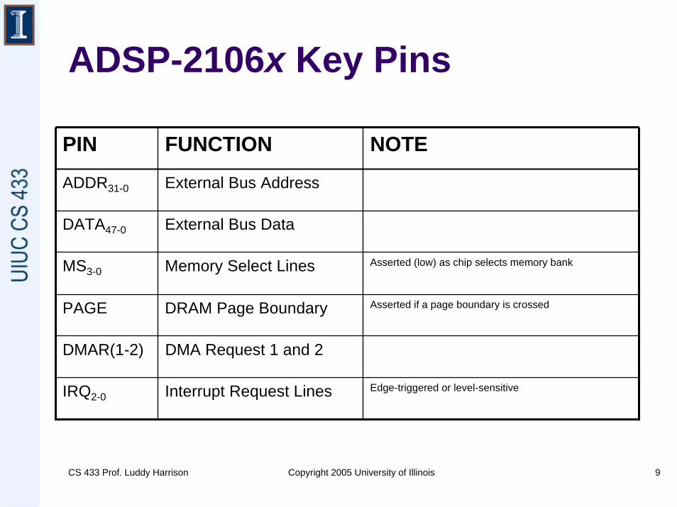
ADSP-2106x Key Pins
PIN FUNCTION NOTE
ADDR31-0 External Bus Address
DATA47-0 External Bus Data
Memory Select Lines
PAGE DRAM Page Boundary Asserted if a page boundary is crossed
DMAR(1-2) DMA Request 1 and 2
IRQ2-0 Interrupt Request Lines Edge-triggered or level-sensitive
MS3-0Asserted (low) as chip selects memory bank
CS 433 Prof. Luddy Harrison Copyright 2005 University of Illinois 10
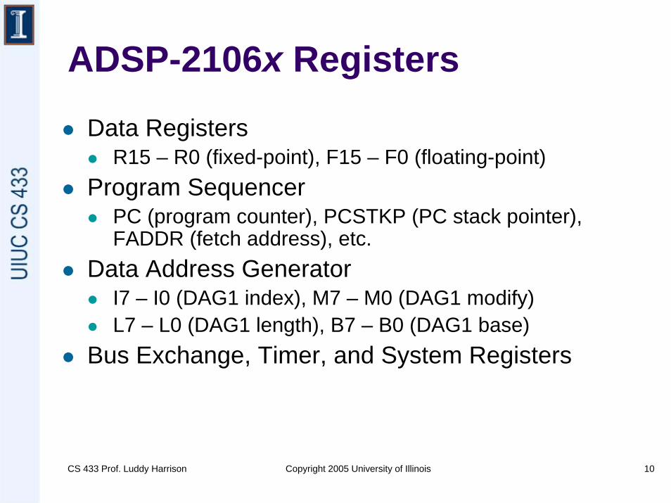
ADSP-2106x Registers
Data RegistersR15 – R0 (fixed-point), F15 – F0 (floating-point)
Program SequencerPC (program counter), PCSTKP (PC stack pointer), FADDR (fetch address), etc.
Data Address GeneratorI7 – I0 (DAG1 index), M7 – M0 (DAG1 modify)L7 – L0 (DAG1 length), B7 – B0 (DAG1 base)
Bus Exchange, Timer, and System Registers
CS 433 Prof. Luddy Harrison Copyright 2005 University of Illinois 11
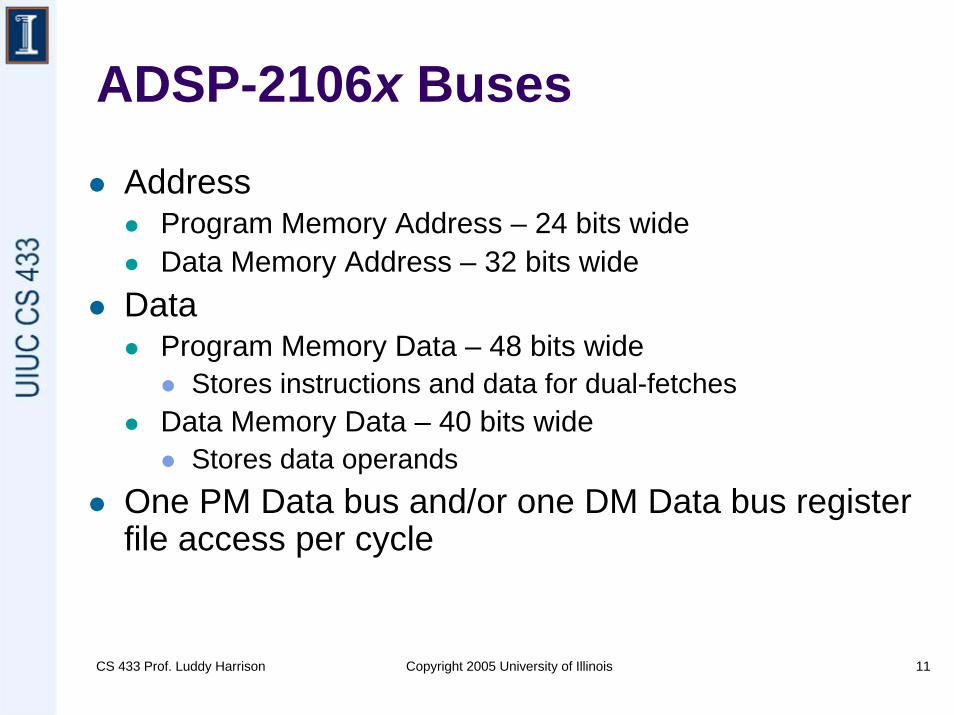
ADSP-2106x Buses
AddressProgram Memory Address – 24 bits wideData Memory Address – 32 bits wide
DataProgram Memory Data – 48 bits wide
Stores instructions and data for dual-fetchesData Memory Data – 40 bits wide
Stores data operandsOne PM Data bus and/or one DM Data bus register file access per cycle
CS 433 Prof. Luddy Harrison Copyright 2005 University of Illinois 12
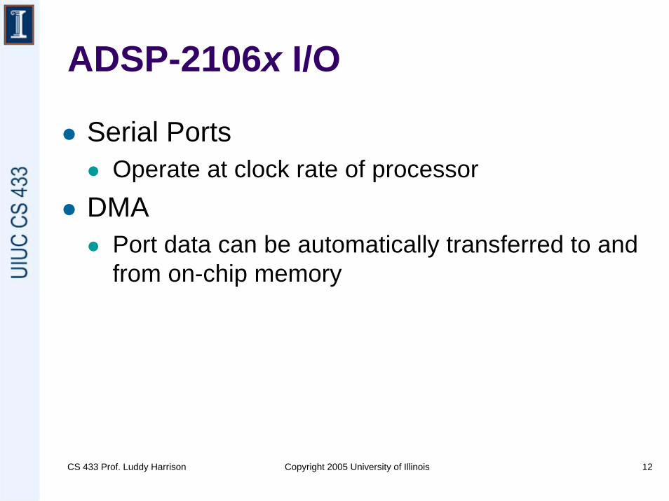
ADSP-2106x I/O
Serial PortsOperate at clock rate of processor
DMAPort data can be automatically transferred to and from on-chip memory
CS 433 Prof. Luddy Harrison Copyright 2005 University of Illinois 13
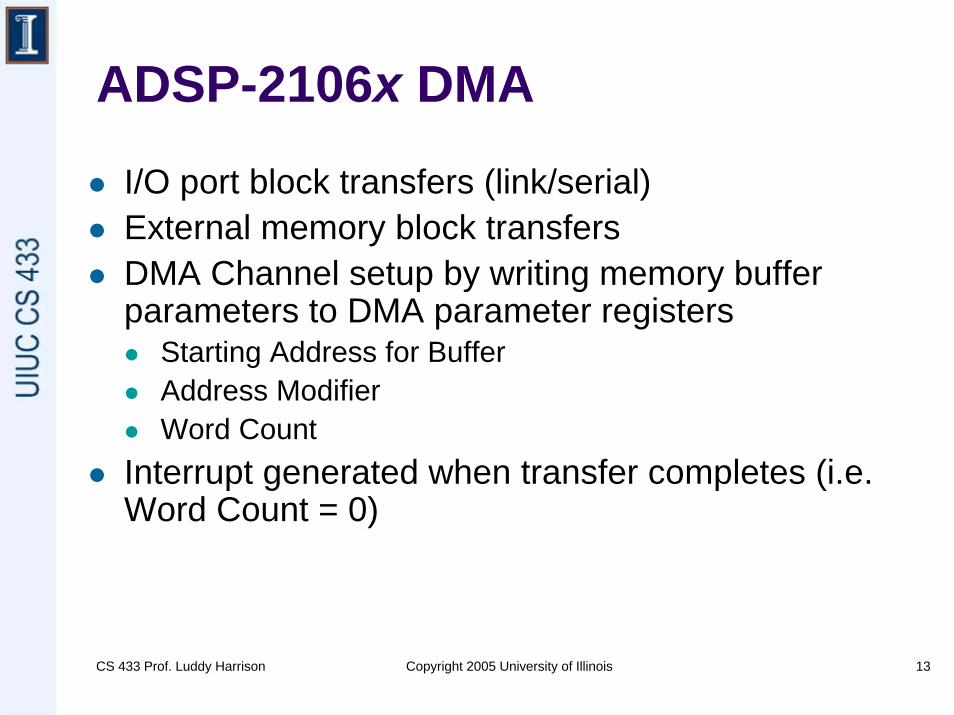
ADSP-2106x DMA
I/O port block transfers (link/serial)External memory block transfers DMA Channel setup by writing memory buffer parameters to DMA parameter registers
Starting Address for BufferAddress ModifierWord Count
Interrupt generated when transfer completes (i.e. Word Count = 0)
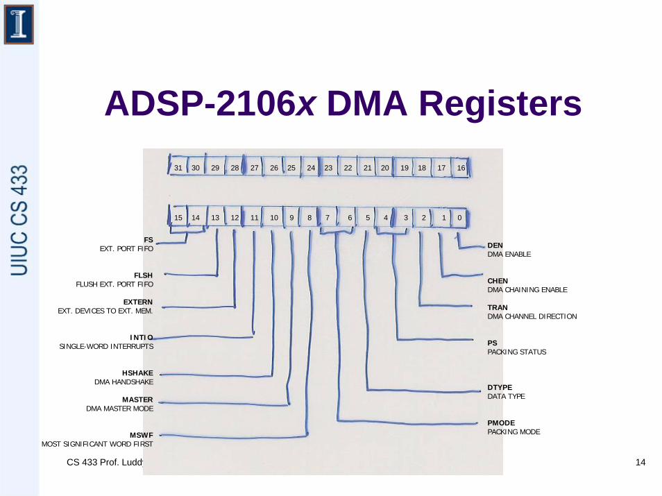
CS 433 Prof. Luddy Harrison Copyright 2005 University of Illinois 14
ADSP-2106x DMA Registers31 30 29 28 27 26 25 24 23 22 21 20 19 18 17 16
15 14 13 12 11 10 9 8 7 6 5 4 3 2 1 0
FSEXT. PORT FIFO
FLSHFLUSH EXT. PORT FIFO
EXTERNEXT. DEVICES TO EXT. MEM.
INTIOSINGLE-WORD INTERRUPTS
HSHAKEDMA HANDSHAKE
MASTERDMA MASTER MODE
MSWFMOST SIGNIFICANT WORD FIRST
DENDMA ENABLE
CHENDMA CHAINING ENABLE
TRANDMA CHANNEL DIRECTION
PSPACKING STATUS
DTYPEDATA TYPE
PMODEPACKING MODE
CS 433 Prof. Luddy Harrison Copyright 2005 University of Illinois 15
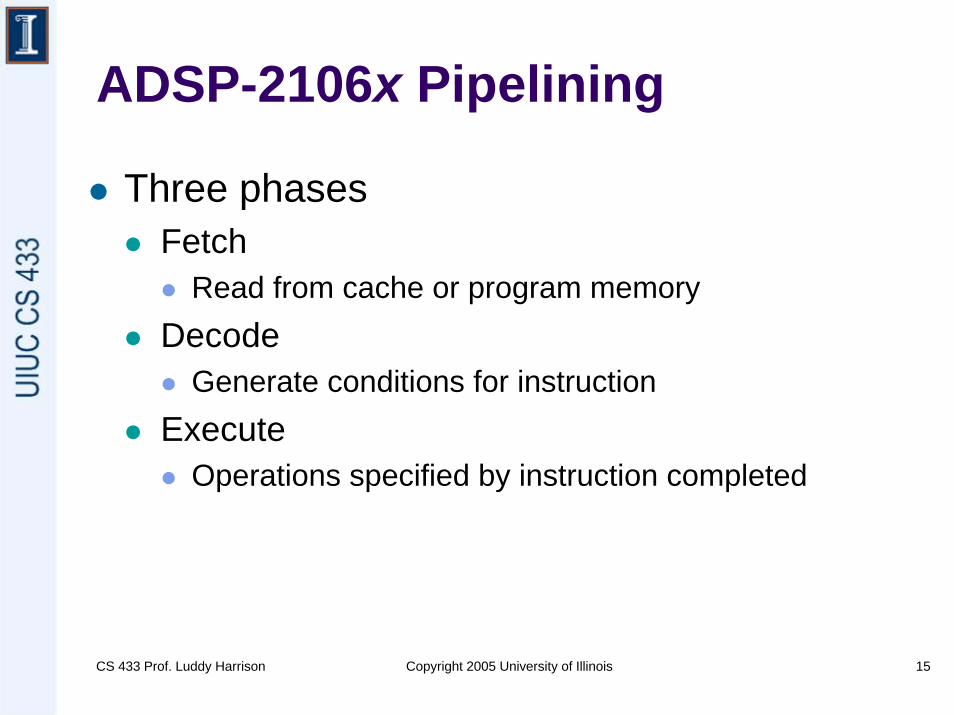
ADSP-2106x Pipelining
Three phasesFetch
Read from cache or program memoryDecode
Generate conditions for instructionExecute
Operations specified by instruction completed
CS 433 Prof. Luddy Harrison Copyright 2005 University of Illinois 16
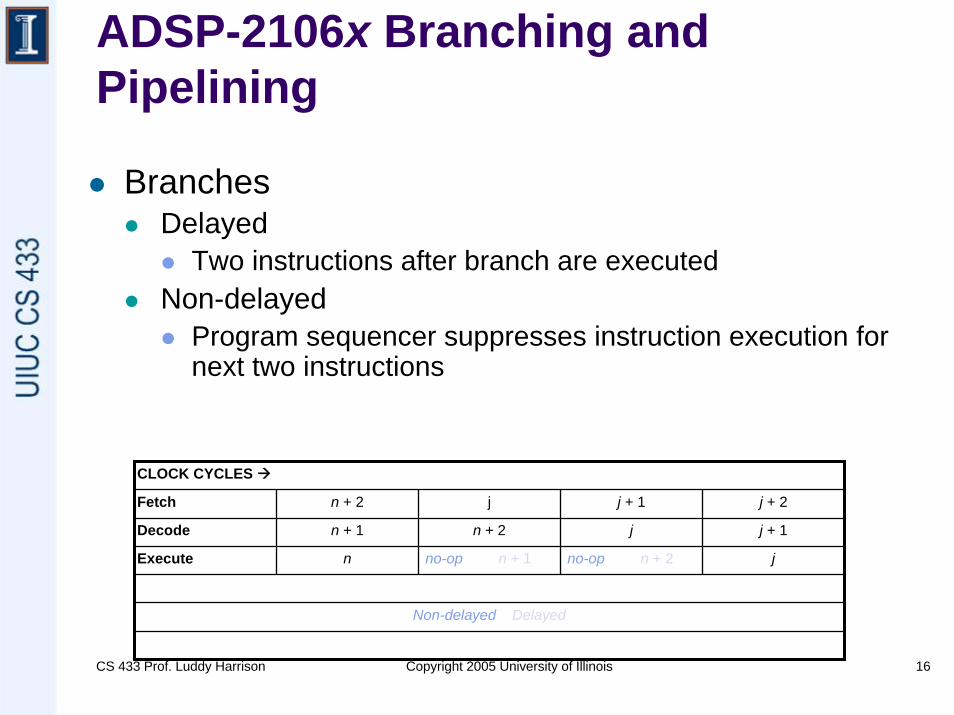
ADSP-2106x Branching and Pipelining
BranchesDelayed
Two instructions after branch are executedNon-delayed
Program sequencer suppresses instruction execution for next two instructions
CLOCK CYCLES
Fetch n + 2 j j + 1 j + 2
Decode n + 1 n + 2 j j + 1
Execute n no-op n + 1 no-op n + 2 j
Non-delayed Delayed
CS 433 Prof. Luddy Harrison Copyright 2005 University of Illinois 17
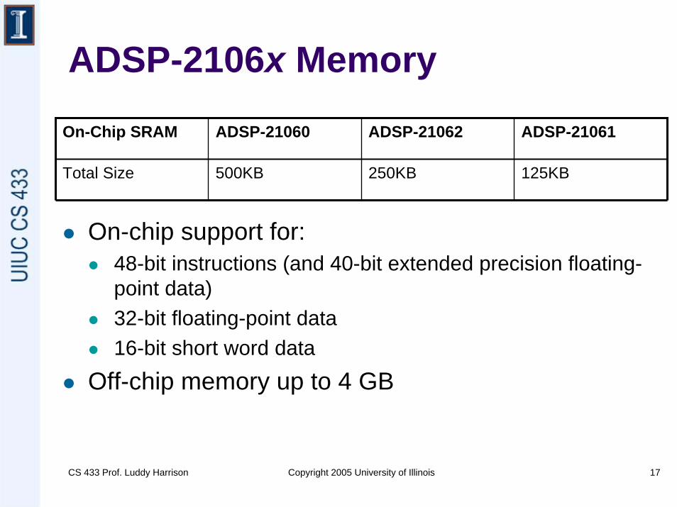
ADSP-2106x Memory
On-Chip SRAM ADSP-21060 ADSP-21062 ADSP-21061
Total Size 500KB 250KB 125KB
On-chip support for:48-bit instructions (and 40-bit extended precision floating-point data)32-bit floating-point data16-bit short word data
Off-chip memory up to 4 GB
CS 433 Prof. Luddy Harrison Copyright 2005 University of Illinois 18
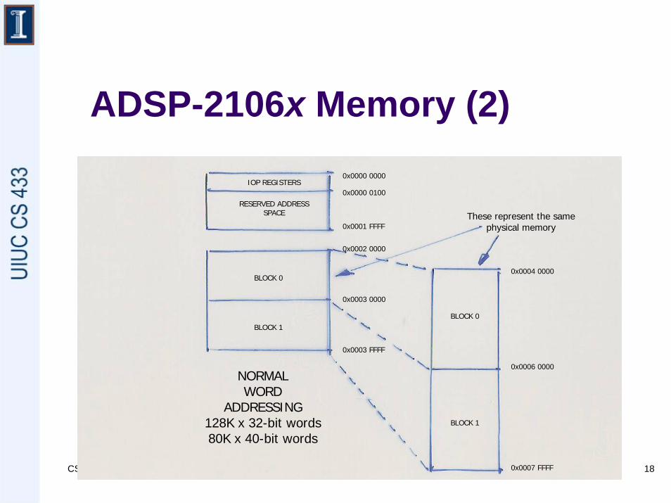
ADSP-2106x Memory (2)
IOP REGISTERS
RESERVED ADDRESSSPACE
BLOCK 0
BLOCK 1
These represent the samephysical memory
BLOCK 0
BLOCK 1
0x0004 0000
0x0006 0000
0x0007 FFFF
0x0000 0000
0x0000 0100
0x0001 FFFF
0x0002 0000
0x0003 0000
0x0003 FFFF
NORMALWORD
ADDRESSING128K x 32-bit words80K x 40-bit words
CS 433 Prof. Luddy Harrison Copyright 2005 University of Illinois 19
ADSP-2106x Memory (3)
Memory divided into blocksDual-ported (PM and DM bus share one port, I/O bus uses the other)
Allows independent access by processor core and I/O processorEach block can be accessed by both in every cycle
Typical DSP applications (digital filters, FFTs, etc.) access two operands at once, such as a filter coefficient and a data sample, so allowing single-cycle execution is a must
CS 433 Prof. Luddy Harrison Copyright 2005 University of Illinois 20
ADSP-2106x Shadow Write
Due to need for high-speed operations, memory writes to a two-deep FIFOOn write, data in FIFO from previous write is loaded to memory and new data enters FIFOReads of last two written locations are intercepted and re-routed to the FIFO
CS 433 Prof. Luddy Harrison Copyright 2005 University of Illinois 21
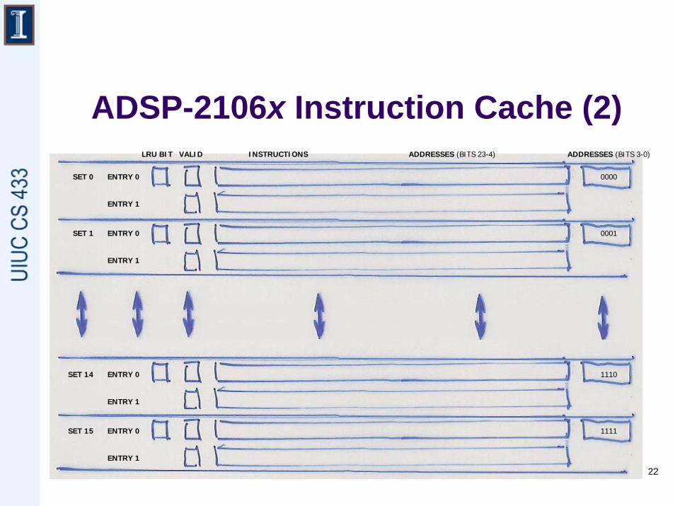
ADSP-2106x Instruction Cache
Sequencer checks instruction cache on every program memory data accessAllows PM bus to be used for data fetches instead of being tied up with an instruction fetchWhen fetch conflict first occurs, instruction is cached to prevent the same delay from happening again
CS 433 Prof. Luddy Harrison Copyright 2005 University of Illinois 22
ADSP-2106x Instruction Cache (2)
SET 0 ENTRY 0
ENTRY 1
LRU BIT VALID INSTRUCTIONS ADDRESSES (BITS 23-4) ADDRESSES (BITS 3-0)
0000
0001
1110
1111
SET 1 ENTRY 0
ENTRY 1
SET 14 ENTRY 0
ENTRY 1
SET 15 ENTRY 0
ENTRY 1
CS 433 Prof. Luddy Harrison Copyright 2005 University of Illinois 23
ADSP-2106x ISA Overview
24 operations, although some have more than one syntactical formInstruction Types
Compute and MoveCompute operation in parallel with data moves or index register modify
Program Flow ControlBranch, Call, Return, Loop
Immediate Data MoveOperand or addressing immediate fields
MiscellaneousBit Modify and Test, No-op, etc.
CS 433 Prof. Luddy Harrison Copyright 2005 University of Illinois 24
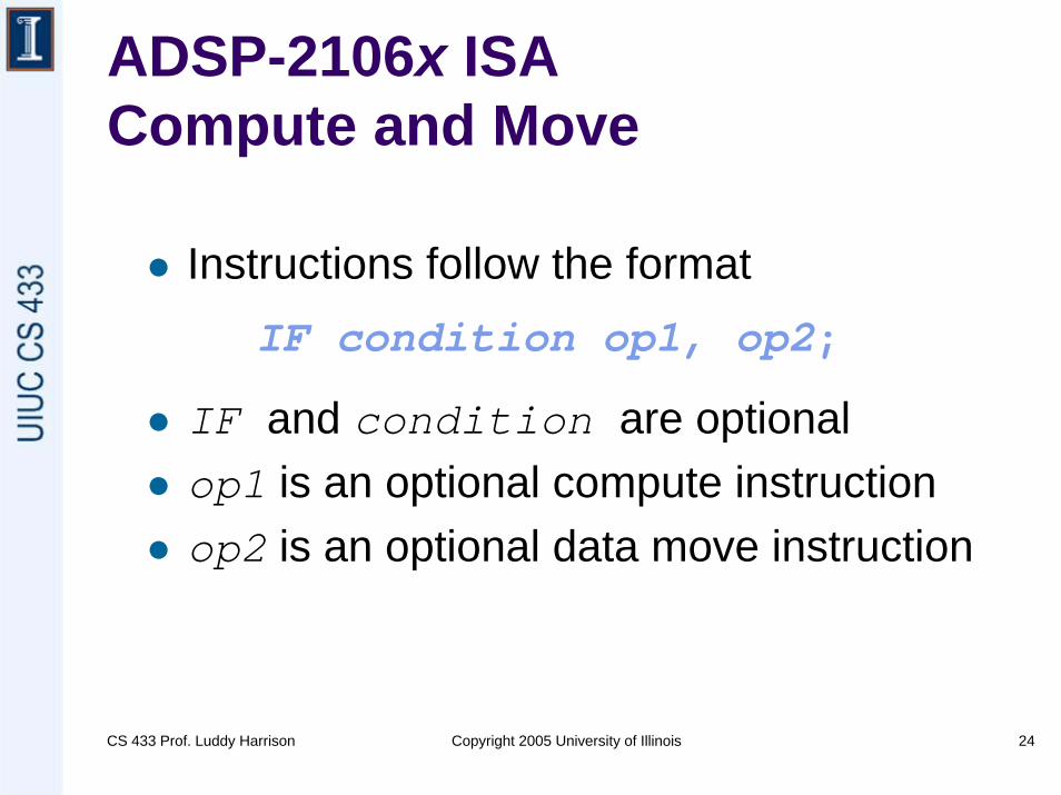
ADSP-2106x ISACompute and Move
Instructions follow the formatIF condition op1, op2;
IF and condition are optionalop1 is an optional compute instructionop2 is an optional data move instruction
CS 433 Prof. Luddy Harrison Copyright 2005 University of Illinois 25
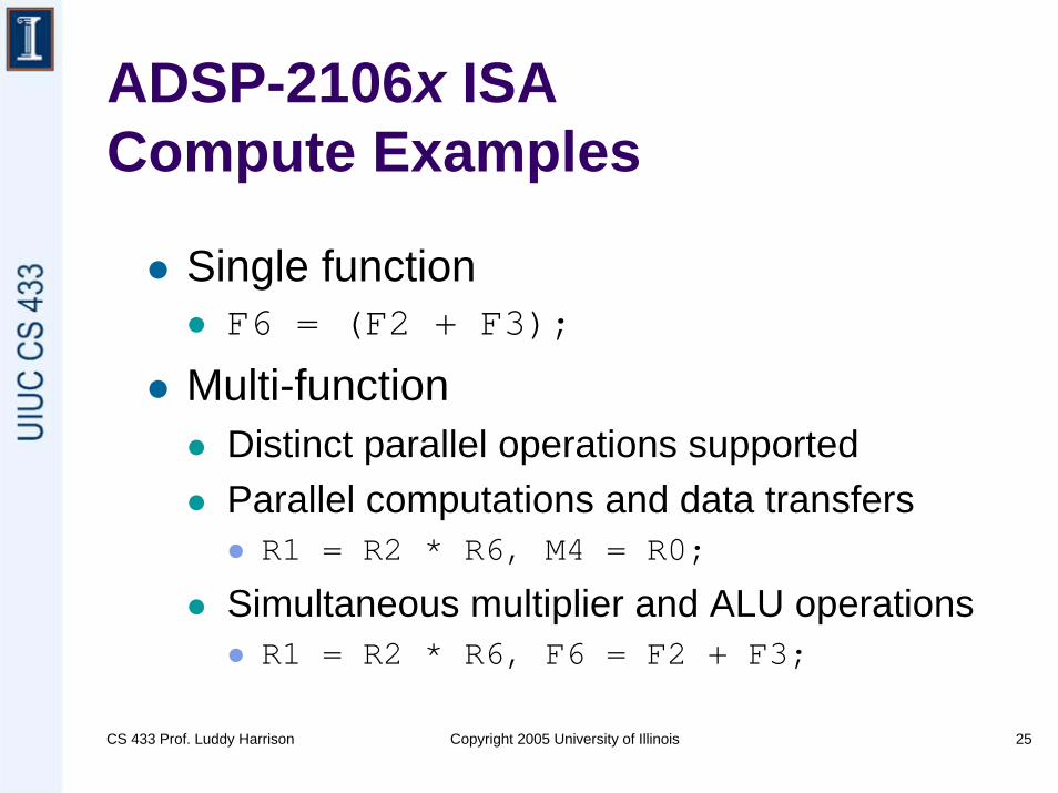
ADSP-2106x ISACompute Examples
Single functionF6 = (F2 + F3);
Multi-functionDistinct parallel operations supportedParallel computations and data transfersR1 = R2 * R6, M4 = R0;
Simultaneous multiplier and ALU operationsR1 = R2 * R6, F6 = F2 + F3;
CS 433 Prof. Luddy Harrison Copyright 2005 University of Illinois 26
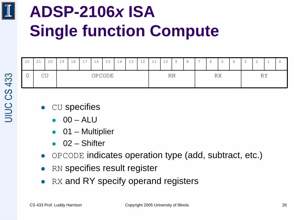
ADSP-2106x ISASingle function Compute
22 21 20 19 18 17 16 15 14 13 12 11 10 9 8 7 6 5 4 3 2 1 0
0 CU OPCODE RN RX RY
CU specifies00 – ALU01 – Multiplier02 – Shifter
OPCODE indicates operation type (add, subtract, etc.)RN specifies result registerRX and RY specify operand registers
CS 433 Prof. Luddy Harrison Copyright 2005 University of Illinois 27
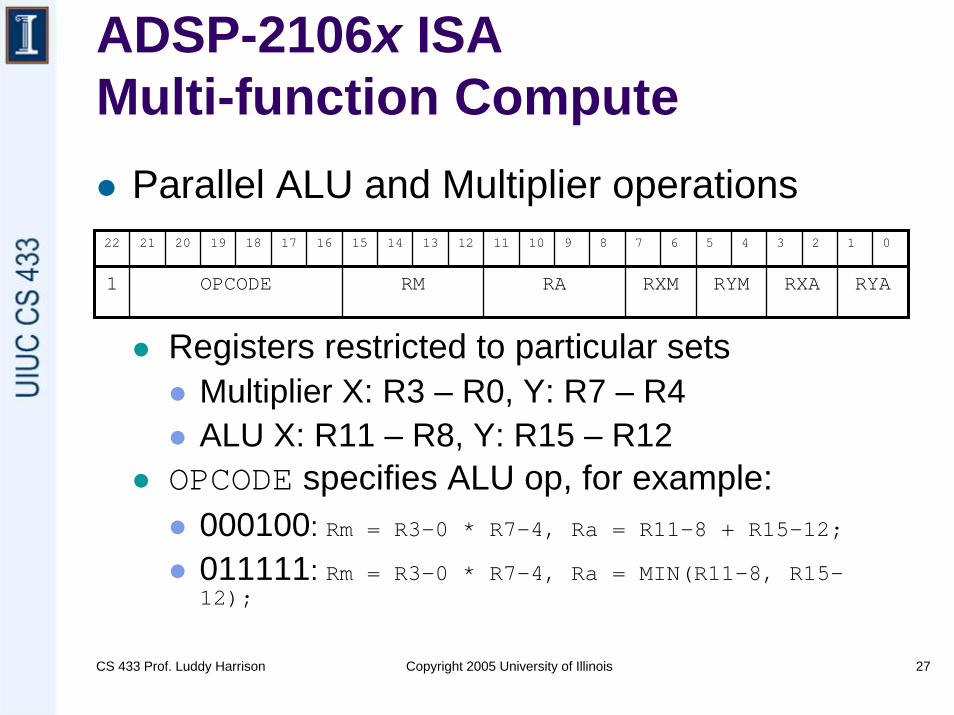
ADSP-2106x ISAMulti-function Compute
22 21 20 19 18 17 16 15 14 13 12 11 10 9 8 7 6 5 4 3 2 1 0
1 OPCODE RM RA RXM RYM RXA RYA
Parallel ALU and Multiplier operations
Registers restricted to particular setsMultiplier X: R3 – R0, Y: R7 – R4ALU X: R11 – R8, Y: R15 – R12
OPCODE specifies ALU op, for example:000100: Rm = R3-0 * R7-4, Ra = R11-8 + R15-12;
011111: Rm = R3-0 * R7-4, Ra = MIN(R11-8, R15-12);
CS 433 Prof. Luddy Harrison Copyright 2005 University of Illinois 28
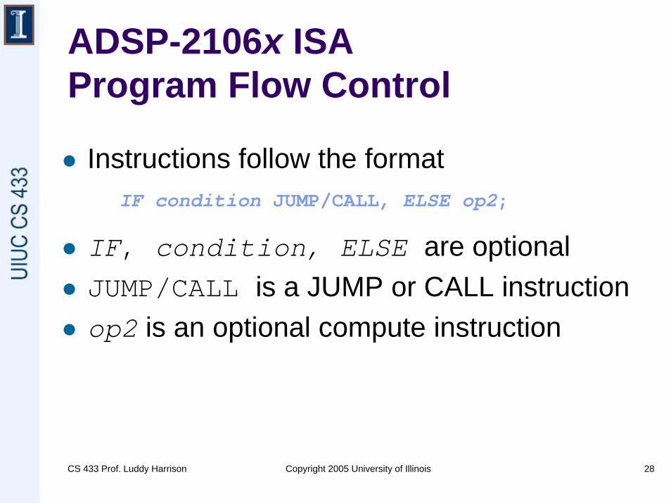
ADSP-2106x ISAProgram Flow Control
Instructions follow the formatIF condition JUMP/CALL, ELSE op2;
IF, condition, ELSE are optionalJUMP/CALL is a JUMP or CALL instruction op2 is an optional compute instruction
CS 433 Prof. Luddy Harrison Copyright 2005 University of Illinois 29
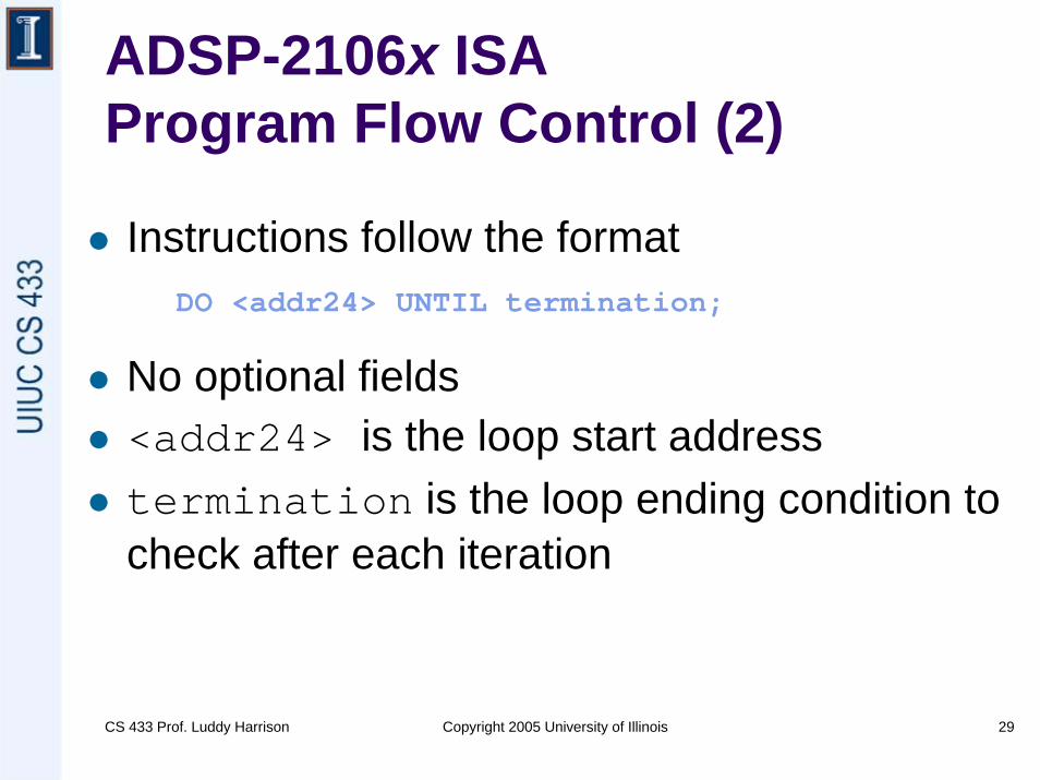
ADSP-2106x ISAProgram Flow Control (2)
Instructions follow the formatDO <addr24> UNTIL termination;
No optional fields<addr24> is the loop start addresstermination is the loop ending condition to check after each iteration
CS 433 Prof. Luddy Harrison Copyright 2005 University of Illinois 30
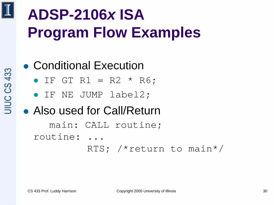
ADSP-2106x ISAProgram Flow Examples
Conditional ExecutionIF GT R1 = R2 * R6;IF NE JUMP label2;
Also used for Call/Returnmain: CALL routine;
routine: ...RTS; /*return to main*/
CS 433 Prof. Luddy Harrison Copyright 2005 University of Illinois 31
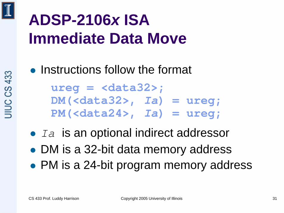
ADSP-2106x ISAImmediate Data Move
Instructions follow the formatureg = <data32>;DM(<data32>, Ia) = ureg;PM(<data24>, Ia) = ureg;
Ia is an optional indirect addressorDM is a 32-bit data memory addressPM is a 24-bit program memory address
CS 433 Prof. Luddy Harrison Copyright 2005 University of Illinois 32
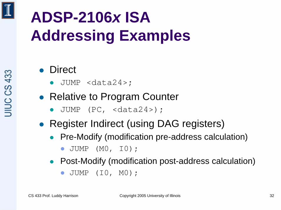
ADSP-2106x ISAAddressing Examples
DirectJUMP <data24>;
Relative to Program CounterJUMP (PC, <data24>);
Register Indirect (using DAG registers)Pre-Modify (modification pre-address calculation)JUMP (M0, I0);
Post-Modify (modification post-address calculation)JUMP (I0, M0);
CS 433 Prof. Luddy Harrison Copyright 2005 University of Illinois 33
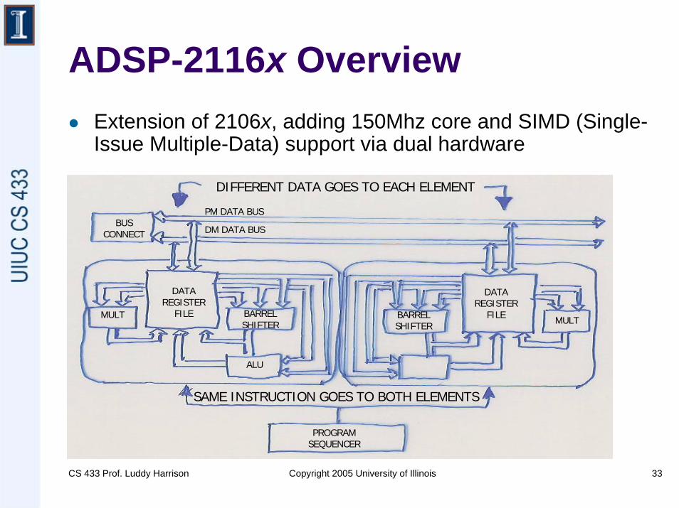
ADSP-2116x OverviewExtension of 2106x, adding 150Mhz core and SIMD (Single-Issue Multiple-Data) support via dual hardware
DIFFERENT DATA GOES TO EACH ELEMENT
PM DATA BUS
DM DATA BUSBUS
CONNECT
MULT
DATAREGISTER
FILE BARRELSHIFTER
ALU
MULT
DATAREGISTER
FILEBARRELSHIFTER
PROGRAMSEQUENCER
SAME INSTRUCTION GOES TO BOTH ELEMENTS
CS 433 Prof. Luddy Harrison Copyright 2005 University of Illinois 34
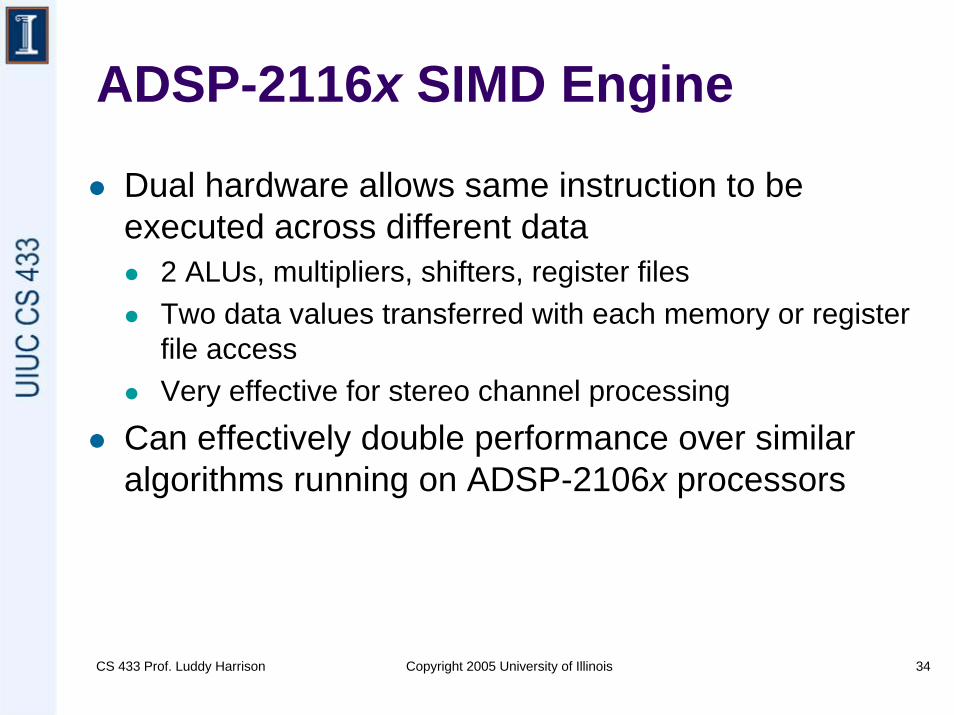
ADSP-2116x SIMD Engine
Dual hardware allows same instruction to be executed across different data
2 ALUs, multipliers, shifters, register filesTwo data values transferred with each memory or register file accessVery effective for stereo channel processing
Can effectively double performance over similar algorithms running on ADSP-2106x processors
CS 433 Prof. Luddy Harrison Copyright 2005 University of Illinois 35
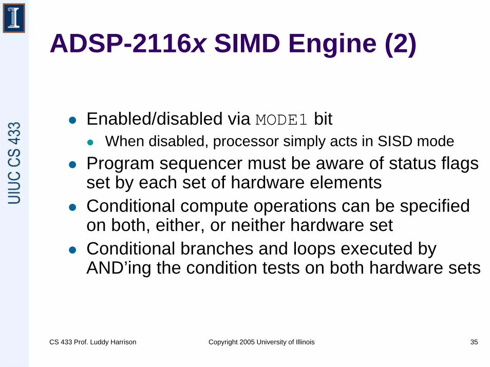
ADSP-2116x SIMD Engine (2)
Enabled/disabled via MODE1 bitWhen disabled, processor simply acts in SISD mode
Program sequencer must be aware of status flags set by each set of hardware elementsConditional compute operations can be specified on both, either, or neither hardware setConditional branches and loops executed by AND’ing the condition tests on both hardware sets
CS 433 Prof. Luddy Harrison Copyright 2005 University of Illinois 36
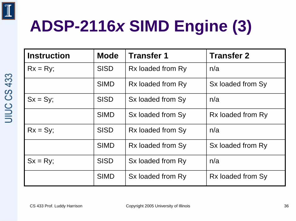
ADSP-2116x SIMD Engine (3)Instruction Mode Transfer 1 Transfer 2Rx = Ry; SISD Rx loaded from Ry n/a
SIMD Rx loaded from Ry Sx loaded from Sy
Sx = Sy; SISD Sx loaded from Sy n/a
SIMD Sx loaded from Ry Rx loaded from Sy
SIMD Sx loaded from Sy Rx loaded from Ry
Rx = Sy; SISD Rx loaded from Sy n/a
SIMD Rx loaded from Sy Sx loaded from Ry
Sx = Ry; SISD Sx loaded from Ry n/a
CS 433 Prof. Luddy Harrison Copyright 2005 University of Illinois 37
ADSP-2126x Overview
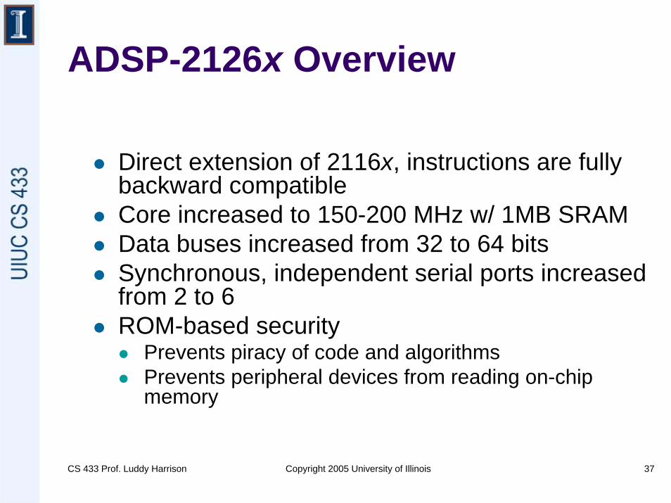
Direct extension of 2116x, instructions are fully backward compatibleCore increased to 150-200 MHz w/ 1MB SRAMData buses increased from 32 to 64 bitsSynchronous, independent serial ports increased from 2 to 6ROM-based security
Prevents piracy of code and algorithmsPrevents peripheral devices from reading on-chip memory
CS 433 Prof. Luddy Harrison Copyright 2005 University of Illinois 38
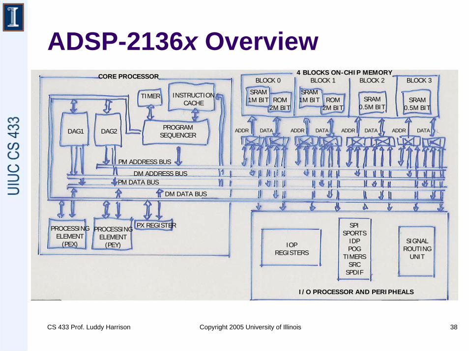
ADSP-2136x OverviewCORE PROCESSOR
DAG1 DAG2 PROGRAMSEQUENCER
TIMER INSTRUCTIONCACHE
PROCESSINGELEMENT
(PEX)
PROCESSINGELEMENT
(PEY)
PX REGISTER
PM ADDRESS BUS
DM ADDRESS BUSPM DATA BUS
DM DATA BUS
4 BLOCKS ON-CHIP MEMORYBLOCK 0 BLOCK 1 BLOCK 2 BLOCK 3
SRAM1M BIT
SRAM1M BIT SRAM
0.5M BITSRAM
0.5M BITROM
2M BITROM
2M BIT
IOP REGISTERS
I/O PROCESSOR AND PERIPHEALS
SIGNALROUTING
UNIT
SPISPORTS
IDPPOG
TIMERSSRC
SPDIF
ADDR DATA ADDR DATA ADDR DATA ADDR DATA
CS 433 Prof. Luddy Harrison Copyright 2005 University of Illinois 39
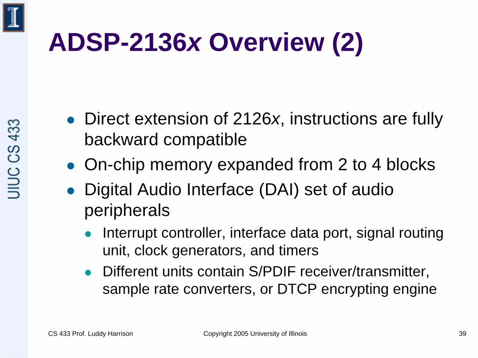
ADSP-2136x Overview (2)
Direct extension of 2126x, instructions are fully backward compatible On-chip memory expanded from 2 to 4 blocksDigital Audio Interface (DAI) set of audio peripherals
Interrupt controller, interface data port, signal routing unit, clock generators, and timersDifferent units contain S/PDIF receiver/transmitter, sample rate converters, or DTCP encrypting engine
CS 433 Prof. Luddy Harrison Copyright 2005 University of Illinois 40
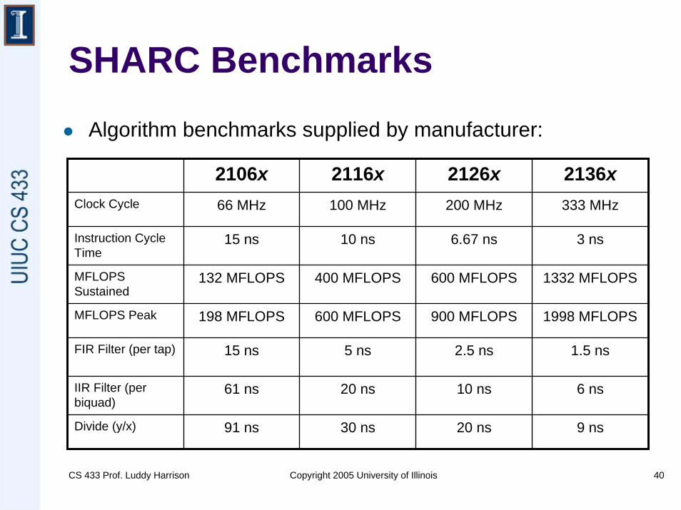
SHARC BenchmarksAlgorithm benchmarks supplied by manufacturer:
2106x 2116x 2126x 2136xClock Cycle 66 MHz 100 MHz 200 MHz 333 MHz
Instruction Cycle Time
15 ns 10 ns 6.67 ns 3 ns
MFLOPS Sustained
132 MFLOPS 400 MFLOPS 600 MFLOPS 1332 MFLOPS
MFLOPS Peak 198 MFLOPS 600 MFLOPS 900 MFLOPS 1998 MFLOPS
FIR Filter (per tap) 15 ns 5 ns 2.5 ns 1.5 ns
IIR Filter (per biquad)
61 ns 20 ns 10 ns 6 ns
Divide (y/x) 91 ns 30 ns 20 ns 9 ns
CS 433 Prof. Luddy Harrison Copyright 2005 University of Illinois 41
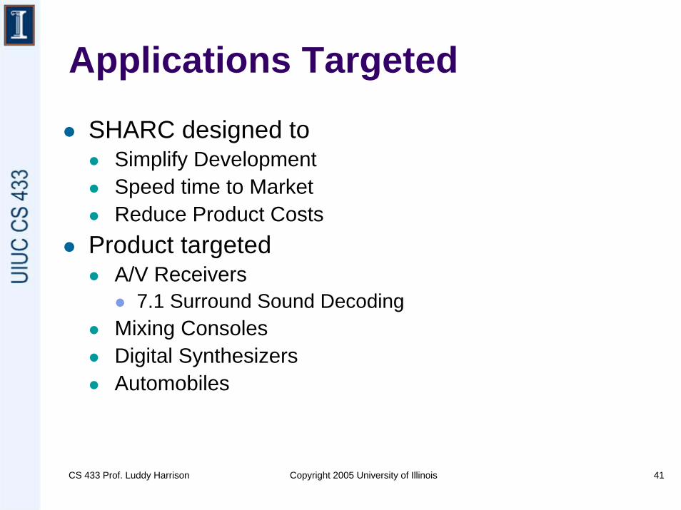
Applications Targeted
SHARC designed toSimplify DevelopmentSpeed time to MarketReduce Product Costs
Product targetedA/V Receivers
7.1 Surround Sound DecodingMixing ConsolesDigital SynthesizersAutomobiles
CS 433 Prof. Luddy Harrison Copyright 2005 University of Illinois 42
Systems Employing the SHARC
SRS Circle Surround IIMelody (w/ Auto Room Tuner)Metric Halo's Portable Pro Audio HubAlacron FT-P5
CS 433 Prof. Luddy Harrison Copyright 2005 University of Illinois 43
SHARC in SRS Circle Surround II
Full multi-channel surround sound from simple right/left stereo soundEncoding can be transmitted over standard stereo medium (broadcast television, radio, etc.) and maintains full backward compatibility
CS 433 Prof. Luddy Harrison Copyright 2005 University of Illinois 44
SHARC in SRS Circle Surround II (2)Output from each source is combined in constant phase filter banks and encoded in quadrature to prevent signal cancellation“Positional bias generator” analyzes ratios between left and right surround signals which multipliers then apply to the opposing left or right outputDecoder uses this level imbalance to direct the surround information to the correct output
CS 433 Prof. Luddy Harrison Copyright 2005 University of Illinois 45
SHARC Melody
“Optimized Surround Sound for the Mass Market”Core of high-fidelity audio decoders in Denon, Bose, and Kenwood productsAuto Room Tuner (ART) integrated software simplifies setup of complex audio systems
CS 433 Prof. Luddy Harrison Copyright 2005 University of Illinois 46
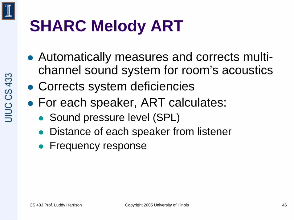
SHARC Melody ART
Automatically measures and corrects multi-channel sound system for room’s acousticsCorrects system deficienciesFor each speaker, ART calculates:
Sound pressure level (SPL) Distance of each speaker from listenerFrequency response
CS 433 Prof. Luddy Harrison Copyright 2005 University of Illinois 47
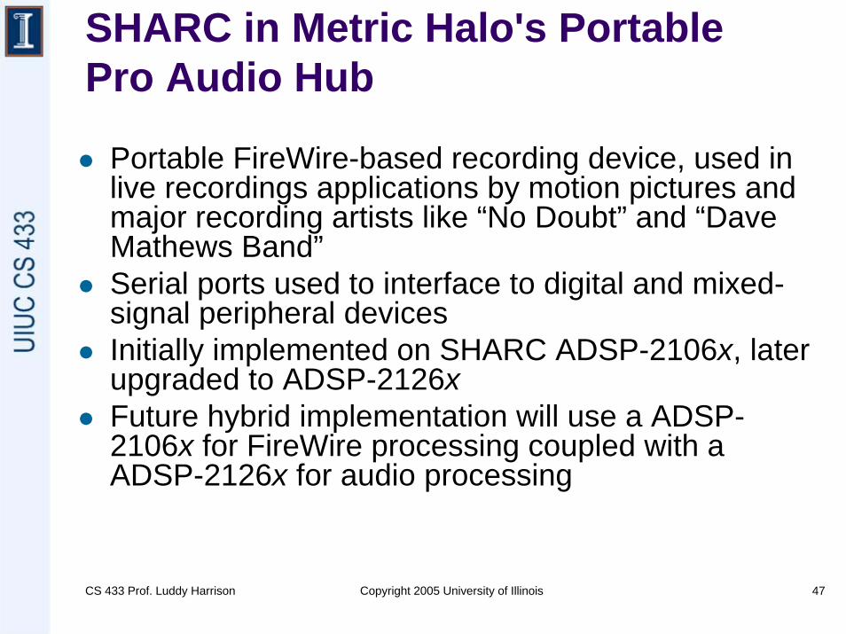
SHARC in Metric Halo's Portable Pro Audio Hub
Portable FireWire-based recording device, used in live recordings applications by motion pictures and major recording artists like “No Doubt” and “Dave Mathews Band”Serial ports used to interface to digital and mixed-signal peripheral devices Initially implemented on SHARC ADSP-2106x, later upgraded to ADSP-2126xFuture hybrid implementation will use a ADSP-2106x for FireWire processing coupled with a ADSP-2126x for audio processing
CS 433 Prof. Luddy Harrison Copyright 2005 University of Illinois 48
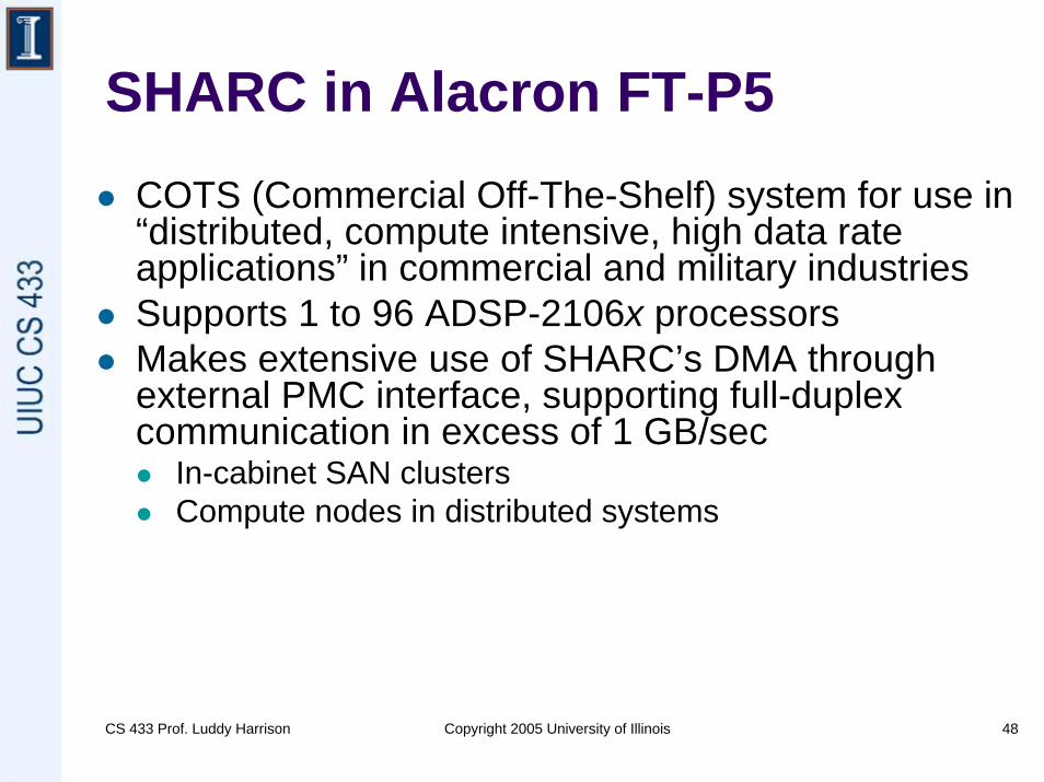
SHARC in Alacron FT-P5COTS (Commercial Off-The-Shelf) system for use in “distributed, compute intensive, high data rate applications” in commercial and military industriesSupports 1 to 96 ADSP-2106x processorsMakes extensive use of SHARC’s DMA through external PMC interface, supporting full-duplex communication in excess of 1 GB/sec
In-cabinet SAN clustersCompute nodes in distributed systems
CS 433 Prof. Luddy Harrison Copyright 2005 University of Illinois 49
SHARC vs. RISC Processors
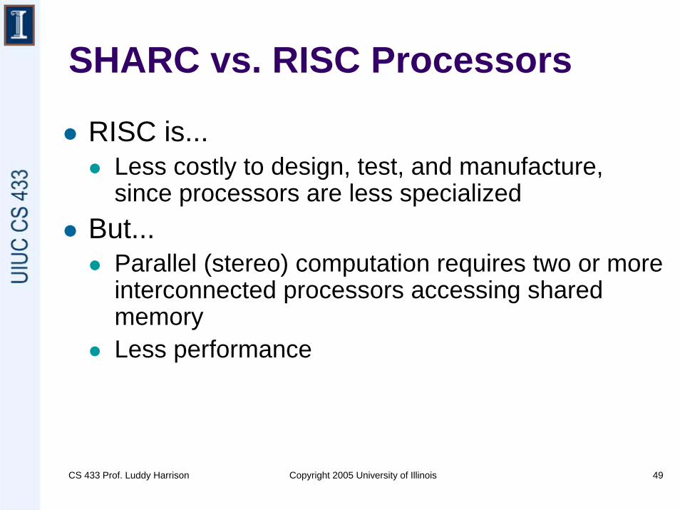
RISC is...Less costly to design, test, and manufacture, since processors are less specialized
But...Parallel (stereo) computation requires two or more interconnected processors accessing shared memoryLess performance
CS 433 Prof. Luddy Harrison Copyright 2005 University of Illinois 50
Conclusion
SHARC offers great deal of computational power, with on-chip SRAM and SIMD architectureVariety of applications (especially audio processing) exploit it
CS 433 Prof. Luddy Harrison Copyright 2005 University of Illinois 51
Citations
Processor details taken from product manuals and descriptions at http://www.analog.com


![Exergy Analysis of a Pilot Parabolic Solar Dish-Stirling ...€¦ · A new solar dish configuration was developed by Ahmed [10], in which, compared to a usual dish, the focal point](https://img.pdfslide.us/doc/110x75/5ea9b0fb49882e5d4b7c8956/exergy-analysis-of-a-pilot-parabolic-solar-dish-stirling-a-new-solar-dish-coniguration.jpg)