Embed Size (px)
Citation preview

A digital method to determine the transmissibility of a MEMS device
by
Yixuan Wu
A thesis submitted to the Graduate Faculty of
Auburn University
in partial fulfillment of the
requirements for the Degree of
Master of Science
Auburn, Alabama
May 5, 2014
Key words: transmissibility, microcontroller, Modified FFT
Copyright 2014 by Yixuan Wu
Approved by
Robert Dean, Chair, Associate Professor of Electrical and Computer Engineering
Thomas Baginski, Professor of Electrical and Computer Engineering
Thaddeus Roppel, Associate Professor of Electrical and Computer Engineering

ii
Abstract
A microcontroller based technique for measuring the transmissibility of a
MEMS device is very useful and meaningful. The resulting data can provide feedback to
improve the design, modeling and fabrication process. A new method for measuring the
transmissibility has been investigated using a microcontroller where the results are
displayed on a personal computer real time. The microcontroller used in the research is
the Stm32f407. The purpose of the application is proposed and the practicability is
investigated as well. A cantilevered structure and three materials are chosen to verify the
technique. The cost for the implementation is estimated and found to be low. The
resulting technique can be used in research to process the transmissibility data real time
and analyze the data for future applications.

iii
Acknowledgments
I would like to thank my advisor, Dr. Robert Dean, without whom none of this
work could have been done. His wise instruction and patient support provided me with
constant help to deal with every academic problem. I would also like to thank to Dr. Thomas
Baginski and Dr. Thaddeus Roppel for their guidance of my graduate studies. I would also
like to thank Chong Li, Haoyue Yang and Luke L. Jenkins for their generous help throughout
this project. Without their help, the design would have been difficult to finish. I am also
appreciative of my parents for their consistent support.

iv
Table of Contents
Abstract ................................................................................................................................................ ii
Acknowledgments .............................................................................................................................. iii
List of Figures ....................................................................................................................................... vi
List of Abbreviations ............................................................................................................................. ix
List of Tables.......................................................................................................................................... x
Chapter 1 Introduction ...................................................................................................................... 1
Chapter 2 Literature Review .............................................................................................................. 3
Section 1 MEMS ................................................................................................................... 3
Section2 Transmissibility ...................................................................................................... 4
Section3 Ways to analyze the transmissibility ..................................................................... 12
Section4 Sampling and FFT..................................................................................................... 16
Chapter 3 Tools used in the research ............................................................................................... 27
Section1 Microcontroller........................................................................................................ 27
Section2 VCP.......................................................................................................................... 34
Section3 GUI ...................................................................................................................... 34
Chapter4 Design principle ................................................................................................................ 36
Section1 The configuration of ADC ..................................................................................... 38
Section2 Modified FFT algorithm .......................................................................................... 44
v
Section3 VCP design ........................................................................................................... 46
Section4 Design of GUI ....................................................................................................... 47
Chapter5 Test .................................................................................................................................. 53
Section1 Test by function generator ..................................................................................... 53
Section2 Assembling ............................................................................................................ 58
Section3 Compared with results from Hp 35665 analyzer ..................................................... 63
Chapter6 Conclusion and future work ............................................................................................... 72
References ...................................................................................................................................... 74
Appendix ....................................................................................................................................... 77

vi
List of Figures
Figure1 .............................................................................................................................................. 4
Figure2 .............................................................................................................................................. 8
Figure3 ............................................................................................................................................ 12
Figure4 ............................................................................................................................................ 14
Figure5 ............................................................................................................................................ 17
Figure6 ............................................................................................................................................ 18
Figure7 ............................................................................................................................................ 18
Figure8 ............................................................................................................................................ 19
Figure9 ............................................................................................................................................ 19
Figure10 .......................................................................................................................................... 19
Figure11 .......................................................................................................................................... 20
Figure12 .......................................................................................................................................... 23
Figure13 .......................................................................................................................................... 23
Figure14 .......................................................................................................................................... 24
Figure15 .......................................................................................................................................... 25
Figure16 .......................................................................................................................................... 26
Figure17 .......................................................................................................................................... 26
Figure18 .......................................................................................................................................... 31
Figure19 .......................................................................................................................................... 31
Figure20 .......................................................................................................................................... 36
vii
Figure21 .......................................................................................................................................... 38
Figure22 .......................................................................................................................................... 42
Figure23 .......................................................................................................................................... 43
Figure24 .......................................................................................................................................... 48
Figure25 .......................................................................................................................................... 50
Figure26 .......................................................................................................................................... 51
Figure27 .......................................................................................................................................... 53
Figure28 .......................................................................................................................................... 55
Figure29 ............................................................................................................................................ 56
Figure30 ............................................................................................................................................ 57
Figure31 ............................................................................................................................................ 58
Figure32 ............................................................................................................................................ 60
Figure33 ............................................................................................................................................ 61
Figure34 ............................................................................................................................................ 62
Figure35 ............................................................................................................................................ 62
Figure36 ............................................................................................................................................ 63
Figure37 ............................................................................................................................................ 64
Figure38 ............................................................................................................................................ 65
Figure39 ............................................................................................................................................ 65
Figure40 ............................................................................................................................................ 66
Figure41 ............................................................................................................................................ 66
Figure42 ............................................................................................................................................ 67

viii
Figure43 ............................................................................................................................................ 68
Figure44 ............................................................................................................................................ 69
Figure45 ............................................................................................................................................ 69
Figure46 ............................................................................................................................................ 70
Figure47 ............................................................................................................................................ 71

ix
List of Abbreviations
APB Advanced Peripheral Bus
ADC Analog-to-digital Converter
DMA Direct Memory Access
DAC Digital-to-Analog Converter
DFT Discrete Fourier Transform
GUI Graphical User Interface
FFT FAST Fourier Transform
FSM Finite state Machine
IDFT Inverse Discrete Fourier Transform
MCU Microcontroller Unit
PIC Peripheral Interface Controller
SDOF Single Degree of Freedom
USB Universal Serial Bus
VCP Virtual COM port

x
List of tables
Table1 ................................................................................................................................................. 1
Table2 ................................................................................................................................................. 1

1
Chapter 1 Introduction
The relation between force on physical systems and the motion caused by the
force is a subject that has been studied by humans since ancient times. The analysis and
prediction for the dynamic character of physical systems is important for modern
engineering. One omnipresent kind of dynamic behavior is vibration, where the system
oscillates about a certain equilibrium position. The research for the thesis is to develop a
microcontroller based system to measure the transmissibility of a vibrating MEMS structure.
The analysis of transmissibility is an effective method to analyze the MEMS
device’s characteristics and vibration features. The transmissibility can display two important
characteristics for MEMS device, one is resonant frequency and the other is mechanical
quality factor. A dynamic signal analyzer is often used to analyze the transmissibility of the
MEMS device. It is relatively a high cost and complex piece of laboratory test equipment.
Furthermore, the transmissibility is difficult to extract from the analyzer in real time. Finding
a convenient and simple way to measure the transmissibility of a MEMS device in real time is
considered in this research. The Stm32f407 microcontroller is based on the
high-performance ARM Cortex M4 32-bit RISC core, which has a sufficiently strong
calculation ability. By using a Stm32f407, the output and input data of the MEMS device
under test can be extracted and processed. For the MEMS device, the ratio of the
magnitudes of the output to the input of the vibration is the transmissibility of the system. A
modified FFT algorithm is used to transform the system from time domain to frequency
domain. Visual studio is used to display the results, with a refresh period of 4 seconds. By

2
averaging the data, the noise in the data can be decreased and the figure will be updated
every 20s. A function generator is used to preliminary verify the results, and then a vibration
system and a laser system are used to test the accuracy of the results for the device under
test. From the results, the resonant frequency of a MEMS device can be determined from
the transmissibility plot for the MEMS device and this information can be observed in real
time successfully. This results if this research can reduce the cost of the equipment and can
meet the requirement to display the data in real time.
Furthermore, the data to display the transmissibility can be written out to a
personal computer real time, and it is easy to take the data and analyze it, thus it will be
helpful to the MEMS researcher.

3
Chapter 2 Literature review
Section 1 MEMS
Micro-electro-mechanical Systems (MEMS) can be defined as a technology of
miniaturized mechanical and electro-mechanical elements which are made by the process of
microfabrication. MEMS technology evolved from the integrated circuit industry.
Microfabrication is the engine for MEMS. From the 1990s, the development of MEMS came
to a worldwide rapid and dynamic growth period. Two applications are notable; one is the
integrated inertial sensor that is made by Analog Devices for the deployment of automotive
air-bags, and the other is the Digital Light Processing chip that is made by Texas Instruments
for projection displays. MEMS have the advantages of high sensitivity and low noise, and it
also reduces the costs of each sensor by removing manual assembly steps and by using batch
fabrication to manufacture them. Nowadays, one can find that different micromachined
acceleration sensors are the basis of sensing principles and fabrication technologies.
Furthermore, they have better features and better reliability. In all, MEMS has three generic
and distinct merits, microelectronics integration, miniaturization, and mass fabrication with
precision.

4
Section 2 Transmissibility
Figure 1 shows two types of mechanical oscillator; they can be seen as
simple mechannical systems.
(a) (b)
Figure 1 Mechanical System
Mechanical resonance
Mechanical resonance is a kind of response of the mechanical system where it
can obtain the highest amplitude of motion at that frequency when subjected to a force with
components at that frequency. The mechanical system can sometimes experience violent

5
swaying motions at the resonant frequency, and furthermore, this has the possibility to
cause catastrophic failure for structures such as bridges, buildings and airplanes if they are
designed improperly. Commonly, a dynamic signal analyzer is used to test the mechanical
resonance.
To find the mechanical resonance is to find the resonance of a mechanical oscillator.
Any mechanical body, if it is free to vibrate, has its natural periods of oscillation. For an
example, a thin steel rod, when it is struck, will oscillate if it is held at one end. The
oscillation of the rod depends on its length, mass, and other factors. If the wire or string is
plucked it will vibrate back and forth if the string is supported at the ends.
The natural frequencies of the wire depend on the diameter, density, tension and
length of the wire. For both cases they vibrate for a time depending on their own natural,
peculiar periods. The structure will lose the energy little by little, and at last stop vibrating. If
the rod is designed to be connected to an oscillating source of energy that has the natural
frequency of it, the oscillation of the rod will be very large, and it will start to vibrate in
sympathy with that source. One type of vibrating structure that loses energy fairly quickly
is the damped oscillator.
The quality or Q factor for a mechanical system is a parameter that tells how
under-damped an oscillator is. The Q factor can also be used to describe the system’s
bandwidth relative to the center frequency. High Q means lower energy loss relative to the
energy stored in the oscillator and it will damped more slowly.

6
As shown in Figure 1 (a),the mass is at rest at first and the weight is balanced by the spring
force. When the mass is moved from the original position and released, it starts to oscillate.
The resistive force acts on the mass because it is immersed in a fluid, usually air, and it has
high Q factor. The force opposes the motion of the mass and it is proportional to the object’s
velocity. Then, by this force, the oscillations are damped.
The other type is an external oscillator as in Figure 1 (b). If the spring’s upper
part is not fixed, but the spring moves up and down by way of simple harmonic motion.
Therefore, the spring has an applied force that changes sinusoidally. So a damped oscillator is
driven by a kind of external oscillator. The frequency of the external oscillator sometimes is
not the same as the frequency of the damped oscillator, but when the damped oscillator can
be driven by the force and the frequency of this force is close to its natural oscillation
frequency, the mass will vibrate by the “resonance”.
The resonant behavior can be performed by two different ways. One is amplitude
and the change of the amplitude of the resonance is more dramatic. The other type is phase
shift, it is sometimes clearer and it is the shift of angular position between the oscillating
object and the external driver. The amplitude is at the point of maximum f =w/2π, if the
spring constant is k, the mass is m, the result should be smaller off of the point of the
resonance, both for f>f0 and for f<f0. Actually, because of the damping, the frequency
response is down to 2 2
0
1/ / 2
2f k m R m
.

7
Transmissibility
Transmissibility is the magnitude response of the system when the input is a time
varying displacement to the frame and the output is the displacement of the proof mass.
Transmissibility is widely used in the domain of vibration isolation and shock where one can
minimize or control the transmission of an undesired motion and force from an external
source to a mechanical system or device, such as a machine tool, shop floor or a delicate
package. Transmissibility can be defined as a ratio of output motion to input motion for a
linear system.
If |T(jω)|>1, it means amplification of the system response and the maximum
amplification will occur when the forcing frequency is the same as the resonant frequency.
Transmissibility has two major kinds, one is force transmissibility and the other is motion
transmissibility. The condition is similar to the frequency response function that can be used
to define transmissibility functions: At steady state, a linear system is excited at the
frequency of interest by a harmonic input. This example can explain how the frequency
response function and H(jw) can dictate the amplitude and the phase for a linear system
0 0( ) cos( )f t F t (2.1)
0 0 0 0( ) || ( ) || cos( ( ))x t F H j H j (2.2)
0 0 0 0 0( ) || ( ) || sin( ( ))x t F H j H j (2.3)
Although transmissibility functions are almost the same as frequency response functions,
because transmissibilities are ratios, they are inherently normalized unlike the frequency
response functions.

8
Force Transmissibility
The first concept is force transmissibility, a forced response of Single Degree of
Freedom linear system. Force transmissibility is an important concept in transmissibility. The
Figure 2 is a SDOF system. In the figure, m, k and c are the mass, linear stiffness parameter
and linear viscous damping. The input is f and the responses are x and y.
Figure 2 SDOF System
The equation of motion when the base is fixed is
. . . .
( ) ( ) ( ) ( )m x t c x t k x t f t (2.4)
At the frequency 0 , the force function with the amplitude F0 is:
0 0( ) cos( )f t F t (2.5)
Under the giving force, pX is the amplitude of the response and the phase lag for the
response is XF . And the function is:

9
0( ) cos( )p p XFx t X t (2.6)
Then, putting (2.5) and (2.6) into the(2.4) , the new equation can be obtained:
2
0 0 0 0 0[( )cos( ) sin( )] cos( )p XF XFX k m t c t F t (2.7)
Since normalization is gotten from the vibration concept, the undamped
natural frequency is
/n k m (2.8)
Where n is the normalized frequency, 0 is the forcing frequency, and r is the ratio of
these two values.
r= 0 / n (2.9)
From the (2.7) the amplitude pX and the phase angle XF can be found:
0
2 2 2
0 0( ) ( )p
FX
k m c
(2.10)
1 10
2 2
0
2tan ( ) tan ( )
1XF
c r
k m r
(2.11)
where is defined as:
2c
c c
c km (2.12)
and cc is the critical damping, it represents the transition between non-oscillatory and
oscillatory motion for the homogenous solution. Then force is transmitted through the
damper and spring, and the transmitted force model can be found between the base and the
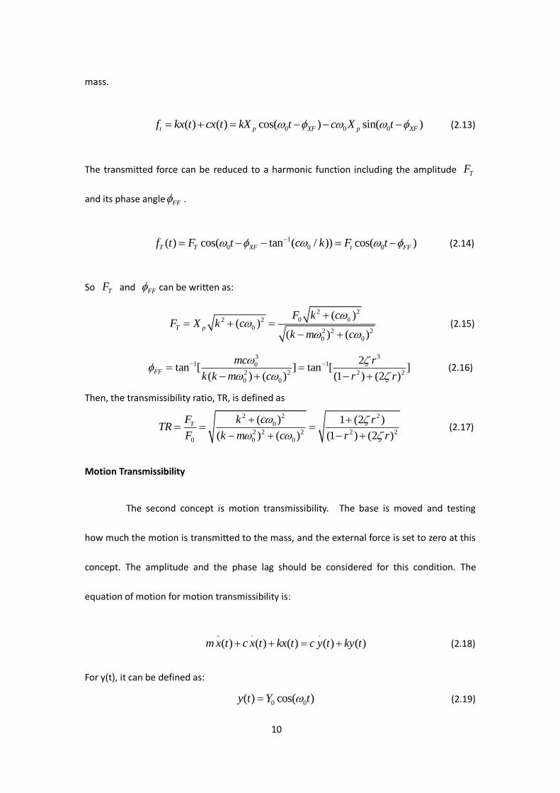
10
mass.
0 0 0( ) ( ) cos( ) sin( )t p XF p XFf kx t cx t kX t c X t (2.13)
The transmitted force can be reduced to a harmonic function including the amplitude TF
and its phase angle FF .
1
0 0 0( ) cos( tan ( / )) cos( )T T XF t FFf t F t c k F t (2.14)
So TF and FF can be written as:
2 2
0 02 2
02 2 2
0 0
( )( )
( ) ( )T p
F k cF X k c
k m c
(2.15)
3 31 10
2 2 2 2
0 0
2tan [ ] tan [ ]
( ) ( ) (1 ) (2 )FF
mc r
k k m c r r
(2.16)
Then, the transmissibility ratio, TR, is defined as
2 2 2
0
2 2 2 2 2
0 0 0
( ) 1 (2 )
( ) ( ) (1 ) (2 )
Tk cF r
TRF k m c r r
(2.17)
Motion Transmissibility
The second concept is motion transmissibility. The base is moved and testing
how much the motion is transmitted to the mass, and the external force is set to zero at this
concept. The amplitude and the phase lag should be considered for this condition. The
equation of motion for motion transmissibility is:
.. . .
( ) ( ) ( ) ( ) ( )m x t c x t kx t c y t ky t (2.18)
For y(t), it can be defined as:
0 0( ) cos( )y t Y t (2.19)

11
where the right side of Eq.(2.18) can be converted to :
.'
0 0 0 0 0 0 0( ) ( ) cos( ) cos( ) 'cos( )YYc y t ky t c Y t kY t Y t (2.20)
Through the property of the orthogonality for sine and cosine, the amplitude and the phase
lag is:
' 2 2
0 0 0( )Y Y k c (2.21)
' 1 0tan ( )YY
c
k
(2.22)
Eq. (2.6) is the form for the motion in steady state.
Then put (2.6) and (2.20) into the (2.18), the new equation becomes:
2 ' '
0 0 0 0{ [( )cos( ) sin( )] cos( )}cos( )XX XX YYXp k m c Y t (2.23)
2 ' '
0 0 0 0{ [( )sin( ) cos( )] sin( )}sin( )XX XX YYXp k m c Y t (2.24)
Xp and XX can be gotten:
2 2'0 00
2 2 2 2 2
0 0 0 0
( )
( ) ( ) ( ) ( )
Y k cYXp
k m c k m c
(2.25)
3 31 10
2 22 2 2
0 0
2tan [ ] tan
(1 ) (2 )( ) ( )XX
mc r
r rk m c
(2.26)
So the output displacement over the input displacement transmissibility is:
2 2 2
0
2 2 22 2 20 0 0
( ) 1 (2 )
(1 ) (2 )( ) ( )
Pk cX r
TRY r rk m c
(2.27)
It is equivalent to measure the transmissibility for any two displacement or
acceleration response variables. And the equivalence for the transmissibilities of various
response variables is very important since acceleration is easier to measure than

12
displacement or velocity due to the inertial frame that can be used to measure acceleration.
Acceleration is a good motion measurement since the Fourier transform only can be used in
the environment at steady state. Furthermore, regardless of the excitation level, the
magnitude and the phase lag of the transmissibilities will keep the same in the forced linear
system.
Section 3 A technique Way to analyze and display the mechanical resonance
Analyzer
Figure3 is a type of analyzer to test the transmissibility of the MEMS device.
Figure 3 Hp 35665 Dynamic Signal Analyzer
There are some tools to test the transmissibility of a mechanical system. For an
example, the Hp 35665 Dynamic Signal Analyzer, as shown in Figure 3, is produced by Agilent
Technologies and is used to analyze the results of the mechanical system. This analyzer has

13
two input signals and the maximum resolution of the signal is 800 lines, the other options for
the lines of resolution are 100, 200 and 400 lines. The analyzer has one channel at the
frequency of 102.4 KHz which has spans from 102.4 KHz to 0.019531Hz, two channels at 51.2
KHz which have spans from 51.2 KHz to 0.097656 Hz. The average real time bandwidth is
above 12.8 KHz. The graphs can be observed both in the time and frequency domains. It
has a source output port, and this port can provide different kinds of signals, such as random,
burst random, pink noise, sine, burst chirp, swept-sine, and arbitrary signals. Furthermore,
the small shaker can use the dynamic analyzer to control the power amplifier. It can be used
for different types of measurement, such as linear spectrum, power spectral density, time
waveform, PDF, CDF, frequency response, and cross-spectrum. For the measurement rate, it
has a 401 point FFT to display, and the fast average for one channel mode above 33
averages/ second (typical) and for one channel it is above 15 averages/ second (typical). Its
input noise level is 140 dbVrms/(sq.R)Hz when the frequency is above 1280Hz and -130
dbVrms/(sq.R)Hz when the frequency is 160Hz to 1.28 kHz. The full span FFT noise floor for
the analyzer is less than -76db, and it is -85db in the typical condition. The gain accuracy of
the FFT Cross-Channel is 0.04 db (0.46%) and the phase accuracy of the FFT Cross-Channel
is 0.5 degree. The minimum frequency resolution for the analyzer is 122μHz. This
machine has very good performance, it has low noise inputs and high speed computation
ability, but it is a very complex design and requires a high cost to purchase it.
Bode figure
Figure 4 is an example of Bode figure. A Bode figure is a graph to display the

14
property of the system frequency response, using a log-frequency axis, as a transfer function.
The Bode magnitude figure (in decibels) is the frequency response gain and the phase (in
degrees) response is the frequency response phase shift. A Decibel is a not a number, it is a
ratio relationship of two number using a logarithmic scale.
Figure 4 Bode Figure
The decibel is used to express the magnitude axis by the 20 log rule. 20 log rule
means the value is 20 times the value of the log of the amplitude. Every tickmark of the axis
represents a 10 times power. Because each unit is a power of 10, the decade is referred in
the figure.
For the 1( ) tan ( )X
T jR
Bode Gain Calculations
The magnitude for the transfer function T can be defined as:

15
2 2| ( ) |T j R X (2.28)
Where R is a real part, X is an imaginary part.
Because it is sometimes difficult to transfer a function from the “numerator/denominator”
to “real+ imaginary”, so it uses a fraction with denominator and numerator to defined it:
| |( )
| |
nn
mn
j zT j
j P
(2.29)
Where Zn and Pm are the breakpoints of the figure, at these points, in direction, they get the
largest change.
Gain can be calculated by converting both sides to decibels, and using logarithms:
20log( ) 20log( )n m
n m
Gain j z j p . (2.30)
Bode phase shift
Bode phase figures reflect the properties of the phase shift at each input
frequency and the Fourier Transform can account for its characteristics of the system. In the
“real + imaginary” form, the function is given as:
1( ) tan ( )X
T jR
(2.31)

16
Section4 Sampling and FFT
The Fourier transform is one of the most important methods to transform data
functions and sequences, to transform the time domain of the data to the frequency domain.
The Fourier transform is often used in the domain of linear system analysis, optics, antenna
studies, random process modeling, quantum physics, probability theory and boundary-value
problems, furthermore, and it can be used in the restoration of astronomical data
successfully.
Any periodic function and frequency can be written as a linear function made by
sine and cosine functions. This feature is called the Fourier series expansion of the function.
The FFT is a way to get such amplitude and frequency information for some functions and
sequences, which are not periodic.
Discrete Fourier Transform (DFT)
The DFT is to transfer the discrete periodic sequence f[k] in the time domain to
another discrete sequence F[j] in the frequency domain. K is an integer and N is the period.
The DFT can be defined as:
12 /
0
[ ] [ ]N
iki N
k
F j f k e
, 0≤j≤N-1; (2.32)
12 /
0
1[ ] [ ]
Niki N
k
f k F j eN
, 0≤k≤N-1; (2.33)
The sequence f[k] is a linear sequence of the N sinusoids, and it is the sum of 0e …
(2 / ) ( 1)N k Ne , (2 / ) ( 1)N k Ne and F[0], F[1]…F[N-1] are the coefficients of the sinusoids,

17
meantime the frequencies are j/N pre sample.
Sampling
Figure 5 Sampling Process
x(t) is a continuous signal that needs to be sampled and p(t) is an impulse train.
( ) [ ],k
p t t kT
(2.34)
As shown in the Figure 5, ( )px t is the new sequence that the data of this sequence equals
to the data of x(t) at the times of the sampling period, and other points are zero.
( ) ( ) ( ) [ ] [ ],p
n
x t x t p t x nT t nT
(2.35)
In certain conditions, a continuous signal can be represented by discrete sequences and this
method is sampling the data points from the periodic signal.
( )p j is the result of the Fourier transform for an impulse, it can be expressed as
2( ) ( )s
k
p j kT
, (2.36)
where
2 /s N (2.37)
Combining the (2.35) and (2.36), we have

18
1( ) ( ( ))p s
k
X j X j kT
(2.38)
Figure 6, 7, 8 shows the process of the sampling, they are X(t), P(t), ( )px t
respectively.
.
Figure6
Figure7

19
Figure 8
Figure 9 is an original signal. Figure 10 and Figure11 are two possible results when
it is reconstructed.
Figure 9
Figure 10

20
Figure 11
If the sampling frequency is s , it is at least two times higher than the highest
frequency of m , m is the original signal, and it is possible to reconstruct the signal from
the samples, and this fact is Nyquist’s Theorem, the Nyquist frequency is a sampling
frequency ωs=2ωm. If the condition is not met, what will happen is that the information of
the original signal will be lost. The duplications of the original signal‘s spectrum can overlap
the original one, and the spectrum of original signal will have the bogus signal and some
spectrum frequency will be lost, and Figure 10 displays the possible result. Furthermore, it is
impossible to reconstruct the signal from its sample. So the phenomenon that the useful
spectrum information is replaced by the bogus spectrum information is called aliasing. If the
frequency is larger than 2ωn, the signal information will be not lost, such as shown in Figure
11.
Fast Fourier Transform (FFT)
An FFT is a fast and efficient algorithm to compute the DFT. The DFT has a forward
DFT and an IDFT as follows:
DFT:

21
1
0
( ) ( )N
kn
N
n
X k x n W
, 0 kN-1; (2.39)
IDFT:
1
0
1( ) ( )
Nnk
N
n
x n X k WN
, 0 nN-1 (2.40)
The DFT computation is inefficient because it does not use the periodicity and symmetry
properties of the Twiddle factor NW . These properties are:
Periodicity property k N k
N NW W (2.41)
Symmetry property /2k N k
N NW W (2.42)
Considering the computation 2vN ,3
8W The N-point data FFT can be divided to 2 part N/2
– point data FFT f1(n), f2(n), according to the samples of x(n), these are,
1
2
( ) (2 )
( ) (2 1)
f n X n
f n X n
n= 0,1,.., N/2 -1; (2.43)
So the f1(n) and f2(n) are gained decimating x(n) through a factor of 2;
Decimation-in-time algorithm
1
0
( ) ( )N
kn
N
n
X k x n W
(2.44)
= 1 2( ) ( )K
NF k W F k
F1(k) and F2(k) are respectively the N/2 point DFTs of the f1(n) and f2(n).
F1(k) and F2(k) are periodic , and the period is N/2.
12 2
1 /2 2
0 0
1 2
( ) ( )
( ) ( )
N N
kn
N
n n
K
N
f n W f n W
F k W F k

22
So F1(k+N/2)=F1(k), F2(k+N/2)=F2(k). Since the factor /2k N k
N NW W
1 2( ) ( ) ( )k
NX k F k W F k , k=0,1,…,N/2-1 (2.45)
1 2( ) ( ) ( )2
k
N
NX k F k W F k , k=0,1,…N/2-1 (2.46)
it can be found that the computation of F1(k) needs 2( / 2)N complex multiplications, and
the same for the computation of F2(k). Moreover, computing 2 ( )k
NW F k needs the N/2
additional complex multiplications. So the total computation consume of X(k) is 22( / 2)N
+N/2= 2 / 2N + N/2 complex multiplications. So at first, it can reduce the number of
multiplications from 2N to 2 / 2N + N/2.
Then by computing N/4 point DFTs, it obtains the N/2 point F1(k) and F2(k)
1 1 /2 1( ) { (2 )} { (2 1)}k
NF k F f n W F f n , k =0, 1…, N/4-1; n= 0, 1,…, N/4-1 (2.47)
1 1 /2 1( ) { (2 )} { (2 1)}4
k
N
NF k F f n W F f n , k =0, 1…, N/4-1; n= 0, 1,…, N/4-1 (2.48)
2 2 /2 2( ) { (2 )} { (2 1)}k
NF k F f n W F f n , k =0, 1…, N/4-1; n= 0, 1,…, N/4-1 (2.49)
2 2 /2 2( ) { (2 )} { (2 1)}4
k
N
NF k F f n W F f n , k =0, 1…, N/4-1; n= 0, 1,…, N/4-1 (2.50)
The decimation of the sequence is repeated again and again, and the sequences can be
reduced to one point sequences. The computations of the decimation are performed v=
2logV N , when N= 2N. Thus, the total computation of complex multiplications for the
sequence is reduced to 2( / 2) logN N .The computation of complex additions is 2logN N .
The example is N=8, gets the computation of N=8 DFTs. It can be observed that the process is
performed through tree stages, the first step is to compute four two-point DFTs, the second
step is to compute two four-point DFTS, then one eight-point DFT.

23
Figure 12 is 3 stages decimation-in-time FFT, and Figure 13 display its details of
computation and Figure 14 shows basic computation of butterfly.
Figure 12 3-stages for 8-point FFT
Figure 13 8-point butterfly computation in the algorithm.

24
Figure 14 Basic butterfly computation in the decimation-in-time FFT algorithm
Decimation-in-frequency algorithm
Another important algorithm is the decimation-in-frequency algorithm, and it is
gained by using the approach of divide-and-conquer. At the beginning, the formula of DFT
two parts are spilt, one of which has the first N/2 data points and the second part has the
last N/2 data points.
( )X k( / 2 ) 1 ( / 2 ) 1
/2
0 0
( ) ( )2
N Nkn Nk kn
N
n n
Nx n Wn W x n Wn
(2.51)
Since /2 ( 1)kN k
NW ,
/2 ( 1)kN k
NW (2.52)
Then, it can be split to even-numbered samples and odd-numbered samples.
( /2) 1
/2
0
(2 ) [ ( ) ( )]2
Nkn
N
n
NX k x n x n W
(2.53)
( /2) 1
/2
0
(2 1) [ ( ) ( )]2
Nn kn
n N
n
NX k x n x n W W
(2.54)
If 1( ) ( ) ( )2
Nx n x n x n
2 ( ) [ ( ) ( )]2
n
N
Nx n x n x n W
( /2) 1
1 /2
0
(2 ) ( )N
kn
N
n
X k x n W
(2.55)

25
( /2) 1
2 /2
0
(2 1) ( )N
kn
N
n
X k x n W
(2.56)
For this algorithm, the FFT needs about 2logN N complex additions and 2( / 2) logN N
complex multiplications. The computation can be repeated by the decimation of two
N/2-point X(2k) and X(2k+1), and it needs v= 2log N stages to decimate, and each stage has
N/2 butterflies.
Figure 15, 16, 17 displays the decimation-in-frequency FFT algorithm.
Figure 15 the first stage for the 8-piont the decimation-in-frequency FFT algorithm.

26
Figure16 8-piont the decimation-in-frequency FFT algorithm.
Figure 17 Basic computation in the decimation-in-time FFT algorithm

27
Chapter 3 The tools used for design.
Section 1 Microcontroller
Introduction to Microcontroller
A microcontroller is an integrated circuit similar to a small computer, containing
memory, a processor core and input/output peripherals. In contrast to microprocessors
designed for personal computers, they are often used for embedded applications.
Moreover, microcontrollers sometimes are designed into automatically
controlled devices and products, such as office machines, engine control systems, and power
tools. To make it lower cost to more devices and microcontrollers, the size and the
calculation of the speed of the microcontroller are considered more. One type is designed
for 4-bit words and has clock frequencies of 4 KHz. It has low power consumption and is used
for retaining functionality when waiting for interrupts. The other type is for
performance-critical roles, like digital signal processing. A microprocessor is the core of the
microcontroller.
The first microprocessor was developed by Intel in 1971. it was a general
purpose 4-bit Intel 4004 microprocessor, but because of the system cost, it was impossible to
get the external chips to make it become a working system. Since the early 1970s, the
capacity of microprocessors has increased a lot and it has followed Moore's law. During the
1990s, erasable and programmable ROM for microcontrollers, such as flash memory,
appeared and occupied in the electronics market. With the help of electrical signals, this kind

28
of microcontrollers can be programmed, erased and reprogrammed. Nowadays, besides
general purpose microcontrollers, unique microcontrollers have started to be used in a
variety of areas, such as automotive, communications and lighting, and some
microcontrollers, like the PIC and the AVR, are becoming smaller, sleeker and more powerful.
Microcontroller cost plummeted a lot, and some inexpensive 32-bit microcontrollers are $1
USD, and some cheap 8 bit microcontrollers are $0.25 USD.
Introduction to the Stm32f407
The Stm32 is a type of 32-bit microcontroller integrated circuit made by
STMicroelectronics. The microprocessors of this family are based around a 32-bit ARM
processor core, like the Cortex-M4F, the Cortex-M0,and the Cortex-M3. Internally, each
microcontroller has certain parts, the processor core, flash memory, static RAM memory, a
debugging interface, and various peripherals. The Stm32 F4-series is the STM32
microcontroller family that uses an ARM Cortex-M4 core. They also have the advantage that
they support DSP and floating point instructions. It has a 64K CCM static RAM, a full duplex
I2S, faster ADCs, and an improved real-time clock.
The Stm32f407, as shown in Figure 17, is designed for industrial and medical
applications which require a high level of performance and integration.

29
Figure 17 Stm32f407
The microprocessor of this microcontroller is the Cortex-M4 core running at 168
MHZ. At 168MHZ, with 0-waite states of the ST’s ART Accelerator, it sends 210 DMIPS/566
Core Mark performances by Flash memory. Furthermore, the current consumption can be as
low as 238µA/MHZ.
The connectivity of the STM32F407 is rich, since it can connect a CMOS camera
sensor via an 8 to 14-bit parallel camera interface and can feature Ethernet with IEEE
support.
It has 2 USB OTG; one of these is supported by HS. It has 15 communication
interfaces, 6x USARTs, 3x SPI, 3x I2C, 2x CAN and SDIO). For the timers, it has 17 timers which
are 16 and 32-bit having the ability to run at 168MHZ. Furthermore it uses a flexible static
memory controller which can support SRAM, PSRAM, Compact Flash, NOR and NAND

30
Memories, and the memory range is extendable.
The STM32F407 product line has192 Kbytes of SRAM, from 512Kbytes to 1 M
Byte of Flash and from 100 to 176 pins in the packages.
The architecture of the STM32F407
The 32-bit multilayer AHB bus is used in the main system, as shown in Figure 18,
and it has 8 masters; they are the Cortex-M4 with an FPU core D-bus, I-bus and S-bus, DMA 1
memory bus, DMA2 memory bus, DMA2 peripheral bus, Ethernet DMA bus and USB OTG HS
DMA bus. Furthermore, it has 7 slaves; they are the Internal Flash memory ICode bus, the
Internal Flash memory DCode bus, the Main internal SRAM1 (112KB), the Auxiliary internal
SRAM2(16KB), the AHB1 peripherals, the AHB2 peripherals and the FSMC.
Embedded Flash memory interface
For the flash memory interface of Stm32f407, as shown in Figure 19, it manages
CPU AHB I-Code and D-CODE connects to the Flash memory. It has program and erase flash
memory operations and also has mechanisms of read and write protection. By the help of
instruction prefetch and cache lines, it can improve code execution.

31
Figure 18 System architecture for STM32F407
Figure 19 Flash memory interface connection inside system architecture

32
ADC of STM32F407
The function of the ADC is to successive approximation convert analog-to-digital,
and it is 12 bit in the STM32F407. It has 19 multiplexed channels, 16 of them to measure
signals from an external source, 2 of them to measure signals from inside the source and one
for the VBAT channel. The channels have 4 conversion modes; they can be run in single, scan,
continuous or discontinuous mode. After the conversion, the result of the ADC is stored in
the 16-bit data register which is left or right-aligned.
For the ADC, it has an External trigger option and it can be used in both regular and
injected conversions.
Multi ADC mode
For the stm32F407, it can use two ADCs or more, the Dual and Triple ADC modes
can be used. DMA has three modes to request in ADC.
DMA mode1: the ADC-converted data as a half-word is transferred on each DMA request.
As an example: on the first request, ADC 1 data is transferred, and on the second request
ADC2 data is transferred and so on.
In DMA mode 2; two ADC-converted data items can be seen as two half-words and they can
be transferred as a word.
As an example: in Dual ADC mode, on the first request both ADC1 and ADC2 data can be

33
transferred.
DMA mode 3: it is similar to DMA mode2; the difference in this type of DMA requests is that
two ADC converted data packets as two bytes are transferred.
Timers of the STM32F407
TIM2 to TIM5: general purpose timers.
These two timers are made by a 16-bit auto reload counter that is driven by a programmable
prescaler. They can be used for many purposes, like input capture, output compare, PWM
generation, and one-pulse mode output. By the timer prescaler and controller prescaler, the
waveform periods and pulse lengths can be modulated in several milliseconds at most.
Tim1&Tim8: Advanced-control timers.
These have almost the same function as a general purpose timer. Besides these functions,
they have some advanced function. They can use external signals to the control timers and
to interconnect several timers by a synchronization circuit.
They have a repetition counter to update the registers of the timer after the counter gives
the number of cycles.
They can put the timer’s output into a reset state or into a known state by breaking the
input.
TIM6&TIM7 Basic timers

34
They are the timers that have a 16-bit auto reload upcounter and a 16-bit programmable
prescaler.
For this purpose, they can be used for a time-base as generic timers. Furthermore, it can be
used for a DAC; they can be used in the procedure of digital-to-analog conversion. They can
drive this conversion by their trigger outputs.
Section 2 GUI
A GUI is a family of user interfaces that allow the users to easily communicate with
electronic devices by the visual indicators and graphical icons. Usability is a design discipline
for the GUI to make the design of a stored program efficient and easy of use. User-centered
design is the discipline to make the visual language fit for the task well.
The visual widgets are manipulated by the user to make the interactions
appropriate for the data they hold. The widgets can be chosen to support the actions when
the user interacts with the information. The GUI is customized, because it has a flexible
structure so that the interface is independent and is not connected to the application directly.
The user can easily change the interface and get what they want. It has some applications,
such as airline self-ticketing and check-in, automated teller machines, self-service checkouts
in a retail store and the information kiosks in a public space.
Section3 VCP
USB

35
Universal Serial Bus (USB) is designed to make different peripherals be connected by a
standardized interface. It provides a fast, expandable, low-cost, hot-pluggable, bi-directional
hardware interface where the computer users can easily plug many peripheral devices to the
USB and make the devices automatically configure. The USB can make the user connect a big
range of peripheral devices by a single connector type, such as, mice, keyboards, printers,
mass storage devices, scanners, telephones, digital still-image cameras, modems, audio
devices, video cameras to a computer. USB is not mapped into computer I/O address space
and does not use DMA channels and IRQ lines, so it does not consume system resources
directly. Memory buffers of the USB system software are the only system resources
consumed by a USB system.
VCP
COM ports provide an easy way for embedded systems and PCs to exchange
information. The traditional way for a COM port to operate on a PC is by using an RS-232
serial port. Recent PCs sometimes skip the function of RS-232 because of the application of
USB. A USB device can be used as a VCP that the application can access using the SerialPort
class of .NET’s with the right firmware.
When USB is used as a VCP, it is an interface that can give applications access to a
USB device like a built-in-serial port. There are many functions of USB VCP that can be used
as bridges to convert between RS-232. But sometimes a VCP does not need a serial interface.
Some VCPs convert between a parallel interface and USB. Or a VCP just reads and stores data
from a port of an on-chip analog to digital converter and sends it to a PC by USB.

36
Chapter 4 Design principle
From figure 20, the project is made up of 4 steps. They are ADC, a modified
FFT algorithm, VCP and a GUI which are designed and connected together to test the
transmissibility of a MEMS device.
Figure 20 Process for the design
The first step is ADC. ADC will happen when the signal from the MEMS device is
transmitted to the Stm32f407. The type of signal is an analog signal. Analog signals cannot
be analyzed by the computer, because it has infinite resolution. ADC is a process that can
convert continuous signals to digital numbers to represent the signal’s amplitude. Two ADC
channels are used to transfer the input and output signals.

37
The second step is the use of a modified FFT algorithm to transfer the time
domain of the signal to the frequency domain. An FFT is an algorithm to calculate the DFT
quickly. The DFT is used to convert the function from time domain to frequency domain.
Through the algorithm, it can calculate the value of the amplitude of output data and input
data and then the ratio of the output to input will be computed. Since the existence of the
calculation error and the limitation of the calculation, it will produce noise around the peak
and also it will produce white noise over the entire frequency domain, so it will need to
improve performance by digital filtering.
The third step is to set VCP. VCP is used to transfer the result from the
microcontroller to the personal computer. The microcontroller has the function of the Virtual
Com port; it can cause the USB2.0 to perform as a COM port, and it can get higher speed
than an ordinary COM port.
The last step is the design of the GUI. After the PC receives the data from the
microcontroller, the visual studio is used as a GUI in the project. After the data is transferred
by the VCP, It uses Windows Forms to create and design the data display figure. It uses the
thread way to simplify the program and to prove the real-time of the figure. At last the final
result of the MEMS device will display in the PC correctly. And the transmissibility of the
MEMS device will be displayed dynamically.

38
Figure 21 is the ADC structure of STM32f407.
Figure 21 ADC Structure
Section1 The configuration of the ADC
Choosing ADC Channels
The test of transmissibility needs two signals to test and ratio, one is defined as the
input signal and the other one is defined as the output signal. For the convenience of the
configuration, the process needs the two ADC channels to convert the data at the same time.
For the stm32f407, as shown in Figure 21, it has three ADC modes, ADC1, ADC2 and ADC3,
and each of them has 16 channels that can transfer the data to the converter.

39
For the process, two channels of ADC 1 are selected to transfer the data.
Table 1 shows the configuration for each ADC.
ADC1 ADC2 ADC3
Channel0 PA0 PA0 PA0
Channel1 PA1 PA1 PA1
Channel2 PA2 PA2 PA2
Channel3 PA3 PA3 PA3
Channel4 PA4 PA4 PF6
Channel5 PA5 PA5 PF7
Channel6 PA6 PA6 PF8
Channel7 PA7 PA7 PF9
Channel8 PB0 PB0 PF10
Channel9 PB1 PB1
Channel10 PC0 PC0 PC0
Channel11 PC1 PC1 PC1
Channel12 PC2 PC2 PC2
Channel13 PC3 PC3 PC3
Channel14 PC4 PC4
Channel15 PC5 PC5
Channel16 Temp sensor
Channel17 REFV
Table 1 ADC configuration
The mode ADC3 is selected in the process. For the channel selection, channel 12
and Channel 13 are selected and PC2 and PC3 are configured for these two channels, as
shown in Table 1.
In the process ADC, DMA plays an important role for the transfer of the data.
DMA allows the data transfer between memory and peripherals or memory and memory

40
without the help of CPU action. It can provide higher speed to the microcontroller. The
Stm32f407 has two DMA controllers and each of them has 8 streams. Each stream can be
used to manage memory access requests from for one or more peripherals. Up to 8 channels
can be used for each stream. For the DMA 1, there is no stream to use for the ADC.
And for DMA2 selection:
For the ADC1: Stream0 Channel0, Stream 4 Channel0
For the ADC2: Stream2 Channel1, Stream 3 Channel1
For the ADC3: Stream0 Channel2, Stream 1 Channel2
In the process, the DMA2 stream0 Channel2 is used.
Sampling frequency
Sampling frequency for the ADC is also important and the sampling time is
programmable. The ADC samples the voltage of the input as ADCCLK cycles that will be
modified. For this ADC process, it needs the sampling time as long as possible and to make
the sampling rate as fast as possible, since the figure requires the frequency resolution as
small as possible, and the detail of the figure can be observed easier.
So the calculation to get the sampling frequency for the process:
The APB2 bus is used for the process

41
The clock is 84MHz
The prescaler for the clock is 8,
Tcov= sampling time + 12cycles = 480 +12= 492cycles
So the ADC sampling frequency is 84MHz/8/492=21.3khz.
Moreover, a sampling frequency of 21.3 KHz cannot satisfy the requirements for
the frequency resolution. Another way to reduce the sampling rate is needed. The way to
reduce the sampling rate is to sample 8192 points each time, and get out one point of eight
points to get 1024 for input signal channel, and other one point of eight points for output
signal channel. And the sampling rate should be about 2.7 KHz at this condition, because
the time to get 1 point becomes 8 times slower than before.
And for the ADC process, it does not use an external trigger, but use the software
to trigger the ADC.
Working principle for ADC
For the process, 1024 points data will be used in the FFT one time to get the
frequency time, and the ADC needs to sample 8192 points each time. The process uses the
multichannel continuous conversion mode. For this mode, the process can configure the
sequence of the ADC channels successively, and restarts at the first channel after the last
channel conversion. So Channel 12 of ADC3 is configured to transfers one input data at first,
after that, channel 13 of ADC3 is configured to transfer one output data, and the process is

42
restarted by this way.
Figure 22 displays the working principle of the Multichannel of ADC. The buffer
size for the DMA is 8192, with all the data from the converter stored in it, the odd 16-bits is
for the data from Channel 12 and the even 16-bits is for the data from the Channel 13.
Figure 22 Working Principle for the Multichannel of ADC

43
The timer design
The Figure 23 displays the flow chart of the timer in the process of ADC.
Figure 23 Timer in the process of ADC
For the timer design, the function of the timer is to trigger the interrupt
where the FFT algorithm for the design is calculated. The timer used for the trigger in the
design is TIM2. In the interrupt, the stm32f407 needs to close the function of ADC to ensure
that the ADC does not work during the algorithm calculation. At the end of the interrupt, the
function of the ADC will restart. The Timer period for the configuration is 65535 and its
prescaler is 4199; so the period time is designed:
((1+TIM_Prescaler )/84M)*(1+TIM_Period )= 4200/84M*65536=3.28s

44
At each 3.28s, the program will enter into the timer interrupt.
Section2 Modified FFT algorithm
The first part for the Modified FFT algorithm is a 1024 points FFT calculation.
For the stm32f407, the Cortex-M4 core has the ability of FPU single precision,
which can support all data types and data processing instructions of ARM single precision; so
the microcontroller can be used for complex calculations like the FFT. Furthermore, it has a
DSP library which has a rich set of DSP instruction to support complex calculations. For the
process, the FFT can be solved by the DSP library of the Stm32f407, and it accomplishes this
by way of a Radix-4 Decimation in Frequency algorithm. It is a floating point function process
written in the C language. In the FFT process, one FFT is calculated and the other FFT is
calculated next. Two 1024 point FFTs require high speed calculation ability from the
microcontroller. Without the use of the DSP library, it would be too difficult to finish so
complex of a calculation in 3s with the Stm32f407. Since DSP has a strong ability of
computation, it can easily finish 1024 points FFT within 4s, and it can fit for the design of the
timer. The DSP library can help the microcontroller reach this goal easily and its calculation is
lower than 2s actually. The DSP library not only has the function for the FFT, it also has the
function for getting the absolute value of the complex number, After the FFT, both ways get a
1024 complex number and all these complex numbers are sent to the DSP function to get the
absolute value. And after these steps, the value from the output signal and the value from
the input signal in the frequency domain are obtained by the microcontroller.
For the FFT used in this research, it needs to do a 1024 point one time FFT. To make

45
the frequency resolution as small as possible, it samples 8192 points each time and gets out
one point from each eight points each time. The frequency resolution in the frequency
domain is related to the sampling frequency. The original sampling rate for the ADC is 21.3
kHz. As mentioned before that the sampling rate needs to be as low as possible, the
sampling points for each ADC time are 8192 and it is 8 times than the points used for each
channel FFT, thus the sampling frequency will be reduced by 8 times. So the sampling
frequency for this time should be: 21300/8=2.7KHz and the frequency resolution will
be2700Hz/1024=2.6Hz. This frequency resolution is enough to reflect the property of the
transmissibility in the frequency domain.
Before, when the magnitude value is sent to the GUI, it will produce two kinds of
noise. One kind is from the ADC process; it exists in the total frequency domain by the term
of white noise. For this noise, an noise filter can be used to reduce it and it is easy to reduce.
The other kind is from the FFT calculation, since the FFT can’t display infinite
frequency points in the frequency domain because of the limitation of the calculation, and
the energy of the point that does not exist in the domain frequency will affect the point
around, it and this kind of noise will exist around the peak. For reducing this noise, an
averaging filter is used to cancel the noise and it is designed in part of the GUI,
For the process of transmissibility, it focused more on the amplitude in the
frequency domain. But phase shift also can be obtained during the process. The phase angle
of the complex number is y=a+bi. A and b can be positive or negative, thus to get the phase
angle of y, assume k= arctan(b/a)*180/ π; it has 4 different situations. If a>0, b>0, y=k; if a>0,

46
b<0, y=k; If a<0, b>0, y=k+180; If a<0, b<0, y=k-180. Then, the phase shift is the phase
difference between the phase angle of the input and output signals. When the figure is
displayed, the change in the phase shift can be displayed dynamically also.
Section3 VCP Design
After downloading the VCP driver for the Stm32f407, USB2.0 can be used as a COM
port to exchange the data between the microcontroller and the PC.
With the help of the VCP driver for the STM32, the function of VCP can be started.
Actually, the core to operate VCP is similar with that of an ordinary COM port. The result of
the calculation of the board is sent to the PC by USB. When the data is received by the PC,
the data needs to be read and operated on later. For the transmission of VCP, one data needs
to be broken into several bytes, since the unit transferred in the USB is one byte.
Furthermore, to reduce the possible errors during the USB transmission or the storage, the
checksum for the data that the PC received is important. For this step, after the data is
unpacked, the sum of these bytes is gained and the result is appended as extra bytes. After
all the bytes have been received by the PC, their sum will be computed again and compared
with the sum computed in the microcontroller, and then all the data will be packed in bytes.
If the result of the comparison is unequal, the error will be detected. This can prove the
stability for the function of VCP. Furthermore, since more than 2100 bytes need to be
transferred, the process size of the buffer for the USB transfer to the PC is set 4096 bytes, so
it can prove that all of the useful bytes are transferred one time and make the process in real
time. The speed of the USB transformation is tested by the software, and is about 200kb/s. It

47
is much higher than the ordinary COM port. The high speed of transmission is a key step to
prove the property of real time for the test of transmissibility.
Section 4 Design of GUI
The Visual Studio is used to display the transmissibility figure real time. Windows
is the application programming interface to operate the data which can provide access to the
Microsoft Windows interface elements through the way of packing the Windows application
programming interface in managed code.
There are three parts for the code. They are Program.cs file, Form1.cs file and
Form1.Designer.cs file. Program.cs is the starting point for the program and the code Form1
consists of Form1.cs and Form1.Designer.cs file. Form1.Designer.cs contains the code to
design the figure which is generated when the components are dragged to the form using
toolbox. Meantime, Form1.cs is the place where the logic function is designed by the code.
Figure 24 displays main steps of GUI

48
Figure 24 process of GUI
Process of GUI
The code is process oriented, as shown in Figure 24. At first, the serial port is
configured. The class SerialPort is used for the data received and read. During the process,
the data will be checked by way of checksum and processed using averaging to reduce noise
in the figure drawn by the processed data.

49
Thread to draw the figure
The interface needs to display the frequency domain real time data dynamically
and the data size is very big each time. It is possible to be stuck in the process when the
interface updates the data. During the process, receiving data by Serialport will create a new
thread, function of this.invoke can be seen as a delegate to update the interface in this
thread. Threading is the ability to create an application that uses two or more thread
executions. Thus one thread for the GUI process is to get the data transferred by the Virtual
COM port at first and the second thread is to display the frequency domain real time data
after unpacking the data. The function of the this.invoke is to call the method to update the
points in the frequency domain.
Design of the Interface
For the Interface, a bitmap is used to draw the picture, as shown in Figure 25.
For computer graphics, a bitmap stores a binary image in the domain which is a rectangle
and the pixel in an image is either white or black. The bitmap consists of the figure of the
magnitude and the figure of the phase shift. The data of the magnitude and the data of the
phase shift will be sent to the bitmap, respectively. The GUI has the buttons to operate the
autoscale function for the figure of the magnitude. The autoscale function is used to make
the peak of the magnitude seen clearly by adjusting the scale of the value. It can be 2 times,
10 times and 25 times larger than the true value so that the figure can be observed easily. In
the figure, the coordinate values need to be changed by the values of frequency resolution
so that the frequency at the n points can be known. The frequency resolution is 2.6 Hz,

50
obtained from the section of the Modified FFT and it is low enough to reflect the property of
the frequency domain. When the frequency resolution is obtained, each interval in the
frequency domain in the figure will be 2.6Hz. The first point in the x axis should be 2.6 Hz
and the second point should be 5.2 Hz, and so on, and the largest frequency in the frequency
domain of the figure for the value can be more than 1000 Hz. For the phase shift, the range
of the phase is from -π to π.
Figure 25 Design of the interface
Writing out the data
The value of the transmissibility in the frequency domain will be written out
to a file. The class StreamWriter is used to write out data real time. Every 4 seconds, the data
can be written out one time, and the data written out last time can be used to draw a

51
professional figure in MATLAB or used for other work later.
Filtering noise
Furthermore, the GUI uses the averaging filtering to filter the noise of the peak, as
shown in Figure 26.
Figure 26 Flow chart of filtering noise
The method is easy to understand. First, after getting five times of data for each point in the
frequency domain, the maximum and minimum values of this data will be calculated and
canceled, and the average value of the remaining three values will be gotten. When the
average of the next five data points is obtained in the same way as before, it will be added to

52
the first average and the new average value can be gotten. Then when the average of the
third five data comes in, it will be added to the previous sum, and the new average is divided
by three to get the new overall average value. For the N average, it will be added to the
previous sum and then the new average value can be gotten, and the previous sum is N
times the value of the previous average. The white noise exists randomly, the technique for
canceling the maximum and minimum values can eliminate the sudden noise in the
frequency domain and averaging can reduce the white noise little by little meantime.
Reset function
In the research, the reset function is also set by the design. If the environment is
changed, after the reset button is pressed in the interface, the figure will restart again. The
function of reset can help the figure display the change clearly.

53
Chapter 5 Test
Section 1 Test by function generator
Test the correctness of ADC
To prove the correctness of the ADC configuration, an oscilloscope is used to test it
and the DAC process needs to be configured as well. It is the reverse process of ADC, since it
can convert a digital data to analog data again. Two ADC channels and two DAC channels are
used to recover a certain frequency wave. In the test of the configuration of ADC, only one
channel of ADC connects the input signal, which is from a function generator. When 1000
points were sampled, the 50Hz wave can be recovered successfully. It means the function of
ADC runs well. Figure 27 displays the function generator and oscilloscope to test ADC and
DAC.
Figure 27 Oscilloscope and Function generator.

54
Test the correctness of FFT
The function generator is also used to check the correctness and stability of the
FFT. This time, only one signal is sent by the function generator. The input is a sinusoidal
wave which has a certain frequency. So after the signal is processed by the design, besides
the DC component, it will appear as a high peak at a certain frequency with energy at other
frequencies being relatively low. After the check, the FFT can be used in the next step.
Simulate mechanical system
The function generator system is relatively simple compared with a mechanical
system and they will have the same feature with the phenomenon when testing the resonant
frequency, since a function generator can simulate the resonant frequency of a mechanical
system. If the fault is found during the test with a function generator, it is easy to correct.
Since for the design, one ADC input is for the Output signal and the other ADC
input is for the Input signal, two signals need to be produced by the function generator.
Because to find the mechanical resonance is to find the ratio of output and input, so for the
function generator, the circuit is connected to create the condition that the two signals have
the same frequency, but different amplitudes. After these two signals are processed by the
design, the peak in a certain frequency should be observed in the figure. To make the signals
the same frequency, these signals should be made by the same function generator. By using
a circuit, the amplitude of the signal A is 15 times greater than the amplitude of signal B, and
they have the same frequency. For an example, if the function generator is set to a certain

55
frequency signal, such as 199 Hz, and the output and input of the stm32f07 will be set to 199
Hz but with different amplitudes.
Figure 28 is the circuit to help to test the correctness of the design using the
function generator. There are 15 identical resistors connected in series in the circuit, the
signal B is tested after the first resistance and the signal A is tested after the other resistors,
and the signal from function generator is set at the same position, so the signal A should be
15 times bigger than Signal B. In the simulation by function generator, signal A can be seen as
output signal and signal B can be seen as input signal.
Figure 28 Circuit to verify the accuracy of the design by using function generator

56
In Figure 29, the peak is at 199 Hz, the amplitude is at 15, but in the other points of
the domain frequency, noise clearly exists.
Figure 29 The Original Result
During the test, since the noise around the input information or output information is much
smaller than mechanical resonance, but the ratio is close to or a little smaller than the
mechanical resonance, so the noise in the transmissibility figure can be eliminated by
eliminating the noise in the input information and the output information. If the input value

57
or output value is less than a set threshold, the ratio of the output to input can be set to 1,
which means that the input value equals the output value if there is no interference from the
noise. This threshold should not be too high to mask the useful information for the
transmissibility. Through adopting this thresholding technique, all the noise around
mechanical resonance is eliminated. For real mechanical system, the input or output
information has no big difference with other spots noise, so the averaging filter introduced in
GUI section will make more contribution to the noise filter of the graph.
In the figure 30, the result is good by using the thresholding technique.
Figure 30 Result with noise filtering

58
Section 2 Assembling
Figure 31 Test system
For the mechanical system test, the core of the design is to test the transmissibility
of a MEMS device. Motion transmissibility of three samples is measured in the test. As
shown in Figure 31, an analyzer, a laser interferometer displacement measurement system,
and an electromechanical shaker are used for testing. An Hp35665A dynamic signal analyzer
is used to generate the excitation signals for the electromechanical shaker, such as a sine
wave for the shaker, and it can analyze the frequency response. The shaker is connected to
shake the sample and excite mechanical resonance. Two Polytec laser vibrometers are used
for measuring the displacement of the sample on the vibration system. The laser system

59
needs to measure the output and input displacement. Input is the displacement of the
holder, and output is the displacement of the sample. Analyzing the ratio of these two
displacements, the transmissibility of the system can be obtained. Then the signal gotten
from laser systems will transfer to a circuit to change the range of the voltage from -8V to 8V
to 0 to 3V with the help of a power supply, as shown in Figure 35, because it is the range of
voltage that can be received by the Stm32f407. Then the new signal is transferred to the
Stm32f407to compute the transmissibility to compare it with the results from the analyzer.
Polytec Laser Vibrometer System
The Polytec laser vibrometer is used to measure the displacement in a
non-contact way for this experiment, as shown in Figure 32. The fringe counter principle is
used for the displacement measurement for the system. The system uses two Polytec OFV
353 lasers which are held by two Manfrotto tripods, and point to the desired locations. Two
lasers can measure the displacement of the two different locations respectively .The system
also has two controllers for each laser, which provide power to the system and help to
convert the laser signal into an electrical signal. The output of each Polytec laser vibrometer
system is an analog signal which is proportional to the vibration amplitude in the measured
location. Then the signal can be observed on the oscilloscope or sent to a data acquisition
system to process, such as the HP 35665A dynamic signal analyzer.

60
Figure 32 Polytec Laser Vibrometer System
Measurement
Range
Full Scale
Output(Peak
to Peak)
Resolution Max
Vibration
Frequency
Max.
Velocity
Max.
Acceleration
μm/V Mm Μm kHz m/s G
20 0.32 0.08 20 1.6 20.000
80 1.3 0.32 20 1.6 20.000
320 5.2 1.3 20 1.6 20.000
1280 20.5 5 20 1.6 20.000
5120 82 20 20 1.6 20.000
Table 2 Parameters of Ploytec laser Vibrometer System
Electromechanical shaker
The electromechanical shaker used in the experiment consists of a V408 Shaker and a
PA 500L Amplifier. Vertical vibration is provided by the shaker and a set of fixtures that are
attached on the shaker and are ready for the transmissibility test, as shown in Figure 33. The

61
system also has a vibration control system which can generate time-domain signals
containing the required characteristics of frequency-domain and sends the signals to the
amplifier. The amplifier, as shown in Figure 34, will make the signal larger and then the
shaker will be driven by the powerful amplified signal with a larger voltage and current. After
the signal is processed by the controller of the Polytec laser vibrometer, it will be transferred
to the frequency-domain in the analyzer by the FFT transform.
Figure33 V408 Shaker and Fixture Table

62
Figure 34 PA500L
Figure 35 and 36 give the detail of the circuit used in the project.
Figure 35 Power supply and circuit to change the range of voltage of input signal.

63
Figure 36 Circuit of design
Section 3 Compared with the results from analyzer
The analyzer is used to produce the transmissibility figure on the PC. Three
different samples with different materials and different locations are used to test the
correctness of the design, as shown in Figures 39, 40, 41. Furthermore, the results after the
FFT are also written to a file by the GUI and used by MATLAB to draw a more professional
figure. Then the figures of the analyzer also will be exported and compared with the figures
of MATLAB. During the first time, the shaker is not used, but the laser system is used. The
peak also appears at 23Hz, as shown in Figure 37. It means the vibration system has its
original frequency response without any excitation; the frequency response results are due
to the fixture itself. Figure 38 is the figure made by MATLAB. Using MATLAB to get the figure
is more professional and can be compared with the figure from the analyzer clearly. Then

64
three different samples are used to test and verify the results of the design. They are put in
the fixture and use the laser system to measure the different locations of the sample.
Figure 37 and 38 display the transmissibility of the fixture itself without of the help
of the shaker.
Figure 37 One Peak at 23Hz in my interface.

65
Figure 38 One peak at 23Hz displayed in MATLAB
Figure 39, 40, 41 are the samples measured in the project.
Figure 39 The first sample to test

66
Figure40 The second sample to test
Figure41 The third sample to test

67
For the first sample, two peaks appear in the figure.
As shown in Figure 42, one peak is at 53 Hz, the other one is at 59 Hz, and the high
peak is close to 13 and the other one is close to 8. The shaker is used to excite the sample,
and the laser system is used to measure the transmissibility.
For the figure from the analyzer, as shown in Figure 43, it also has two peaks, and
the high peak is close to 10, the other one is close to 6.5. And from comparing the two
figures, the frequencies of the peaks are the same.
Figure 42 Two peaks at 53Hz and 59Hz displayed in MATLAB through the data of the design

68
Figure 43 Two peaks at 53Hz and 59Hz from Hp35665 analyzer.
For the second sample, there is peak at 135 Hz and its amplitude is close to 100, as
shown in Figure 44. The figure from analyzer also has a peak with an amplitude close to 100
at 135 Hz, as shown in Figure 45.

69
Figure 44 The peak at 135Hz displayed by MATLAB
Figure 45 The peak at 135Hz from Hp35665 Analyzer

70
For Figure 46, the new fixture is placed, and the different material is tested. For this
test, the peak is at 233 Hz, the amplitude is close to 20. The result from analyzer also has a
peak close to 20 at 233 Hz, as shown in Figure 47.
Figure 46 The peak at 233Hz displayed in MATLAB

71
Figure 47 The figure from Hp35665 analyzer at 233Hz

72
Chapter 6 Conclusion and future work.
In conclusion, the design shows the high performance of the STM32f407, includes its
computation ability and its DSP ability. The modified FFT algorithm is correct verified when it
is used to calculate the FFT in the project. The VCP works well and the data is transmitted
stably. The algorithm used after receiving data in the GUI successfully reduces the noise
effect during the transmission. The speed to display the figure is good enough to observe the
transmissibility. Through the averaging filter, the data received by the GUI can be refreshed
20s one time. Without averaging filter, the period is close to 4s. Furthermore, the data
displayed in the GUI can be collected and written out to analyze later. 3 different samples are
used to test the transmissibilities and the results of the design are uniform with the data
from the HP 35665 analyzer.
For future work, the design can be used in different applications to test the response
frequency. Not only for the MEMS device, but other useful applications can use this
technique to observe the resulting phenomenon, such as LC circuits and film deposition.
Furthermore, it can be embedded in some applications to perform its function.
For higher required calculation, the STM32f407 can be replaced by an FPGA, which has
better performance and faster speed, since it is focused more on parallel execution. For an
MCU, it needs more cycles to process in order to finish more work, but for the FPGA, it
doesn’t have this limit. The FPGA has a lot of FSM running all the time, it is only space limited
and is not time limited, and bigger an FPGA means a higher ability of calculation. With the
use of an FPGA, it can do a more precise FFT, and it can get better resolution. Furthermore,

73
more data and a better algorithm can be run in the FPGA, and the stability of the design can
be improved. With the high performance of calculation of the FPGA, its ability of real-time
will be better and the data received by the GUI can be refreshed faster.
For the noise present in the design, the design uses an averaging filter to reduce the
noise effect. But sometimes, if the transmissibility signal is very weak, the result won’t be
good, because the value of the noise will close to the value of the signal. For future work, to
prove its stability, better filter techniques can be tried. A hardware filter can be used in the
front of the design, or better filter algorithms can be used in the MCU or GUI, such as
adaptive-filtering, which can be used to reduce the noise effect during the process.
For the GUI design, the design can be designed more humanized and more functions can
be added so that it will be more easily used in future work.

74
References
1.Alan V. Oppenheim, Alan S. Willsky, S. Hamid , signal and systems(2nd section), Prentice
Hall, August 16, 1996
2.Chang Liu, Foundations of MEMS(second section), Prentice Hall, March 14, 2011
3.Marilyn Wolf, Computers as Components, Third Edition: Principles of Embedded
Computing System Design, Elsevier, May 23, 2012
4. Alan V.Oppenheim, Ronald W.Schafe, Discrete-time signal Processing(third section),
Prentice Hall, Jan 1, 2011.
5. Leonard Meirovith, Elements of vibration analysis(second edition), McGraw-Hill, 1986
6. Reference Manual for STM32F405xx/07xx, STM32F415xx/17xx, STM32F42xxx and
STM32F43xxx advanced ARM-based 32-bit MCUs.
7.R. Dean, G. Flowers, N. Sanders, R. Horvath, M. Kranz and M. Whitley, “Micromachined
vibration isolation filters to enhance packaging for mechanically harsh environments,” J.
Microelectronics and Electronic Packaging, Vol. 2, No. 4, 2005, pp. 223-231.
8.R. Dean, G. Flowers, R. Horvath, N. Sanders, S. Hodel, J. Hung and T. Roppel,
“Characterization and experimental verification of the nonlinear distortion in a technique for
measuring relative velocity between micromachined structures in normal translational
motion,” IEEE Sensors Journal, Vol. 7, No. 4, April 2007, pp. 496-501.
9.S.J. Kim, R. Dean, G. Flowers and C. Chen, “Active vibration control and isolation for

75
micromachined devices,” ASME J. of Mechanical Design, Vol. 131, Sept. 2009, pp. 091002-1 –
091002-6.
10.S.J. Kim, R. Dean, R.L. Jackson and G.T. Flowers, “An investigation of the damping effects
of various gas environments on a vibratory MEMS devices,” Tribology International, Vol. 44,
2011, pp. 125-133.
11.R.N. Dean, A. Anderson, S.J. Reeves, G. Flowers and A.S. Hodel, “Electrical noise in MEMS
capacitive elements resulting from environmental mechanical vibrations in harsh
environments,” IEEE Trans. on Industrial Electronics, Vol. 58, No. 7, July 2011, pp. 2697-2705
12.. Haoyue Yang, George Flowers, Thresholds of Axial Vibration Induced Fretting Corrosion
in Electrical Connectors, Holm Conference on Electrical Contacts (HOLM) , 2013 IEEE 59th
13. Zhang Haifeng, Zhao Jing, The design of RF data acquisition system based on
STM32 and FPGA, Multimedia Technology (ICMT), 2011 International Conference on, July
2011
14. Timothy James Johnson, Analysis dynamic transmissibility as a feature for structural
damage detection, Master thesis of Purdue University
15. James Potzick, Noise averaging and measurement resolution „or ‘‘A little noise is a good
thing’’,… Review of Scientific Instruments, Apr 1999
16. Saidi, A,Decimation-in-time-frequency FFT algorithm, Acoustics, Speech, and Signal

76
Processing, 1994. ICASSP-94., 1994 IEEE International Conference on, Apr 1994
17. Abumurad, A, Kyusun Choi, Increasing the ADC precision with oversampling in a flash
ADC, Solid-State and Integrated Circuit Technology (ICSICT), 2012 IEEE 11th International
Conference on, Nov 2012
18. Yaoliang Shi, Guangyu Zheng, Li Wu, Shusheng Peng, Design of a Multi-parameter
Measurement System, vol.12, No.4, April 2014, PP. 3118~3125

77
Appendix C code and C# code
(1) Main program for Stm32f407(ADC, DMA set)
#include "stm32f4xx.h"
#include "usbd_cdc_core.h"
#include "usbd_cdc_vcp.h"
#include "usbd_usr.h"
#include "usbd_desc.h"
#include "time.h"
#include "stm32f4_discovery.h"
#include <stdio.h>
#include <math.h>
#include <stdlib.h>
#include "arm_math.h"
#include "usbd_cdc_vcp.h"
#define ADC3_DR_ADDRESS ((uint32_t)0x4001224C)

78
#define ADC1_DR_ADDRESS ((uint32_t)0x4001204C)
__IO uint16_t ADC3ConvertedValue[8192];
float32_t Value1[2048];
float32_t Value2[2048];
void TimerInit(void);
void ADC3_CH12(void);
void TIM6_Config(void);
extern void FFT1_DAC(void);
__IO uint32_t ADC3ConvertedVoltage = 0;
__ALIGN_BEGIN USB_OTG_CORE_HANDLE USB_OTG_dev __ALIGN_END ;
/* Extern variables ----------------------------------------------------------*/
extern uint16_t VCP_DataTx(uint8_t* Buf, uint32_t Len);
/* Private function prototypes -----------------------------------------------*/
void Delay(__IO uint32_t nTick);
void Delay1( unsigned);

79
int main(void)
{
uint32_t i = 0;
USBD_Init(&USB_OTG_dev,
#ifdef USE_USB_OTG_HS
USB_OTG_HS_CORE_ID,
#else
USB_OTG_FS_CORE_ID,
#endif
&USR_desc,
&USBD_CDC_cb,
&USR_cb);
ADC3_CH12();
TimerInit();
void ADC3_CH12(void)

80
{
ADC_InitTypeDef ADC_InitStructure;
ADC_CommonInitTypeDef ADC_CommonInitStructure;
DMA_InitTypeDef DMA_InitStructure;
GPIO_InitTypeDef GPIO_InitStructure;
/* Enable ADC3, DMA2 and GPIO clocks ****************************************/
RCC_AHB1PeriphClockCmd(RCC_AHB1Periph_DMA2 | RCC_AHB1Periph_GPIOC, ENABLE);
RCC_APB2PeriphClockCmd(RCC_APB2Periph_ADC1, ENABLE);
/* DMA2 Stream0 channel0 configuration **************************************/
DMA_InitStructure.DMA_Channel = DMA_Channel_0;
DMA_InitStructure.DMA_PeripheralBaseAddr = (uint32_t)ADC1_DR_ADDRESS;
DMA_InitStructure.DMA_Memory0BaseAddr = (uint32_t)&ADC3ConvertedValue;
DMA_InitStructure.DMA_DIR = DMA_DIR_PeripheralToMemory;
DMA_InitStructure.DMA_BufferSize = 8192;

81
DMA_InitStructure.DMA_PeripheralInc = DMA_PeripheralInc_Disable;
DMA_InitStructure.DMA_MemoryInc = DMA_MemoryInc_Enable;
DMA_InitStructure.DMA_PeripheralDataSize = DMA_PeripheralDataSize_HalfWord;
DMA_InitStructure.DMA_MemoryDataSize = DMA_MemoryDataSize_HalfWord;
DMA_InitStructure.DMA_Mode = DMA_Mode_Circular;
DMA_InitStructure.DMA_Priority = DMA_Priority_High;
DMA_InitStructure.DMA_FIFOMode = DMA_FIFOMode_Disable;
DMA_InitStructure.DMA_FIFOThreshold = DMA_FIFOThreshold_HalfFull;
DMA_InitStructure.DMA_MemoryBurst = DMA_MemoryBurst_Single;
DMA_InitStructure.DMA_PeripheralBurst = DMA_PeripheralBurst_Single;
DMA_Init(DMA2_Stream0, &DMA_InitStructure);
DMA_Cmd(DMA2_Stream0, ENABLE);
/* Configure ADC3 Channel12 pin as analog input ******************************/
GPIO_InitStructure.GPIO_Pin = GPIO_Pin_2|GPIO_Pin_3;
GPIO_InitStructure.GPIO_Mode = GPIO_Mode_AN;

82
GPIO_InitStructure.GPIO_PuPd = GPIO_PuPd_NOPULL ;
GPIO_Init(GPIOC, &GPIO_InitStructure);
/* ADC Common Init
**********************************************************/
ADC_CommonInitStructure.ADC_Mode = ADC_Mode_Independent;
ADC_CommonInitStructure.ADC_Prescaler = ADC_Prescaler_Div8;
ADC_CommonInitStructure.ADC_DMAAccessMode = ADC_DMAAccessMode_Disabled;
ADC_CommonInitStructure.ADC_TwoSamplingDelay = ADC_TwoSamplingDelay_5Cycles;
ADC_CommonInit(&ADC_CommonInitStructure);
/* ADC3 Init
****************************************************************/
ADC_InitStructure.ADC_Resolution = ADC_Resolution_12b;
ADC_InitStructure.ADC_ScanConvMode = ENABLE;
ADC_InitStructure.ADC_ContinuousConvMode = ENABLE;

83
ADC_InitStructure.ADC_ExternalTrigConvEdge = ADC_ExternalTrigConvEdge_None;
ADC_InitStructure.ADC_DataAlign = ADC_DataAlign_Right;
ADC_InitStructure.ADC_NbrOfConversion = 2;
ADC_Init(ADC1, &ADC_InitStructure);
/* ADC3 regular channel12 configuration *************************************/
ADC_RegularChannelConfig(ADC1, ADC_Channel_12, 1, ADC_SampleTime_480Cycles);
ADC_RegularChannelConfig(ADC1, ADC_Channel_13, 2, ADC_SampleTime_480Cycles);
/* Enable DMA request after last transfer (Single-ADC mode) */
ADC_DMARequestAfterLastTransferCmd(ADC1, ENABLE);
/* Enable ADC3 DMA */
ADC_DMACmd(ADC1, ENABLE);
/* Enable ADC3 */
ADC_Cmd(ADC1, ENABLE);

84
ADC_SoftwareStartConv(ADC1);
}
void Delay(__IO uint32_t nTick)
{
for(; nTick != 0; nTick--);
}
void Delay1(unsigned x)
{
unsigned i;
for (i=0;i<x;i++){;}
}
#ifdef USE_FULL_ASSERT
/***************************************************************************

85
****
* Function Name : assert_failed
* Description : Reports the name of the source file and the source line number
* where the assert_param error has occurred.
* Input : - file: pointer to the source file name
* - line: assert_param error line source number
* Output : None
* Return : None
void assert_failed(uint8_t* file, uint32_t line)
{
/* User can add his own implementation to report the file name and line number,
ex: printf("Wrong parameters value: file %s on line %d\r\n", file, line) */
/* Infinite loop */
while (1)

86
{}
}
#endif
(2) Timer set
void TimerInit()
{
NVIC_InitTypeDef NVIC_InitStructure;
GPIO_InitTypeDef GPIO_InitStructure;
TIM_TimeBaseInitTypeDef TIM_TimeBaseStructure;
RCC_APB1PeriphClockCmd(RCC_APB1Periph_TIM2, ENABLE);
RCC_AHB1PeriphClockCmd(RCC_AHB1Periph_GPIOD, ENABLE);
NVIC_InitStructure.NVIC_IRQChannel = TIM2_IRQn;
NVIC_InitStructure.NVIC_IRQChannelPreemptionPriority = 0;
NVIC_InitStructure.NVIC_IRQChannelSubPriority = 1;

87
NVIC_InitStructure.NVIC_IRQChannelCmd = ENABLE;
NVIC_Init(&NVIC_InitStructure);
TIM_TimeBaseStructure.TIM_Period = 65535;
TIM_TimeBaseStructure.TIM_Prescaler = 4199;
TIM_TimeBaseStructure.TIM_ClockDivision = TIM_CKD_DIV1;
TIM_TimeBaseStructure.TIM_CounterMode = TIM_CounterMode_Up;
TIM_TimeBaseStructure.TIM_RepetitionCounter = 0;
TIM_TimeBaseInit(TIM2, &TIM_TimeBaseStructure);
TIM_ITConfig(TIM2, TIM_IT_Update, ENABLE);
TIM_Cmd(TIM2, ENABLE);
GPIO_InitStructure.GPIO_Pin = GPIO_Pin_12 | GPIO_Pin_13| GPIO_Pin_14|
GPIO_Pin_15;
GPIO_InitStructure.GPIO_Mode = GPIO_Mode_OUT;
GPIO_InitStructure.GPIO_OType = GPIO_OType_PP;

88
GPIO_InitStructure.GPIO_Speed = GPIO_Speed_100MHz;
GPIO_InitStructure.GPIO_PuPd = GPIO_PuPd_NOPULL;
GPIO_Init(GPIOD, &GPIO_InitStructure);
}
(3) Timer IRQHandler
void TIM2_IRQHandler(void)
{
Delay1(1000000);
if (TIM_GetITStatus(TIM2, TIM_IT_Update) == SET)
{
int i=0;
int k1=0;
int k2=0;
TIM2->CR1 &= (uint16_t)~TIM_CR1_CEN;

89
ADC1->CR2 &=~(1 << 1);
ADC_DiscModeCmd(ADC1,DISABLE);
for(i=0;i<8192;i++)
{
if(i%8==0)
{
Value1[k1]=ADC3ConvertedValue[i];
Value1[k1+1]=0;
k1=k1+2;
Value2[k2]=ADC3ConvertedValue[i+1];
Value2[k2+1]=0;
k2=k2+2;
}
}
FFT_DAC();

90
}
ADC1->CR2 |= (1 << 1);
ADC_SoftwareStartConv(ADC1);
TIM2->CR1 |= TIM_CR1_CEN;
TIM_ClearITPendingBit(TIM2, TIM_FLAG_Update);
}
(4) Using FFT to get transmissibility result and sending the data to GUI by VCP.
void FFT_DAC(void)
{
arm_status status;
arm_cfft_radix4_instance_f32 S;
float32_t maxValue;
unsigned int sum=0;

91
unsigned int sum1=0;
int shift=0;
int i=0;
int h=0;
for(h=0;h<32;h=h+2)
{
Value3[h]= h;
Value3[h+1]= 0;}
arm_cfft_radix4_init_f32(&S, fftSize, ifftFlag, doBitReverse);
arm_cfft_radix4_f32(&S, Value1);
arm_cmplx_mag_f32(Value1, testOutput1, fftSize);
arm_cfft_radix4_f32(&S, Value2);
calculating the magnitude at each bin */
arm_cmplx_mag_f32(Value2, testOutput2, fftSize);
VCP_DataTx (0, 255);

92
VCP_DataTx (0, 255);
VCP_DataTx (0, 255);
testOutput1[0]=testOutput1[0]/2;
testOutput2[0]=testOutput2[0]/2;
y=testOutput1[b]/testOutput2[b];
y1[b]=y;
y2[b]=(y3[b]*kkk1+ y1[b])/(kkk1+1);
y3[b]=y2[b];
k1 = y;
y=y>>8;
k2=y;
y=y>>8;
k3=y;
VCP_DataTx (0, (uint32_t)k3);
VCP_DataTx (0, (uint32_t)k2);

93
VCP_DataTx (0, (uint32_t)k1);
sum=sum+k1+k2+k3;
}
kkk1=kkk1+1;
k4=sum;
sum=sum>>8;
k5=sum;
sum =sum>>8;
k6=sum;
VCP_DataTx (0, (uint32_t)k6);
VCP_DataTx (0, (uint32_t)k5);
VCP_DataTx (0, (uint32_t)k4);
sum=0;
for(w=0; w<512; w++)
{

94
phase1[w] = (atan(Value1[2*w+1]/Value1[2*w]))*180/(4*atan(1));
phase2[w]= (atan(Value2[2*w+1]/Value2[2*w]))*180/(4*atan(1));
if (Value1[2*w]<0)
{
if(Value1[2*w+1]>0)
phase1[w]= phase1[w]+180;
else phase1[w]=phase1[w]-180;}
if (Value2[2*w]<0)
{
if(Value2[2*w+1]>0)
phase2[w]= phase2[w]+180;
else phase2[w]=phase2[w]-180;
}
phase3[w]=phase1[w]-phase2[w];
phase[w]=(phase3[w]+360)/4;

95
shift=phase[w];
k7=shift;
shift=shift>>8;
k8=shift;
VCP_DataTx(0, (uint32_t)k8);
VCP_DataTx(0, (uint32_t)k7);
sum1= sum1+k7+k8;
}
k9=sum1;
sum1=sum1>>8;
k10=sum1;
sum1 =sum1>>8;
k11=sum1;
VCP_DataTx (0, (uint32_t)k11);
VCP_DataTx (0, (uint32_t)k10);

96
VCP_DataTx (0, (uint32_t)k9);
sum1=0;
}
(5) Programme in Visual Studio
using System;
using System.Collections.Generic;
using System.ComponentModel;
using System.Data;
using System.Drawing;
using System.Text;
using System.Windows.Forms;
using System.Drawing.Imaging;
using System.IO.Ports;
using System.Threading;
using System.Collections;
using System.IO;
namespace OwnCarPC
{
public partial class Form1 : Form

97
{
private object obj = new object();
private bool Listening = false;
private Graphics mapGraphics;
private Bitmap bufMap;
private Color backColor = Color.White;
private Color nowColor = Color.Red;
private Color targetColor = Color.DarkSeaGreen;
private Color broderColor = Color.Red;
private int p = 0;
private int[] table;
private int t = 0;
private int[] numbers;
private int targetX = 50;
private int targetY = 50;
private float nowX = 0;
private float nowY = 0;
private float oldY = 0;
private float oldX = 0;
int[]oldM= new int[1000];
private float Y = 0;
private SerialPort scom;

98
private Boolean uartOpen = false;
private double detDist = 0;
private double detDeg = 0;
int kk = -10;
int we = 0;
int LL = 0;
int[] nowN= new int[1000];
int[] nowM= new int[1000];
int[] nowL = new int[1000];
int[] oldL = new int[1000];
int ss=100;
int kkk3 = 0;
int[] nowP = new int[612];
int[] oldP= new int[612];
int[] olds = new int[612];
int[,]ten = new int[600, 600];
int[] nowt = new int[2540];
int[] nowk = new int[3000];
int[] nows = new int[3000];
int[] nowe = new int[3000];
int[] olde = new int[3000];
int[] nowf = new int[3000];

99
int[] oldf = new int[3000];
private ArrayList detDistList = new ArrayList();
private ArrayList detDegList = new ArrayList();
private int change =10;
public int counter = 0;
int num = 0;
int res = 0;
int l=0;
int kkk1 = -10;
ushort sum;
int phase = 0;
int[] average = new int[1000];
int[] average1 = new int[1000];
int kk4 = 0;
int k = 0;
public Form1()
{ InitializeComponent();
bufMap = new Bitmap(520, 600);
mapGraphics = Graphics.FromImage(bufMap);//初始化
ResetMap();
this.uartComboBox.DropDownStyle = ComboBoxStyle.DropDownList;
}

100
private void button2_Click(object sender, EventArgs e)
{
change = 10;
}
private void button3_Click(object sender, EventArgs e)
{
Form2 showForm = new Form2();
showForm.Show();
}
private void button4_Click(object sender, EventArgs e)
{
//Form2 showForm = new Form2();
// showForm.Show();
res=1;
}
public void ResetMap()
{
int i = 0;
mapGraphics.DrawRectangle(new Pen(broderColor), 0, 0, 1999, 1999);
mapGraphics.FillRectangle(new SolidBrush(backColor), 1, 1, 1998, 1998);
while (i < 520)

101
{
mapGraphics.DrawLine(new Pen(broderColor), i, 510, i + 3, 510);
mapGraphics.DrawLine(new Pen(broderColor), i, 555, i + 3, 555);
mapGraphics.DrawLine(new Pen(broderColor), i, 465, i + 3, 465);
mapGraphics.DrawLine(new Pen(broderColor), i, 400, i + 3, 400);
// mapGraphics.DrawLine(new Pen(broderColor), 249, i, 249, i + 3);
i += 5;
}
while (i < 2000)
{
mapGraphics.DrawLine(new Pen(broderColor), i, 999, i + 3, 999);
mapGraphics.DrawLine(new Pen(broderColor), 999, i, 999, i + 3);
i += 10;
}
nowX = 0;
Y = 0;
pictureBoxMap.Image = bufMap;
}
private void pictureBoxMap_MouseClick(object sender, MouseEventArgs e)
{
ResetMap();
targetX = e.X;

102
targetY = -(e.Y-99);
mapGraphics.FillEllipse(new SolidBrush(targetColor),e.X,e.Y,6,6);
targetPointLabel.Text = targetX.ToString() +".0 , "+ targetY.ToString()+".0";
distLabel.Text =
Math.Sqrt((long)(targetX-nowX)*(targetX-nowX)+(long)(targetY-Y)*(targetY-Y)).ToString();
pictureBoxMap.Image = bufMap;
nowX = 0;
Y = 0;
oldX = 0;
oldY = 0;
}
private void pictureBoxMap_MouseMove(object sender, MouseEventArgs e)
{
cursorPointLabel.Text = Convert.ToString(e.X) + ".0 , " +
Convert.ToString(e.Y)+".0";
}
private void Form1_Load(object sender, EventArgs e)
{
Control.CheckForIllegalCrossThreadCalls = false;
string[] sNames = getUARTNames();
uartComboBox.Items.Clear();

103
uartComboBox.Items.Add("com");
if (sNames.Length == 0)
{
MessageBox.Show("no com");
}
else
{
//uartComboBox.Items.Clear();
for (int i = 0; i < sNames.Length; i++)
{
uartComboBox.Items.Add(sNames[i]);
}
}
uartComboBox.SelectedIndex = 0;
}
private void saveButton_Click(object sender, EventArgs e)
{
SaveFileDialog dig = new SaveFileDialog();
dig.RestoreDirectory = true;
if (dig.ShowDialog() == DialogResult.OK)
{
bufMap.Save(dig.FileName + ".jpg", ImageFormat.Jpeg);
104
}
}
private string []getUARTNames()
{
string[] names=null;
try
{
names = SerialPort.GetPortNames();
}
catch (Exception ex)
{
MessageBox.Show(“fault:"+ex.Message.ToString());
}
return names;
}
private void uartComboBox_SelectedIndexChanged(object sender, EventArgs e)
{
if(uartComboBox.SelectedIndex!=0)
{
try
{

105
scom = new SerialPort(uartComboBox.Text.ToString(),
115200,
Parity.Odd,
8,
StopBits.One);
scom.RtsEnable = false;
scom.ReadTimeout = 3300;
if (!scom.IsOpen)
{
scom.Open();
uartOpen = true;
//scom.DataReceived+=new
SerialDataReceivedEventHandler(scomDataReceived);
scom.DataReceived += new
SerialDataReceivedEventHandler(scom_DataReceived);
MessageBox.Show(uartComboBox.Text.ToString() + "open
successfully");
}
}
catch (Exception ex)
{
uartOpen = false;

106
MessageBox.Show("open abnormal" + ex.Message.ToString());
}
}
public delegate void UpdateTxt();
public UpdateTxt update;
public void ThreadMethodTxt()
{
if (this.InvokeRequired)
{
this.Invoke(new EventHandler(updatepoint));
return;
}
}
private void scom_DataReceived(object sender, SerialDataReceivedEventArgs e)
{
try
{
Thread.Sleep(500);
Listening = true;
byte[] scomBuf = new byte[150000];
scom.Read(scomBuf, 0, scomBuf.Length);

107
int s = 0;
int f = 0;
int w = 0;
int b = 0;
int k1 = 0;
int k2 = 0;
int ee = 0;
int kk2 = 0;
if (scomBuf[0] == 255)
{
if (scomBuf[i+1] == 255)
{
if (scomBuf[1] == 255)
{
if (scomBuf[2] == 255)
for (int a = 0; a < 1537; a = a + 3)
{
nowN[k] = (scomBuf[5 + a ] + (scomBuf[4 + a ] << 8) + (scomBuf[3 + a ] << 16))*change;
s = nowN[512];
nowt[a] = scomBuf[3 + a ];
nowt[a + 1] = scomBuf[4 + a ];

108
nowt[a + 2] = scomBuf[5 + a ];
if(kk>-1)
{
nowN[k] = 0;
ten[kkk3, k] = nowN[k];
}
if ((kkk3+1)%5==0) //max and min
{int max, min, sum3=0;
max = ten[kkk3-4,k];
min = ten[kkk3-4,k];
for (int ii = 0; ii < 5; ii++)
{
if (max < ten[kkk3-4+ii, k])
max = ten[kkk3-4+ii, k];
else
{
if (min > ten[kkk3-4+ii, k])
min = ten[kkk3-4+ii, k];
}
sum3 = ten[kkk3-4+ii,k] + sum3;
}
average[k] = (sum3 - max-min ) / 3;

109
average[k] = (average1[k] * kk4 + average[k])/(kk4+1);
}
k = k + 1;
}
for (int a = 1536; a < 2560; a = a + 2)
{
nows[b] = (scomBuf[a + 7]+ (scomBuf[a+6]<<8;
nowk[a] = scomBuf[6 + a ];
nowk[a + 1] = scomBuf[7 + a ];
if (kk> -1)
{
nowP[b] = (oldP[b] * kk + nows[b]) / (kk + 1); }
b = b + 1;
}
nowP[512] = (scomBuf[2568]) + (scomBuf[2567] << 8) + (scomBuf[2566] << 16);
for (int c = 0; c< 1536; c++)
{
f = f + nowt[c];
}
f= f* change;
k1=nowP[512];
for (int c = 1536; c < 2560; c++)

110
{
k2 = k2 + nowk[c];
}
if (s == f)
{
if (k1 == k2)
{
this.Invoke(new EventHandler(updatepoint));
Thread.Sleep(4500);
}
}
if ((kkk3 + 1) % 5 == 0)
{
kk4 = kk4 + 1;
}
if(kk>-1)
{
kkk3 = kkk3 + 1;
}
kk = kk + 1;
l = l + 1;
k = 0;

111
f = 0;
b = 0;
k2 = 0;
we = 0;
if (res == 1)
{
kk = -5;
res=0;
}
}
}
}
}
catch (Exception ex)
{
MessageBox.Show("com port abnormal:" + ex.Message.ToString());
}
}
private void Form1_FormClosed(object sender, FormClosedEventArgs e)
{

112
if ((uartOpen = true)&&(scom!=null))
{
scom.Close();
}
}
private void updatepoint1(object sender, EventArgs e)
{ }
private void updatepoint(object sender, EventArgs e)
{
// lock(obj)
{
try
{
average[512] = 1280;
average[513] = 1280;
for (int i = 0; i < 512; i++)
{
mapGraphics.DrawLine(new Pen(backColor), 2*(i +
2), 400-average1[i], 2*(i + 3), 400 - average1[i+1]);
113
}
for (int i = 0; i < 512; i++)
{
mapGraphics.DrawLine(new Pen(targetColor), 2*(i+2),
400-average[i], 2*(i+3), 400 - average[i+1]);
average1[i] = average[i];
}
for (int i = 0; i < 512; i++)
{
mapGraphics.DrawLine(new Pen(backColor), i +
2, 600-oldP[i], i + 3,600 - oldP[i+1]);
}
for (int i = 0; i < 512; i++)
{
mapGraphics.DrawLine(new Pen(targetColor), i + 2,
600-nowP[i], i + 3, 600 - nowP[i+1]);
oldP[i] = nowP[i];
}
StreamWriter sw = File.AppendText("F:\\TestTxt.txt");
for (LL = 0; LL < 514; LL++)
{
sw.Write(average[LL] + " ");

114
}
sw.Flush();
sw.Close();
pictureBoxMap.Image = bufMap;
}
catch (Exception ex)
{
MessageBox.Show("com port abnormal:" +
ex.Message.ToString());
}
}
}
public ArrayList detDistList1
{
set { detDistList=value;}
get{return detDistList;}
}
public ArrayList detDegList1
{
set { detDegList = value; }
get { return detDegList; }

115
}
}
}