Embed Size (px)
Citation preview

EUROPEAN COOPERATIONIN THE FIELD OF SCIENTIFICAND TECHNICAL RESEARCH
————————————————EURO-COST
————————————————
COST IC1004 TD(12)03054Barcelona, SpainFebruary 8-10, 2012
SOURCE: Institute of Telecommunications, Vienna Universityof Technology, Vienna, Austria
A contactless evaluation Method on the powering of anActive RFID Tag with On-Chip Antenna
Philipp K. Gentner, Guenter Hofer,Arpad L. Scholtz, Christoph F. MecklenbraukerGusshausstrasse 25 - 29 / 3891040 WienAUSTRIAPhone: +43 1 58801 78938Fax: +43 1 58801 38999Email: [email protected]
A contactless evaluation Method on thepowering of an Active RFID Tag with On-Chip
AntennaPhilipp K. Gentner1, Guenter Hofer2, Arpad L. Scholtz1, Christoph F. Mecklenbrauker1
1 Institute of Telecommunications, Vienna University of TechnologyGusshausstrasse 25/389, 1040 Vienna, Austria
2 Infineon Technologies Austria AG, Contactless and RF ExplorationBabenberger Strasse 10, 8020 Graz, Austria
Abstract—A wireless method to power an active tinytransmitter on a tag is inductive coupling, where the energyto power the tag’s transmitter is drawn via a small antennafrom a radio frequency magnetic field. In this paper, wepresent a contactless method to determine the voltagedelivered by the rectifier of an RFID circuit connected to anon-chip antenna. The chip is designed to backscatter energywith a modulation frequency proportional to the voltagedelivered by the rectifier. Hereby it becomes possible toinvestigate inductive coupling between an excitation coilwhich is part of a reader, and a coil on-chip, without theneed of bond wires or other physical connections to thechip.
Index Terms—On-Chip Antenna, OCA antenna designand characterisation
I. INTRODUCTION
In an asymmetric or hybrid RFID communicationsystem, the tag consists of an ultra-wideband (UWB)impulse radio transmitter and an UHF receiver [1]. Areader station transmits an UHF carrier for powering andsynchronizing the tag. In general, the UWB transmitterallows for higher data rates, while consuming less power.This is an ideal scenario for RFID or wireless sensorapplications. If the size of the system is of importance,on-chip antennas (OCAs) are an option. Considering atypical size of a few square millimeters of the chip, thehighly reduced antenna efficiency of course yields to areduction of the feasible communication range.
The contactless powering method in this contributionis inductive coupling. It is important for system designto know the amount of power available for the func-tionality of the chip. There are three major aspects thatinfluence the power drawn by an integrated chip from theelectromagnetic field. These are the performance of theon-chip antenna, the rectifier, and the performance of thereader antenna exciting the magnetic field. We proposean evaluation method to characterize the performance
of the OCA and rectifier by measurements, without theneed of wired connections to the chip. Thus, comparedto other methods we ensure that the electromagnetic fieldof the excitation coil and the OCA itself is not affected.
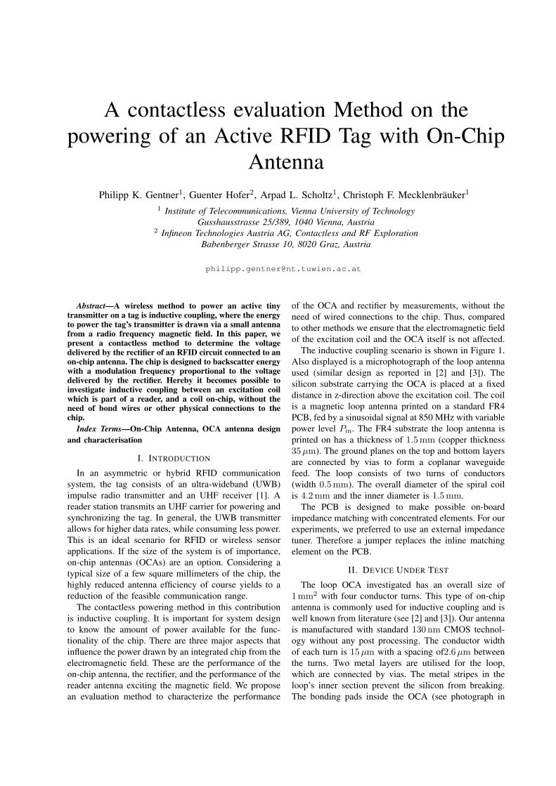
The inductive coupling scenario is shown in Figure 1.Also displayed is a microphotograph of the loop antennaused (similar design as reported in [2] and [3]). Thesilicon substrate carrying the OCA is placed at a fixeddistance in z-direction above the excitation coil. The coilis a magnetic loop antenna printed on a standard FR4PCB, fed by a sinusoidal signal at 850 MHz with variablepower level Pin. The FR4 substrate the loop antenna isprinted on has a thickness of 1.5mm (copper thickness35µm). The ground planes on the top and bottom layersare connected by vias to form a coplanar waveguidefeed. The loop consists of two turns of conductors(width 0.5mm). The overall diameter of the spiral coilis 4.2mm and the inner diameter is 1.5mm.
The PCB is designed to make possible on-boardimpedance matching with concentrated elements. For ourexperiments, we preferred to use an external impedancetuner. Therefore a jumper replaces the inline matchingelement on the PCB.
II. DEVICE UNDER TEST
The loop OCA investigated has an overall size of1mm2 with four conductor turns. This type of on-chipantenna is commonly used for inductive coupling and iswell known from literature (see [2] and [3]). Our antennais manufactured with standard 130 nm CMOS technol-ogy without any post processing. The conductor widthof each turn is 15µm with a spacing of2.6µm betweenthe turns. Two metal layers are utilised for the loop,which are connected by vias. The metal stripes in theloop’s inner section prevent the silicon from breaking.The bonding pads inside the OCA (see photograph in

Fig. 1. Inductive coupling scenario. The silicon chip with the OCA is placed in close distance in z-direction directly above the center of theexcitation coil. On the right side, a microphotograph of the chip with a 4-turn coil antenna is shown.
Fig. 2. The backscattered signal of the chip in the frequency domain.
Figure 1 are not required for the measurements presentedin this paper.
The circuit on the silicon chip features a rectifier [4],a voltage controlled oscillator [5], and a logic part. Therectifier powers the chip. The oscillator and the logicpart generate a modulated output signal that is fed tothe OCA. Figure 2 shows the corresponding measuredoutput spectrum. The peaks in the backscattered sig-nals’ spectrum are offset from the sinusoidal carrierat 850MHz by multiples of the modulation frequencyfmod. The modulation frequency fmod is proportional tothe chip voltage VDD (induced by the excitation antenna)after the rectifier.
Fig. 3. Simulated proportionality between the modulation frequencyfmod and the induced voltage VDD, delivered by the rectifier.
The proportionality between fmod and the chips’ VDD
is calculated by transient simulation of the oscillator(see Figure 3). The simulation, performed with Cadence,incorporates the parasitic effects of the substrate. Thismethod to conclude from the measured fmod to VDD,allows to determine the performance of the OCA andthe rectifier without the need of wired connections.
III. MEASUREMENTS
To show the feasibility of our method several experi-ments were carried out. The setup for all measurementsconsists of two styrofoam elements, one carrying theexcitation coil and the other carrying the device under

test. The excitation coil (see Figure 1) was matched witha tuner to the RF source. The matching process was donewithout the chip being in the excitation coil’s vicinity.The chip was fixed with a double-faced adhesive tapeon one end of the dedicated long styrofoam board. Theother end was mounted on a multi axis platform, whichcan be moved in x, y and z direction via micrometerscrews.
To get a first insight into the power transfer properties,the following initial experiment was performed. Forconstant input power Pin = +8.6 dBm at the excitationcoil and constant z-position, the chip was moved inthe x-y plane, until the measured fmod reached itsmaximum. The coordinates such obtained are used asthe origin x = y = 0. Now, the chip was moved inthe x-y plane in equidistant steps of 0.5mm. For eachof these steps the modulation frequency was measured,and used to calculate the induced voltage VDD. Thismeasurement was carried out for two different z values(0.5mm and 1.5mm). Figure 4 shows the correspondingresults. The induced voltage VDD decreases with distancein z-direction as expected. Keeping in mind that chipoperation requires a certain minimum VDD level, thearea of sufficient induced power decreases with height,as can be deduced from Figure 4 in accordance withexpectation.
Next, a distance sweep in z-direction at x = y = 0 mmwas carried out. For this range test, the styrofoam armwith the chip under test was moved from z = 0.5mm to z= 2.75mm, while the input power Pin was kept constant.The VDD values resulting from the measured fmod areshown in Figure 5. The induced voltage decreases withincreasing distance from the excitation coil, from 1.66Vat z = 0.5mm to 0.47V at z = 2.75mm.
Finally, the chip was brought into contact with theexcitation coil (x = y = z = 0mm), and the input powerPin of the excitation coil was varied from −6.4 dBmto 5.6 dBm (see Figure 6). This was done to see howmuch power can be transferred into the chip in anideal scenario. We observe that the induced voltage VDD
increases from 0.5V to 2.13V.
IV. CONCLUSIONS
In this paper we presented a contactless method todetermine the voltage induced by an excitation coil to anOCA. The modulation frequency of the signal backscat-tered from the tag is proportional to the induced voltageVDD after the rectifier. This method was verified bymeasurements on an RFID chip prototype with an OCA.The tags operational area at constant heights above theexcitation coil, as well as the behavior with increasingdistance was successfully measured. Also, the voltageprovided by the rectifier in an ideal scenario, with zerodistance to the excitation coil has been measured. This
Fig. 5. Range test in z-direction with Pin = 8.6 dBm at max VDD
position.
Fig. 6. Input power sweep at z = 0 mm.
information will help in optimally designing inductivelypowered RFID chips with on-chip antennas.
ACKNOWLEDGEMENTS
This work was performed as part of the project‘Smart Data Grain’ which is embedded into the pro-gram ‘Forschung, Innovation, Technologie - Informa-tionstechnologie’ (FIT-IT) of the ‘Bundesministeriumfur Verkehr, Innovation und Technologie’ (BMVIT).This program is funded by the ‘OsterreichischeForschungsforderungsgesellschaft’ (FFG). This work ispartly supported by the Christian Doppler Laboratoryfor Wireless Technologies for Sustainable Mobility. Theauthors would like to thank the members for supportduring manufacturing and measurements.
REFERENCES
[1] L.-R. Zheng, M. B. Nejad, Z. Zou, D. S. Mendoza, Z. Zhang, andH. Tenhunen, “Future RFID and Wireless Sensors for UbiquitousIntelligence,” in Proc. NORCHIP, 2008, pp. 142–149.

Fig. 4. Measured VDD for two different heights above the excitation coil. zleft = 0.5 mm and zright = 1.5 mm.
[2] J. Xi, N. Yan, W. Che, X. Wang, H. Jian, and H. Min, “On-chipantenna design for UHF RFID,” Electronics Letters, vol. 45, no. 1,pp. 14–16, 2009.
[3] L. Guo, A. Popov, H. Li, Y. Wang, V. Bliznetsov, G. Lo,N. Balasubramanian, and D. Kwong, “A small OCA on a 1 x0.5mm2 2.45GHz RFID Tag- Design and Integration Based on aCMOS-Compatible Manufacturing Technology,” Electron DeviceLetters, IEEE, vol. 27, no. 2, pp. 96–98, 2006. [Online]. Available:http://ieeexplore.ieee.org/xpls/abs all.jsp?arnumber=1580593
[4] H. Reinisch, S. Gruber, M. Wiessflecker, H. Unterassinger,G. Hofer, W. Pribyl, and G. Holweg, “An electro-magnetic energyharvester with 190nW idle mode power consumption for wirelesssensor nodes,” in Proc. ESSCIRC, 2010, pp. 234–237.
[5] C. Klapf, A. Missoni, W. Pribyl, G. Holweg, and G. Hofer, “Anal-yses and design of low power clock generators for RFID TAGs,” inProc. Ph.D. Research in Microelectronics and Electronics PRIME2008, 2008, pp. 181–184.