Embed Size (px)
Citation preview

SCHOOL OF MATERIALS, THE UNIVERSITY OF MANCHESTER
A Comparison of nanowire production
methodologies Copper electrodeposition into etched ion-track polycarbonate and porous anodised aluminium
oxide templates
Matthew Webb
2013
Advanced Metallic Systems CDT
The University of Manchester

1
Abstract
Metal wires have been found to have increasing yield strengths with decreasing diameters
in the sub-micron regime. Previous work in Manchester has shown that there is a universal
scaling law for FCC metals. A lack of reliable method for the production of nanowires below
200nm in diameter has resulted in there being few studies of wires below this size.
Electrodeposition into a template is a promising method for producing wires of sufficiently
low diameter. Two templates were compared: commercially available etched ion-track
polycarbonate filters (EMD Millipore Corporation, Billerica, MA, USA), and porous anodised
aluminium oxide films grown by a two-stage anodising process.
Electrodeposition into the polycarbonate templates was successful, with a pore filling rate
of 90% achieved. However the templates were found to have a larger than specified pore
diameter and a large variation in the size of the pores (970nm ± 245nm for templates specified
as 800nm). This was due to overlapping pores formed during the random radiation production
method. Pore angles were also found to be non-perpendicular to the template surface. Thus, the
templates are not suitable for growing nanowires for mechanical testing. The alumina pores were
found to have a more suitable pore size distribution and pore angle; however issues with preparing
the templates for electrodeposition caused unsatisfactory deposition to occur.

2
Acknowledgements
Many thanks to my supervisor Brian Derby for invaluable guidance and advice given
throughout this project. Thanks also to Rui Dou for experimental help and Joseph Ward for
his enthusiasm during his time on the project. Thanks to Michael Faulkner for his essential
help during SEM sessions.
A huge thank you to Claire Hinchliffe and Brad Wynne of the Advanced Metallic Systems
CDT for being supportive and understanding throughout my time at the CDT. Thanks also to
my course mates on the CDT for making my time there thoroughly enjoyable (and providing
a roof over my head!).
Finally, a massive thanks to my family, friends, band mates and other assorted loved ones
for their continuing support. I really appreciate it.

3
Contents
1. Introduction .................................................................................................................................... 5
1.1. Aims and objectives ................................................................................................................ 7
2. Manufacture of nanowires ............................................................................................................. 8
2.1. FIB milling ................................................................................................................................ 8
2.1.1. Limitations and Drawbacks of FIB milling nanopillars .................................................. 11
2.2. Selective Etching of Eutectic Microstructures ...................................................................... 14
2.3. Electrodeposition into template ........................................................................................... 16
2.3.1. AAO templates .............................................................................................................. 16
2.3.2. Ion track templates ...................................................................................................... 22
2.4. Summary of production methods ......................................................................................... 28
3. AAO Film growth ........................................................................................................................... 30
3.1. Barrier Films .......................................................................................................................... 30
3.2. Porous Films .......................................................................................................................... 31
3.3. Pore regularity ...................................................................................................................... 34
3.4. Pore size ................................................................................................................................ 35
4. Deformation mechanisms and mechanical testing of nanowires ................................................ 36
4.1. Deformation mechanisms in sub-micron diameter nanowires ............................................ 36
4.1.1. Storage of geometrically necessary dislocations .............................................................. 37
4.1.2. Dislocation starvation and dislocation nucleation ............................................................ 38
4.2. Mechanical testing of nanowires .......................................................................................... 39
4.2.1. Testing in bending ......................................................................................................... 39
4.2.2. Nanoindentation ........................................................................................................... 42
5. Experimental methods .................................................................................................................. 48
5.1. Porous anodic aluminium oxide (AAO) templates ................................................................ 48
5.2. Etched ion track polycarbonate templates ........................................................................... 51
5.3. Electrodeposition of copper into templates ......................................................................... 51
6. Results and discussion .................................................................................................................. 52
6.1. Polycarbonate membrane pore analysis .............................................................................. 53
6.1.1. 800nm template analysis .............................................................................................. 53
6.1.2. 400nm template analysis .............................................................................................. 59

4
6.1.3. 220nm template analysis .............................................................................................. 60
6.1.4. 100nm template analysis .............................................................................................. 62
6.1.5. Pore angle ..................................................................................................................... 62
6.1.6. Polycarbonate damage susceptibility ........................................................................... 63
6.1.7. Summary of etched ion track polycarbonate template analysis .................................. 66
6.2. Electrodeposition into polycarbonate membrane ................................................................ 67
6.2.1. Sample 1 ........................................................................................................................ 67
6.2.2. Sample 2 ........................................................................................................................ 69
6.2.3. A note on current density-time plots ............................................................................ 72
6.2.4. Sample 3 ........................................................................................................................ 72
6.2.5. Sample 4 ........................................................................................................................ 73
6.2.6. Summary of electrodeposition into polycarbonate templates ..................................... 76
6.3. Aluminium Oxide template growth ...................................................................................... 76
6.3.1. First stage anodisation .................................................................................................. 76
6.3.2. Ridges formed on aluminium ........................................................................................ 77
6.3.3. Second stage anodisation ............................................................................................. 78
6.4. Electrodeposition into AAO templates ................................................................................. 81
6.4.1. Sample 1 ........................................................................................................................ 81
6.4.2. Sample 2 ........................................................................................................................ 84
6.4.3. Sample 3 ........................................................................................................................ 87
6.4.4. Summary of electrodeposition into porous aluminium oxide templates ..................... 89
6.5. Etched ion track polycarbonate templates vs. AAO templates ............................................ 90
7. Conclusion ..................................................................................................................................... 92
8. Future works ................................................................................................................................. 94
References ............................................................................................................................................ 97

5
1. Introduction
Size effects, in terms of dimensions of internal features, are well known to change a
material’s properties. An example of this is the Hall-Petch relationship in metals, which
states that the metal’s yield strength is inversely proportional to the square root of the
average grain diameter [1,2]. This relationship holds for grain diameters ranging from
millimetres down to tens of nanometres [3]. Sample size effects have been less thoroughly
investigated however, as classical mechanics traditionally states that a material’s properties
are independent of sample size.
Sample size effects have been observed, however, as early as 1951, where micrometre scale
metallic whiskers were shown to have an increasing yield strength in tensile testing with
decreased whisker diameter [4]. This has led to studies of the mechanical properties of
nanowires with sub-micron diameters.
Prior works have shown that this ‘smaller is stronger’ tenet is apparent in metal nanowires.
In the sub-micron regime a nanowire’s yield strength increases with reducing diameter [5,6].
A previous project in Manchester has proposed a relationship between the strength, ,
normalised by shear modulus, , and the wire diameter, , normalised by Burgers vector, ,
for face-centred cubic (FCC) nanowires (shown in Equation 1 and Figure 1) [7].
(
)
Equation 1

6
Figure 1: Plot of Normalised shear stress against Normalised pillar diameter for a variety of FCC
nanowires showing linear fit [7].
This paper only includes one result with pillars of diameter less than 180nm. A contributing
factor to this is a lack of reliable methods for producing nanowires below approximately
200nm in diameter, with FIB milled pillars (with diameters greater than ~200nm) more
commonly investigated.
Above this diameter, both BCC and FCC nanowires have been produced via methods
including focussed ion beam (FIB) milling and by etching away the matrix of a eutectic
composite [5,8]. FCC metals have been investigated below this diameter using an
electrodeposition into anodised aluminium oxide (AAO) templates method, based on the
process by Masuda and Fukuda and developed by Dou and Derby [9][10][11]. More research

7
on nanowires below that achievable via FIB milling is required to fully understand the
strengthening processed occurring.
1.1. Aims and objectives
The main aim of this project was to show that it is possible to produce copper nanowires via
electrodeposition in two different types of template: porous aluminium oxide and pre-
manufactured track-etched polycarbonate (EMD Millipore Corporation, Billerica, MA, USA).
A comparison of the two methods was also carried out. The steps taken to achieve this aim
were as follows:
A literature review was conducted on the various methods used to produce
nanowires, as well as the deformation mechanisms in the sub-micron regime and
mechanical testing mechanisms.
Training at techniques such as electropolishing, anodising and electrodeposition
required for the production of nanowires.
Training in analytical and imaging techniques including scanning electron microscopy
in order to view the templates and nanowires.
Literature review
Following is a review and summary of the different methods used to produce metal
nanowires, including: FIB milling, selective etching of a eutectic matrix and electrodeposition
into a variety of different templates. Different strengthening mechanisms that explain the
size dependent increase in strength have been suggested and these are discussed and
reviewed, as well as a variety of different mechanical testing methods used to characterize

8
the materials. A section on the growth of porous aluminium oxide is also included due to its
relevance to the project as a template.
2. Manufacture of nanowires
Research into metal nanowires has been ongoing for a quarter of a century for a variety of
purposes, including in magnetic, electronic and optoelectronic devices [12]. Nanowires have
been produced using a variety of methods, each with benefits and limitations: size and
otherwise. The following section details the various methods of producing nanowires of
various metals reported in literature. Some of the nanowires reported were produced in
order to perform strength and deformation testing while some were produced for other
investigations.
2.1. FIB milling
FIB (Focused Ion Beam) milling of nanopillars was developed by Uchic et al. in 2002 and
reported in literature in 2004 [5,13]. A FIB machine can be used for either imaging or
sputtering/milling. For imaging applications a low beam current is used, whereas a high
beam current is used for sputtering and milling. For milling applications the ions in the beam
(usually but not exclusively Gallium+ ions) knock atoms out of their lattice sites. If sufficient
energy is transferred to the target atom it can create a collision cascade where the displaced
atom interacts with further atoms in the lattice [14]. The effects of this are discussed later in
this section.

9
Figure 2: FIB image of FIB milled nanopillars with diameters of a) 860nm and b) 300nm [6].
In the Uchic et al. study nanopillars ranging from 500nm to 4000nm were machined from a
bulk sample crystal [5]. The location in the bulk was selected within a single grain so as to
produce single crystal nanopillars. Nickel was first used because the mechanical behavior of
bulk nickel is well known. An intermetallic alloy, Ni3-Al-Ta was also used to create
nanopillars as this has shown distinctly different flow mechanisms and so comparisons of
compression data could be made with the pure Nickel. The operating parameters of the FIB
machine, such as beam current, were not detailed. The diameters of the nanopillars
produced ranged from 4000nm to 500nm with aspect ratios of between 2:1 and 4:1 [5].
These aspect ratios were much lower than that of metal whiskers reported by Brenner in
1956 which had aspect ratios of around 1000:1 [4]. Mechanical testing of the nanopillars
was performed with a nanoindentor equipped with a flat-punch tip [5]. This is method is
discussed in Section 4.2. Mechanical testing.

10
Figure 3: Schematic diagram of a FIB machine[14].
Uchic et al.’s method was developed by Greer et al. in 2005 and applied to gold for the first
time, and the minimum nanowire diameter was reduced to 400nm [6,15]. Gold nanopillars
with diameters of 400nm and 7450nm were produced via a FIB milling method with aspect
ratios of approximately 3:1. A single crystal <0 0 1> oriented gold disk was used as a
precursor. A gallium ion beam with beam current of 3000pA was used to machine a circular
crater with a 4000nm diameter pillar remaining in the center (see Figure 2). This pillar was
then machined into a pillar of the required diameter and aspect ratio by using finer beam
currents and by adjusting the tilt angle of the sample [6,15].
Further works on FIB milling of nanopillars have been carried out using a similar method to
that detailed above on a variety of materials, including gold, nickel, molybdenum and
niobium [5,6,15–26]. A summary of prior studies is shown in Table 1.

11
Author Date Material Crystal structure Diameter
Uchic et al. [5] 2004 Nickel Ni3-Al-Ta
FCC 500nm – 4000nm
Greer & Nix [15] 2005 Gold FCC 400nm – 7450nm
Greer et al. [6] 2005 Gold FCC 400nm – 7450nm
Volkert & Lilleodden [16] 2006 Gold FCC 180nm – 8000nm
Greer & Nix. [25] 2006 Gold BCC 290nm – 7450nm
Kim & Greer. [23] 2008 Molybdenum BCC 200nm – 900nm
Brinckmann et al. [26] 2008 Gold Molybdenum
BCC 250nm – 946nm 205nm+
Shan et al. [17] 2008 Nickel FCC 150nm – 400nm
Frick et al. [27] 2008 Nickel FCC 165nm – 4500nm
Schneider et al. [19] 2009 Molybdenum Niobium
BCC
300nm – 3000nm
Schneider et al. [18] 2009 Molybdenum BCC 200nm – 5000nm
Kim & Greer. [22] 2009 Gold Molybdenum
FCC BCC
250nm – 1000nm
Kim et al. [21] 2009 Niobium BCC 200nm – 900nm
Kim et al. [20] 2010 Tungsten Molybdenum Tantalum Niobium
BCC
Han et al. [24] 2010 Vanadium BCC 183nm – 2790nm
Table 1: Summary of FIB milled nanowire studies.
2.1.1. Limitations and Drawbacks of FIB milling nanopillars
FIB milling of nanopillars is advantageous in that it can be applied to a wide range of sample
materials and it is relatively easy to produce a range of diameters of nanowire specimens to
study any size effect [16]. The method does however have a number of drawbacks, notably
contamination by the Ga ions in the beam implanting into the sample material and
consequent surface damage caused by irradiation [28]. Kiener et al. investigated a range of
aspects of the FIB process that could have an impact on mechanical properties. An
amorphous layer containing gallium ions of between 2nm and 50nm thickness, depending
on the beam current used, is formed on the surface of the sample. Gallium ions can also
penetrate and implant in the surface of the sample up 40 – 50nm, i.e. the same depth as the
amorphous layer. The mean surface roughness of a FIB milled sample was shown to be

12
between 10.7nm and 16.4nm, an increase from a roughness of 10.6nm pre-milling. This
increase of surface roughness was independent of milling conditions such as incident angle
and beam current. FIB milling can also introduce defects into the sample material such as
point defects, dislocations and precipitates. These various effects were shown to have an
influence on the mechanical properties of the sample, with yield stress increases from
several MPa and up to GPa depending on the type of hardening occurring [29].
Figure 4: Schematic diagram showing possible changes caused to a nanowire by FIB milling. ta shows the amorphous layer at the surface of sample while td shows an area
with precipitates and dislocations [29].
A further study into the dislocations introduced by the FIB milling process was undertaken
by Bei et al. in 2007 [30]. This study suggests that the dislocations added by the FIB milling

13
decrease the strength of the nanopillars and that a FIB machined sample will not reach the
theoretical strength of the material whereas non-FIB machined samples have been shown
to achieve this [8,30].
In contrast to this a study by Shan et al. in 2008 argues that the FIB milling production
method actually causes the increase in strength demonstrated [17]. Two types of dislocation
are present in a FIB milled sample: loop-like dislocations that are small in size and larger line
defects that can extend through the entire pillar. It was suggested that the line defects were
pre-existing dislocations present in the bulk crystal pre-milling and that the small loop
dislocations were introduced by the FIB milling process. The study goes on to show that the
dislocations are removed via a process of mechanical annealing in the early stages of
deformation, and this dislocation-free state is suggested to be the cause of the high
mechanical strengths shown in FIB nanopillars [17]. This is also discussed in the Bei et al.
paper, which introduces the possibility that the FIB-damaged layer on the surface of the
sample has an increased hardness in comparison to the undamaged sample. As the samples
are reduced in diameter, the proportion of harder damaged material increases, increasing
the strength of the sample [8].
A further disadvantage of FIB milled pillars is the noticeable vertical taper in the pillars (see
Figure 5). This taper is more severe as pillars of lower diameter are produced [31]. Zhang et
al. reported that taper in the pillar results in a non-uniform strain distribution in the pillar
during mechanical testing resulting in an increased measured elastic modulus as well as
taper induced hardening [32].

14
Figure 5: SEM images of Au nanopillars produced by electrodeposition [(a) to (h)], and FIB milling (i), showing noticeable taper in the FIB sample.
FIB milling has been shown to have an effect on the mechanical properties on nanowires, by
either strengthening or weakening mechanisms or a combination of both. The effects
discussed in this section intensify as the sample size is reduced, and this is perhaps the
reason that FIB nanopillars have not been produced with diameters of below 150nm. There
is therefore a need to look into alternate methods for the production of nano-scale samples.
2.2. Selective etching of eutectic microstructures
A novel method for producing nano-scale pillars for mechanical testing while avoiding the
issues introduced by the FIB milling process was developed by Bei et al. in 2007 [8]. Here,
Bei et al. furthered a method of growing a Nickel-Aluminium-Molybdenum matrix by

15
directional solidification developed by the same group in 2005 [33]. An Ni-45.5Al-9Mo (at%)
alloy was melted and drop cast into a copper mold. An optical floating zone furnace was
used to directionally solidify the ingots. These rods were used as the feed material and
directionally solidified rods were used as seed material and were heated with a xenon arc
lamp. A homogeneous molten zone was ensured by rotating the seed and feed rods in
opposing directions. This process results in a rod-like eutectic microstructure with a NiAl
matrix and Molybdenum fibers as shown in Figure 6 [33]. In the 2007 Bei et al. study, the
molybdenum fibers were exposed by preferentially etching away the matrix. The diameter
of the exposed nanopillars was taken to be square root of the cross-sectional area of the
pillar due to their square cross-sections. Bei et al. produced nanopillars ranging from 360nm
to 1000nm using this method [8].
Figure 6: SEM images of NiAl-Mo eutectic alloy showing (a) transverse view, (b) longitudinal view and (c) high magnification transverse view, where the NiAl matrix has been preferentially etched [33].

16
The preferential etching of a directionally solidified eutectic method of producing
nanopillars has advantages over the FIB method. However, there have been limited studies
using this method and the minimum diameter of nanopillars produced is 360nm. Whilst
eliminating the structural effect of the FIB process, this method does not reduce the lower
limit to diameters of nanowires. The method is also only viable with materials showing an
appropriate fibrous eutectic microstructure. Therefore a different method of nanowire
production is required to investigate the properties of nanowires of different metals below
the 150nm lower limit of FIB.
2.3. Electrodeposition into templates
A promising method of producing nanowires with sub-150nm diameters is by
electrodeposition into a porous template. This method is limited only by the size of pores
present in a template film. Templates, including lab-produced and commercially available
ion-track etched polymers and lab-produced porous aluminium oxide templates, are
discussed in this section.
2.3.1. AAO templates
Porous anodised aluminium oxide (AAO) templates have been shown as viable for the
electrodeposition of nanowires using a variety of materials. Aluminium oxide pores have
been shown to be self-organizing during anodizing under appropriate conditions [34,35].
Using an appropriate electrolyte a variety of different metals can be electrodeposited into
the pores. Further details on the growth of AAO templates and methods of increasing pore
regularity are included in section 3. AAO Film growth.

17
A DC electrodeposition method was used by Dou & Derby in 2008 to produce gold
nanowires using AAO templates. A schematic diagram is show in Figure 7 and the following
labeled steps correspond to that diagram. An AAO template was produced using the
Masuda and Fukuda two-stage anodizing method (discussed in section 3.3) [9–11]. 99.999%
pure aluminium was first electropolished in a perchloric acid-ethanol mixture. One surface
of this substrate was anodised at 40V for 12 hours. To improve pore regularity the oxide film
formed was removed by etching in a 0.1M chromic acid and 0.1M phosphoric acid mixture
(a). The substrate was then anodised a second time for 2 hours (b). 0.1M phosphoric acid
was then used to etch the template and produce different pore diameters. PMMA was
coated onto the surface of the film (c) and the aluminium substrate was removed by etching
in 0.1M copper chloride solution (d). The oxide barrier layer was removed using copper
chloride solution (e). A gold layer was sputtered onto the template to act as a conductive
substrate (f). The PMMA layer was dissolved (g) and Gold nanowires were electrodeposited
into the template using an 0.02M KAu(CN)2 and 0.25M Na2CO3 electrolyte of pH13 (h). The
gold coated template was used as the working electrode and a platinum mesh was used as a
counter electrode with a voltage of -1.2V DC at an Ag/AgCl reference electrode. A 3M NaOH
solution was used to etch away the top of the AAO template, leaving the gold nanowires
exposed (i). Each nanowire was reported to be a single crystal with a random
crystallographic orientation resulting in no overall texture. Gold nanowires with diameters
30nm to 80nm were produced via this method. Different pore diameters were produced by
chemically etching the 30nm pores in 0.1M phosphoric acid for up to 60 minutes to thin the
cell walls and thus widen the pores to 55nm (30 minute etch) and 80nm (60 minute etch)
[11].

18
Figure 7: Schematic diagram showing method of producing gold nanowires by Dou [36].
Dou also produced nickel and copper nanowires using the same method [36]. Nickel
nanowires were deposited using an aqueous solution of 0.5M NiSO4∙6H2O, 0.1M NiCl2∙6H2O
and 0.2M H3BO3. Aluminium oxide has been shown to dissolve at a pH of less 4.2 and so
35M Na2SO4 was added to adjust the pH value from pH4 to pH4.8 and 0.01M C7H4NNaO3S
was added to increase adhesion. This study reports a pore filling ratio of 90%, however the
electrodeposition was inhomogeneous and pores were filled at different rates. This causes
some pores to overflow with nickel and form balls on the surface of the template. A precise

19
ion beam polish system (PIPS) was used to create a smooth surface with nanowires of
uniform height [36].
Figure 8: SEM image of gold nanowires [36].
Gelves et al. reported in 2006 that the DC electrodeposition methods can be difficult due to
the need to remove the oxide barrier layer leaving fragile AAO films [37]. Gelves suggested
an AC electrodeposition method wherein the AAO barrier layer can be sufficiently thinned
to allow electrodeposition without the need to remove the aluminium substrate and the
oxide barrier layer formed between the aluminium and the pores. A two-step anodizing
process was performed in 0.3M sulfuric acid at 25V for 2 hours for the first stage and 4, 6 or
8 hours for the second stage. After completion of the second anodizing step the voltage was
gradually decreased from 25V to 9V over 16 minutes and held for 5 minutes to reduce the
thickness of the barrier layer (this process is known as current limitation. Barrier layer

20
thickness is proportional to anodizing voltage (see Section 3 for more details). Copper was
electrodeposited into the pores from a 0.5M CuSO4 and 0.285M H3BO3 aqueous solution
using a 200Hz sine wave at 10Vrms for 10-15 minutes. The aluminium substrate was used as
one electrode and a copper plate as the counter electrode. The proportion of pores filled
using this method is between 20% and 60% with the nanowires produced having a diameter
of 20nm. The nanowires were liberated and dispersed for SEM imaging by dissolving the
substrate and no mechanical testing was carried out [37].
An AC electrodeposition method was also reported by Borissov et al in 2009 [38]. Here the
author used a two stage anodizing process as mentioned above. After the second anodizing
stage the sample was etched in 2M sulfuric acid to reduce the barrier layer thickness and
widen the pore diameter. Iron was deposited into the pores using an alternating current at
300Hz and 35Vac, in an electrolyte containing 120g/L FeSO47H2O, 45g/L boric acid and 0.5
g/L ascorbic acid. Nanowires grown using this method had a mean pore diameter of 50nm ±
2nm. The proportion of pores filled was reported to be almost 100%, a feat attributed to the
thinning process of the barrier layer [38].
Figure 9: Schematic diagram showing advantages of AC electrodeposition over DC [37].

21
A third method of pulsed electrodeposition (PED) has also been investigated. The process
was first reported by Nielsch et al. in 2000 and is similar to that of the AC electrodeposition
process [39]. A porous AAO template is produced using a two-step method, and the
aluminium oxide barrier layer is thinned by chemical etching or by current limitation [40].
Metal is electrodeposited into the pores using a millisecond voltage pulse followed by a gap
of around 1 second (see Figure 10). The negative pulse causes electrodeposition of the
metal in the pore bottom while the positive pulse discharges any capacitance in the barrier
layer as well as repairing any discontinuities in the oxide layer [40]. PED offers more control
over operation parameters than AC deposition such as ion concentration in the pores, as the
time delay allows for ion diffusion from the pore bottom to the pore opening [39]. Nielsch
reported a pore diameter of 45-55nm with a pore filling rate of almost 100%. This filling rate
is highly dependent on the amount of thinning of the barrier layer, and fewer pores are
filled in areas where the barrier layer is thicker [39].
Figure 10: Pulsed electrodeposition method signal plot [40].

22
Electrodeposition into a porous alumina template can be performed using DC, AC or PED
methods. Both AC and PED methods have less production stages and as such are simpler.
Both however depend on the barrier layer being thin enough to allow ion transfer. DC
electrodeposition requires more production stages, including the removal of the original
aluminium substrate. This necessitates working with extremely delicate freestanding porous
alumina film. However, once the template is prepared for electrodeposition, the process is
more straightforward and deposition can be performed in the pores without the intervening
alumina barrier layer.
2.3.2. Ion track templates
An alternative to using porous AAO templates for the electrodeposition of nanowires is to
use etched ion track templates. These templates can be produced by chemically etching a
sample which has been exposed to ionizing radiation. This process was first demonstrated
by Possin in 1970 who produced tin, indium and zinc wires with diameters as small as 40nm
[41]. Radiation damage tracks in mica were etched in strong acid via a process
developed by Fleischer and Price [42]. Possin chose Mica as a template material due to its
large relative etching rates along the track axis to transverse to the axis. This results in
almost uniform pores throughout their 12μm length. The pores were filled by an
electroplating process and the produced wires have an almost uniform cross section with
diameters ranging from 40nm to 100nm [41].
A similar template method was used by Molares et al. to produce copper wires in 2001 [43].
Here the authors used polycarbonate foils between 30 and 40μm as a template. The foils
were irradiated with Au197 and Pb208 ions with sufficient energy per nucleon (11.4MeV) that
the penetration range was larger than the thickness of the foils and that the stopping power

23
of the ions (dE/dx) was large enough to result in homogeneous etching of the pores. The
foils were then chemically etched with 6M NaOH solution at 50°C, with 10% methanol as
well as 1% surfactant. Different pore diameters of between 30nm and 200nm were created
by adjusting etching time. A 100nm gold layer was sputtered onto the membrane to serve
as a cathode for electrodeposition. A copper electrode was used as an anode in a two-
electrode electrochemical cell, with the sputtered gold substrate used as the cathode. The
anode used was cone shaped in order to ensure homogeneous deposition throughout the
sample. A high concentration copper sulfate pentahydrate solution (238g/L) was used as an
electrolyte to ensure a sufficient amount of copper ions were available for
electrodeposition. The electrical conductivity of the solution was increased by adding 21g/L
sulphuric acid, which also has the effect of lowering the cathode overvoltage. The wires
produced were shown to be either single crystals, or poly crystalline (depending on
electrodeposition conditions) by X-ray diffraction and TEM analysis. The authors conclude by
stating that polycarbonate ion track films are suitable for the production of nanowires up to
30μm in length and as low as 30nm in diameter.
Figure 11: SEM image of single (a) and poly (b) crystalline copper wires in pores as well as overgrown caps on the surface of a polycarbonate template [43].

24
A second paper published by Molares in 2001 provides a more in depth investigation into
the electrodeposition conditions that produce single or polycrystalline wires [44]. Single
crystals were produced when existing nuclei growth dominated the nucleation and
formation of new grains. Parameters thought to affect this, and thus investigated, were
current density (controlled by varying the electrodeposition cell voltage), temperature and
the type of electrolyte used. When a commercial electrolytic copper bath is used as the
electrolyte and a constant current density applied, increasing the temperature caused the
wires grown to be single crystals. The transition temperature between poly and single
crystals occurs at 60°C. Below this temperature, additions in the solution, including
brightening agents, are absorbs at the cathode’s surface, which increases the cathode
overvoltage and thus increases the electrode polarization. Increasing the temperature
decreases this cathode overvoltage, as well as increases both surface diffusion and efficient
transport of ions towards the electrode. A combination of these effects is attributed to
encourage growth of existing nuclei, and thus create single crystal wires. In a simple salt
electrolyte (the same 238g/L copper sulfate pentahydrate solution as used in the previous
paper), decreasing the current density was shown to favour have the same effect as
increasing the temperature in the previous setup and single crystal nanowires were grown
for current densities below 35mA/cm2 at both 50°C and 60°C.
The two Molares papers reveal four different regimes during electrodeposition (see Figure
12). A peak in current at the beginning of electrodeposition is attributed to the charge of the
double layer and the creation of the diffusion layer. A constant (albeit slightly decreasing)
current is then shown during growth of the nanowires in the pores. Once the pores fill, caps
begin forming on the film surface, increasing the electrodeposition area and thus increasing

25
current flow. Finally the caps combine to become a layer and current flow becomes
constant again (at a higher rate than during nanowire growth due to the increased area)
[43]. Increasing the current density (by increasing the voltage) causes the copper to fill the
pores more rapidly as expected. Current density was also shown to increase lineally with
applied voltage. This knowledge of current flow is important during electrodeposition as in
order to observe the nanowire grown it is preferable to stop the process at the end of the
2nd phase before caps are grown on the surface of the film. Performing the
electrodeposition at a lower voltage and increasing the time before caps form would offer
more control.
Figure 12: Schematic current time diagram (left) and current time curves for different applied voltages (right) during copper deposition into polycarbonate pores. [43,44]
Enculescu et al. used a similar method to grow copper nanowires in a polycarbonate ion
track template, however unlike Molares et al. who grew a ‘forest’ of wires, single nanowires
were produced [45]. Enculescu argued that single nanowires can be used to more accurately
measure electric properties. A 30μm polycarbonate film was irradiated by a single heavy ion
with kinetic energy of greater than 1GeV. A gold layer was sputtered onto the back of the
foil as support and for use as a cathode and the ion track damage trail was etched in a

26
solution containing sodium hydroxide and methanol. The composition of the etching
solution was show to have an effect on the pore shape: as it adjusts the etching velocity
along the track and the etching rate of the bulk at a different rate. In an etching solution
with no methanol pore diameter was measured to be 160nm at the pore opening and 40nm
close to the tip and the pore was described as almost cylindrical. Adding methanol to the
etching solution increases the etching rate across the bulk, , compared to the etching
rate along the track, , and thus increases the pore angle (see Equation 2). This was
thought to be an effect related to the rate of diffusion of the etchant in the pore.
( ) (
) for
Where is the pore radius at a distance along the track, is the etching time.
Equation 2
This is an important result when designing an experimental setup for creating nanowires by
a template and electrodeposition method as it shows that the wires grown adapt the same
form as the pores in the template.
Unlike the regularly ordered templates produced by a two-stage anodizing process on
aluminium, the ion track templates discussed above have either randomly spaced pores
(both Molares et al. papers) or produce single pillars (Enculescu et al.). Burek and Greer
claim that this is primarily due to limited control of pore size and placement in conventional
methods [31]. Here the authors propose an electron beam lithographic method that allows
full control over pore size and placement. This allows pores to be produced in sizes ranging
from 750nm to 25nm without the taper associated with etching of heavy ion track methods.
A 100nm gold layer is deposited onto a silicon substrate with a 20nm titanium layer

27
adhesion layer between. The gold here acts as a cathode during electrodeposition as in
other electrodeposition methods. A PMMA layer was spin coated onto the substrate at a
thickness closely matching the height of the nanopillar required and baked to set. An
electron beam lithography system was used to expose the PMMA in a computer generated
pattern. Precise isolation of nanopillars was possible and pillars were spaced up to 50μm
apart. The PMMA was developed immediately after exposure in a solution of
methylisobutylketone and isopropyl alcohol for 60s. This creates a template with attached
cathode layer akin to similar electrodeposition methods discussed in this section.
Figure 13: (a) SEM image of regularly ordered array, with both tension and compression samples, (b) to (i) FIB images of tension (with caps) and compression nanopillars.
Burek and Greer proceed to grow both gold and copper nanopillars. Gold was deposited in a
commercially available [Au(SO3)2]2- plating bath, and copper was deposited using a 125g/L
copper sulphate pentahydrate and 50g/L sulphuric acid solution. Both Galvanostatic (DC)
and reverse pulse (AC) conditions were used for electrodeposition. Deposition was stopped
when the pillars filled the pores for compression samples, and caps were allowed to form on
the surface of the template for to provide grip points for tension samples (see Figure 13).

28
Finally the PMMA template was removed in a bath of acetone. The gold nanopillars grown
were limited to nanocrystalline microstructure, with only small changes to grain size
possible. This was the case for both AC and DC deposition. This was attributed to the
electrolyte, specifically the instability of the gold sulfite salt in solution. For copper
deposition, DC current densities of below 20mA/cm2 yields single crystal pillars. This is a
lower value than the 35mA/cm2 reported by Molares et al. [44]. Deposition below
10mA/cm2 was not possible due to current being used by side reactions. AC deposition was
found to increase the percentage of single crystal pillars grown. It was found however, that
AC deposition can have effects on future mechanical testing by introducing voids and by
creating inhomogeneous pillars.
2.4. Summary of production methods
FIB milling has been used to produce nanopillars ranging from 150nm to 8000nm and in a
variety of different materials. Pillar size and aspect ratio can be selected and created with
minimal manufacturing limits. However, FIB milled pillars have a number of disadvantages.
Firstly, radiation effects from the ion beam can cause an amorphous layer up to 50nm on
the surface of the pillars, increase the surface roughness of the pillar, as well as introduce
point defects, precipitates and dislocations into the pillar. These can all have an effect on
the mechanical properties, with strengthening mechanisms, weakening mechanisms, or a
combination of the two. These effects are increased as pillar diameter is decreased,
imposing a lower limit on pillar diameter produced. FIB milled pillars also have a noticeable
vertical taper which causes non-uniform strain gradients during mechanical testing further
effecting mechanical properties.

29
Etching away the matrix of a directionally solidified eutectic results in nanopillars without
many of the disadvantages of FIB milled pillars. There is none of the radiation damage
effects associated with FIB milling and pillars are taper free. However, the method has only
been used to produce molybdenum pillars and selection of pillar diameter is limited. The
minimum diameter produced via this method is 360nm.
A final method of producing nanowires is by electrodeposition into a template. Templates
can be made with a variety of materials, with popular options being regularly ordered
porous aluminium oxide and ion track polymer templates. Nanowires grown have the same
form as the pores in the template, and as such the shape and size of wires grown is limited
only by the shape and size of the template available. Aluminium oxide templates have been
used to grow wires from 30nm up to 450nm, and pillars grown are in a regular hexagonal
array. Disadvantages of aluminium oxide templates is the complex production method
required to remove the barrier layer oxide formed between the porous oxide and the
aluminium substrate, however an AC electrodeposition process can simplify this. Polymer
templates have been used to produce wires from 25nm to 750nm. This upper value is not a
hard limit, and is only in place due to lack of relevance of studying wires above this
diameter. The pores in the templates can be produced by either etching radiation damage
tracks caused by the bombardment of heavy ions, or by electron beam lithography.
Nanowires of a variety of different metals can subsequently be grown in the templates by
electrodeposition. Single crystal or polycrystalline pillars can be grown depending on
electrodeposition conditions. The electrodeposition into a template method produces wires
that lack the radiation damage and tapering effects of FIB milled samples, and also the
method overcomes the size limitations imposed by both the FIB milling and etching of

30
eutectic methods. Electrodeposition into a template therefore provides an ideal method for
the production of nanowires for study.
3. AAO Film growth
As this project involves the production of porous aluminium oxide templates, this section is
included to discuss the theory of oxide growth and pore regularity.
Anodic alumina films can be grown in two distinct varieties: Barrier type films, which consist
of a uniformly thick amorphous layer of alumina that are often utilised as dielectrics, and
porous films, which consist of a regular series of alumina pores formed above a thin barrier
layer and have practical uses in corrosion and wear protection, as well as providing keying
layers in adhesive bonding and base layers for paints [35,46]. These films are formed by the
electro-chemical process of anodising (anodic oxidation), where the sample is used as the
anode in a circuit as direct current is passed through an aqueous electrolyte.
3.1. Barrier Films
Barrier type films are formed in electrolytes at a near-neutral pH. Al3+ ions are produced via
oxidation of aluminium atoms in the sample, and O2- ions are derived from the electrolyte.
The applied electric field causes the solid state migration of the ions towards the cathode
and anode (sample) respectively (see Figure 14). The film is formed at both the anode-film
interface and the film-electrolyte interface, with a growth ratio theoretically proportional to
the current carried by the ions: 40% at the anode-film interface, corresponding to the O2-

31
ions, and 60% at the film-electrolyte interface, corresponding to the Al3+ ions [47].
Figure 14: Schematic diagram of ion migration in the formation of a) barrier type films, and b) porous type films [48]
3.2. Porous Films
Porous films are formed in non-neutral pH electrolytes. In 1978 Thompson et al. showed
that during anodisation a non-uniform growth rate of the anodic film occurs, with thicker
film material forming above any ridges in the surface of the sample [35]. These ridges can be
formed during an electropolishing process performed on the sample during preparation, by
etching or mechanical polishing and scratching. This results in a cellular topographical
appearance on the film identical to that of the original aluminium. These ridges develop to
form roughly hexagonal cells. Pore formation occurs within these preferred cells and
continued anodisation causes pore diameter growth in order to maintain a uniform barrier

32
layer thickness, which is dependent on the voltage applied. Once the cells reach a diameter
where they interact, a steady-state porous morphology is formed.
This description was further developed by Shimzu et al. [49]. In a non-neutral pH electrolyte,
a barrier type film can only grow at the anode-film interface as outwardly migrating Al3+ ions
are lost to the electrolyte via field-assisted dissolution as well as direct injection, rather than
forming oxide. Once a certain thickness of barrier type film is formed, increased local
stresses caused by alumina being less dense than aluminium causes cracking. This critical
thickness is proportional to the applied voltage. Stress concentration factors are higher at
any protuberances in the anode, which causes any cracks that form to typically occur at
these locations. The cracks are rapidly healed at a high current density, which leads to the
thickening of the film at these locations (see Figure 15).
33
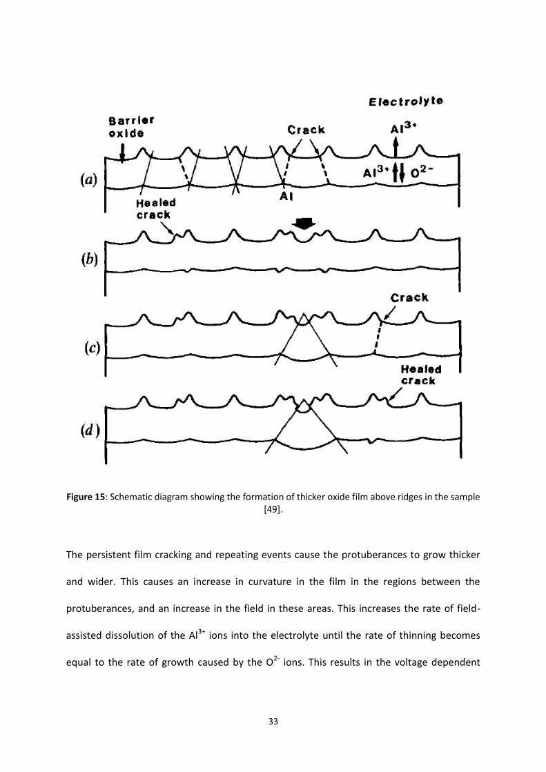
Figure 15: Schematic diagram showing the formation of thicker oxide film above ridges in the sample [49].
The persistent film cracking and repeating events cause the protuberances to grow thicker
and wider. This causes an increase in curvature in the film in the regions between the
protuberances, and an increase in the field in these areas. This increases the rate of field-
assisted dissolution of the Al3+ ions into the electrolyte until the rate of thinning becomes
equal to the rate of growth caused by the O2- ions. This results in the voltage dependent
34
uniform thickness of barrier layer observed by Thompson. At this time, barrier layer growth
is overtaken by pore growth.
Once the surface of the sample is covered by such pores, geometric constraints between the
pores force the pores to rearrange slightly into a regular hexagonal formation. This is
possibly due to a reduction in the diameters of both the cells and pores [50]. The result of
this procedure is a regularly ordered porous film above a barrier film with thickness
proportional to the applied voltage.
3.3. Pore regularity
To improve pore regularity a further process must be carried out before anodising. A
pretexturing process can be carried out where a master with hexagonal concaves is pressed
into the aluminium [51,52]. This results in a negative of the same topography on the surface
of the aluminium and serves to enhance the regularity of the ridges used for nucleation of
pores as discussed above. An alternative method for improving pore regularity is a 2-step
anodising process developed by Masuda et al. and used by Dou [10,36]. In this method a
long period anodising step is performed to produce a thick porous oxide on the surface. This
forms a hexagonal concave pattern on the surface of the aluminium as discussed in section
3.2. The oxide is then chemically etched off and the aluminium is anodised again, with the
textured ridges serving as nucleation points for the growth mechanisms discussed above.
Pore regularity is also affected by the choice of electrolyte, as well as the anodising voltage
[10][53][54].

35
3.4. Pore size
The use of different acid solutions during anodizing has an effect on the size of cell formed.
Larger cells allow larger pores to be produced as the pores must be smaller than the cell
size. Li et al. reported the pore distances (hence cell sizes) of three different acids: Sulfuric,
oxalic and phosphoric [12]. Each acid has an optimal anodizing voltage to produce regularly
ordered pores. Sulfuric acid produces 60nm cells at 25V; Oxalic acid produces 95nm cells at
40V; Sulfuric acid produces 420nm cells at 160V. Pore distance was found to increase
linearly with anodising voltage. These values largely correspond to that of Masuda et al.
who report sulfuric acid producing 65nm cells at 27V, oxalic acid producing 100nm cells at
40V, and phosphoric acid producing 500nm cells at 195V [10,53,54]. The cell size and
anodizing voltage for phosphoric acid for the two groups differ somewhat, however both
agree with an approximate 2.5nm/V proportionality constant between applied voltage and
cell size as reported by Masuda [53]. Li et al. themselves reported a proportionality
constant of 2.81nm/V [12].
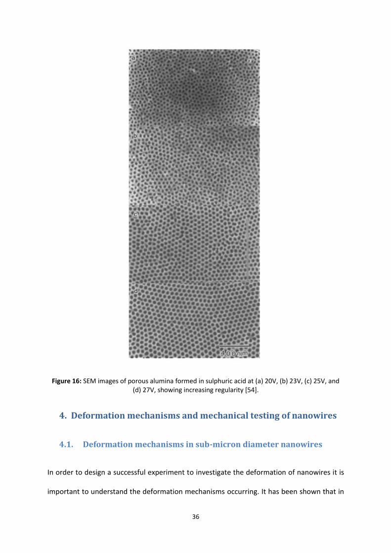
36
Figure 16: SEM images of porous alumina formed in sulphuric acid at (a) 20V, (b) 23V, (c) 25V, and (d) 27V, showing increasing regularity [54].
4. Deformation mechanisms and mechanical testing of nanowires
4.1. Deformation mechanisms in sub-micron diameter nanowires
In order to design a successful experiment to investigate the deformation of nanowires it is
important to understand the deformation mechanisms occurring. It has been shown that in

37
a sub-micron regime, nanopillars strength increase with decreasing diameter [5,7]. The
precise cause of this effect is still unclear, however a number of mechanisms have been
suggested: the storage of geometrically necessary dislocations, dislocation starvation and
limited dislocation nucleation.
4.1.1. Storage of geometrically necessary dislocations
An indentation size effect is well known in the mechanical testing of metals [55–57]. Here
the hardness of the sample during indentation testing increases as the size of the indention
decreases. This effect is more pronounced in the sub-micron indentations. Fleck et al. report
that during indentation the strain directly below the tip of the indenter is large while the
strain far from the tip is zero [58]. This results in a strain gradient across the deformation.
This strain gradient necessitates a density, , of geometrically necessary dislocations
(GNDs). The density of these dislocations increases with the inverse of the length scale (see
Equation 3).
Where is the dislocation density, is the macroscopic plastic shear
stress, is the magnitude of the Burger’s vector and is the local
length scale of the deformation field.
Equation 3
Nix and Gao further this description by stating that the density of GNDs increase with the
inverse of the indentation depth (see Equation 4 and Figure 17) [59].
Where is the dislocation density, is the magnitude of the Burger’s
vector, is the indentation depth and is the angle of the indentation tip.
Equation 4

38
Figure 17: Geometrically necessary dislocations (GNDs) formed by indentation testing [59].
Nix and Gao proceed to show that an increase in the number of GNDs create a hardening
effect responsible for this indentation size effect: The square of the indentation hardness is
proportional to the reciprocal of the indentation depth.
4.1.2. Dislocation starvation and dislocation nucleation
Greer and Nix present an alternative strengthening mechanism in the absence of strain
gradients in small volumes [6,15]. During the deformation of a bulk material, dislocation
motion leads to the multiplication of dislocations through mechanisms such as double cross
slip and Frank-Read sources. This leads to an increased dislocation density and strain
hardening of the material, increasing its yield strength. In a sufficiently small sample such as
nanowires, dislocations can only travel a short distance before coming into contact with a
free surface, due to the large surface area to volume ratio, and annihilating. This reduces
both the number of dislocations in the sample, as well as the possibility of dislocation

39
multiplication, leading to a dislocation-starved state. For further deformation to occur new
dislocations must be nucleated. This requires high stresses, and thus leads to increased yield
strength.
Volkert and Lilleodden provide a further description of this dislocation hardening [16]. In a
bulk material the dislocation density increases during deformation as discussed above. The
increased dislocation density leads to large internal stresses which can activate dislocation
sources. In a dislocation starved state, the internal stresses of the sample will be lower.
Thus, while large samples can have high dislocation density and can more easily reach the
local stresses required for dislocation nucleation, smaller samples have a lower dislocation
density and lower internal stress and as such require higher applied stress to deform.
4.2. Mechanical testing of nanowires
As discussed above in the introduction, nanowires have frequently been shown to increase
in strength with decreasing diameter in the sub-micron regime. Proposed mechanisms for
this effect have been discussed above. Experimentally, various mechanical testing methods
have been used to demonstrate and investigate the effect.
4.2.1. Testing in bending
Wu et al. investigated gold nanowires with diameters ranging from 40nm to 250nm in
bending [60]. Wires were produced using an electrodeposition into porous alumina and
subsequently released from the original substrate and dispersed onto a new substrate
containing FIB milled trenches. Wires found to span the trenches were secured at both ends
by electron beam induced deposition of lines of platinum. An AFM (atomic force
microscope) cantilever was used to place the nanowire under lateral loading. Figure 18

40
shows a schematic of the experimental setup while Figure 19 shows a 200nm sample in
various states of deformation.
Figure 18: Experimental setup of nanowire bending using AFM [60]
Figure 19: AFM (c,d,e) and SEM (f) images of a 200nm gold nanowire before and after plastic deformation [60]

41
Wu reported that, while the young’s modulus, E, of nanowires remain independent of wire
diameter, the yield strength increases up to 100 times that of the bulk with decreasing wire
diameter and ultimate strengths approaching theoretical (E/10) for the smallest wires
tested.
Figure 20: Young’s modulus and Yield strength for various different nanowire diameters under bending [60]

42
The results of this paper agree with the general theory that nanowires strengths increase
with decreasing diameter. However, as the test was performed in bending, large strain
gradients were introduced, which increase with decreasing length scales i.e. wire diameter.
This makes it difficult to differentiate between strain gradient hardening methods and other
true length scale strengthening mechanisms such as dislocation starvation and nucleation.
Thus it is not possible to determine whether a decrease in sample size causes a fundamental
change in deformation mechanisms in the absence of strain gradients.
4.2.2. Nanoindentation
Uchic et al. proposed a mechanical testing method based on traditional uniaxial
compression testing in order to eliminate strain gradients [5]. Here, nickel and nickel alloy
nanopillars between 500nm and 40μm were produced via a FIB milling method. To perform
a compression test, a nanoindentation system was fitted with a flat-punch tip. Compression
tests were performed at displacement rates of between 1nm/s and 5nm/s and single
nanopillars were tested at a time. Uchic reported an increased strength of up to 25 times
the bulk value for the smallest pillars tested (see Figure 21 and Figure 22).

43
Figure 21: Engineering stress strain curves for bulk and FIB milled nickel tested in compression (A) and SEM image of a 20μm nanopillar pre (B)and post (C) deformation [5]
Figure 22: Engineering stress strain curves for bulk and FIB milled Ni3Al-T alloy tested in compression (A) and SEM images of 20μm nanopillars after deformation [5]
Greer and Nix used a similar uniaxial compression testing methodology on single FIB milled
gold nanopillars [15]. The diamond tip was etched off a standard Berkovich indenter leaving
a flat circle with a 9μm diameter. This was used to compress single nanopillars between

44
400nm and 7450nm in diameter at a strain rate of 0.004s-1. Pillars were located using an
optical microscope calibrated to the indenter. Unlike Uchic et al. pillars were subjected to
multiple loading/unloading cycles to ensure elastic unloading. The smallest pillars tested
achieved a yield strength of 550MPa, 18 times that of bulk. Elastic moduli of 43GPa was also
recorded, similar to that of bulk gold of the same crystal orientation.
Figure 23: Stress-strain curves for FIB produced nanopillars showing loading/unloading cycles and increased yield strength with decreased pillar diameter [15].
A similar method of using a flat-punch tip indenter has been used to test the mechanical
properties single FIB milled pillars by other groups [6,16–18,20,22,23,25,27,61,62]. The
method has also been used to test individual pillars produced by an etching of eutectic
method [8]. All of these investigations have shown evidence for the ‘smaller is stronger’
phenomenon. Performing uniaxial compression tests ideally produce no strain gradients in
the sample and are therefore useful to investigate other strengthening mechanisms in the

45
sub-micron regime. However, FIB milled pillars often show at least a small degree of taper in
the side walls of the pillar and so strain gradients are introduce through the length of the
pillar (as discussed in the FIB production method above). Nano-indentation compression
testing is therefore more suitable for nanowires produced in a taper free method.
All the reports discussed above compress only single pillars at a time. This can be time
consuming to test a statistical significant number of pillars. Also, only low aspect ratio pillars
can be tested without the risk of buckling (aspect ratios of between 2 and 3 have been
recommended [32]). There is also a limit on how small flat-punch tip can be created, and in
various methods of production the wires are too close together to be compressed
individually. Dou and Derby compressed a large number of gold and nickel nanowires grown
by electrodeposition into an alumina template in parallel [11,36]. A 10μm diameter
cylindrical diamond flat punch tip was fitted to a nanoindentor system. The diameter of this
was much greater that the diameter of the nanowires (30nm-80nm), and much larger than
the average cell size (that is the average size of template pore plus pore wall) of 100nm.
Therefore it is not possible to test individual wires without removing wires from the
substrate. A Precise ion polish system was used on electrodeposited wires in an alumina
template to create a uniform height for an area of wires. The wires were then compressed
in parallel and SEM images were used to determine the number of wires compressed. Dou
reported that the Young’s modulus of the gold nanowires to be 79.4GPa, very close to that
of polycrystalline gold of 80GPa. The Young’s modulus reported by Dou is comparable to
that of the polycrystalline bulk due to it being the average of many pillars of random
orientations. The wires showed increased yield strength with decreasing wire diameter. The
elastic unloading shows that no collapse or buckling of the wires takes place during testing.

46
This was thought to be due to the stabilising effect of the large density of nanowires. The
stress-strain plots recorded showed few features compared to other nano-indentation
compression plots (performed on single nanopillars). This was attributed to the stress data
being an average of multiple wires (N>1000).
Figure 24: Side view of the Diamond flat punch tip used by Dou and Derby[36]

47
Figure 25: Nanowire forest after compression testing showing residual indentation [36]
Figure 26: Engineering Stress-Strain curves for 30-70nm nanowires tested in compression [11]

48
To conclude, mechanical testing is possible on sub-micron scale samples. To avoid significant
strain gradients effects a uniaxial compression test has been developed and used on a
variety of different nanowires. A nanoindentation machine is fitted with a flat punch tip to
compress either single nanopillars or a forest of nanowires. FIB produced nanopillars can
still have strain gradients across the length of the pillar and so uniaxial compression tests
are best suited to nanowires produced in a taper free method, such as electrodeposition
into a template. All papers discussed above show an increase in yield strength with a
decreased wire diameter.
5. Experimental methods
This project used an electrodeposition into template method to produce nanowires. Porous
anodic aluminium oxide (AAO) films and prefabricated etched ion track polycarbonate were
used as templates.
5.1. Porous anodic aluminium oxide (AAO) templates
A 2 stage anodizing process based on that of Masuda and Fukuda and developed by Dou and
Derby was used to produce regularly ordered aluminium oxide templates [10,11]. The
process is summarised in Figure 27.

49
Figure 27: Schematic diagram showing production stages of AAO template and subsequent
nanowires. i) Aluminium substrate after 1st anodising stage and subsequent oxide removal, ii) 2nd anodising stage and pore widening, iii) Coating with PMMA, iv) Aluminium etched away, v) Oxide
barrier layer etched away, vi) Oxide coated with metal, vii) PMMA removed, viii) metal electrodeposited into pores, ix) Oxide template etched away.

50
Samples were cut from a high purity (99.999%) aluminium sheet to form the substrate
material. The substrates were prepared for electropolishing by degreasing in acetone. The
substrates were then electropolished at 20V for 5 minutes in a 1:4 by volume mixture of
perchloric acid and ethanol (VWR International, Lutterworth, UK; Fisher Scientific,
Loughborough, UK). Care was taken that the solution did not reach above 10°C by
performing the procedure in an ice bath.
The electropolished substrates were anodised in a 0.3M oxalic solution (Fisher Scientific,
Loughborough, UK) for 12 hours at 40V. This produces an aluminium oxide film on the
surface of the substrate as discussed above in section 3. The film microstructures were
characterised using scanning electron microscopy (SEM) (XL 30, Philips, Amsterdam,
Netherlands).
The aluminium oxide film formed by the first anodising stage was removed by chemical
etching in a mixed solution of 0.1M chromic acid and 0.1M phosphoric acid (Fisher Scientific,
Loughborough, UK). This was done at 60°C for 2 hours. SEM images of the ridges formed on
the aluminium were taken.
The second stage of anodising was carried out in conditions identical to the first stage for 2
hours. The anodising time is proportional to the final thickness of porous film. Again, film
microstructures were characterised using SEM.
2g poly methyl methacrylate (PMMA) was dissolved in 20ml acetone and a layer was applied
to the porous alumina using a cotton tip. Once dry the aluminium substrate was removed by
etching in 0.1M copper chloride solution (Fisher Scientific, Loughborough, UK) for 5 hours.
The exposed alumina barrier layer was removed by etching in 0.1M phosphoric acid for 1

51
hour at 30°C. A gold/palladium coating system (Model 682 PECS, Gatan Inc., Pleasanton, CA,
USA) was used to provide a new substrate to support the oxide film, as well as to act as the
cathode during electrodeposition. The thickness of the gold coating must be such that the
pores in the template are completely covered; we estimated a thickness of coating of
approximately equal to that of the pore diameter to be sufficient. Any further coating is
unnecessary, however a thicker layer results in the easier handling of the sample. Finally the
PMMA layer was removed by dissolution in acetone.
5.2. Etched ion track polycarbonate templates
Prefabricated etched ion track polycarbonate filters were purchased in a variety of pore
sizes (100nm, 200nm, 400nm and 800nm) (EMD Millipore Corporation, Billerica, MA, USA).
To prepare the samples for electrodeposition an identical gold/palladium coating process to
that used on the AAO templates was performed. This is the only pre-processing stage
required as the filters already have the pores at the specified diameter.
5.3. Electrodeposition of copper into templates
Once each sample type was gold coated (and the PMMA layer removed in the case of the
AAO template) the further preparation and electrodeposition stages were identical for each
type of template. The template was cut into sample sizes of approximately 0.25cm2. This
was purely for practical reasons as it meant that each template prepared could be used for 4
experiments. The samples were then mounted to a 3cm x 1cm copper sheet. An electrical
contact was made between the copper and the gold/palladium coating by using either silver
conductive paint or conductive SEM sample mount pads. Lacomit lacquer (Xylene, butanol,
Butyl acetone and acetone solution) was used to secure the sample to the copper mount

52
and to cover the rear side and edges of the copper mount to prevent current leakage
through additional electrodeposition occurring in areas other than in the template.
An aqueous solution of 250g/L copper sulphate pentahydrate (CuSO4.5H2O) was used for
electrodeposition. This was based off the finding of Molares et al. and Enculescu et al. who
both reported positive results [44][45]. This is below the solubility limit of copper sulphate
pentahydrate of 316g/L, whilst still providing a large concentration of copper ions for
deposition. Electrodeposition was performed using a potentiostatic method at room
temperature. The Au/Pd coating on the mounted sample served as the target cathode and a
copper anode was used. A calomel reference electrode was also used as a reference. DC
voltages between 1500mV and 200mV were used for time periods ranging from 10s to 300s.
6. Results and discussion
Scanning electron microscopy (SEM) was used to image the etched ion track polycarbonate
templates and an analysis of pore size was carried out. Images of the polycarbonate
templates after electrodeposition were also studied. SEM images at multiple stages of
anodised aluminium oxide template production were taken, as well as images after
electrodeposition. The two different types of templates were compared, as were the
nanowires grown in both templates.

53
6.1. Polycarbonate membrane pore analysis
6.1.1. 800nm template analysis
Four different pore size filters were purchased: 100nm, 220nm, 400nm and 800nm (EMD
Millipore Corporation, Billerica, MA, USA). A scanning electron microscope (SEM) was used
to acquire images of each different pore size. A thin layer of gold/palladium was coated
onto the templates to reduce electron charging within the SEM. This layer was
approximately 3nm thick and so does not significantly affect pore size measurements. A
relatively low accelerating voltage was used to further discourage charging. Figure 28 shows
an SEM image of a template with pores specified at 800nm diameter.
Figure 28: SEM image of 800nm pores in a polycarbonate template. Template has been coated in a
~3nm layer of Au/Pd to avoid electron charging.

54
The pores in the filter are clearly not in a regular order. This is due to the production
method used to produce the filters being similar to that of Molares et al. as discussed above
[43,44]. The polycarbonate films were exposed to radiation bombardment and the damage
tracks were etched to produce pores of the specified diameter. This results in a template
with no pore ordering; some areas of the template have a large concentration of pores and
some areas are devoid of pores. Areas with a large concentration of pores often have
overlapping pores, the effects of this on pore size are revealed once the image is put into
image analysis software.
ImageJ software (ImageJ, U. S. National Institutes of Health, Bethesda, MD, USA) was used
to perform a pore size analysis of the template [63]. The scale of the image was calibrated
using the scale bar included in the original SEM image (Figure 28). A threshold was applied
to convert the image to a black and white binary image (Figure 29). To improve the accuracy
of pore measurement partial pores at the edge of the image, as well as any dark areas of
template picked up by the threshold from the original image were removed by selecting all
particles under a critical diameter; 800nm pores have an area of 0.5μm2 so a value of 0.25
μm2 was selected as a critical diameter to ensure no complete pores were selected (see
Figure 30). Figure 31 shows that no complete pores were removed from the image.

55
Figure 29: 800nm pores after threshold applied to convert image to binary.
Figure 30: 800nm pores after incomplete pores and areas of template were removed.

56
Figure 31: Incomplete pores and dark template removed from Figure 30 showing no complete pores
were removed.
Particle analysis was performed on the remaining black areas, i.e. pores. 528 particles were
analysed, with a mean diameter of 1034nm ± 281nm (standard deviation). Whilst the
quoted value of pore diameter of 800nm is within the standard deviation of the calculated
mean, it is still considerably higher. The standard deviation is 27% the value of the mean.
The reason for both the high mean and large standard deviation is related to the random
nature of pore placement. A large number of pores overlap each other, which ImageJ
interprets as a single large pore. In areas of high pore density multiple pores can overlap to
form a large area. The largest area taken by a single particle during analysis was 4.919μm,
requiring at least 10 overlapping pores at minimal overlap (800nm diameter pores have a
0.5 μm2 area). As no pores have an area a drastically reduced area less than that of a single
pore this pore overlap considerably increases both the mean pore diameter value and the
standard deviation of this value.

57
To accurately measure the size of pores formed from individual etched ion tracks (i.e. pores
where no overlap occurs) a filter is applied to the image. ImageJ was set up to only select
pores with a circularity of at least 0.95. This selects all individual pores and the result is
shown in Figure 32. The image still however includes some overlapping pores. This occurs
when the overlap is almost perfect, or when a number of almost perfect overlaps create a
pore without affecting its circularity. The mean pore diameter from this image is 871nm
with a standard deviation of 51nm. This mean is much closer to the specified value of
800nm, and the standard deviation shows a much lower spread of pore diameters.
Interestingly the specified value is not within the standard deviation of the calculated mean,
unlike in the initial calculation. A possible reason for the larger than specified mean pore
diameter is discussed in the later in this section.
Figure 32: Image of 800nm pores after removal of particles with circularity <0.95. Note small number
of overlapping pores remain.

58
The number of pores in the original sample image used for pore size analysis (Figure 30) was
528. The number of pores with little to no overlap (Figure 32) was 256. The result of this is
that only 48% of nanowires produced will have the desired cylindrical shape and required
diameter. This is extremely relevant when designing an experiment involving mechanical
testing of the nanowires where wire diameter is a critical value.
The porosity of the template was calculated using the image with all pores displayed,
including partial pores at the edge of the image (Figure 29), however dark areas of template
were not included (a filtering process similar to that of Figure 30 was used but with a smaller
limit imposed). A porosity of 20.8% was recorded. This is at the upper limit of the porosity as
quoted in the specifications (see Figure 33). This suggests that either: a) this particular area
of the template has a lower than average number of overlapping pores, as the area of two
individual pores for example would be greater than if there was any overlap between the
two; b) there are a number of pores with an elliptical appearance, and hence a larger area,
due to a non-normal pore angle; c) this particular area of template received a higher than
average radiation dose during manufacture; or else d) this area of template is fairly average
and the lower porosity quoted in the specifications is merely to ensure any filters supplied
with a lower than average radiation dose remain within the parameters.
800nm IsoporeTM Membrane Filters
Chemistry Polycarbonate
Pore size 0.8 μm
Filter diameter 25 mm
Thickness 7 - 22 μm
Porosity 5 – 20 %
Figure 33: Summary of specifications of 800nm pore diameter filters [64].
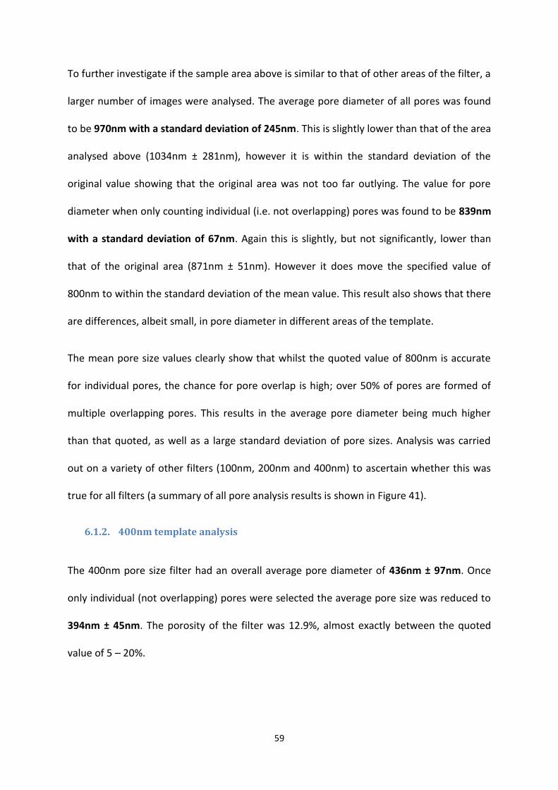
59
To further investigate if the sample area above is similar to that of other areas of the filter, a
larger number of images were analysed. The average pore diameter of all pores was found
to be 970nm with a standard deviation of 245nm. This is slightly lower than that of the area
analysed above (1034nm ± 281nm), however it is within the standard deviation of the
original value showing that the original area was not too far outlying. The value for pore
diameter when only counting individual (i.e. not overlapping) pores was found to be 839nm
with a standard deviation of 67nm. Again this is slightly, but not significantly, lower than
that of the original area (871nm ± 51nm). However it does move the specified value of
800nm to within the standard deviation of the mean value. This result also shows that there
are differences, albeit small, in pore diameter in different areas of the template.
The mean pore size values clearly show that whilst the quoted value of 800nm is accurate
for individual pores, the chance for pore overlap is high; over 50% of pores are formed of
multiple overlapping pores. This results in the average pore diameter being much higher
than that quoted, as well as a large standard deviation of pore sizes. Analysis was carried
out on a variety of other filters (100nm, 200nm and 400nm) to ascertain whether this was
true for all filters (a summary of all pore analysis results is shown in Figure 41).
6.1.2. 400nm template analysis
The 400nm pore size filter had an overall average pore diameter of 436nm ± 97nm. Once
only individual (not overlapping) pores were selected the average pore size was reduced to
394nm ± 45nm. The porosity of the filter was 12.9%, almost exactly between the quoted
value of 5 – 20%.

60
6.1.3. 220nm template analysis
The 220nm filter had an overall average pore diameter of 343nm ± 138nm. Once only
individual (not overlapping) pores were selected the average pore size was reduced to
259nm ± 20nm. The porosity was measured to be 26% (13.8% quoted). The porosity value
for this filter is considerably higher than that quoted. This is at least partially due to the SEM
image analysed (see Figure 34). The image has a notable brightness gradient across the
vertical axis, from darker at the top to lighter at the bottom. As well as this there are areas
of filter that are as dark as the pores. Due to these two effects it was difficult selecting only
pores when applying the threshold converting the image to binary (Figure 35). To get an
acceptable image to analyse, a convolve filter was applied to a copy of the image to create a
blurred version. This image was used as a background to subtract from the original image
eliminating most of the brightness gradient. After this additional processing a threshold
image of all pores was obtained. However, this image still included some unavoidable areas
where part of the filter was selected as pores. This additional area slightly increases the
measured porosity of the filter as this extra area is included.

61
Figure 34: SEM image of 220nm filter. Not brightness gradient from the top of the image (darker) to the bottom of the image (lighter).
Figure 35: SEM image of 220nm pores when attempting to apply a binary threshold, highlighting issues due to a vertical brightness gradient.

62
Figure 36: Threshold image after selecting all pores in 220nm template. Note some areas of filter remain selected, increasing average pore diameter and porosity.
6.1.4. 100nm template analysis
The 100nm pore size filter had an average pore diameter for all pores of 163nm ± 34nm.
Individual (not overlapping) pores had an average pore size of 151nm ± 14nm. The porosity
of the filter was 11.2%, more than double than the quoted value of 4.18%. The image used
had none of the difficulties as described for the 220nm filter and this value is not artificially
increased.
6.1.5. Pore angle
A number of pores in Figure 28 show a brightness gradient across the diameter of the pore,
as well as appearing to have an elliptical cross section. This is caused by the radiation
incident angle, and therefore pore angle, being not normal to the filter surface. The effect is
shown more clearly in Figure 37. The non-perpendicular pore angle can occur in both single

63
pores as well as overlapping pores. Time restraints have limited further investigation (e.g.
side on images) into specific values of the pore angles (as discussed in future studies). This
effect also influences pore diameter and porosity measurements, as it results in an elliptical
pore. However, due to the selection process when measuring non overlapping pores (as
discussed above) being a circularity limit this has a minimal effect on average pore diameter
recorded for single pores.
Figure 37: SEM image showing non-perpendicular pore angle in 800nm polycarbonate template.
6.1.6. Polycarbonate damage susceptibility
It is worth discussing the damage susceptibility of the templates, as handling is required for
both preparing for, as well as during, electrodeposition. After the gold/palladium coating
the filters are cut into quarters (as discussed in experimental methods above). Figure 38
shows the damage caused by a cut. The damage is limited to an area of less than 20μm from
the cut. This shows that the template is suitable to be split into separate samples as the

64
Lacomit lacquer securing the samples to their copper mount cover more than this affected
area.
Figure 38: SEM image of damage during cutting of polycarbonate templates. Damage penetrates up to 20μm from the edge.
The polycarbonate templates remain fragile during handling. Figure 39 shows the damage
caused by handling with a crocodile clip. This damage occurred during an early
electrodeposition run before samples were mounted to a copper sheet, and the damage
influenced the decision to mount the samples.

65
Figure 39: SEM image of damage caused by a crocodile clip during handling.
It is also possible to damage the polycarbonate templates during SEM imaging. Figure 40
shows a dark area in the centre of the image. This is known as specimen contamination and
is caused by residual gas being struck by the electron probe. The dark area shows where an
increased magnification view was used for focussing. Upon reducing the magnification the
area around the previous selection showed significant damage. This is due to stresses
caused by the incoming electrons of the SEM. It is therefore not possible to put imaged
templates to further use.

66
Figure 40: SEM image of damage to a 100nm polycarbonate template due to electron imaging. The dark area at the centre shows where an increased magnification was used for focussing purposes,
with damage around this area.
6.1.7. Summary of etched ion track polycarbonate template analysis
A summary of polycarbonate template properties is shown in Figure 41. Whilst the average
pore diameter for individual pores is close to the specified value, the overall average pore
diameter for each template size when including all pores is considerably greater than that
specified. The standard deviation for each samples is at least 20% that of the mean (100nm
template) and as much as 40% of the mean (220nm template). This large variance in pore
diameter, as well as the fact that the average pore diameter is much greater than that
specified, results in templates unsuitable for the growth of nanowires for many applications
(as discussed later).

67
Specified pore
diameter
Average pore
diameter (only
individual pores) (nm)
Average pore
diameter (all pores)
(nm)
Specified porosity Measured
porosity
800nm 839 ± 67 970 ± 245 5 – 20% 20.8%
400nm 394 ± 45 436 ± 97 5 – 20% 12.9%
220nm 259 ± 20 343 ± 138 13.8% 26%*
100nm 151 ± 14 163 ± 34 4.18% 11.2%
Figure 41: Table showing summary of pore analysis measurements. *porosity value for 220nm
template artificially inflated (see above).
6.2. Electrodeposition into polycarbonate membrane
Electrodeposition into the etched ion-track polycarbonate templates was carried out of a
range of potential values and time scales. All electrodeposition was carried out using a
250g/L copper sulphate pentahydrate (CuSO4.5H2O) solution, with a copper anode, a
saturated calomel reference electrode and the sample as the cathode. Only the 800nm pore
size template was used due to time restrictions. Significant results are discussed below.
6.2.1. Sample 1
Figure 42 shows a sample after electrodeposition for 300 seconds at an offset potential of -
1500mV. The majority of pores are unfilled, and the few that are show growth only on the
side walls of the pores. It was thought that this was due to an insufficient thickness of the
gold/palladium coating. If this coating was too thin, the pores would not be completely
covered. The copper would therefore be begin to be deposited at the edge of the pore
bottom and proceed to grow vertically through the pore, resulting in the partially filled
pores observed. A magnified view of this effect is shown in Figure 44 (taken from a separate
sample). Energy-dispersive X-ray spectroscopy was used to analyse the elemental
composition of the sample surface (Figure 43). The spectrum showed low copper peaks,
proving that copper had been deposited, if only in limited amounts.

68
Figure 42: SEM image of 800nm template after copper electrodeposition at an offset potential of -1500mV for 300 seconds. The majority of pores are unfilled.
Figure 43: Energy-dispersive X-ray spectroscopy spectrum for copper electrodeposited in
polycarbonate template (Figure 42). Small copper peaks are shown, due to limited amount of copper deposited.

69
Figure 44: SEM image partially filled pores in an 800nm template after copper electrodeposition at an offset potential of -1500mV for 300 seconds.
6.2.2. Sample 2
Following the results above, a thicker conductive gold/palladium layer was applied to
subsequent samples. Electrodeposition was repeated using the same parameters as above
(potential difference of -1500mV for 300s). The result of this is shown in Figure 45. This
image shows a range of different results. Some pores are partially filled like those discussed
above in the previous sample. Conversely, there are large deposits formed on the surface of
the template. These were confirmed to be copper by Energy-dispersive X-ray spectroscopy
and a reduced brightness view is shown in Figure 46. Caps are formed once a pore has been
completely filled with copper (as discussed above in the literature review, and by Molares et
al. [43,44]). It is energetically favourable to continue growth at a current nucleation point
than to nucleate new growth areas. Therefore, the earliest pores to begin filling will proceed
at a quicker rate than others. Once the pore is full copper growth is free of the size
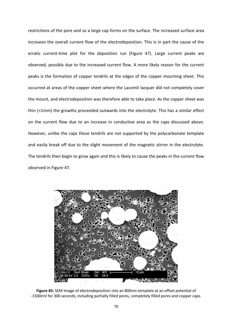
70
restrictions of the pore and so a large cap forms on the surface. The increased surface area
increases the overall current flow of the electrodeposition. This is in part the cause of the
erratic current-time plot for the deposition run (Figure 47). Large current peaks are
observed, possibly due to the increased current flow. A more likely reason for the current
peaks is the formation of copper tendrils at the edges of the copper mounting sheet. This
occurred at areas of the copper sheet where the Lacomit lacquer did not completely cover
the mount, and electrodeposition was therefore able to take place. As the copper sheet was
thin (<1mm) the growths proceeded outwards into the electrolyte. This has a similar effect
on the current flow due to an increase in conductive area as the caps discussed above.
However, unlike the caps these tendrils are not supported by the polycarbonate template
and easily break off due to the slight movement of the magnetic stirrer in the electrolyte.
The tendrils then begin to grow again and this is likely to cause the peaks in the current flow
observed in Figure 47.
Figure 45: SEM image of electrodeposition into an 800nm template at an offset potential of -1500mV for 300 seconds, including partially filled pores, completely filled pores and copper caps.

71
Figure 46: SEM image of copper caps formed on a polycarbonate template.
Figure 47: Current-Time plot of copper electrodeposition into 800nm polycarbonate template at
-1500mV. Note: Current density values are for indication only due to the lack of accurately measuring electrodeposition area (especially during cap or tendril growth, See section 6.2.3).

72
6.2.3. A note on current density-time plots
The potentiostatic set up used recorded of current density with time rather than current. In
order to calculate a current density the software required a surface area value be inputted.
As the samples used were not a regular size, were secured by an area of lacquer, and the
templates had a porosity value, this deposition area was estimated. The area was
approximated to a square with sides of 0.5cm (the software was calibrated in centimeters),
and the porosity was assumed to be 20%. This resulted in a value of 0.05cm2. However, as
caps or tendrils grow on the sample the area increases, which increases current flow. As this
change in area is not taken into account by the software, and the increase in current is
displayed as an increase in current density. It is therefore advisable to interpret the current-
time plots as a representation of current flow, and not to use actual current density values.
6.2.4. Sample 3
The large caps grown on the surface of the previous sample suggest that the
electrodeposition time was too long. Ideally the electrodeposition process would end before
the caps start to form. Figure 48 shows the results of electrodeposition into a template for
60 seconds at the same potential as used previously (-1500mV). The reduction in
electrodeposition duration drastically reduces the number of caps grown, with the majority
of the template surface being cap free. The image shows a mixture of unfilled, partially filled
and full pores. A possible reason for the uneven pore filling rate in the sample is undesirable
reactions taking place in some of the pores. If the current supplied is too high it is possible
to deplete the solution inside the pores. This will cause hydrogen from the solution to
reduce in place of the copper. The hydrogen can build up and form bubbles, causing
reduced or no copper deposition to take place in that pore. Mechanical stirring of the

73
solution can reduce the hydrogen buildup, however there is minimal flow at the bottom of
the pores. The pores where hydrogen reduction occurs will have a lower chance of copper
nucleation, whilst other pores may be fully filled.
Figure 48: SEM image of electrodeposition into an 800nm template at an offset potential of -1500mV for 60 seconds, showing full and partially filled pores.
6.2.5. Sample 4
To increase the number of filled pores the applied potential was reduced, thereby reducing
(and ideally eliminating) hydrogen evolution. Figure 49 shows a much increased ratio of
filled pores to empty pores (approximately 90% filled). This was achieved using an offset
potential of -1000mV for 60 seconds. Despite the reduced potential and hence lower
electrodeposition rate, the time period was not increased. This was to ensure that no caps
were grown on the surface of the template. The pores were shown to be comprised of
copper by energy-dispersive X-ray spectroscopy (Figure 50). The spectrum shows large
peaks corresponding to the Lα and Kα values for copper. Large sulphur peaks are also
present, due to the copper sulphate pentahydrate electrolyte. The brightness of each pore

74
corresponds to the height of the nanowire grown within the pore. A large amount of pores
are the same height, approximately that of the thickness of the template. Time restraints
however meant no profile image of the wires could be taken to fully study wire height
Figure 49: SEM image of electrodeposition into an 800nm template at an offset potential of -1000mV for 60 seconds (for clarity: scale bar reads 20μm and magnification reads 1501x).
Figure 50: Energy-dispersive X-ray spectroscopy spectrum of polycarbonate template sample 4 (Figure 49). Large copper peaks are present confirming copper deposition.

75
The current-time plot for this sample has none of the peaks associated with large increase
then decrease in electrodeposition area. This corresponds with the fact that tendrils were
not observed to grow on the sample. The increase in current throughout the deposition
suggests an increase in deposition area. This is supported by theory, which states that
nucleation is more likely to begin at the interface between the pores and the gold/palladium
coating at the bottom of the pores. The reduced surface area required here reduces the
energy cost of nucleation, causing preferential nucleation to occur. The growth of copper
from these points along the sides of the pore increases the electrodeposition area. Thus
complete pores are likely to be formed when multiple edge growths combine. This results in
polycrystalline wires, a result confirmed by comparing the caps formed with those produced
by Molares et al. shown in Figure 11, which are of a circular nature rather than the multi-
faceted caps associated with single-crystal wires [43]. Further crystallographic analysis could
be used to confirm the structure of the wires, but was not performed due to time restraints.
Figure 51: Current-Time plot of copper electrodeposition into 800nm polycarbonate template at
-1000mV. Note: Current density values are for indication only due to the lack of accuracy in measuring electrodeposition area.

76
6.2.6. Summary of electrodeposition into polycarbonate templates
Electrodeposition into polycarbonate templates was performed at potentials of between -
1500mV and -1000mV for time periods ranging from 15s to 300s. The best results were
found when performed at -1000mV for 60 seconds. The wires produced filled the majority
of the pores (approx. 90%) and were of a fairly uniform height, as demonstrated by SEM
images. Increasing the current (by increasing the potential) results in a lower pore filling
ratio, most likely due to hydrogen reduction in some pores. Grown nanowires were shown
to be polycrystalline in structure, as shown by the circular caps formed on the surface of the
template under longer electrodeposition.
6.3. Aluminium Oxide template growth
A two-stage anodizing process by Masuda et al. and developed by Dou and Derby was used
to produce ordered anodised aluminium oxide (AAO) templates [10,11]. An analysis of the
templates created is presented following.
6.3.1. First stage anodisation
After electropolishing, the aluminium substrate is much less rough than that of the original
aluminium, however there remain features such as ridges on the surface (time restraints
prevented analytical methods such as AFM (atomic force microscopy) being used to
determine surface morphology). After a long-period anodizing (12h) in 0.3M oxalic acid at
40V an alumina oxide film is formed on the surface. Figure 52 shows the surface of the
sample after this first anodizing stage. The pores formed are not in any regular order,
despite the self-ordering nature of porous alumina due to space restraints [50]. The average

77
pore size is 1640nm ± 420nm. This is larger than suggested by literature, and the
distribution in size is fairly large [10]. The reason for the lack of regularity and large pore size
distribution is the large thickness of the oxide layer causing various distortions [9].
Figure 52: SEM image of alumina film after 12h anodising in 0.3M oxalic acid at 40V.
6.3.2. Ridges formed on aluminium
The thick, distorted layer of oxide was removed by etching in a 0.1M Chromic acid and 0.1M
phosphoric acid solution. The anodizing process causes ridges to form on the aluminium
substrate, as shown in Figure 53. The ridges form cells and are highly ordered. ImageJ was
used to determine the pore size by a similar process to that described for the polycarbonate
templates. The pores were found to be 61.5nm ± 3.1nm, showing a low degree of size
distribution. The cell interval (pore center to pore center) distance was found to be 112.5nm
± 11.5nm. This result agrees with analysis performed on images taken by Dou, of 64.2nm ±
8.0nm and 105.4nm ± 8.6nm respectively [36]. Time restraints prevented the depth of the
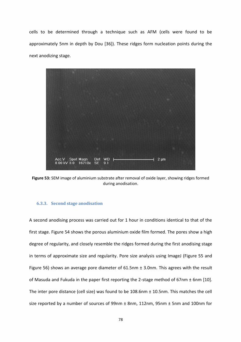
78
cells to be determined through a technique such as AFM (cells were found to be
approximately 5nm in depth by Dou [36]). These ridges form nucleation points during the
next anodizing stage.
Figure 53: SEM image of aluminium substrate after removal of oxide layer, showing ridges formed during anodisation.
6.3.3. Second stage anodisation
A second anodising process was carried out for 1 hour in conditions identical to that of the
first stage. Figure 54 shows the porous aluminium oxide film formed. The pores show a high
degree of regularity, and closely resemble the ridges formed during the first anodising stage
in terms of approximate size and regularity. Pore size analysis using ImageJ (Figure 55 and
Figure 56) shows an average pore diameter of 61.5nm ± 3.0nm. This agrees with the result
of Masuda and Fukuda in the paper first reporting the 2-stage method of 67nm ± 6nm [10].
The inter pore distance (cell size) was found to be 108.6nm ± 10.5nm. This matches the cell
size reported by a number of sources of 99nm ± 8nm, 112nm, 95nm ± 5nm and 100nm for

79
identical anodizing conditions [10][65][38][53]. The cell size to voltage proportionality
coefficient of 2.7nm/V also corresponds with that reported by Li et al. of 2.8nm/V [12].
These values confirm the oxide layer’s resemblance to the ridges formed in the previous
stage, with both parameters being similar (pore size of 61.5nm ± 3.0nm compared to pore
size of 61.5nm ± 3.1nm for the ridges, and cell size of 108.6nm ± 10.5nm compared to
112.5nm ± 11.5nm of the ridges). This provides evidence for the ridges being nucleation
points for the oxide formation on the surface of the aluminium, and also suggests that the
pores formed are straight and parallel. The appearance of the inside of the pores being fully
dark with no shadow supports this, as the inside of angled pores would be visible. Time
restraints prevented profile images of the templates to be taken so this could not be
experimentally verified. Profile images would also be used to determine the thickness of the
oxide layer and the depth of the pores. The porous aluminium oxide has been reported to
have a growth rate of 220nm/min, which suggests a thickness in this case of 13.2μm [36].

80
Figure 54: SEM image of porous aluminium oxide formed after second anodising process showing similar appearance to the ridges formed during the first anodising stage (Figure 53).
Figure 55: SEM image of porous aluminium oxide formed after second anodising process used for pore analysis (higher magnification results in an increase in accuracy).
Figure 56: Image of pores after ImageJ threshold and particle analysis applied to Figure 55.

81
6.4. Electrodeposition into AAO templates
Prior to electrodeposition, the templates produced required further processing stages.
These are discussed in the experimental methods, but in summary are: coating with PMMA,
etching of aluminium, etching of oxide barrier layer, porous alumina coated with
gold/palladium, removal of the PMMA. Electrodeposition took place in a 250g/L copper
sulphate pentahydrate (CuSO4.5H2O) solution identical to that used for the polycarbonate
templates. A copper anode and saturated calomel reference electrode were used, with the
gold/palladium of the sample used as the cathode. As with the polycarbonate templates,
significant results are discussed below.
6.4.1. Sample 1
Following the positive results reported above for the polycarbonate template sample 4,
similar electrodeposition parameters were used to deposit into the porous alumina
template. A potential difference of -1000mV was applied. The time period was reduced to
30 seconds to prevent caps forming due to the template being thought to be thinner than
the polycarbonate (approx. 13.2μm compared to 20μm). Figure 57 shows the surface of the
template after electrodeposition. Large angular growths up to 20μm in length are evident
on the template surface. The angular nature of the growths suggests that single crystal
nanowires were grown beneath them (see Figure 11). The pores here are much narrower
than those in the polycarbonate template and so multiple nucleation points in each pore are
less likely, supporting the suggestion of single crystal growth. The growths were confirmed
to be copper using Energy-dispersive X-ray spectroscopy (Figure 58). The spectrum shows a
low copper peak however, indicating a low amount of copper deposited. Peaks representing

82
gold and palladium are present due to a thin (~3nm) Au/Pd coating applied prior to SEM
imaging to prevent electron charging on the surface of the alumina.
Figure 57: SEM image of the surface of porous alumina template sample 1, showing angular copper growths.
Figure 58: Energy-dispersive X-ray spectroscopy spectrum of aluminium oxide sample 1 (Figure 57).
Small copper peaks indicate low amount of copper deposited.
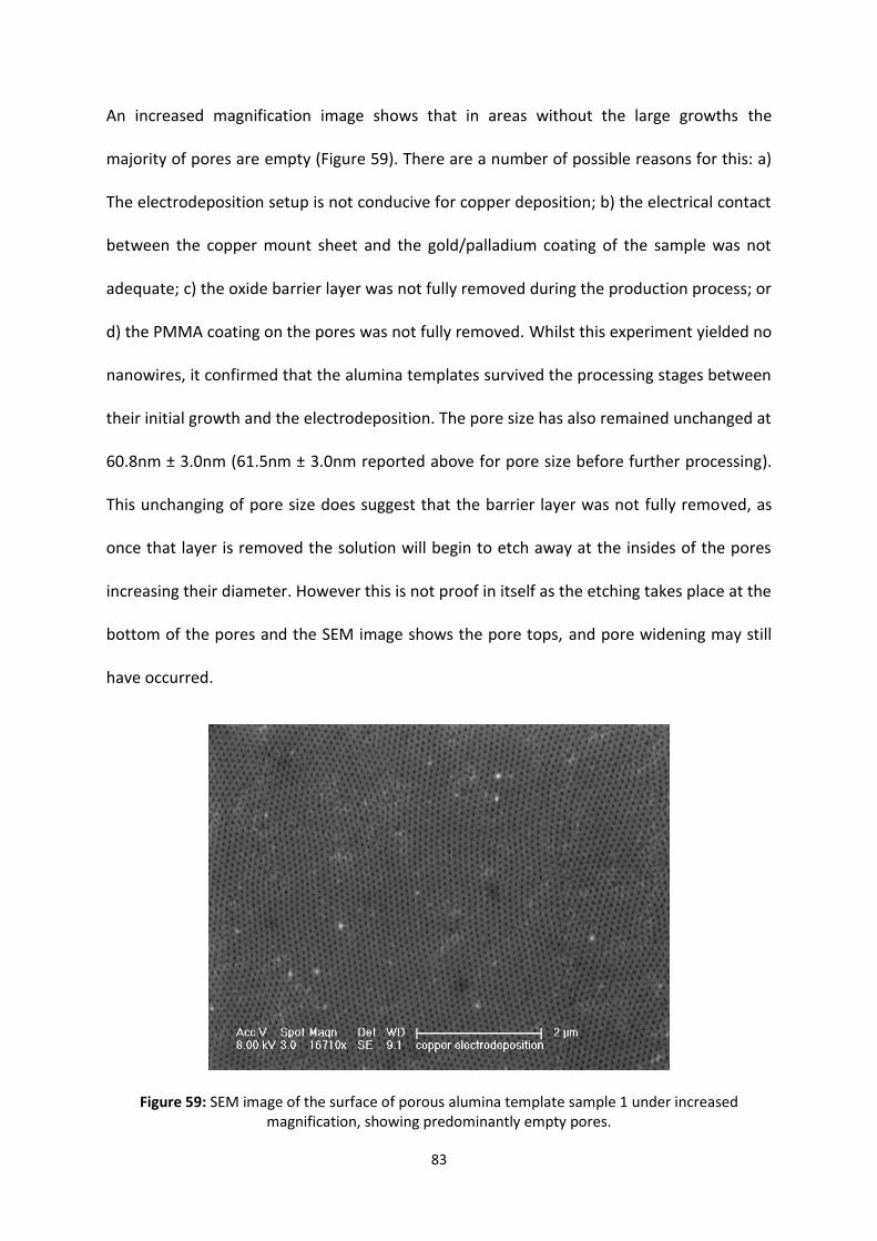
83
An increased magnification image shows that in areas without the large growths the
majority of pores are empty (Figure 59). There are a number of possible reasons for this: a)
The electrodeposition setup is not conducive for copper deposition; b) the electrical contact
between the copper mount sheet and the gold/palladium coating of the sample was not
adequate; c) the oxide barrier layer was not fully removed during the production process; or
d) the PMMA coating on the pores was not fully removed. Whilst this experiment yielded no
nanowires, it confirmed that the alumina templates survived the processing stages between
their initial growth and the electrodeposition. The pore size has also remained unchanged at
60.8nm ± 3.0nm (61.5nm ± 3.0nm reported above for pore size before further processing).
This unchanging of pore size does suggest that the barrier layer was not fully removed, as
once that layer is removed the solution will begin to etch away at the insides of the pores
increasing their diameter. However this is not proof in itself as the etching takes place at the
bottom of the pores and the SEM image shows the pore tops, and pore widening may still
have occurred.
Figure 59: SEM image of the surface of porous alumina template sample 1 under increased magnification, showing predominantly empty pores.

84
6.4.2. Sample 2
During electrodeposition of the previous sample, the electrodeposition parameters and set-
up were identical to that of the successful polycarbonate template deposition and so the
incorrect electrodeposition conditions suggestion can be discounted. The electrical contact
from the mount to the sample is sufficient enough to support the large copper growths and
so was not thought to be the cause of low yield of nanowires. Finally there was no evidence
of any remaining PMMA on the surface of the sample from the SEM images. During the
production of the subsequent templates a longer period phosphoric acid etch was used to
ensure the entirety of the barrier layer was removed. Figure 60 shows the result of
electrodeposition into a porous alumina oxide template using the same electrodeposition
parameters: -1000mV potential for 30 seconds. Here, large bulbous copper growths are
observed, in contrast to the angular growths observed in the previous sample. Referring to
Figure 11, these growths suggest a polycrystalline structure. The growths were again
confirmed to be copper by energy-dispersive X-ray spectroscopy (Figure 61). An explanation
for these growths could be that a number of nanowires have grown in close proximity to
one another, caps formed on the alumina surface and new copper growths have nucleated
on these caps. Hence it is difficult to ascertain whether the wires themselves are of single or
polycrystalline structure, and without removing the caps and performing further
crystallographic analysis it is not possible to tell. The current-time plot for this run shows a
continuous increase in current, reflecting the increase in electrodeposition area. Areas
without the large growths show an almost zero pore filling rate as in the previous sample
(Figure 63).

85
Figure 60: SEM image of the surface of porous alumina template sample 2, showing large circular copper growths (scale bar 20μm).
Figure 61: Energy-dispersive X-ray spectroscopy spectrum of growths on aluminium oxide sample 2 (Figure 60).

86
Figure 62: Current-time plot for alumina oxide template sample 2 showing continuous increase in
current flow.
Figure 63: SEM image of the surface of porous alumina template sample 2 at higher magnification, showing empty pores.

87
6.4.3. Sample 3
The previous sample was etched for a longer time period, ensuring that the alumina oxide
barrier layer was completely removed. Whilst the sample showed large amounts of copper
deposited, no pores were observed (with the exception of those presumably under the
growths). The energy-dispersive X-ray spectroscopy spectrum for the previous sample
showed a slight carbon peak. This peak is clearer when viewing the spectrum for an area of
the template with fewer copper growths (Figure 64). This may indicate that some PMMA
may remain in the pores, preventing electrodeposition in those pores. In order to
investigate this, a new technique for removing the PMMA was used. Previously the PMMA
was removed by submersing the sample in a beaker of acetone. It is possible therefore
possible for the region near the sample surface to become fully saturated with PMMA whilst
there is still some PMMA in the pores. A new removal method was developed utilizing a
magnetic stirrer and refreshing the acetone during the process.
Figure 64: Energy-dispersive X-ray spectroscopy spectrum of an area with little copper growths on aluminium oxide sample 2, showing carbon peak.

88
Electrodeposition was performed on the sample under similar conditions to the previous
samples (potential of -1000mV for 30s). SEM images of the sample surface following
deposition showed regions of empty pores along with regions with a high pore filling ratio
(Figure 65). The full pores were shown to contain copper by Energy-dispersive X-ray
spectroscopy (Figure 66). Interestingly the peaks for carbon are still present. The average
wire diameter of wires grown was calculated to be 58.0nm ± 5.4nm, comparable to that of
the pore diameter. It is unclear why certain areas were more successful than others in
electrodeposition and further investigation is required.
Figure 65: SEM image of the surface of porous alumina template sample 3, showing region of high pore filling surround by a region of empty pores.

89
Figure 66: Energy-dispersive X-ray spectroscopy spectrum of an area of full pores, showing copper peaks.
6.4.4. Summary of electrodeposition into porous aluminium oxide templates
Electrodeposition was carried out at a potential of -1000mV for 30 seconds in a 250g/L
copper sulphate pentahydrate (CuSO4.5H2O) solution. Despite this set up being successful in
growing nanowires in etched ion track polycarbonate templates it was less efficacious when
used with porous alumina templates. A series of production stages were changed to
investigate possible reasons for the lack of deposition, including increased etching of the
alumina barrier layer and improved removal of the PMMA coating. Improving these two
methods results in a template with areas of high pore filling ratio, surrounded by areas with
empty pores. It is clear that more research into the preparation of alumina templates for
electrodeposition is required. Despite the lack of large areas of nanowires grown, the SEM
images show a positive result in that the porous templates formed after the second
anodising stage successfully survived the further preparation stages and the pore diameter
remains unchanged through these processes.

90
6.5. Etched ion track polycarbonate templates vs. AAO templates
A comparison of both types of template and of the nanowires produced in the templates
follows. The requirement of the wires to be mechanically tested by uniaxial compression is
considered.
Etched ion-track polycarbonate templates have a number of disadvantages due to the way
they are produced. Pores are arranged randomly, with areas of high pore density as well as
areas devoid of pores. This makes compression testing of nanowires produced difficult
whilst the wires remain attached to the substrate. Compression of individual wires is
dependent on being able to identify and locate a wire, and on the removal of all surrounding
wires. Meanwhile the simultaneous testing of multiple wires may result in buckling due to
the lack of stabilising effect from a large density of wires. Nanowires grown in porous
alumina templates are of a highly ordered nature and as such are suitable for mechanical
testing by simultaneous compression as shown by Dou and Derby [11]. The removal of wires
from the substrate for individual testing is possible in both cases; however it is difficult to
perform uniaxial compression or tension tests with free wires.
The diameter of produced nanowires is obviously highly critical during testing of how the
mechanical properties vary with diameter. Thus it is important to have a large degree of
consistency in this parameter. The pores in the polycarbonate templates have a large
standard deviation, as much as 40% the mean value. Due to the random pore arrangement
many pores (over 50%) are in fact multiple overlapping pores, which increases the pore
diameter as well as giving the pore a non-regular shape. The shape can introduce stress
concentration areas in the nanowire which could change its mechanical properties. Contrary
to this, porous alumina templates have a low variation in pore size, with the standard

91
deviation being less than 5% of the mean. This makes the nanowires grown in the
polycarbonate templates unsuitable for mechanical testing, whereas nanowires grown in
alumina templates are valid.
Investigation of how mechanical properties vary with diameter requires a range of
diameters be available. Both templates presented are suitable for an etching process
widening the diameter, using phosphoric acid for the alumina templates and a sodium
hydroxide aqueous solution for polycarbonate [11,66]. Moreover multiple diameters of
polycarbonate filters are available without the requirement for further processing.
For accurate compression testing of the produced nanowires, the nanowires must be
parallel to each other and at a normal angle to the compression axis. A substantial number
of pores (approximately 25% in Figure 37) in the polycarbonate templates were observed in
SEM images to have a non-perpendicular pore angle. This would cause the produced
nanowires to have the same angle, affecting mechanical testing results. Pore angles for the
alumina templates appear in SEM images to be normal to the surface, a result supported by
the matching pore diameters of the ridges in the aluminium and the final measured pore
diameters, as well as the high pore density (which create geometric constraints on the pore
angle). Literature also supports this assumption [65]. However, further investigation is
required to confirm the pore angles for each template.
If the aspect ratio of the wires requires increasing, a thicker template is needed. Shorter
wires can be grown in larger templates by reducing the electrodeposition time. Alumina
templates can be as thick as required, with templates up to 160μm produced [65]. There
have been no investigations into the upper limit of this growth whilst keeping the pores
produced straight and parallel however. Contrary to this, the polycarbonate templates are

92
only available in a specific thicknesses (up to 30μm, depending on pore diameter) and so
this is a limiting factor in the length of nanowires grown [64].
Results from the electrodeposition experiments indicate that whilst porous alumina oxide
templates can be consistently produced through the 2-stage anodising process, there is
further research required into preparing the templates for electrodeposition. This is shown
by the unreliable electrodeposition of nanowires. The large number of processing stages
mean that it is difficult to ascertain which stage the complications arise. The polycarbonate
templates have a much simpler processing route, simply requiring a conductive coating, and
this is reflected in the more consistent electrodeposition results (i.e. pores were filled to
some degree in each experiment).
7. Conclusion
A literature review was performed concluding that a promising method of producing
nanowires without the taper and ion damage associated with focussed ion beam (FIB)
milling, and without the size restraints of an etching of a directionally solidified eutectic, is
electrodeposition into a template. Research into the production of highly ordered porous
anodised aluminium oxide templates was carried out. Finally research into mechanical
testing methods took place. Uniaxial testing was shown to important in testing nanowires
mechanical properties in the absence of strain gradients.
Characterisation of polycarbonate templates was carried out. Templates with a specified
800nm pore diameter were found to have an average pore diameter of 970nm with a
standard deviation of 245nm. This is considerably higher than the specified diameter and
the variation in pore diameter was large (25% the mean). Similar results were found for

93
400nm, 220nm and 100nm templates, with average pore sizes being much higher than the
specified mean with large standard deviations of up to 40% the mean (for 220nm
templates). The reason for the large averages and variation in pore diameters is the large
number of overlapping pores (over 50% of all pores). This also creates pores with a non-
circular cross section, possibly affecting mechanical properties. This result, combined with
the evidence of pores at a non-normal angle to the template surface show that the
polycarbonate templates are not suitable for uniaxial compression testing of nanowires.
Porous anodised aluminium oxide templates were produced through a two-step anodising
process. Pore analysis was performed showing pores to be 61.5nm ± 3.0nm. This matches
templates grown using the same anodising conditions reported in literature. There was a
much lower variation in pore diameters compared to the polycarbonate templates. SEM
images suggested that the pores were straight, parallel with no non-normal pore angles.
Literature further supports this; however this was not experimentally verified duo to time
constraints. The pores are also regularly ordered over a long scale, and as such the
nanowires grown using these templates would be more conducive for mechanical testing via
simultaneous uniaxial compression.
Potentiostatic electrodeposition of copper into the polycarbonate templates was carried out
in a 250g/L copper sulphate pentahydrate (CuSO4.5H2O) solution, with a copper anode, a
saturated calomel reference electrode and using the samples as a cathode. A pore filling
rate of approximately 90% was achieved when applying a potential difference of -1000mV
for 60 seconds. The nanowires grown were shown to be copper using energy-dispersive X-
ray spectroscopy. Using the same parameters when depositing into porous alumina
templates produced less satisfactory results. This was thought to be due to complications

94
arising during one of the production stages between initially producing the porous template
in during the second anodising stage and the electrodeposition. The porous structure was
consistently shown to be intact after electrodeposition with no change in pore size.
Nanowires grown by electrodeposition into etched ion-track polycarbonate templates are
not suitable for the investigation of mechanical properties. This is due to their inconsistent
pore diameter, unordered pore arrangement and varying pore angle. However,
electrodeposition into porous anodised aluminium oxide templates is a promising method
of growing nanowires for this purpose. Pores have a low distribution in diameter, are
regularly ordered and the pores are normal to the template surface. This makes mechanical
testing of the grown nanowires properties possible via simultaneous uniaxial compression
testing.
8. Future works
A key future investigation is into improving the pore filling ratio during electrodeposition.
The preparation stages of the aluminium oxide templates need refining, for example
ensuring all the barrier layer oxide and PMMA layer are removed. Improvements to the
electrodeposition experimental set up could also be investigated. A conical anode could be
used, as a flat anode caused preferential deposition in border areas of the cathode [44].
Additions in the electrolyte could also be considered. Multiple papers have reported using a
small (21g/L – 32g/L) sulfuric acid additions, which are reported to increase the conductivity
of the solution and lower the cathode overvoltage [44,45]. Changes to the electrodeposition
parameters such as potential could also be investigated. During deposition into the
polycarbonate templates, the potential was reduced to avoid hydrogen reduction at the

95
cathode. This could still be occurring at the lower potentials used. Copper has been
reported to have been deposited at potentials as low as -20mV, however time periods
should be increased to compensate for the lower deposition rate [44].
During this work a DC deposition methodology has been used. This was the simplest method
of deposition into the polycarbonate templates, and was used for the alumina templates to
enable comparison between the two. However, the DC method requires many additional
processing steps, including the removal of the aluminium substrate and removal of the
alumina barrier layer. An AC deposition method after the thinning of the barrier layer, such
as that used by Gelves et al. could eliminate these additional stages (see Figure 9) [37].
Gelves performed the anodizing in sulfuric acid however so further investigations into this
process using oxalic acid is required.
The pore angles were not fully characterized during this project. The angles of the pores
were investigated by top down SEM images, however further investigation via profile
images is necessary to fully describe the templates.
The investigation of the relationship between nanowire size and its yield strength requires
the production of nanowires with various diameters. This can be achieved using the alumina
templates through etching of the pores. Investigations into the etching rate of different
chemicals would be useful.
The objective of this project was to compare different methods of producing nanowires for
mechanical testing. An important future study would be these mechanical tests. Nanowires
grown in the porous alumina templates are suitable for simultaneous uniaxial compression
using a flat punch tip fitted nanoindentor. Copper nanowires grown by electrodeposition

96
have not been mechanically tested and so it is important to see if the scaling law suggested
by Dou and Derby applies [7]. Furthermore, the templates are suitable for the growth of a
large range of different metals, as long as the alumina is not reactive to the
electrodeposition solution. Therefore a large number of different metals could be tested.
The micromechanics of strengthening and deformation mechanisms of the nanowires could
be investigated by transmission electron microscopy (TEM).
An additional study could look at the effects of radiation on nanowires. Recent theoretical
work involving nanoporous metals, which have a very similar diameter length scale to metal
nanowires, has suggested that such metallic nanostructures should be highly resistant to
radiation damage [67]. There is a need for such radiation resistant metals for future
applications in nuclear fission and fusion power plants. Thus underpinning research into
deformation mechanisms and the influence of radiation damage on the mechanical
properties of a variety of nanowires, leading to studies of tungsten nanowires could be
performed.
Finally, an investigation to look at thermal effects on BCC nanowire deformation could be
performed. Unlike FCC structured metals, BCC metals do not have a close packed plane, and
for this reason their slip planes are thermally activated. Higher temperatures activate more
slip systems and screw glide mechanisms. Temperature dependant deformation behaviour
could be tested using an elevated temperature nanoindentor.

97
References
[1] Hall EO. Proceedings of the Physical Society Section B 1951;64:747.
[2] N. J. Petch. Journal of the Iron and Steel Institute 1953;174:25.
[3] Gertsman VY, Hoffmann M, Gleiter H, Birringer R. Acta Metallurgica et Materialia 1994;42:3539.
[4] Brenner SS. Journal of Applied Physics 1956;27:1484.
[5] Uchic MD, Dimiduk DM, Florando JN, Nix WD. Science (New York, NY) 2004;305:986.
[6] Greer JR, Oliver WC, Nix WD. Acta Materialia 2005;53:1821.
[7] Dou R, Derby B. Scripta Materialia 2009;61:524.
[8] Bei H, Shim S, George EP, Miller M, Herbert E, Pharr GM. Scripta Materialia 2007;57:397.
[9] Masuda H, Satoh M. Japanese Journal of Applied Physics 1996;35:L126.
[10] Masuda H, Fukuda K. Science (New York, NY) 1995;268:1466.
[11] Dou R, Derby B. Scripta Materialia 2008;59:151.
[12] i AP, M ller , Birner A, ielsch , G sele . ournal of Applied Physics 1998;84:6023.
[13] Uchic MD, Dimiduk DM, Florando JN, Nix WD. MRS Proceedings 2002;753:BB1.4.
[14] Giannuzzi LA, Stevie FA. Introduction to Focused Ion Beams: Instrumentation, Theory, Techniques, and Practice. Springer; 2005.
[15] Greer JR, Nix WD. Applied Physics A 2005;80:1625.
[16] Volkert CA, Lilleodden ET. Philosophical Magazine 2006;86:5567.
[17] Shan ZW, Mishra RK, Syed Asif S a, Warren OL, Minor AM. Nature materials 2008;7:115.
[18] Schneider AS, Clark BG, Frick CP, Gruber P a., Arzt E. Materials Science and Engineering: A 2009;508:241.
[19] Schneider AS, Clark BG, Frick CP. MRS Proceedings 2009;1185:1.
[20] Kim J-Y, Jang D, Greer JR. Acta Materialia 2010;58:2355.
[21] Kim J-Y, Jang D, Greer JR. Scripta Materialia 2009;61:300.
[22] Kim J-Y, Greer JR. Acta Materialia 2009;57:5245.

98
[23] Kim J-Y, Greer JR. Applied Physics Letters 2008;93:101916.
[24] Han SM, Bozorg-Grayeli T, Groves JR, Nix WD. Scripta Materialia 2010;63:1153.
[25] Greer JR, Nix WD. Physical Review B 2006;73:1.
[26] Brinckmann S, Kim J-Y, Greer JR. Physical Review Letters 2008;100:1.
[27] Frick CP, Clark BG, Orso S, Schneider AS, Arzt E. Materials Science and Engineering: A 2008;489:319.
[28] Kraft O, Gruber P a., Mönig R, Weygand D. Annual Review of Materials Research 2010;40:293.
[29] Kiener D, Motz C, Rester M, Jenko M, Dehm G. Materials Science and Engineering: A 2007;459:262.
[30] Bei H, Shim S, Miller MK, Pharr GM, George EP. Applied Physics Letters 2007;91:111915.
[31] Burek MJ, Greer JR. Nano letters 2010;10:69.
[32] Zhang H, Schuster BE, Wei Q, Ramesh KT. Scripta Materialia 2006;54:181.
[33] Bei H, George EP. Acta Materialia 2005;53:69.
[34] Keller F, Hunter MS, Robinson DL. Journal of The Electrochemical Society 1953;100:411.
[35] Thompson G, Furneaux RC, Wood GC, Richardson JA, Goode JS. Nature 1978;272:433.
[36] Dou R. Strength and Deformation Mechanisms of Gold Nanowires and Nanoporous Gold. University of Manchester, 2009.
[37] Gelves G a., Murakami ZTM, Krantz MJ, Haber J a. Journal of Materials Chemistry 2006;16:3075.
[38] Borissov D, Isik-Uppenkamp S, Rohwerder M. The Journal of Physical Chemistry C 2009;113:3133.
[39] Nielsch K, Müller F, Li AP, Gösele U. Advanced Materials 2000;12:582.
[40] Sauer G, Brehm G, Schneider S, ielsch , Wehrspohn B, hoi , Hofmeister H, G sele . Journal of Applied Physics 2002;91:3243.
[41] Possin GE. Review of Scientific Instruments 1970;41:772.
[42] Fleischer RL, Price PB. Journal of Applied Physics 1963;34:2903.
[43] Toimil Molares ME, Brötz J, Buschmann V, Dobrev D, Neumann R, Scholz R, Schuchert IU, Trautmann C, Vetter J. Nuclear Instruments and Methods in Physics Research Section B: Beam Interactions with Materials and Atoms 2001;185:192.

99
[44] Toimil Molares ME, Buschmann V, Dobrev D, Neumann R, Scholz R, Schuchert IU, Vetter J. Advanced Materials 2001;13:62.
[45] Enculescu I, Siwy Z, Dobrev D, Trautmann C, Toimil Molares ME, Neumann R, Hjort K, Westerberg L, Spohr R. Applied Physics A: Materials Science & Processing 2003;77:751.
[46] Thompson G, Xu Y, Skeldon P. Philosophical Magazine Part B 1987;55:651.
[47] Thompson GE, Habazaki H, Shimizu K, Sakairi M, Skeldon P, Zhou X, Wood GC. Aircraft Engineering and Aerospace Technology 1999;71:228.
[48] Skeldon P, Thompson GE, Garcia-Vergara SJ, Iglesias-Rubianes L, Blanco-Pinzon CE. Electrochemical and Solid-State Letters 2006;9:B47.
[49] Shimizu K, Kobayashi K, Thompson GE, Wood GC. Philosophical Magazine A 1992;66:643.
[50] O’Sullivan P, Wood G . Proceedings of the Royal Society A: Mathematical, Physical and Engineering Sciences 1970;317:511.
[51] Masuda H, Yamada H, Satoh M, Asoh H, Nakao M, Tamamura T. Applied Physics Letters 1997;71:2770.
[52] Asoh H, Nishio K, Nakao M, Tamamura T, Masuda H. Journal of The Electrochemical Society 2001;148:B152.
[53] Masuda H, Yada K, Osaka A. Japanese Journal of Applied Physics 1998;37:L1340.
[54] Masuda H. Journal of The Electrochemical Society 1997;144:L127.
[55] Stelmashenko N a., Walls MG, Brown LM, Milman YV. Acta Metallurgica et Materialia 1993;41:2855.
[56] Shell De Guzman M, Neubauer G, Flinn P, Nix WD. MRS Proceedings 2011;308:613.
[57] Ma Q, Clarke DR. Journal of Materials Research 2011;10:853.
[58] Fleck NA, Muller GM, Ashby MF, Hutchinson JW. Acta Metallurgica et Materialia 1994;42:475.
[59] Nix WD, Gao H. Journal of the Mechanics and Physics of Solids 1998;46:411.
[60] Wu B, Heidelberg A, Boland JJ. Nature materials 2005;4:525.
[61] Yu Q, Li S, Minor AM, Sun J, Ma E. Applied Physics Letters 2012;100:063109.
[62] Nix WD, Greer JR, Feng G, Lilleodden ET. Thin Solid Films 2007;515:3152.
[63] ImageJ, accessed 19 Jul. 2013. URL: http://rsbweb.nih.gov/ij/index.html.
[64] IsoporeTM Membrane Filters - Millipore, accessed 19 Jul. 2013. URL: http://www.millipore.com/catalogue/module/c153.

100
[65] Li AP, Müller F, Birner A, Nielsch K, Gösele U. Advanced Materials 1999;11:483.
[66] Makphon P, Ratanatongchai W, Chongkum S, Tantayanon S, Supaphol P. Journal of Applied Polymer Science 2006;101:982.
[67] Bringa EM, Monk JD, Caro a, Misra a, Zepeda-Ruiz L, Duchaineau M, Abraham F, Nastasi M, Picraux ST, Wang YQ, Farkas D. Nano letters 2011.