Embed Size (px)
Citation preview
© 2016 TSMC, Ltd
A 16nm 256-bit Wide 89.6GByte/s Total Bandwidth
In-Package Interconnect with 0.3V Swing and
0.062pJ/bit Power in InFO Package
Mu-Shan Lin, Chien-Chun Tsai, Cheng-Hsiang Hsieh,
Wen-Hung Huang, Yu-Chi Chen, Shu-Chun Yang, Chin-
Ming Fu, Hao-Jie Zhan, Jinn-Yeh Chien, Shao-Yu Li, Y.-H.
Chen, C.-C. Kuo, Shih-Peng Tai and Kazuyoshi Yamada
Taiwan Semiconductor
Manufacturing Company, Ltd.
DTP
Taiwan
TSMC Property
Security C –
TSMC Secret
© 2016 TSMC, Ltd
1
TSMC Property
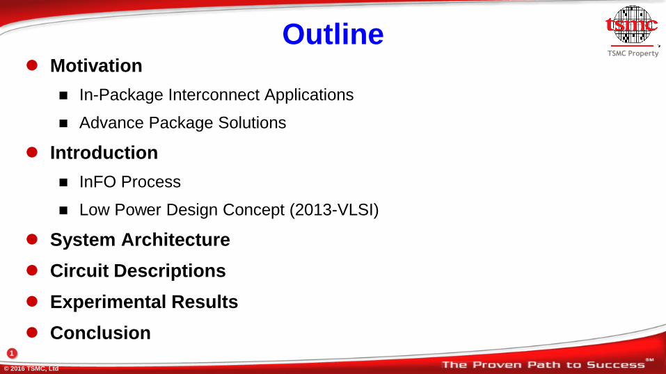
Outline Motivation
In-Package Interconnect Applications
Advance Package Solutions
Introduction
InFO Process
Low Power Design Concept (2013-VLSI)
System Architecture
Circuit Descriptions
Experimental Results
Conclusion
Security C –
TSMC Secret
© 2016 TSMC, Ltd
2
TSMC Property
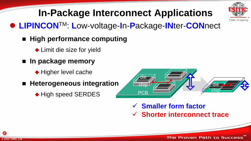
In-Package Interconnect Applications
High performance computing
Limit die size for yield
In package memory
Higher level cache
Heterogeneous integration
High speed SERDES
LIPINCONTM: Low-voltage-In-Package-INter-CONnect
Smaller form factor
Shorter interconnect trace
die
chip
PCB
die chip

Security C –
TSMC Secret
© 2016 TSMC, Ltd
3
TSMC Property
High Performance Computing (HPC)
Yield goes down exponentially as die size gets large
Building large dice is quite difficult and very costly
[1] Intel, 2015-ISSCC, “The Xeon Processor..”
~30mm
~20
mm
~15mm
~5m
m
CORE
CORE
CORE
CORE
CORE
CORE
CORE
CORE
CORE
CORE
CORE
CORE
CORE
CORE
CORE
CORE
CORE
CORE

Security C –
TSMC Secret
© 2016 TSMC, Ltd
4
TSMC Property
In Package Memory (IPM) Additional memory hierarchy between
on-chip SRAM and off-chip DDR
Smaller capacity; higher bandwidth;
faster latency
Advantages
DRAM is more cost-effective than
eDRAM
Non-TSV allows fine pitch RDL and
shorten trace between AP and IPM
Short trace enable termination-less IO
design Save main DRAM bandwidth by 60%
[2] Google, 2015-VLSI, “System Challenges..”
Security C –
TSMC Secret
© 2016 TSMC, Ltd
5
TSMC Property
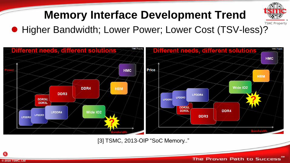
Memory Interface Development Trend
Higher Bandwidth; Lower Power; Lower Cost (TSV-less)?
[3] TSMC, 2013-OIP “SoC Memory..”
?
?
Security C –
TSMC Secret
© 2016 TSMC, Ltd
6
TSMC Property
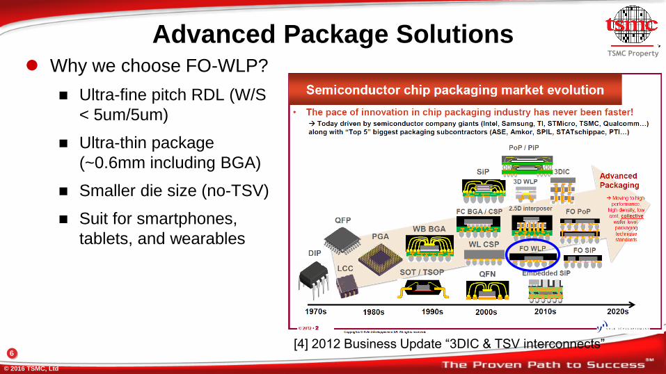
Advanced Package Solutions Why we choose FO-WLP?
Ultra-fine pitch RDL (W/S
< 5um/5um)
Ultra-thin package
(~0.6mm including BGA)
Smaller die size (no-TSV)
Suit for smartphones,
tablets, and wearables
[4] 2012 Business Update “3DIC & TSV interconnects”

Security C –
TSMC Secret
© 2016 TSMC, Ltd
7
TSMC Property
TSMC Package Solution
InFO-WLP (INtegrated Fan-Out Wafer-Level-Package) vs FC-BGA
[5] TSMC, 2012-IEDM, “High-Performance..”
More pin counts with smaller
die size
Lower parasitic resistance
(thicker copper traces)
Lower substrate loss (molding
compound)
Better thermal behavior
(smaller form factor)
Security C –
TSMC Secret
© 2016 TSMC, Ltd
8
TSMC Property
Project Target
Demonstrate an in-package interconnect for in-package
memory in InFO package
Less capable of memory process is considered
Low-Power Low-Latency Small Area
Try to be transparent as possible
2Gbit/s/pin; 64Gbyte/s total bandwidth
Power efficient IO
Prompt and automatic timing-calibration scheme

Security C –
TSMC Secret
© 2016 TSMC, Ltd
9
TSMC Property
D2P Bump : Die-to-Probe Bump
D2D Bump : Die-to-Die Bump
SubstrateSOC
SubstrateMEM
RDL-1/RDL-2/RDL-3RDL-3
UBM
BGA ball
UBM
BGA ball
RDL-3
D2P Bump
BGA BallD2D Bump
InFO Trace
Molding
Compound
Introduction
TSMC InFO side-by-side
560um thickness of packaged chip including 3*RDL & BGA
Height:
~560um

Security C –
TSMC Secret
© 2016 TSMC, Ltd
10
TSMC Property
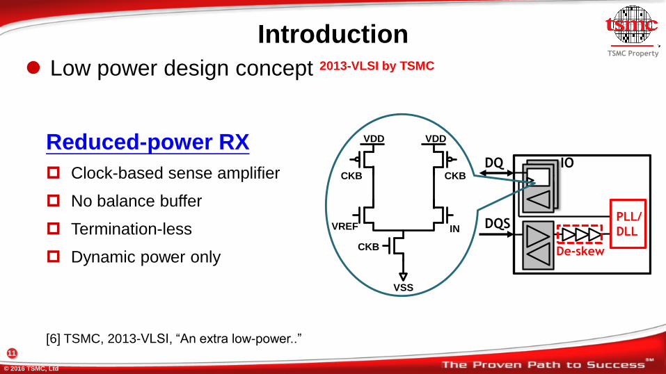
Introduction
Low power design concept 2013-VLSI by TSMC
[6] TSMC, 2013-VLSI, “An extra low-power..”
[7] JESD8-28
VDDQ
PAD VDDQ=0.3V
VSSQ
VSSQ
Reduced-power TX
Low swing with lower VDDQ
Termination-less
Dynamic power only
Security C –
TSMC Secret
© 2016 TSMC, Ltd
11
TSMC Property
Introduction
Low power design concept 2013-VLSI by TSMC
DQ
DQS
De-skew
IO
PLL/
DLL
VDDVDD
CKB CKB
CKB
VSS
VREF IN
Reduced-power RX
Clock-based sense amplifier
No balance buffer
Termination-less
Dynamic power only
[6] TSMC, 2013-VLSI, “An extra low-power..”

Security C –
TSMC Secret
© 2016 TSMC, Ltd
12
TSMC Property
Introduction
Low power design concept 2013-VLSI by TSMC
Simplified design in DRAM
Get rid of DLL/PLL in DRAM
DQ
DQS
De-skew
IO
90/270
0/180
DLL
PLLDCDL
SOC Memory
[6] TSMC, 2013-VLSI, “An extra low-power..”
Security C –
TSMC Secret
© 2016 TSMC, Ltd
13
TSMC Property
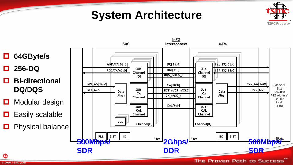
System Architecture
64GByte/s
256-DQ
Bi-directional
DQ/DQS
Modular design
Easily scalable
Physical balance
DLLDLL
SUB-
ChannelSUB-
ChannelSUB-
Channel
SUB-
Channel
[0]
SUB-
CA
Channel
SUB-
CAL
Channel
DQ[15:0]
DQS_t/DQS_c
DMI[1:0]
CA[10:0]
CK_t/CK_c
RST_n/CS_n/CKE
CAL[9:0]
DLLChannel[0]
InFO
Interconnect
PLL
WRDATA[63:0]
RDDATA[63:0]
Slice
Data
Align
DFI_CA[43:0]
DFI_CLK
SUB-
ChannelSUB-
ChannelSUB-
Channel
SUB-
Channel
[0]
SUB-
CA
Channel
SUB-
CAL
Channel
Channel[0]
Slice
Data
Align
P2L_DQ[63:0]
L2P_DQ[63:0]
P2L_CA[43:0]
P2L_CK
SOC MEM
BIST IIC BISTIICSRAM
(Memory
Size
524288=
512 address*
64 bit*
4 cell*
4 ch)
2Gbps/
DDR
500Mbps/
SDR
500Mbps/
SDR
Security C –
TSMC Secret
© 2016 TSMC, Ltd
14
TSMC Property
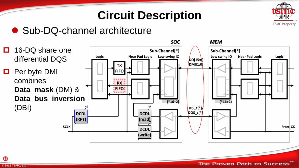
Circuit Description
Sub-DQ-channel architecture
Sub-Channel[*]
DCDL(read)
(*16+2)
SOC
Low swing IO
(*16+2)
DQS_t[*]/DQS_c[*]
Sub-Channel[*]
MEM
DQ[15:0]DMI[1:0]
DCDL(RPT)
DCDL(write)
TXFIFO
Near Pad LogicLogic
RXFIFO
Near Pad Logic
From CK
Low swing IO Logic
SCLK
16-DQ share one
differential DQS
Per byte DMI
combines
Data_mask (DM) &
Data_bus_inversion
(DBI)

Security C –
TSMC Secret
© 2016 TSMC, Ltd
15
TSMC Property
Circuit Description
Sub-DQ-channel architecture
Sub-Channel[*]
DCDL(read)
(*16+2)
SOC
Low swing IO
(*16+2)
DQS_t[*]/DQS_c[*]
Sub-Channel[*]
MEM
DQ[15:0]DMI[1:0]
DCDL(RPT)
DCDL(write)
TXFIFO
Near Pad LogicLogic
RXFIFO
Near Pad Logic
From CK
Low swing IO Logic
SCLK
De-skew
Shift 270o
[6] TSMC, 2013-VLSI, “An extra low-power..”
WRITE-path
DLL-TX [6]

Security C –
TSMC Secret
© 2016 TSMC, Ltd
16
TSMC Property
Circuit Description
Sub-DQ-channel architecture
Sub-Channel[*]
DCDL(read)
(*16+2)
SOC
Low swing IO
(*16+2)
DQS_t[*]/DQS_c[*]
Sub-Channel[*]
MEM
DQ[15:0]DMI[1:0]
DCDL(RPT)
DCDL(write)
TXFIFO
Near Pad LogicLogic
RXFIFO
Near Pad Logic
From CK
Low swing IO Logic
SCLK
READ-path
DLL-RX [6]
RXFIFO
DLL-RPT
Asynchronous
clock between
SCLK & RDQS Shift 270o
De-skew
[6] TSMC, 2013-VLSI, “An extra low-power..”
Security C –
TSMC Secret
© 2016 TSMC, Ltd
17
TSMC Property
Circuit Description
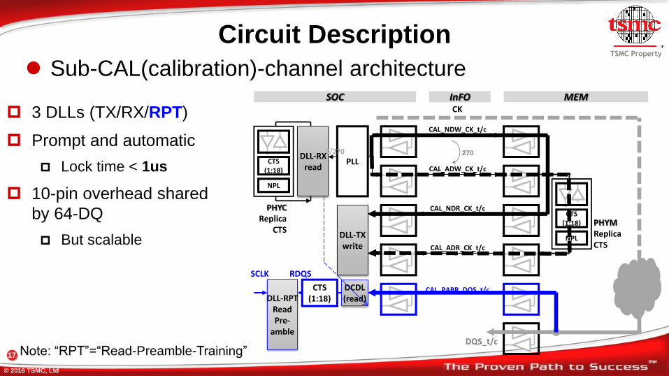
Sub-CAL(calibration)-channel architecture
DCDL(read)
PLL
DLL-TXwrite
CAL_NDR_CK_t/c
CAL_NDW_CK_t/c
CAL_ADW_CK_t/c
CAL_ADR_CK_t/c
PHYMReplicaCTS
CTS(1:18)
NPL
PHYCReplica
CTS
CTS(1:18)
NPL
DLL-RXread
0/270
SOC MEMInFO
CAL_PABR_DQS_t/c
CK
DQS_t/c
DLL-RPTReadPre-
amble
CTS(1:18)
SCLK
270
RDQS
3 DLLs (TX/RX/RPT)
Prompt and automatic
Lock time < 1us
10-pin overhead shared
by 64-DQ
But scalable
Note: “RPT”=“Read-Preamble-Training”

Security C –
TSMC Secret
© 2016 TSMC, Ltd
18
TSMC Property
Latency-cost Degrades System Efficiency
DLLDLL
SUB-
ChannelSUB-
ChannelSUB-
Channel
SUB-
Channel
[0]
SUB-
CA
Channel
SUB-
CAL
Channel
DQ[15:0]
DQS_t/DQS_c
DMI[1:0]
CA[10:0]
CK_t/CK_c
RST_n/CS_n/CKE
CAL[9:0]
DLLChannel[0]
InFO
Interconnect
PLL
WRDATA[63:0]
RDDATA[63:0]
Slice
Data
Align
DFI_CA[43:0]
DFI_CLK
SUB-
ChannelSUB-
ChannelSUB-
Channel
SUB-
Channel
[0]
SUB-
CA
Channel
SUB-
CAL
Channel
Channel[0]
Slice
Data
Align
P2L_DQ[63:0]
L2P_DQ[63:0]
P2L_CA[43:0]
P2L_CK
SOC MEM
BIST IIC BISTIICSRAM
(Memory
Size
524288=
512 address*
64 bit*
4 cell*
4 ch)
4.75T 1.5T
1.875T 2T
(1T=500MHz)
De-/Serialization
ratio: 4
DBI enable
(data-bus-inversion)

Security C –
TSMC Secret
© 2016 TSMC, Ltd
19
TSMC Property
Temperature Drift Monitoring Scheme
PWRRamp
Reset
~PD_PHYC
DLL_LDLOCK_CODE
DLL BGRe-Check
BG_CODE
DLL Lock
DLL BGRe-Check Done
1. Periodic check (1ms )2. Exit Power Gating to IDLE
Compare LOCK_CODE,
BG_CODE
Error > threshold , Raise Error
Error <threshold
MC
Issue PHYC Reset
Temperature drift
Timing variation
Performance degradation
Leveraging DLL architecture
Periodic check (1ms) in background
Alert issue if drift exceed the tolerance
Security C –
TSMC Secret
© 2016 TSMC, Ltd
20
TSMC Property
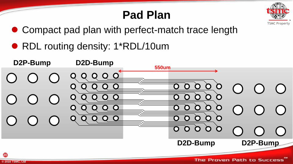
Pad Plan
Compact pad plan with perfect-match trace length
RDL routing density: 1*RDL/10um
550umD2D-Bump D2P-Bump
D2D-Bump D2P-Bump

Security C –
TSMC Secret
© 2016 TSMC, Ltd
21
TSMC Property
Boundary Scan Strategy KGD (Known-Good-Die) – Contactless IO
Compatible with IEEE1149.1
Each die builds in self TAP controller
Support contactless LIPINCON-IO open/short test individually
: InFO Die-to-Probe PAD (Contactable)
: InFO Die-to-Die PAD (Contactless)
Core
…...
InFO D2P PAD
TAP
Boundary Scan Cell
…...
InFO D2D PAD
SubstrateSOC
SubstrateMEM
RDL-1/RDL-2/RDL-3RDL-3
UBM
BGA ball
UBM
BGA ball
RDL-3
Molding
Compound
D2D BumpD2D BumpD2P Bump D2P Bump
Security C –
TSMC Secret
© 2016 TSMC, Ltd
22
TSMC Property
SubstrateSOC
SubstrateMEM
RDL-1/RDL-2/RDL-3RDL-3
UBM
BGA ball
UBM
BGA ball
RDL-3
Molding
Compound
D2D BumpD2D BumpD2P Bump D2P Bump
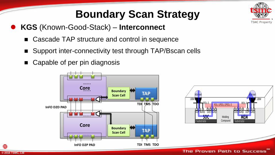
Boundary Scan Strategy KGS (Known-Good-Stack) – Interconnect
Cascade TAP structure and control in sequence
Support inter-connectivity test through TAP/Bscan cells
Capable of per pin diagnosis
Core
…...
InFO D2P PAD
TAPBoundary Scan Cell
…...
InFO D2D PAD
Core…...TAP
Boundary Scan Cell
…...
TDI TMS TDO
TDI TMS TDO

Security C –
TSMC Secret
© 2016 TSMC, Ltd
23
TSMC Property
Packaged-Die Photo After InFO
Fan-out to get the required direct-access BGA balls
SOC
Top-die
(16FF)
MEM
Top-die
(16FF)
[BGA ball side] [7mm*7mm]

Security C –
TSMC Secret
© 2016 TSMC, Ltd
24
TSMC Property
Logic VDD Target=0.8V
Freq. Target=2Gbps
Freq. Max=2.8Gbps
@ VDD=0.8V
VDD -10%
Freq +10%
KGD Shmoo Plot
SOC/MEM-PHY loopback BIST (Logic VDD vs. Frequency)
VDDQ=0.3V
256-DQ toggle
DBI enable
PRBS
+40% Speed

Security C –
TSMC Secret
© 2016 TSMC, Ltd
25
TSMC Property
KGS Shmoo Plot
SOC-to-MEM Write/Read BIST (Logic VDD vs. Frequency)
VDDQ=0.3V
256-DQ toggle
DBI enable
PRBS
Logic VDD Target = 0.8V
Freq. Target=2Gbps
Freq. Max=2.8Gbps
Freq. Max=3.6Gbps
@ VDD=1.0V
VDD -10%
Freq +10%Same speed as KGD

Security C –
TSMC Secret
© 2016 TSMC, Ltd
26
TSMC Property
KGS Shmoo Plot
SOC-to-MEM Write/Read BIST (IO-VDDQ vs. Frequency)
VDD=0.8V
256-DQ toggle
DBI enable
PRBS
IO VDDQ Target=0.3V
Freq. Target=2Gbps
Freq. Max=2.8Gbps
Max Speed
Limited by Logic V
IO VDDQ Min.=0.15V
-50% VDDQ
(150mV)
-50% VDDQ

Security C –
TSMC Secret
© 2016 TSMC, Ltd
27
TSMC Property
Capable of Eye-ploting
0.3V Swing is critical to SSO under wide bus application
How to ensure signal integrity on the un-probed interconnect IO?
X-axis: DCDL
code (7ps)
Y-axis: VREF
code (9.5mV)
VDD=0.8V
256-DQ toggle
DBI enable
PRBS
[VR
EF C
od
e]
[DCDL Code]
0.04V(Noise Ground)
0.15V
0.3V
0V
Org. Capture
Adjusted Capture
Eye Height (225mV)
Eye Width (420ps~0.84UI)

Security C –
TSMC Secret
© 2016 TSMC, Ltd
28
TSMC Property
50.7%
24.9%
14.5%
9.2%
0.8%
Power Breakdown
Digital (0.8V)
LIPINCON-IO (0.8V/0.3V)
DCDL (0.8V)
NPL (0.8V)
Replica cell (0.8V)
Power Breakdown Base on simulation results with 100% toggling conditions
LIPINCON-IO power efficiency:
0.062pJ/bit (consider one single-end IO)
LIPINCON-PHY power efficiency:
0.424pJ/bit
BlocksPower
Consumption
Power
EfficiencyPercentage
Digital (0.8V) 110.00 0.215 50.7%
LIPINCON-IO (0.8V/0.3V) 53.97 0.105 24.9%
DCDL (0.8V) 31.52 0.062 14.5%
NPL (0.8V) 20.00 0.039 9.2%
Replica cell (0.8V) 1.65 0.003 0.8%
SUM 217.141 0.424 100.0%
(mW) (mW/Gb/s)
Security C –
TSMC Secret
© 2016 TSMC, Ltd
29
TSMC Property
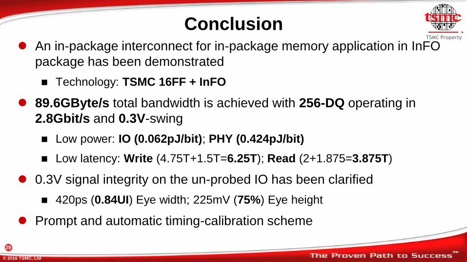
Conclusion An in-package interconnect for in-package memory application in InFO
package has been demonstrated
Technology: TSMC 16FF + InFO
89.6GByte/s total bandwidth is achieved with 256-DQ operating in
2.8Gbit/s and 0.3V-swing
Low power: IO (0.062pJ/bit); PHY (0.424pJ/bit)
Low latency: Write (4.75T+1.5T=6.25T); Read (2+1.875=3.875T)
0.3V signal integrity on the un-probed IO has been clarified
420ps (0.84UI) Eye width; 225mV (75%) Eye height
Prompt and automatic timing-calibration scheme
Security C –
TSMC Secret
© 2016 TSMC, Ltd
30
TSMC Property
Acknowledgement
The authors would like to thank TSMC “InFO-IP” team for InFO
back-end support, TSMC “IPPM” team for measurement support,
and “System-BD” team for business help.
The authors would also like to specially thank “Mentor Graphics”
for boundary scan design collaboration.
Security C –
TSMC Secret
© 2016 TSMC, Ltd
31
TSMC Property
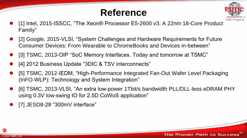
Reference [1] Intel, 2015-ISSCC, “The Xeon® Processor E5-2600 v3: A 22nm 18-Core Product
Family”
[2] Google, 2015-VLSI, “System Challenges and Hardware Requirements for Future
Consumer Devices: From Wearable to ChromeBooks and Devices in-between”
[3] TSMC, 2013-OIP “SoC Memory Interfaces. Today and tomorrow at TSMC”
[4] 2012 Business Update “3DIC & TSV interconnects”
[5] TSMC, 2012-IEDM, “High-Performance Integrated Fan-Out Wafer Level Packaging
(InFO-WLP): Technology and System Integration”
[6] TSMC, 2013-VLSI, “An extra low-power 1Tbit/s bandwidth PLL/DLL-less eDRAM PHY
using 0.3V low-swing IO for 2.5D CoWoS application”
[7] JESD8-28 “300mV interface”


![1 Taiwan International Fastener Show [Profile] Taiwan External Trade Develop Council (TAITRA) Taiwan Industrial Fasteners Institute](https://img.pdfslide.us/doc/110x75/56649d185503460f949eda3e/1-taiwan-international-fastener-show-profile-wwwfastenertaiwancom-taiwan.jpg)