Embed Size (px)
Citation preview
Process Variation Immunity of Alternative 16nmHK/MG-based FPGA Logic Blocks
Ahmad Alzahrani and Ronald F. DeMaraDepartment of Electrical Engineering and Computer Science
University of Central Florida, Orlando, FL 32816-2362Email:{azahrani@knights, demara@mail}.ucf.edu, http://cal.ucf.edu*
Abstract—Continued miniaturization of semiconductor tech-nology to nanoscale dimensions has elevated reliability challengesof high density Field-Programmable Gate Arrays (FPGA) devicesdue to increasing impacts of Process Variation (PV). The issueis addressed herein using a systematic bottom-up analysis bydetermining the relative influence of PV on alternate designrealizations of FPGA logic blocks. Results for conventional designstructures are obtained through detailed SPICE simulations andrelated to structural risk features. Namely, Transmission Gate(TG) and Pass Transistor (PT) based MUX architectures forrealizing Look-Up-Tables (LUTs) are compared. At thresholdvoltage variation σVth = 14%, PT-based designs that meetthe 95% yield objective can exhibit as high delay variation as23.3%. PV impact can be reduced to 4.9% if TG-based LUT isconsidered. Finally, the impact of transistor sizing is investigatedas a method of mitigating PV susceptibility in FPGA structures.
I. INTRODUCTION
Advancement of CMOS manufacturing technology to re-duce device dimensions has ushered in significant challengesresulting from Process Variation (PV) [1]. Significant sourcesof variation in sub-45nm manufacturing processes includeimprecise lithography, etching, deposition, and dopant im-plantation [2]. These can lead to Random Dopant Fluctu-ation, Line-Edge Roughness, and structure dimension vari-ance, e.g. channel length and oxide thickness. Variation inthese physical parameters translates into deviation in deviceelectric characteristics, such as Vth and drive current Idsat,from the intended specifications. Therefore, PV can lead toslow, weak, or defective transistors, thus affecting yield, finalproduct performance, efficiency, and reliability. The Interna-tional Technology Roadmap for Semiconductors (ITRS) hasestimated that Vth variation, given by three-sigma (3σVth
),has already reached 42% (σVth
= 14%) and can reach upto 79% (σVth
= 26%) for near-future process technology,according to table DESN10 in [3]. Fortunately, PV exhibitsa statistical nature which makes it feasible to study at variouslevels of design abstraction, which are compared in this paperfor alternate functional realizations. Traditionally, StatisticalStatic Timing Analysis (SSTA) technique is used to predictdesign behavior at design-time and accordingly devise theappropriate mitigation strategies to minimize PV effects andincrease yield.
SRAM-based Field Programmable Gate Arrays (FPGAs)have been at the frontier of technology scaling owing tothe increased demand for high performance and low-powerreconfigurable systems. Thus, the design of FPGA logic blockshave an increasing need to cope with PV issues emerging ateach new process node. Contemporary SRAM-based FPGAs
* This work is supported by the Ministry of Higher Education of SaudiArabia under scholarship grant SACM64923.
designs are composed of array of tiles, which contain LogicClusters (LCs), Connection Boxes (CBs), and Switching Box(SBs). A logic cluster contains Look-Up-Tables (LUTs) andflip-flops which implement logic functionality. Connectionand switching boxes provide the required connectivity amongLCs and routing channels. Commercial FPGAs have utilizedmultiplexers (MUXes) to implement LUTs, CBs, and SBs dueto the lower required number of control inputs and favorablearea-delay product [4][5]. Because of the uniform fabric ofmodern SRAM-based FPGAs, multiplexers can be viewedas a dominating fundamental logic structure in these devicesbesides SRAM cells. To reduce cost and area, FPGA vendorshave relied on NMOS Pass-Transistors (PTs) as the preferredfundamental switching elements for realizing multiplexers.NMOS PTs are known for conveying a weak high logic signallevel at a saturated output of VDD−Vth. As aggressive scalingof devices continues, the voltage difference between VDD andVth decreases; thus half-latch restoration logic has been used tomitigate resultant reliability and performance issues. Recently,the work in [4] investigated the use of Transmission Gates(TGs) as an alternative design option to implement FPGAsblocks while achieving lower area-delay product. In [6], PV-induced failure rate in a PT-based multiplexer without therestoration logic is studied. However, the work did not considerthat transistor sizing can substantially reduce defect rate asdemonstrated later in this work. To the best of our knowledge,there has not been a study on how PT and TG-based structurescompare as design options for FPGA structures under the effectof variations. In this paper, we study the impact of variationon these two design alternatives and report the Defective Rate,Delay, and Energy Delay Product (EDP).
The remainder of the paper is organized as follows. SectionII provides a background on PV and the FPGA structuresto be considered for the evaluation. Section III describesthe evaluation framework and toolset adopted for simulation.Results and Conclusions are discussed in Section IV.
II. EFFECTS OF PROCESS VARIATION
Process variation is a key challenge for continued tech-nology scaling. It can affect functional, leakage, or timingyield and power efficiency of final design due to the need forwider voltage margins. Variation can include any nanoscopicimprecision in manufacturing processes during physical re-alization of design layout. PV can be manifested as Die-to-Die (D2D) or WithIn-Die (WID) variations. WID variationbecomes a significant factor in the impact of variation and thusis the scope of this work. At the individual transistor-level,the prominent negative effect of WID variation is observedas a variation in device threshold voltage and the amountof current flow during transistor ON-OFF states. Threshold
voltage variation σVthis essentially a function of device
dimensions and dopant density in the channel as expressedbelow [7].
σVth∝ toxεox
√nch
3 · w · l(1)
where w and l are the channel width and length respectively,tox is the gate oxide thickness, εox is the permittivity of oxidelayer, and nch is the concentration of channel doping. Sincedevice delay tg is tightly dependent on Vth as given by thewell-cited alpha-power law in (2), high variation can severelyimpact transistor speed and cause timing yield loss.
tg ∝leff · VDD
(VDD − Vth)α(2)
where leff is the effective channel length, α is a constantdepending on process technology. Similarly, threshold voltageaffects the transistor ON saturation current IDsat
as given in(3) which results in a weak or slow driving transistor.
IDsat=w · νsat · εox
tox· (Vgs − Vth − Vdsat
) (3)
where Vgs is the gate voltage, and Vdsatis the saturation
drain voltage. This effect leads to a situation where a transistoris either not a strong enough to trigger downstream gates, ordoes so at a slow pace causing higher sub-threshold currentto flow in fanout gates. Thus, PV can cause a functional yieldloss and power constraint violation even if timing requirementsdetermined by the proportion of gates in the critical pathare met. In this paper, we consider the case where PV cancause FPGA structures to functionally fail. Previous workfor the effects of PV in FPGAs have considered the timingand leakage yield [8] [9], whereas in [6] functional failure isstudied for a single MUX design without considering otherdesign alternatives or device-level mitigation strategies suchas transistor sizing to combat variation. FPGA group testingstudied for hard faults can offer an emerging alternative [10].
The key logic structures for realizing SRAM-based FP-GAs are SRAM cells and MUXes. Due to their ubiquitousapplications, variation in SRAM cells has been extensivelystudied [11]. In the case of FPGAs, the effect of PV on SRAMcells is less limited since SRAM cells are not packed in anarray structure in the same organization used in other customVLSI designs, e.g. cache memory. In addition, SRAM cellsin FPGAs are not often written; thus, the overhead imposedby any deployed technique to avoid PV-induced write failurescan be negligible. To that end, we focus on MUX-basedstructures and consider two commonly accepted design optionsfor implementing them in FPGAs [12]. Namely, the effect ofvariation on PT-based MUXes with half-latches and TG-basedcounterparts are compared.
A. Pass Transistor-based Multiplexers with Half-latch
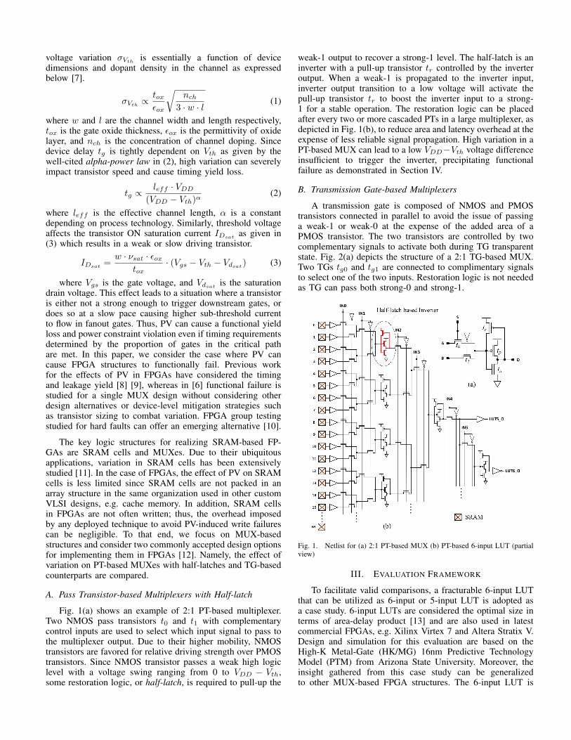
Fig. 1(a) shows an example of 2:1 PT-based multiplexer.Two NMOS pass transistors t0 and t1 with complementarycontrol inputs are used to select which input signal to pass tothe multiplexer output. Due to their higher mobility, NMOStransistors are favored for relative driving strength over PMOStransistors. Since NMOS transistor passes a weak high logiclevel with a voltage swing ranging from 0 to VDD − Vth,some restoration logic, or half-latch, is required to pull-up the
weak-1 output to recover a strong-1 level. The half-latch is aninverter with a pull-up transistor tr controlled by the inverteroutput. When a weak-1 is propagated to the inverter input,inverter output transition to a low voltage will activate thepull-up transistor tr to boost the inverter input to a strong-1 for a stable operation. The restoration logic can be placedafter every two or more cascaded PTs in a large multiplexer, asdepicted in Fig. 1(b), to reduce area and latency overhead at theexpense of less reliable signal propagation. High variation in aPT-based MUX can lead to a low VDD−Vth voltage differenceinsufficient to trigger the inverter, precipitating functionalfailure as demonstrated in Section IV.
B. Transmission Gate-based Multiplexers
A transmission gate is composed of NMOS and PMOStransistors connected in parallel to avoid the issue of passinga weak-1 or weak-0 at the expense of the added area of aPMOS transistor. The two transistors are controlled by twocomplementary signals to activate both during TG transparentstate. Fig. 2(a) depicts the structure of a 2:1 TG-based MUX.Two TGs tg0 and tg1 are connected to complimentary signalsto select one of the two inputs. Restoration logic is not neededas TG can pass both strong-0 and strong-1.
Fig. 1. Netlist for (a) 2:1 PT-based MUX (b) PT-based 6-input LUT (partialview)
III. EVALUATION FRAMEWORK
To facilitate valid comparisons, a fracturable 6-input LUTthat can be utilized as 6-input or 5-input LUT is adopted asa case study. 6-input LUTs are considered the optimal size interms of area-delay product [13] and are also used in latestcommercial FPGAs, e.g. Xilinx Virtex 7 and Altera Stratix V.Design and simulation for this evaluation are based on theHigh-K Metal-Gate (HK/MG) 16nm Predictive TechnologyModel (PTM) from Arizona State University. Moreover, theinsight gathered from this case study can be generalizedto other MUX-based FPGA structures. The 6-input LUT is
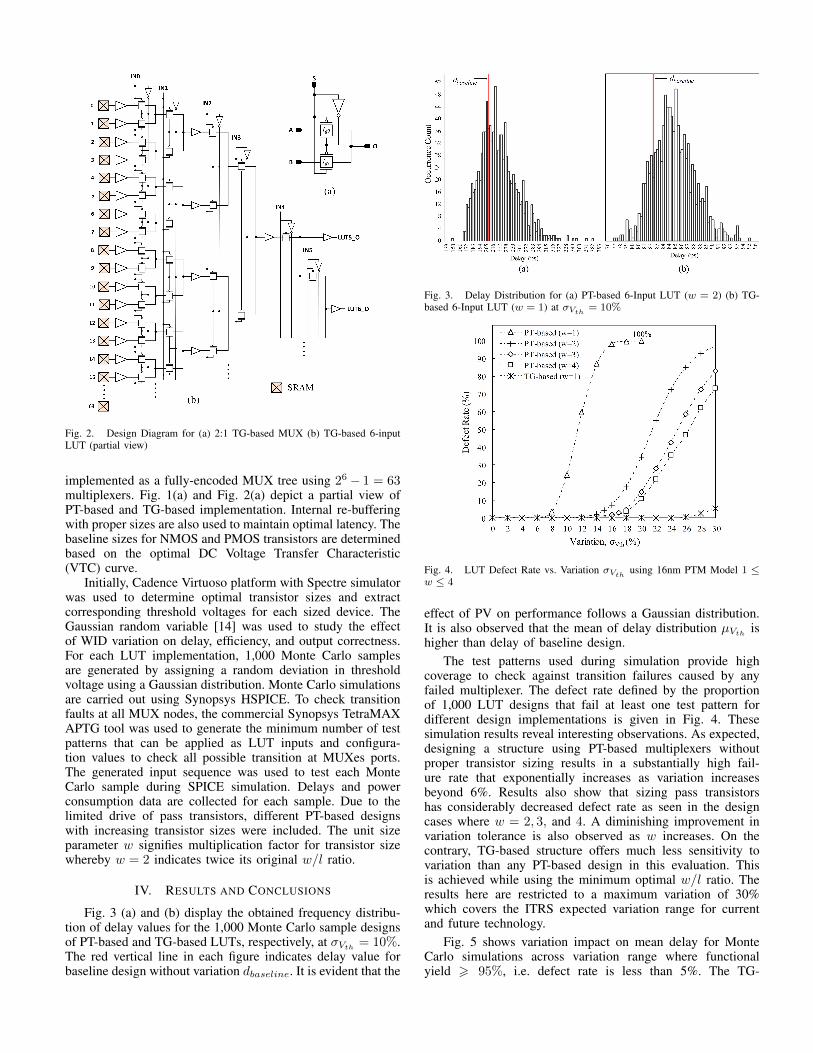
Fig. 2. Design Diagram for (a) 2:1 TG-based MUX (b) TG-based 6-inputLUT (partial view)
implemented as a fully-encoded MUX tree using 26 − 1 = 63multiplexers. Fig. 1(a) and Fig. 2(a) depict a partial view ofPT-based and TG-based implementation. Internal re-bufferingwith proper sizes are also used to maintain optimal latency. Thebaseline sizes for NMOS and PMOS transistors are determinedbased on the optimal DC Voltage Transfer Characteristic(VTC) curve.
Initially, Cadence Virtuoso platform with Spectre simulatorwas used to determine optimal transistor sizes and extractcorresponding threshold voltages for each sized device. TheGaussian random variable [14] was used to study the effectof WID variation on delay, efficiency, and output correctness.For each LUT implementation, 1,000 Monte Carlo samplesare generated by assigning a random deviation in thresholdvoltage using a Gaussian distribution. Monte Carlo simulationsare carried out using Synopsys HSPICE. To check transitionfaults at all MUX nodes, the commercial Synopsys TetraMAXAPTG tool was used to generate the minimum number of testpatterns that can be applied as LUT inputs and configura-tion values to check all possible transition at MUXes ports.The generated input sequence was used to test each MonteCarlo sample during SPICE simulation. Delays and powerconsumption data are collected for each sample. Due to thelimited drive of pass transistors, different PT-based designswith increasing transistor sizes were included. The unit sizeparameter w signifies multiplication factor for transistor sizewhereby w = 2 indicates twice its original w/l ratio.
IV. RESULTS AND CONCLUSIONS
Fig. 3 (a) and (b) display the obtained frequency distribu-tion of delay values for the 1,000 Monte Carlo sample designsof PT-based and TG-based LUTs, respectively, at σVth
= 10%.The red vertical line in each figure indicates delay value forbaseline design without variation dbaseline. It is evident that the
Fig. 3. Delay Distribution for (a) PT-based 6-Input LUT (w = 2) (b) TG-based 6-Input LUT (w = 1) at σVth
= 10%
Fig. 4. LUT Defect Rate vs. Variation σVthusing 16nm PTM Model 1 ≤
w ≤ 4
effect of PV on performance follows a Gaussian distribution.It is also observed that the mean of delay distribution µVth
ishigher than delay of baseline design.
The test patterns used during simulation provide highcoverage to check against transition failures caused by anyfailed multiplexer. The defect rate defined by the proportionof 1,000 LUT designs that fail at least one test pattern fordifferent design implementations is given in Fig. 4. Thesesimulation results reveal interesting observations. As expected,designing a structure using PT-based multiplexers withoutproper transistor sizing results in a substantially high fail-ure rate that exponentially increases as variation increasesbeyond 6%. Results also show that sizing pass transistorshas considerably decreased defect rate as seen in the designcases where w = 2, 3, and 4. A diminishing improvement invariation tolerance is also observed as w increases. On thecontrary, TG-based structure offers much less sensitivity tovariation than any PT-based design in this evaluation. Thisis achieved while using the minimum optimal w/l ratio. Theresults here are restricted to a maximum variation of 30%which covers the ITRS expected variation range for currentand future technology.
Fig. 5 shows variation impact on mean delay for MonteCarlo simulations across variation range where functionalyield > 95%, i.e. defect rate is less than 5%. The TG-
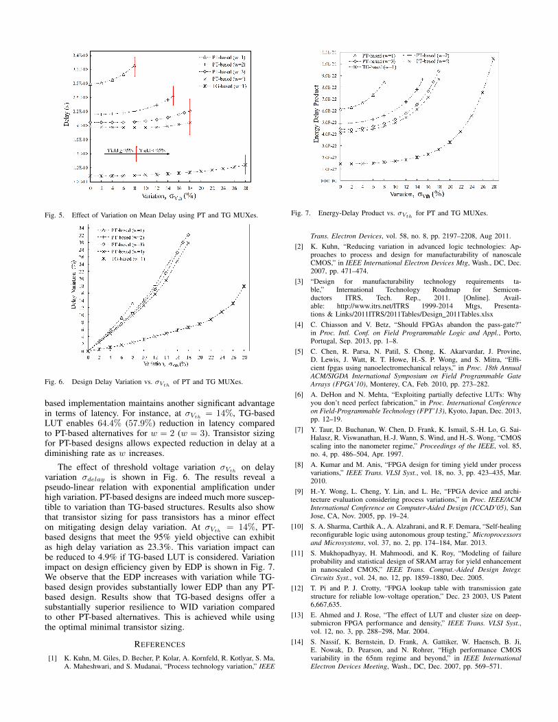
Fig. 5. Effect of Variation on Mean Delay using PT and TG MUXes.
Fig. 6. Design Delay Variation vs. σVthof PT and TG MUXes.
based implementation maintains another significant advantagein terms of latency. For instance, at σVth
= 14%, TG-basedLUT enables 64.4% (57.9%) reduction in latency comparedto PT-based alternatives for w = 2 (w = 3). Transistor sizingfor PT-based designs allows expected reduction in delay at adiminishing rate as w increases.
The effect of threshold voltage variation σVthon delay
variation σdelay is shown in Fig. 6. The results reveal apseudo-linear relation with exponential amplification underhigh variation. PT-based designs are indeed much more suscep-tible to variation than TG-based structures. Results also showthat transistor sizing for pass transistors has a minor effecton mitigating design delay variation. At σVth
= 14%, PT-based designs that meet the 95% yield objective can exhibitas high delay variation as 23.3%. This variation impact canbe reduced to 4.9% if TG-based LUT is considered. Variationimpact on design efficiency given by EDP is shown in Fig. 7.We observe that the EDP increases with variation while TG-based design provides substantially lower EDP than any PT-based design. Results show that TG-based designs offer asubstantially superior resilience to WID variation comparedto other PT-based alternatives. This is achieved while usingthe optimal minimal transistor sizing.
REFERENCES
[1] K. Kuhn, M. Giles, D. Becher, P. Kolar, A. Kornfeld, R. Kotlyar, S. Ma,A. Maheshwari, and S. Mudanai, “Process technology variation,” IEEE
Fig. 7. Energy-Delay Product vs. σVthfor PT and TG MUXes.
Trans. Electron Devices, vol. 58, no. 8, pp. 2197–2208, Aug 2011.[2] K. Kuhn, “Reducing variation in advanced logic technologies: Ap-
proaches to process and design for manufacturability of nanoscaleCMOS,” in IEEE International Electron Devices Mtg, Wash., DC, Dec.2007, pp. 471–474.
[3] “Design for manufacturability technology requirements ta-ble,” International Technology Roadmap for Semicon-ductors ITRS, Tech. Rep., 2011. [Online]. Avail-able: http://www.itrs.net/ITRS 1999-2014 Mtgs, Presenta-tions & Links/2011ITRS/2011Tables/Design 2011Tables.xlsx
[4] C. Chiasson and V. Betz, “Should FPGAs abandon the pass-gate?”in Proc. Intl. Conf. on Field Programmable Logic and Appl., Porto,Portugal, Sep. 2013, pp. 1–8.
[5] C. Chen, R. Parsa, N. Patil, S. Chong, K. Akarvardar, J. Provine,D. Lewis, J. Watt, R. T. Howe, H.-S. P. Wong, and S. Mitra, “Effi-cient fpgas using nanoelectromechanical relays,” in Proc. 18th AnnualACM/SIGDA International Symposium on Field Programmable GateArrays (FPGA’10), Monterey, CA, Feb. 2010, pp. 273–282.
[6] A. DeHon and N. Mehta, “Exploiting partially defective LUTs: Whyyou don’t need perfect fabrication,” in Proc. International Conferenceon Field-Programmable Technology (FPT’13), Kyoto, Japan, Dec. 2013,pp. 12–19.
[7] Y. Taur, D. Buchanan, W. Chen, D. Frank, K. Ismail, S.-H. Lo, G. Sai-Halasz, R. Viswanathan, H.-J. Wann, S. Wind, and H.-S. Wong, “CMOSscaling into the nanometer regime,” Proceedings of the IEEE, vol. 85,no. 4, pp. 486–504, Apr. 1997.
[8] A. Kumar and M. Anis, “FPGA design for timing yield under processvariations,” IEEE Trans. VLSI Syst., vol. 18, no. 3, pp. 423–435, Mar.2010.
[9] H.-Y. Wong, L. Cheng, Y. Lin, and L. He, “FPGA device and archi-tecture evaluation considering process variations,” in Proc. IEEE/ACMInternational Conference on Computer-Aided Design (ICCAD’05), SanJose, CA, Nov. 2005, pp. 19–24.
[10] S. A. Sharma, Carthik A., A. Alzahrani, and R. F. Demara, “Self-healingreconfigurable logic using autonomous group testing,” Microprocessorsand Microsystems, vol. 37, no. 2, pp. 174–184, Mar. 2013.
[11] S. Mukhopadhyay, H. Mahmoodi, and K. Roy, “Modeling of failureprobability and statistical design of SRAM array for yield enhancementin nanoscaled CMOS,” IEEE Trans. Comput.-Aided Design Integr.Circuits Syst., vol. 24, no. 12, pp. 1859–1880, Dec. 2005.
[12] T. Pi and P. J. Crotty, “FPGA lookup table with transmission gatestructure for reliable low-voltage operation,” Dec. 23 2003, US Patent6,667,635.
[13] E. Ahmed and J. Rose, “The effect of LUT and cluster size on deep-submicron FPGA performance and density,” IEEE Trans. VLSI Syst.,vol. 12, no. 3, pp. 288–298, Mar. 2004.
[14] S. Nassif, K. Bernstein, D. Frank, A. Gattiker, W. Haensch, B. Ji,E. Nowak, D. Pearson, and N. Rohrer, “High performance CMOSvariability in the 65nm regime and beyond,” in IEEE InternationalElectron Devices Meeting, Wash., DC, Dec. 2007, pp. 569–571.