Embed Size (px)
Citation preview

A 1280×1024-15µm CTIA ROIC for SWIR FPAs
Selim Eminoglu, Murat Isikhan, Nusret Bayhan, M. Ali Gulden, O. Samet Incedere, S. Tuncer Soyer, Serhat Kocak,
Cem Yalcin, M. Cem B. Ustundag, Ozge Turan, Umut Eksi, and Tayfun Akin
Mikro-Tasarim Ltd., ODTU-Teknokent, Ankara, 06530, TURKEY
ABSTRACT
This paper reports the development of a new SXGA format low-noise CTIA ROIC (MT12815CA-3G) suitable for
mega-pixel SWIR InGaAs detector arrays for low-light imaging applications. MT12815CA-3G is the first mega-pixel
standard ROIC product from Mikro-Tasarim, which is a fabless semiconductor company specialized in the development
of ROICs and ASICs for visible and infrared hybrid imaging sensors. MT12815CA-3G is a low-noise snapshot
mega-pixel CTIA ROIC, has a format of 1280 × 1024 (SXGA) and pixel pitch of 15 µm. MT12815CA-3G has been
developed with the system-on-chip architecture in mind, where all the timing and biasing for this ROIC are generated
on-chip without requiring any special external inputs. MT12815CA-3G is a highly configurable ROIC with many
features that can be programmed through a 3-wire serial interface allowing on-the-fly configuration the ROIC. It
performs snapshot operation both using Integrate-Then-Read (ITR) and Integrate-While-Read (IWR) modes. The CTIA
type pixel input circuitry has 3 gain modes with programmable full-well-capacity (FWC) values of 10K e-, 20K e-, and
350K e- in the very high gain (VHG), high-gain (HG), and low-gain (LG) modes, respectively. MT12815CA-3G has an
input referred noise level of less than 5 e- in the very high gain (VHG) mode, suitable for very low-noise SWIR imaging
applications. MT12815CA-3G has 8 analog video outputs that can be programmed in 8, 4, or 2-output modes with a
selectable analog reference for pseudo-differential operation. The ROIC runs at 10 MHz and supports frame rate values
up to 55 fps in the 8-output mode. The integration time of the ROIC can be programmed up to 1s in steps of 0.1 µs. The
ROIC uses 3.3 V and 1.8V supply voltages and dissipates less than 350 mW in the 4-output mode. MT12815CA-3G is
fabricated using a modern mixed-signal CMOS process on 200 mm CMOS wafers, and there are 44 ROIC parts per
wafer. The probe tests show that the die yield is higher than 70%, which corresponds to more than 30 working ROIC
parts per wafer typically. MT12815CA-3G ROIC is available as tested wafers or dies, where a detailed test report and
wafer map are provided for each wafer. A compact USB 3.0 based test camera and imaging software are also available
for the customers to test and evaluate the imaging performance of SWIR sensors built using MT12815CA-3G ROICs.
Mikro-Tasarim has also recently developed a programmable mixed-signal application specific integrated circuit (ASIC),
called MTAS1410X8, which is designed to perform ROIC driving and digitization functions for ROICs with analog
outputs, such as MT12815CA-3G and MT6415CA ROIC products of Mikro-Tasarim. MTAS1410X8 has 8
simultaneously working 14-bit analog-to-digital converters (ADCs) with integrated programmable gain amplifiers
(PGAs), video input buffers, programmable controller, and high-speed digital video interface supporting various formats
including Camera Link. MT12815CA-3G ROIC together with MTAS1410X8 ASIC can be used to develop low-noise
high-resolution SWIR imaging sensors with low power dissipation and reduced board area for the camera electronics.
Keywords: SWIR, ROIC, CTIA, 1280×1024, MT12815CA-3G, snapshot, low-noise, InGaAs, ASIC, MTAS1410X8
1. INTRODUCTION
Mikro-Tasarim is a fabless IC design company, specialized in the development of Readout Integrated Circuits (ROICs)
and Application Specific Integrated Circuits (ASICs) for hybrid and monolithic infrared Focal Plane Arrays (FPAs)
working in the SWIR, MWIR, and LWIR optical bands [1-6]. Hybrid FPAs are built using a two-chip solution
composed of a ROIC and photodiode detector array (PDA). The PDA is fabricated using detector materials with low
band gap energy levels to be able to detect low energy infrared photons. Hybrid infrared FPAs typically require
cryogenic operation down to liquid nitrogen temperature (77K) or lower to be able to reduce the thermally generated
dark current in the detector pixels. The PDAs used for the hybrid infrared FPAs are built using various detector
materials such as InGaAs, InSb, HgCdTe, QWIP, and Type-II Super Lattice (T2SL).
Infrared Technology and Applications XLI, edited by Bjørn F. Andresen, Gabor F. Fulop, Charles M. Hanson, Paul R. Norton, Proc. of SPIE Vol. 9451,
94510W · © 2015 SPIE · CCC code: 0277-786X/15/$18 · doi: 10.1117/12.2179537
Proc. of SPIE Vol. 9451 94510W-1
Downloaded From: http://proceedings.spiedigitallibrary.org/ on 10/03/2015 Terms of Use: http://spiedigitallibrary.org/ss/TermsOfUse.aspx

I Il G
The spectral bands of the hybrid infrared FPAs put different requirements for the ROICs in terms of pixel input circuitry
type, Full-Well-Capacity (FWC), and FPA operating temperature, making it necessary to use optimized ROIC products
for different PDAs working in different spectral bands. Table 1 gives the list of the standard ROIC products of
Mikro-Tasarim developed for various infrared FPAs working in the SWIR, MWIR, and LWIR bands [6].
Mikro-Tasarim provides standard ROIC products for hybrid infrared FPAs built using various detector types with wide
range of input circuitry selections (SF: Source Follower, DI: Direct-Injection, and CTIA: Capacitive Trans-Impedance
Amplifier), with different FWC values, and capable of operating from room temperature down to cryogenic
temperatures. Mikro-Tasarim also offers standard ROICs for uncooled microbolometer FPAs with resistive pixel arrays,
which are fabricated monolithically at wafer level using MEMS based surface micro-machining techniques [3-4].
Mikro-Tasarim recently announced a product line composed of ASICs, which are developed to drive and digitize analog
ROIC products to simplify the system integration and enable the development of high performance camera cores with
reduced size and power dissipation. Mikro-Tasarim has recently been focused on the development of ROICs and ASICs
for uncooled infrared FPAs, such hybrid SWIR imaging sensors using InGaAs detector arrays and monolithic LWIR
imaging sensors using microbolometer detector arrays. One common property for these FPA types is that they are
operated at room temperature, are small in size, have relatively lower cost compared to their cooled alternatives, and
therefore have a great potential for high volume commercial and industrial applications.
Table 1. Standard ROIC products of Mikro-Tasarim developed for various infrared FPAs [6].
Product MT6425DA MT6425CA MT6415CA MT12815CA-3G MT3825BA MT1625BA
Die Photo
FPA Format 640×512 640×512 640×512 1280×1024 384×288 160×120
Pixel Pitch 25µm 25µm 15µm 15µm 25µm 25µm
Input Type DI CTIA CTIA CTIA µBolometer µBolometer
PDA Type InSb, HgCdTe,
QWIP, T2SL
InGaAs,
HgCdTe
InGaAs,
HgCdTe
InGaAs,
HgCdTe
VOx VOx
Spectral
Band
MWIR, LWIR SWIR SWIR SWIR LWIR LWIR
SWIR FPAs using InGaAs detector arrays gained considerable attention over the last years due to unique advantages of
both SWIR optical band and mature InGaAs FPA technology [7-11]. It is relatively easier for the viewers to understand
SWIR images as they look similar to the visible images, since both type of images are formed by capturing the reflected
light from the ambient rather than the radiated light common for MWIR and LWIR bands. In addition, SWIR light can
pass through regular glass, allowing the use of lower cost optics [8]. Furthermore, the dark current values in the InGaAs
FPAs have been decreased considerably over the last years, which allows building compact and low-power uncooled
SWIR cameras [9]. Finally, due to shorter wavelengths involved in SWIR imaging, potentially much smaller pixels, and
therefore, more compact and higher resolution SWIR FPAs can be built without being limited by the optical diffraction
phenomena [12], at least for practical pixel sizes that can be hybridized with the flip-chip technique. Furthermore, there
are some efforts to fabricate very low-cost SWIR sensors using colloidal quantum dots deposited and patterned
monolithically over the ROICs at wafer level [13]. This new monolithic technology, at the expense of reduced
sensitivity, can potentially reduce the manufacturing cost of the SWIR FPAs drastically, compared to the conventional
InGaAs or HgCdTe based SWIR FPA fabrication technologies utilizing flip-chip technique at individual die level.
Proc. of SPIE Vol. 9451 94510W-2
Downloaded From: http://proceedings.spiedigitallibrary.org/ on 10/03/2015 Terms of Use: http://spiedigitallibrary.org/ss/TermsOfUse.aspx

Mikro-Tasarim offers three CTIA ROICs as standard products, which have system-on-chip architecture with snapshot
operation capability, where all the required timing, biasing, and configuration are done using on-chip circuitry without
requiring any critical external inputs. MT6425CA is the first standard CTIA ROIC product of Mikro-Tasarim, and has a
format of 640×512 and pixel pitch of 25µm [1]. It has a full-well capacity of 320K electrons and input noise level of
110 e- rms. MT6415CA is the second standard CTIA ROIC of Mikro-Tasarim, which has a format of 640×512 and
pixel pitch of 15µm [2]. MT6415CA has 3 programmable gain settings of very-high-gain (VHG), high-gain (HG) and
low-gain (LG), with 10K, 20K, and 350K electrons full-well capacity values, respectively. In the VHG gain mode, the
MT6415CA has an input referred noise level of 5 e- rms in the integrate-then-read (ITR) snapshot readout mode [2].
MT6415CA has already been coupled with InGaAs detector arrays and a very compact camera module has been
developed which measures 32mm×32mm×35mm and weighs less than 45 gr without the optics [5]. Mikro-Tasarim has
also introduced flat surface version of the MT6415CA ROICs for wafer level monolithic fabrication of SWIR FPAs
using colloidal quantum dots, potentially suitable for low-cost high-volume applications.
This paper reports the third standard CTIA ROIC product from Mikro-Tasarim, namely MT12815CA-3G, which is a
CTIA ROIC with snapshot operation having a 1280×1024 format and 15µm pixel pitch, which is developed mainly for
the SWIR InGaAs detector arrays for low-noise and high-resolution imaging applications. MT12815CA-3G has the
same pixel and readout architecture as the MT6415CA, and supports 4 times larger pixel arrays. Similar to MT6415CA,
MT12815CA-3G has also 3 programmable gain settings of very-high-gain (VHG), high-gain (HG) and low-gain (LG),
with 10K, 20K, and 350K e- full-well capacity values, respectively. In the VHG gain mode, the MT12815CA-3G ROIC
has an input referred noise level of 5 e- rms in the integrate-then-read (ITR) snapshot readout mode.
This paper also reports the development of a programmable mixed-signal application specific integrated circuit (ASIC),
called MTAS1410X8, which is designed to perform ROIC driving and digitization functions mainly for the
MT12815CA-3G and MT6415CA ROIC products of Mikro-Tasarim. This ASIC has a configurable system-on-chip
(SoC) architecture, allowing it to be used together with other ROICs with digital control and analog output features.
MTAS1410X8 ASIC integrates all the external circuitry required to drive the analog ROICs and to digitize their analog
video outputs. It has 8 simultaneously sampling 14-bit analog-to-digital converters (ADCs) with integrated
programmable gain amplifiers (PGAs), video input buffers, programmable controller, and high-speed digital video
interface supporting various formats including Camera Link. MT12815CA-3G ROIC together with MTAS1410X8
ASIC can be used to develop low-noise and high-resolution SWIR imaging sensors with low power dissipation and
reduced board area for the camera electronics.
2. ROIC FEATURES
MT12815CA-3G is a low-noise snapshot CTIA ROIC, which has a format of 1280 × 1024 and a pixel pitch of 15 µm. It
has been developed with the system-on-chip architecture in mind, where all the timing and biasing for this ROIC are
generated on-chip without requiring any external inputs. The ROIC has a 1280 × 1024 array of pixel input circuitry
surrounded by a 10 pixel wide detector common ring. On the ROIC, there is an array of pixel pad openings with a
format of 1300 × 1044, a uniform pitch of 15 µm, and a pad opening size of 4 µm × 4 µm. The ROIC has been designed
to interface both p-on-n and n-on-p detector arrays, where the detector bias can be programmed in 0.7 mV steps.
Table 2 summarizes the technical specifications of the MT12815CA-3G ROIC. MT12815CA-3G has various
programmable features, such as detector biasing, full-well-capacity, integration time, readout modes, number of outputs,
window size, scanning direction, readout signal gain and offset, and number of outputs, all of which can be programmed
via a simple 3-wire serial programming interface (SPI). MT12815CA-3G performs snapshot operation using
Integrate-Then-Read (ITR) and Integrate-While-Read (IWR) modes. The CTIA type pixel input circuitry has three
programmable gain settings with selectable Full-Well-Capacity (FWC) values of 10K e-, 20K e-, and 350K e- in the
very high gain (VHG), high-gain (HG), and low-gain (LG) modes, respectively. MT12815CA-3G has an input referred
noise level of less than 5 e- in the VHG mode, suitable for very low-noise SWIR imaging applications.
MT12815CA-3G has 8 analog video outputs that can be programmed in the 8, 4, or 2-output modes with a selectable
analog reference outputs for pseudo-differential operation. MT12815CA-3G has also an optional programmable
reference clock output, which indicates the optimum sampling time for the analog video outputs to achieve proper
settling at the analog ROIC outputs.
Proc. of SPIE Vol. 9451 94510W-3
Downloaded From: http://proceedings.spiedigitallibrary.org/ on 10/03/2015 Terms of Use: http://spiedigitallibrary.org/ss/TermsOfUse.aspx

Table 2. Technical specifications of MT12815CA-3G ROIC
Array Format 1280 × 1024
Pixel Pitch 15 µm
Pixel Pad Openings 4 µm × 4 µm
Detector Common Ring 10 pixel wide ring around the 1280 × 1024 active array
Pixel Input Circuitry Capacitive Trans-impedance Amplifier (CTIA)
Pixel Input Polarity Supports both p-on-n and n-on-p type detector arrays
Full Well Capacity VHG: 10,000 e- HG: 20,000 e- LG: 350,000 e-
Input Referred Read Noise VHG: < 5 e- HG: < 9 e- LG: < 110 e-
Snapshot Readout Modes Integrate-Then-Read (ITR) and Integrate-While-Read (IWR)
Serial Programming Interface Programmable gain, biasing, timing, number of outputs, and configuration
Integration Time Programmable up to 1 s in 100 ns steps
Number of Analog Outputs Programmable as 2, 4, or 8 analog video outputs with 2 selectable references
Output Swing and Gain ≤ 2.0 V with programmable gain and offset
Pixel Data Rate Nominal 10 MHz per output (up to 12.5MHz)
Frame Rate ≤ 55 fps at full frame rate in IWR mode at 10 MHz
Scanning Direction Programmable in horizontal and vertical directions
Windowing Programmable location and size
Sub-Sampling 2:1 Sub-Sampling, 640×512 image at full view with equivalent pitch of 30µm
Detector Biasing On-Chip programmable biasing in 0.7mV steps
Timing and Configuration On-Chip programmable ROIC timing and configuration
Temperature Sensor On-Chip active sensor with 1mV/K sensitivity
Operating Temperature Room Temperature (300K) and Cryogenic (≥ 65K)
Supply Voltages 3.3V (Analog Blocks and Digital I/O) and 1.8V (Digital Core)
Power Dissipation ≤ 350 mW in the 4-output mode
Die Size 21.8 mm × 21.1 mm
Wafer Diameter 200 mm
Die Per Wafer 44 total Typically 30 working after probe tests
The MT12815CA-3G runs at 10 MHz and supports frame rates up to 55 fps in the 8-output mode. The operating
frequency of the ROIC can be increased to 12.5 MHz to support faster scanning rates as high as 70 fps. The integration
time can be programmed up to 1 s in 100 ns steps. The ROIC uses 3.3 V and 1.8 V supply voltages and dissipates less
than 350 mW in the 4-output mode. The system-on-chip (SoC) architecture of MT12815CA-3G makes it suitable for
software controlled imaging applications, where key parameters of the ROIC such as bias, gain, integration time,
window size, and window location can be programmed through a 3-wire Serial Programming Interface (SPI) on-the-fly
between the imaging frames with minimal communication overhead without causing any loss of frames in the
continuous video stream.
MT12815CA-3G is fabricated using a modern mixed-signal CMOS process on 200 mm CMOS wafers. There are 44
parts per wafer, and probe tests show that the die yield is more than 70%, resulting in more than 30 working parts per
wafer on the average. Tested parts are available at wafer or die levels with test reports and wafer maps. Mikro-Tasarim
has also recently introduced flat surface version of the MT12815CA-3G ROICs for wafer level monolithic fabrication of
SWIR FPAs using colloidal quantum dots. A USB 3.0 based compact camera and imaging software are available
allowing quick imaging tests of hybrid sensors built using MT12815CA-3G ROIC product.
Proc. of SPIE Vol. 9451 94510W-4
Downloaded From: http://proceedings.spiedigitallibrary.org/ on 10/03/2015 Terms of Use: http://spiedigitallibrary.org/ss/TermsOfUse.aspx

3. ROIC ARCHITECTURE
Figure 1 shows the simplified architecture of the signal chain used in the MT12815CA-3G ROIC. MT12815CA-3G
ROIC has basically the same architecture as the MT6415CA ROIC [2]. There is a CTIA type pixel input circuitry,
which interfaces the detector pixel and performs current-to-voltage conversion in the pixel. The ROIC operates in the
snapshot mode, where all the pixels are reset and integrated in parallel. The pixel array is then read out in a sequential
manner, where one line of pixels is selected after another by the vertical scanner, also known as row decoder, and signals
from the pixel array are sent to the column readout circuitry for signal conditioning and output multiplexing. The
column readout circuitry is composed of parallel readout columns, each of which contains basically a column amplifier
(CA), a sample-and-hold (S/H) circuit, and a column multiplexer switch. After the pixel signal is amplified by the
column amplifier, the amplified signal is sampled and stored by the sample-and-hold circuit, before it gets multiplexed
via the column switch in a sequential manner at column level controlled by the horizontal scanner, also known as
column decoder. The multiplexed signal is then driven off chip by the output drivers (OD) operating at the pixel output
data rate of the ROIC.
CA S/H OD
Column Amplifier
Sample &Hold
OutputDriver
CTIA Pixel Input
HorizontalScanner
A
VerticalScanner
output
Figure 1. Simplified architecture of the signal chain integrated in MT12815CA-3G ROIC.
Similar to MT6415CA ROIC, required biasing of the analog circuit modules in the MT12815CA-3G ROIC is generated
on-chip by a programmable bias generator, allowing selection of the optimum biasing condition for the detector arrays or
building blocks in the ROIC for a given imaging application in terms of speed and power. Similarly, required timing
signals for the readout modules are generated on-chip by a highly programmable digital control circuit, which controls
basic static and dynamic features such as the timing in the pixel array and column readout as well as general
multiplexing operations performed in the ROIC for various operating modes and configurations. Many of these features
are configurable on-the-fly through a simple 3-wire SPI, and the ones that have an effect on the ROIC operation are
activated only between the frames to assure continuous video streaming without any frame synchronization problems.
Figure 2 (a) and (b) show the digital output synchronization signals generated by MT12815CA-3G to simplify the
interfacing of the ROIC with Camera Link frame grabbers for the ITR and IWR snapshot operation modes, respectively.
For this purpose, MT12815CA-3G generates Frame_Valid, Line_Valid, Data_Valid, and Pixel_Clk signals, which can
be turned off through SPI programming if they are not used. Frame_Valid defines the time during which the frame data
is valid. Line_Valid defines the time during which the line data is valid, and Data_Valid defines the time during which
the pixel data is valid for sampling by the Analog-to-Digital Converters (ADC) driven by the Pixel_Clk. For custom
made systems, it is possible to use only the Data_Valid signal to capture the analog video data from the ROIC, and in
this case, instead of using a dedicated Pixel_Clk output, sampling clock for the ADCs can be driven from the system
clock with some additional delay required for the proper settling at the ROIC outputs. In the ITR case, initial portion of
the frame time is used for pixel integration without any multiplexing activity to avoid any possible noise coupling in the
system due to any switching activities. However, for the IWR case, pixel integration and output multiplexing activities
are carried out in parallel to shorten the frame time and increase frame rate, which is typically used when the frame rate
is more important than the readout noise.
Proc. of SPIE Vol. 9451 94510W-5
Downloaded From: http://proceedings.spiedigitallibrary.org/ on 10/03/2015 Terms of Use: http://spiedigitallibrary.org/ss/TermsOfUse.aspx

Frame Time
Frame Time
(a)
(b)
Figure 2. Digital output synchronization signals generated by MT12815CA-3G to simplify the interfacing of the ROIC with
Camera Link frame grabbers for (a) the ITR and (b) IWR snapshot operation modes.
MT12815CA-3G can run at frame rates up to 55 fps in the IWR mode at full format resolution using the 8-output mode
when operated at its nominal clock frequency of 10 MHz. At its maximum operating frequency of 12.5MHz, it is
possible to increase the frame rate above 70 fps. At 70 fps in the IWR mode, which corresponds to a frame time of
14.3ms, the ROIC can be operated in the 8-output mode such that integration and read operations are performed in
parallel, utilizing the maximum of the available frame time. For the ITR mode, the frame time is mainly the sum of the
integration time and readout time; therefore, frame rate is reduced depending on the integration time setting. For
example, in the ITR mode with 8 outputs using 5 ms integration time, a frame rate as high as 50 fps can be achieved
when the ROIC is operated at its maximum clock frequency of 12.5 MHz. MT12815CA-3G supports windowing and
sub-sampling modes for high frame rate imaging applications. In the windowing mode, a smaller window size can be
selected with user programmable size and location, which will allow faster frames rates especially in the IWR mode due
to the reduced number of total pixels that need to be read out by the ROIC. For example, for a 640 × 512 window size,
the frame rate can be increased up to 200 fps in the IWR mode at 10 MHz nominal system clock and up to 250 fps at
12.5 MHz system clock. It should also be noted that it is also possible to increase the frame rate even further for smaller
window sizes. In windowing mode, only a portion of the full view is imaged with the maximum possible resolution.
However, in some high speed imaging applications, it may be preferable to keep the full view at the expense of reduced
resolution. MT12815CA-3G has a unique 2:1 sub-sampling mode for such applications, where only 1 pixel in every
2 × 2 pixel array is readout in the same full view but with a reduced image size of 640 × 512 pixels with an equivalent
pitch of 30 µm. By doing this, the full view is maintained at a reduced resolution, and in the IWR mode the frame rate is
increased up to 200 fps at 10 MHz, and up to 250 fps at 12.5 MHz. It should be mentioned that on-the-fly configuration
capability of MT12815CA-3G makes it possible to switch between these modes in between frames in real time without
interrupting continuous video streaming. MT12815CA-3G ROIC has similar multiplexing order as the MT6415CA
ROIC. Table 3 shows the pixel output multiplexing order when the MT12815CA-3G is operated in the 8, 4, and
2-output modes. There are 4 analog outputs with a reference on both top and bottom of the ROIC. The top outputs are
named as A, B, C, and D, and bottom outputs are named as E, F, G, and H. Columns are numbered from 0 to 1279 from
the left to the right, where even columns (0, 2, 4, etc.) are multiplexed through the top outputs, and odd columns (1, 3,
5, etc.) are multiplexed through the bottom outputs. The pixels numbered from 0 to 1279 are located next to each other
in a row with a pitch of 15 µm, and for simplicity only the first 64 of them are shown in this table. The order of the
multiplexed analog outputs is arranged in time in such a way that the output values can easily be sampled, digitized, and
directly saved or displayed without the need for any extra frame memory for pixel sorting.
Proc. of SPIE Vol. 9451 94510W-6
Downloaded From: http://proceedings.spiedigitallibrary.org/ on 10/03/2015 Terms of Use: http://spiedigitallibrary.org/ss/TermsOfUse.aspx

,_.--___.._.._........._ f:--'.
Table 3. Pixel output multiplexing order when the MT12815CA-3G ROIC is operated in 8, 4, and 2-output modes.
# Outputs Pixel Output Multiplexing Order
8 A, E 0, 1 8, 9 16, 17 24, 25 32, 33 40, 41 48, 49 56, 57
B, F 2, 3 10, 11 18, 19 26, 27 34, 35 42, 43 50, 51 58, 59
C, G 4, 5 12, 13 20, 21 28, 29 36, 37 44, 45 52, 53 60, 61
D, H 6, 7 14, 15 22, 23 30, 31 38, 39 46, 47 54, 55 62, 63
4 A, E 0, 1 4, 5 8, 9 12, 13 16, 17 20, 21 24, 25 28, 29
B, F 2, 3 6, 7 10, 11 14, 15 18, 19 22, 23 26, 27 30, 31
2 A, E 0, 1 2, 3 4, 5 6, 7 8, 9 10, 11 12, 13 14, 15
Time T0 T1 T2 T3 T4 T5 T6 T7
MT12815CA-3G uses 3.3 V supply voltages for the analog core as well as digital inputs and outputs, and 1.8 V supply
voltage for the digital core. It dissipates only 350 mW at full frame in the 4-output mode at 10 MHz. Figure 3 shows the
die photograph of the MT12815CA-3G ROIC, which measures 21.8 mm × 21.1 mm in a 180 nm mixed-signal CMOS
process. The top block is the analog column readout circuit with output drivers, the block on the top left corner is the
programmable bias generator, and the block on the left is digital control block with serial programming interface. The
array of pixel input circuitry is placed in the center part of the ROIC, and it is read out in parallel by two column readout
circuitries placed symmetrically on the top and bottom of the pixel array. The pixel array is composed of 1280 × 1024
active pixel elements surrounded by a 10-pixel wide detector common ring. The active pixels and detector common ring
are connected to the detector array using the pad openings on the ROIC. There is an array of pad openings on the ROIC
with a format of 1300 × 1044, and with a pad opening size of 4 µm × 4 µm using a uniform pitch of 15 µm. Although
there are 10 pixel wide detector common ring around the 1280 × 1024 active pixels, 1 pixel wide detector common ring
connection is sufficient for the ROIC to operate properly. Furthermore, there are hybridization and packaging alignment
marks on the ROIC. The hybridization alignment marks are placed on the four corners of the pixel array to be used
during the ROIC metallization and flip-chip bonding processing steps. The packaging alignment marks are placed on
the four sides of the ROIC between the wire bonding pads, and they indicate the exact optical center of the pixel array.
There are 44 parts per wafer, and probe tests show that the die yield is more than 70%, resulting in more than 30 working
parts per wafer on the average.
Figure 3. Die photograph of MT12815CA-3G ROIC. It measures 21.8 mm × 21.1 mm in a 180 nm mixed-signal CMOS process.
Proc. of SPIE Vol. 9451 94510W-7
Downloaded From: http://proceedings.spiedigitallibrary.org/ on 10/03/2015 Terms of Use: http://spiedigitallibrary.org/ss/TermsOfUse.aspx

4. ROIC DRIVER AND DIGITIZER ASIC
Mikro-Tasarim has recently developed a new programmable mixed-signal application specific integrated circuit (ASIC),
called MTAS1410X8, which is designed to perform ROIC driving and digitization functions for ROICs with analog
outputs. MTAS1410X8 has been specially developed to work with MT12815CA-3G and MT6415CA ROICs from
Mikro-Tasarim to build camera cores with reduced noise, decreased power dissipation, and reduced board area for the
camera electronics.
Figure 4 shows the block diagram of the MTAS1410X8 ASIC, which has 8 simultaneously sampling video ADCs,
on-chip video buffers, programmable gain amplifiers (PGAs), a high-speed serial data output with LVDS drivers,
on-chip DLL and PLL for high frequency timing generation, a digital controller with on-chip program memory, a digital
interface to drive the external ROICs, and a serial programming interface for configuring the ASIC features.
ADC Encoder
Bias Generator ControllerPLL / DLL
SPI
Serializer
ROIC Interface
PGABuf
Memory
LVDS
av_in[7:0]
av_ref8-Channel ADC
data_p[7:0]
data_n[7:0]
ROIC I/O SPI I/O
clk_in
clk_out
fval
dval
Figure 4. Block diagram of the MTAS1410X8 ASIC.
Table 4 summarizes the technical specifications of the MTAS1410X8 ASIC. It has 8 simultaneously sampling 14-bit
10 MHz ADC channels with on-chip video input buffers followed by programmable gain amplifiers (PGAs). The
buffered inputs of the ASIC simplify interfacing of analog ROICs with limited drive capabilities. The on-chip PGA
circuits can be used to adjust the ROIC swing to a proper ADC range for improved noise performance by using user
programmable gain settings of 1.0, 1.5, and 2.0.
The ASIC can be used to interface ROICs with analog output swing as large as 4 V peak-to-peak (± 2V). MTAS1410X8
has an input referred noise level of less than 0.5 LSB when operated in the ADC only mode (mode-A) at 10 MHz. The
input noise stays below 0.9 LSB when the ASIC is operated with the PGAs turned on. The ASIC uses a 3.3 V supply for
the analog modules and CMOS input/outputs, a 1.8 V supply for the digital core, and 2.5 V for the LVDS output drivers.
MTAS1410X8 dissipates less than 140mW per channel at 10 MHz sampling rate in the ADC mode. Its wide input
range, low noise, and high integration level makes this ASIC product suitable for camera designs targeting high
performance, low power, and compact imaging solutions.
Proc. of SPIE Vol. 9451 94510W-8
Downloaded From: http://proceedings.spiedigitallibrary.org/ on 10/03/2015 Terms of Use: http://spiedigitallibrary.org/ss/TermsOfUse.aspx

I F+-«I 1-111111 I 1111 I'61.1
I11'6.1.11 1 7ii'r'-1
Table 4. Technical specifications of MTAS1410X8 ASIC
Number of ADC Channels 8 (Simultaneously Sampling) 1, 2, 4, and 8 Programmable Channels
Signal Chain User Configurable Mode-A: ADC only
Mode-AP: ADC + PG
Mode-APB: ADC + PGA + Buffer
Input Buffer User Selectable On and Off / By-Pass Modes
PGA Gains: 1.0×, 1.5×, 2.0× On and Off / By-Pass Modes
ADC 14-bit Serial LVDS Output / Channel
System Clock / Sampling Rate ≤ 12.5 MHz Nominal: 10 MHz
Input Range ≤ ± 2 V (4 V peak-to-peak) Nominal: ± 1 V (2 V peak-to-peak)
Noise Level ≤ 0.5 LSB (Mode-A) ≤ 0.9 LSB (Mode-ABP)
Video Interface Simple Serial 1 LVDS Output / Channel
Camera Link Base Medium
Power Supplies Analog Core
3.3V
Digital Core
1.8V
CMOS I/O
3.3V
LVDS I/O
2.5V
Power Dissipation ≤ 140 mW / Channel at 10 MHz
Die Size 11.8 mm × 11.8 mm
Chip Package Plastic Ball Grid Array (PBGA) 16 × 16 Array 17 mm × 17 mm
The ASIC can be programmed to operate in the 1, 2, 4, and 8 channel modes. The ADC channels can be configured to
work in the ADC only (mode-A), ADC with PGA (mode-AP), ADC with PGA and Buffer modes (mode-APB). The
ADC outputs are converted to high-speed serial digital video using on-chip serializers with low voltage differential
signaling (LVDS) outputs. In the default mode, the outputs are configured to provide serialized ADC data through 8
LVDS output ports (data_p/n[7:0]) with forwarded clock output (clk_out), frame valid (fval) and data valid (dval)
signals coming from the ROIC interface. The required timing for the high-speed serializers are generated by an on-chip
timing circuitry using phase-locked-loop (PLL) and delay-locked-loop (DLL) circuitries. The ASIC also supports base
and medium Camera Link configurations using its LVDS digital outputs. There is an on-chip digital controller with
integrated program memory to drive and control the on-chip modules as well as external ROIC. The programmable
features of the ASIC are configured through a 3-wire serial programming interface, where the default settings are stored
internally in a small configuration memory.
Figure 5 shows the die photograph of the MTAS1410X8 ASIC. It measures 11.8 mm × 11.8 mm in a 180 nm
mixed-signal CMOS process. There are 4 ADC channels on the top and 4 ADC channels on the bottom of the ASIC
chip. The MTAS1410X8 ASIC is packaged using a plastic ball grid array (PBGA) package with a grid format of 16×16.
The ASIC package measures 17 mm × 17 mm using 1 mm pitch ball array.
Figure 5. Die photograph of MTAS1410X8 ASIC. It measures 11.8 mm × 11.8 mm in a 180 nm mixed-signal CMOS process.
Proc. of SPIE Vol. 9451 94510W-9
Downloaded From: http://proceedings.spiedigitallibrary.org/ on 10/03/2015 Terms of Use: http://spiedigitallibrary.org/ss/TermsOfUse.aspx

5. TEST ELECTRONICS
Mikro-Tasarim develops custom test electronics and software to be used for in-house wafer level and die level testing of
its ROIC and ASIC products. Mikro-Tasarim also offers compact and simplified versions of these test electronics and
software for its customers, so that customers can evaluate these new products quickly using an already verified test
platform. Figure 4 shows the block diagram of a modular USB based camera electronics composed of 3 modules.
Sensor Interface Module
ADCs
FPGA
USBMemory
Power
FPGA ModuleADC Module
MT12815CA-3G
Power
Figure 4. Block diagram of a modular USB based camera electronics composed of 3 modules.
The first module is the Sensor Interface Module (SIM), which acts as a chip carrier and provides power to the bare ROIC
or sensor. The second one is the ADC module, which performs 14-bit analog-to-digital conversion of the analog video
signals and has three versions with 2, 4, and 8 ADC channels. The last one is the FPGA module, which runs the camera
firmware to drive the sensor and to perform digital video streaming over a standard high speed USB 3.0 interface.
Mikro-Tasarim has also developed a compact version of this test electronics using the newly developed 8 channel ASIC
product called MTAS1410X8. Figure 5 shows the block diagram of a compact Camera Link based camera electronics
composed of 2 modules using MT12815CA-3G ROIC and MTAS1410X8 ASIC. The system-on-chip architectures of
both MT12815CA-3G ROIC and MTAS1410X8 ASIC makes it possible to build a Camera Link compatible camera
core electronics using only 2 boards.
Sensor Interface Module
Power
ASIC Module
MT12815CA-3G
Cam
-Lin
k
Power
MTAS1410X8
Figure 5. Block diagram of a compact Camera Link based camera electronics composed of 2 modules using MT12815CA-3G
ROIC and MTAS1410X8 ASIC.
Proc. of SPIE Vol. 9451 94510W-10
Downloaded From: http://proceedings.spiedigitallibrary.org/ on 10/03/2015 Terms of Use: http://spiedigitallibrary.org/ss/TermsOfUse.aspx
}e 'Haul '647'13 oo
'14i BSI C° r\'t..--..f-,':: e 4,.: sast, í11I2co ......c.....k
4443i i7ii174
"I9 :40r'
CO7,1., :.:41-41%, Eig
sg:10,!!!,?..,,,
,Ext, 1313 W4`Mgr.:Mt'J1711117;4 Ig g'189,..§
....... .......
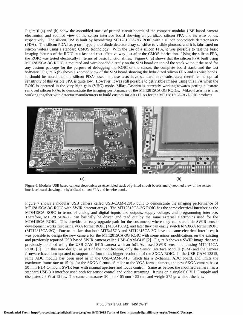
Figure 6 (a) and (b) show the assembled stack of printed circuit boards of the compact modular USB based camera
electronics, and zoomed view of the sensor interface board showing a hybridized silicon FPA and its wire bonds,
respectively. The silicon FPA is built by hybridizing MT12815CA-3G ROIC with a silicon photodiode detector array
(PDA). The silicon PDA has p-on-n type photo diode detector array sensitive to visible photons, and it is fabricated on
silicon wafers using a standard CMOS technology. With the use of a silicon FPA, it was possible to test the basic
imaging features of the ROIC in a fast and cost effective way just after the CMOS fabrication. Using the silicon FPA,
the ROIC was tested electrically in terms of basic functionalities. Figure 6 (a) shows that the silicon FPA built using
MT12815CA-3G ROIC is mounted and wire-bonded directly on the SIM board on top of the stack without the need for
any custom package for the purpose of debugging the ROIC or the sensor, the complete board stack, and the test
software. Figure 6 (b) shows a zoomed view of the SIM board showing the hybridized silicon FPA and its wire bonds.
It should be noted that the silicon PDAs used in these tests have standard thick substrates; therefore the optical
sensitivity of this visible FPA is quite low. However, it was still possible to get visible images using this FPA when the
ROIC is operated in the very high gain (VHG) mode. Mikro-Tasarim is currently working towards getting substrate
removed silicon FPAs to demonstrate the imaging performance of the MT12815CA-3G ROICs. Mikro-Tasarim is also
working together with detector manufacturers to build custom InGaAs FPAs for the MT12815CA-3G ROIC products.
(a) (b)
Figure 6. Modular USB based camera electronics: a) Assembled stack of printed circuit boards and b) zoomed view of the sensor
interface board showing the hybridized silicon FPA and its wire bonds.
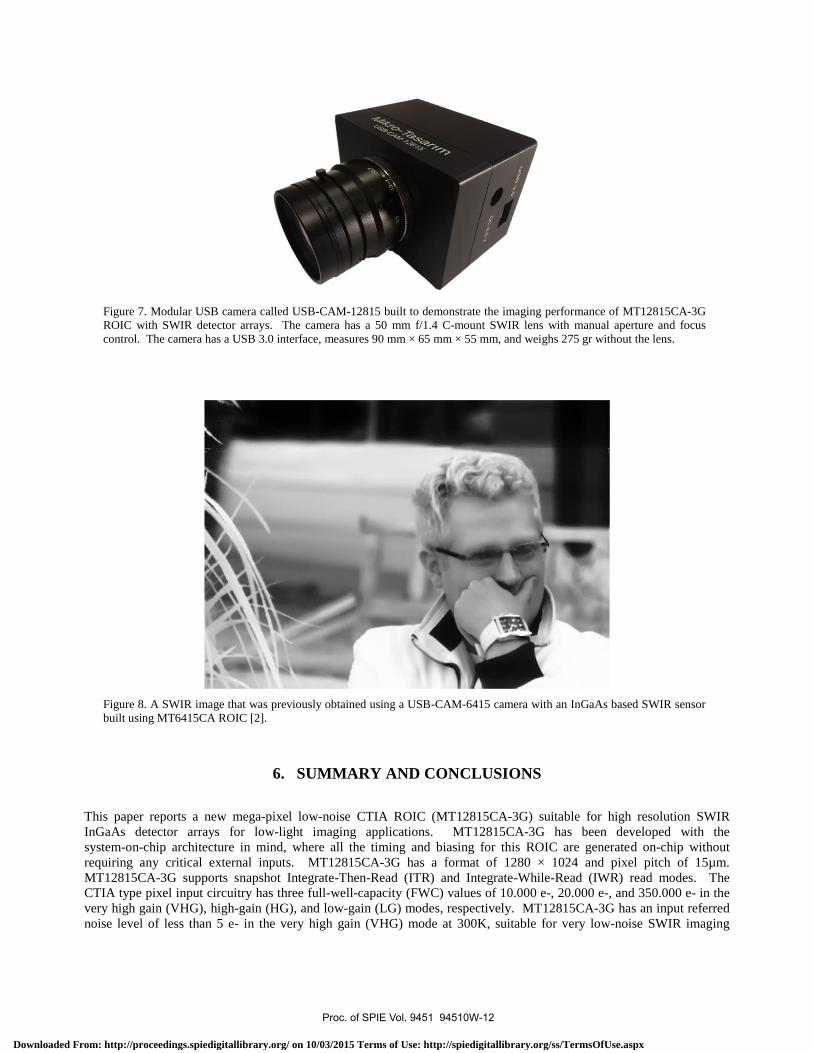
Figure 7 shows a modular USB camera called USB-CAM-12815 built to demonstrate the imaging performance of
MT12815CA-3G ROIC with SWIR detector arrays. The MT12815CA-3G ROIC has the same electrical interface as the
MT6415CA ROIC in terms of analog and digital inputs and outputs, supply voltage, and programming interface.
Therefore, MT12815CA-3G can basically be driven and read out by the same external electronics used for the
MT6415CA ROIC. This provides an easy upgrade path for the customers, where they can start their SWIR sensor
development works first using VGA format ROIC (MT6415CA), and later they can easily switch to SXGA format ROIC
(MT12815CA-3G). Due to the fact that both MT6415CA and MT12815CA-3G have the same electrical interfaces, it
was possible to design the new camera for the MT12815CA-3G ROIC with some minor modifications on the existing
and previously reported USB based SWIR camera called USB-CAM-6415 [2]. Figure 8 shows a SWIR image that was
previously obtained using the USB-CAM-6415 camera with an InGaAs based SWIR sensor built using MT6415CA
ROIC [5]. In this new design, as part of the modification, only the Sensor Interface Module (SIM) and the camera
firmware have been updated to support the four times bigger resolution of the SXGA ROIC. In the USB-CAM-12815,
same ADC module has been used as in the USB-CAM-6415, which has a 2-channel ADC board, and limits the
maximum frame rate to 15 fps for the SXGA format. Similar to the VGA format camera, the new SXGA camera has a
50 mm f/1.4 C-mount SWIR lens with manual aperture and focus control. Same as before, the modified camera has a
standard USB 3.0 interface used both for sensor control and video streaming. It runs on a single 6.0 V DC supply and
dissipates 2.3 W at 15 fps. The camera measures 90 mm × 65 mm × 55 mm and weighs 275 gr without the lens.
Proc. of SPIE Vol. 9451 94510W-11
Downloaded From: http://proceedings.spiedigitallibrary.org/ on 10/03/2015 Terms of Use: http://spiedigitallibrary.org/ss/TermsOfUse.aspx
*4 all'% IQMIMS
Figure 7. Modular USB camera called USB-CAM-12815 built to demonstrate the imaging performance of MT12815CA-3G
ROIC with SWIR detector arrays. The camera has a 50 mm f/1.4 C-mount SWIR lens with manual aperture and focus
control. The camera has a USB 3.0 interface, measures 90 mm × 65 mm × 55 mm, and weighs 275 gr without the lens.
Figure 8. A SWIR image that was previously obtained using a USB-CAM-6415 camera with an InGaAs based SWIR sensor
built using MT6415CA ROIC [2].
6. SUMMARY AND CONCLUSIONS
This paper reports a new mega-pixel low-noise CTIA ROIC (MT12815CA-3G) suitable for high resolution SWIR
InGaAs detector arrays for low-light imaging applications. MT12815CA-3G has been developed with the
system-on-chip architecture in mind, where all the timing and biasing for this ROIC are generated on-chip without
requiring any critical external inputs. MT12815CA-3G has a format of 1280 × 1024 and pixel pitch of 15µm.
MT12815CA-3G supports snapshot Integrate-Then-Read (ITR) and Integrate-While-Read (IWR) read modes. The
CTIA type pixel input circuitry has three full-well-capacity (FWC) values of 10.000 e-, 20.000 e-, and 350.000 e- in the
very high gain (VHG), high-gain (HG), and low-gain (LG) modes, respectively. MT12815CA-3G has an input referred
noise level of less than 5 e- in the very high gain (VHG) mode at 300K, suitable for very low-noise SWIR imaging
Proc. of SPIE Vol. 9451 94510W-12
Downloaded From: http://proceedings.spiedigitallibrary.org/ on 10/03/2015 Terms of Use: http://spiedigitallibrary.org/ss/TermsOfUse.aspx

applications. MT12815CA-3G has 8 analog video outputs that can be programmed in 8, 4, or 2-output modes with a
selectable analog reference for pseudo-differential operation. MT12815CA-3G is a highly configurable ROIC, whose
key features such as bias, gain, integration time, window size and location can be programmed on-the-fly through a
3-wire serial interface simplifying the overall system integration in the software controlled imaging applications. The
integration time of the ROIC can be programmed up to 1s in steps of 0.1 µs. The ROIC supports frame rate values up to
55 fps in the 8-output mode, when operated at a nominal clock frequency of 10 MHz. The ROIC uses 3.3 V and 1.8V
supply voltages and dissipates less than 350 mW in the 4-output mode. MT12815CA-3G is fabricated using a modern
mixed-signal CMOS process on 200 mm CMOS wafers, and there are 44 ROIC parts per wafer. The probe tests show
that the die yield is higher than 70%, which corresponds to more than 30 working ROIC parts per wafer typically.
MT12815CA-3G ROIC is available as tested wafers or dies, where a detailed test report and wafer map are provided for
each wafer. A compact USB 3.0 based test camera and imaging software are also available for the customers to test and
evaluate the imaging performance of SWIR sensors built using MT12815CA-3G ROICs. The camera has a 50mm f/1.4
C-mount SWIR lens with manual aperture and focus control. The camera runs on a single 6.0 V DC supply, measures
90 mm × 65 mm × 55 mm, and weighs 275 gr without the lens. Mikro-Tasarim has also recently developed a
programmable mixed-signal application specific integrated circuit (ASIC), called MTAS1410X8, which is designed to
perform ROIC driving and digitization functions for ROICs with analog outputs, such as MT12815CA-3G and
MT6415CA ROIC products of Mikro-Tasarim. MTAS1410X8 has 8 simultaneously working 14-bit analog-to-digital
converters (ADCs) with integrated programmable gain amplifiers (PGAs), video input buffers, programmable controller,
and high-speed digital video interface supporting various formats including Camera Link. MTAS1410X8 is packaged in
a plastic ball grid array (PBGA) which has a ball grid array of 16 × 16 with a pitch of 1 mm, and measures
17 mm × 17 mm. MT12815CA-3G ROIC together with MTAS1410X8 ASIC can be used to develop low-noise and
high-resolution SWIR imaging sensors with low power dissipation and reduced board area for the camera electronics.
REFERENCES
[1] Eminoglu, S., Mahsereci, Y. U., Altiner, C., and Akin, T., “MT6425CA: A 640x512-25µm CTIA ROIC for SWIR
InGaAs Detector Arrays,” Proc. SPIE 8353, 83530D (2012).
[2] Eminoglu, S., Isikhan M., Bayhan N., Gulden M. A,, Incedere O. S., Soyer S. T., et al. “MT6415CA:
A 640x512-15µm CTIA ROIC for SWIR InGaAs Detector Arrays,” Proc. SPIE 8704, 87042Z (2013).
[3] Eminoglu, S. and Akin T., “MT3250BA: A 320×256-50μm Snapshot Microbolometer ROIC for High-Resistance
Detector Arrays,” Proc. SPIE 8704, 87042Y (2013).
[4] Eminoglu, S., Gulden, M. A., Bayhan, N., Incedere, O. S., Soyer, S. T., Ustundag, C. M. B., Isikhan, M., Kocak, S.,
Turan, O., Yalcin, C., and Akin, "MT3825BA: A 384×288-25µm ROIC for Uncooled Microbolometer FPAs," Proc.
SPIE 9070, 907024 (2014).
[5] Eminoglu, S., Yimaz S. G., and Kocak S., “A Miniature VGA SWIR Camera using MT6415CA ROIC,” Proc. SPIE
9070, 90700A (2014).
[6] Ceyhan, T., “ROIC Products,” Mikro-Tasarim Ltd., 16 March 2015, <http://www.mikro-tasarim.com.tr/products>
(17 April 2015).
[7] Onat, B. M., Huang, W., Masaun, N., Lange, M., Ettenberg, M. H., and Dries, C., “Ultra Low Dark Current InGaAs
Technology for Focal Plane Arrays for Low-Light Level Visible-Shortwave Infrared Imaging,” Proc. SPIE 6542,
65420L (2007).
[8] Malchow, D., Battaglia, J., Brubaker, R., and Ettenberg, M., “High speed Short Wave Infrared (SWIR) imaging and
range gating cameras,” Proc. SPIE 6541, 654106 (2007).
[9] Hansen, M. P. and Malchow, D. S., “Overview of SWIR detectors, cameras, and applications,” Proc. SPIE 6939,
69390I (2008).
[10] MacDougal, M., Geske, J., Wang, C., and Follman, D., “Low-Light-Level InGaAs Focal Plane Arrays with and
without Illumination,” Proc. SPIE 7660, 76600K (2010).
[11] MacDougal, M., Hood, A., Geske, J., Wang, J., Patel, F., Follman, D., Manzo, J., and Getty, J., “InGaAs Focal Plan
Arrays for Low Light Level SWIR Imaging,” Proc. SPIE 8012, 801221 (2011).
[12] Holst, G. C., “An Engineer’s Approach to System Performance,” Proc. SPIE 6543, 65430A (2007).
[13] Klem, E. J. D., Lewis, J., Gregory, C., Temple, D., Wijewarnasuriya, P. S., et al. "Low-cost SWIR sensors:
advancing the performance of ROIC-integrated colloidal quantum dot photodiode arrays," Proc. SPIE 9070, 907039
(2014).
Proc. of SPIE Vol. 9451 94510W-13
Downloaded From: http://proceedings.spiedigitallibrary.org/ on 10/03/2015 Terms of Use: http://spiedigitallibrary.org/ss/TermsOfUse.aspx