Embed Size (px)
Citation preview
227
A 100 kJ Pulse Unit for Electromagnetic Forming of Large Area Sheet Metals P
∗P
W. Hartmann P
1P, M. RömheldP
1P, A. Donner P
2
P
1P Siemens AG, Corporate Technology, CT PS 5, Erlangen, Germany
P
2P Siemens AG, Automation and Drives, A&D MC RD 8, Chemnitz, Germany
Abstract
Magnetoforming of tube or sheet metal parts can significantly extend the range of geometries conceivable with state-of-the-art forming methods. A major advantage is the considerably higher forming speed of the process achievable by using a magnetic piston without inertia. Key for this technology is the development of reliable, long-lifetime, high current pulse power generators able to deliver tens to hundreds of kiloamps of peak current to a mainly inductive load which is highly variable in time during the forming process. A high-current, high energy pulse generator for electromagnetic forming of large area sheet metal has been developed and was taken into operation. Design criteria were reliability and safety for all possible load cases, including short circuits and short-circuiting loads under operation, at nominal peak currents of up to 200 kA and peak pulse energies of up to 100 kJ. In order to comply with the safety requirements, an all-solid-state design has been chosen using high power semiconductor switches for pulse forming instead of ignitrons or spark gaps. Due to constraints concerning space and manageability, the coupling between the load and the pulse forming unit is achieved via a semi-rigid bundle of high voltage cables, allowing an adjustment of the carrier of the forming coil while being electrically connected to each other. We report on the development of a pulse generator for peak currents of 50 kA to up to 200 kA at a pulse width of typically around 100 µs, depending on the load parameters. In order to meet lifetime requirements suitable for industrial applications, the short circuit handling capability of peak currents of up to 450 kA is a major issue in the pulse generator design. A modular 3-branch design of parallel capacitor banks has been adopted to achieve the requirements concerning reliability, lifetime, and short circuit handling. The prototype pulse generator is based upon off-the-shelf devices, including high-current semiconductor switches. First operating results of the commissioning phase of the installation are reported.
1 This work was supported by the “Sächsische Aufbaubank” within the framework of a joined project between IWU (Chemnitz), Siemens AG (Erlangen, Chemnitz), H&T (Zwickau), and Volkswagen AG (Wolfsburg)
brought to you by COREView metadata, citation and similar papers at core.ac.uk
provided by Eldorado - Ressourcen aus und für Lehre, Studium und Forschung
2nd International Conference on High Speed Forming – 2006
228
Keywords:
Pulse generator, Magnetoforming, Solid-state switch
1 Introduction
Magnetoforming is a well-known metal forming process which has been in industrial use for decades. Up to now, however, the major range of applications is limited to coaxial forming of tube-like parts, whereas sheet metal forming has been developed to larger cross-sectional areas only recently [1]. The main reason for this limitation is that sheet metal forming requires considerably higher pulse energies than coaxial forming due to the large cross-sectional areas usually involved in flat workpieces. For an appropriate acceleration of sheet metal parts to velocities on the order of > 200 m/s sufficient for impact forming in a suitable matrix [2] peak pressures on the order of >200 bars are needed at risetimes of a few tens of microseconds only. Peak currents on the order of > 50 kA up to 200 kA are therefore necessary in order to process large area workpieces. In this work, we report on the feasibility of a fully solid-state pulse generator with corresponding high peak currents of up to 200 kA nominal current at a pulse width on the order of 100 µs FWHM (full width at half maximum). Due to the low inductance of the pulse generator the peak current in the system can reach more than 400 kA during a short circuit in the load or at the transmission line between pulse generator and the driving magnetic field coil. Such a system failure must be regarded as a regularly occurring phenomenon at least during the development and test phase of the generator and drive coil and, thus, must be safely handled by all system components. Care has therefore been taken to design a system which inherently tolerates such a failure by limiting the peak electrical stress to the safe operating areas of the specific components. During normal operation the load inductance varies rapidly due to the moving workpiece which is accelerated by the magnetic force. The generator is therefore subjected to rapidly changing load impedance, from close to short circuit to an impedance which is large as compared with the generator internal impedance. The circuit design is chosen such as to tolerate this variation under all operating circumstances. A modular design with three parallel sub-modules has been adopted to achieve the requirements concerning reliability, lifetime, and short circuit handling. The prototype design is based upon off-the-shelf devices, including high-current discharge switches based on semiconductor devices. The basic concept of the pulse generator is presented, including results from extensive circuit modeling concerning nominal performance as well as short circuit behavior.
2 Circuit design
The pulse generator is intended to be used under a broad variation of load parameters; to support this requirement, the nominal data of the pulse generator were chosen as follows: Peak current 50 to > 200 kA typ. Pulse duration 80 µs typ. FWHM
2nd International Conference on High Speed Forming – 2006
229
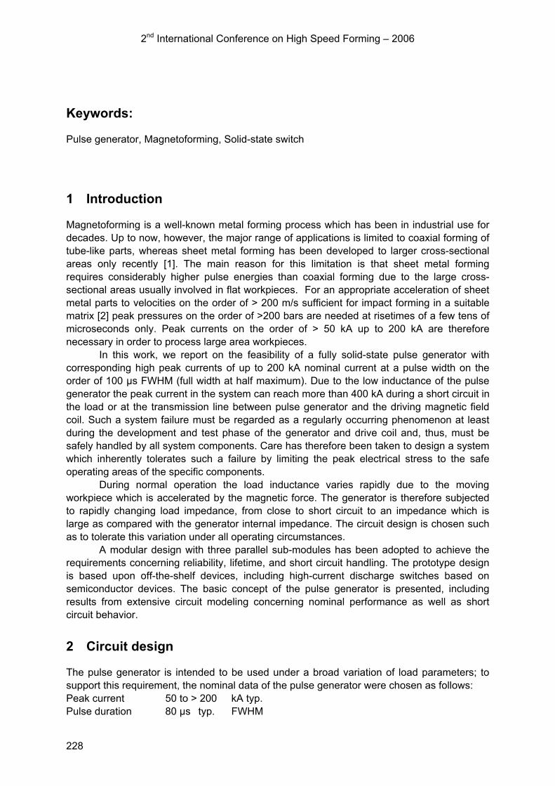
Load inductance 1 to >10 µH Lifetime > 10.000 pulses Short circuit current < 450 kA peak The restrictions on switches, lifetime, and components are caused by the requirements of minimal maintenance and costs, maximum safety, and reliability under industrial constraints, while the electrical data are derived from a preliminary estimate of the necessary peak currents and current rates of rise. A. Pulse generator design A modular design of a capacitor bank with three parallel sub-modules has been described in [3] to achieve the requirements and is shown schematically in figure 1a. Each module accommodates its own combination of switch and crowbar diode S1/D1... S3/D3 in order to limit the peak stress of these components to be within their SOA (safe operating area). Each sub-module contains a multitude of parallel capacitors; modularity can be achieved by adding or removing individual capacitor banks, which opens up the possibility to vary the impedance of the pulse generator.
Figure 1: Equivalent circuit of the pulse generator circuit design 1a, (left) based on a capacitor bank with three parallel sub-modules, each equipped with its own switch S1 to S3 and crowbar diode D1 to D3 respectively. LCx: ≈1.5 µH, series inductance of the individual capacitor banks. 1b, right: View into the pulse generator showing two of three rows of capacitors with busbars, current leads, and current limiting / balancing resistors
The low side of the three sub-modules C1...C3 is directly connected to the load inductance L Bload B by a busbar in a hard-wired fashion. Therefore, the output is nominally grounded by the series load inductance (drive coil) and is only exposed to high voltage during the current pulse. The high sides of the sub-modules are charged in parallel through a single high voltage power supply V1 and are de-coupled from each other during the pulse by series charging resistors R BchB. The pulse generator output is connected to the coil via a low impedance cable transmission line, which is also exposed to high voltage stress only briefly during the pulse. An end-on view into the pulse generator is shown in fig. 1b. Semiconductor switches made from stacks of high power, and high voltage thyristors are used in this circuit design, with peak currents in the short circuit case of less than 150 kA per switch [4]. Such elements are commercially available by several companies, including ABB, DYNEX, EUPEC, NKG, and Westcode, in the form of individual components or even as
C 1 2 -2 1 kV L C 1
T r igg er
R c h3
S 3 /D 3
L C 3
load
S 1 /D 1
S 2 /D 2
C 2
C 3
R c h2
R c h1
L C 2
2nd International Conference on High Speed Forming – 2006
230
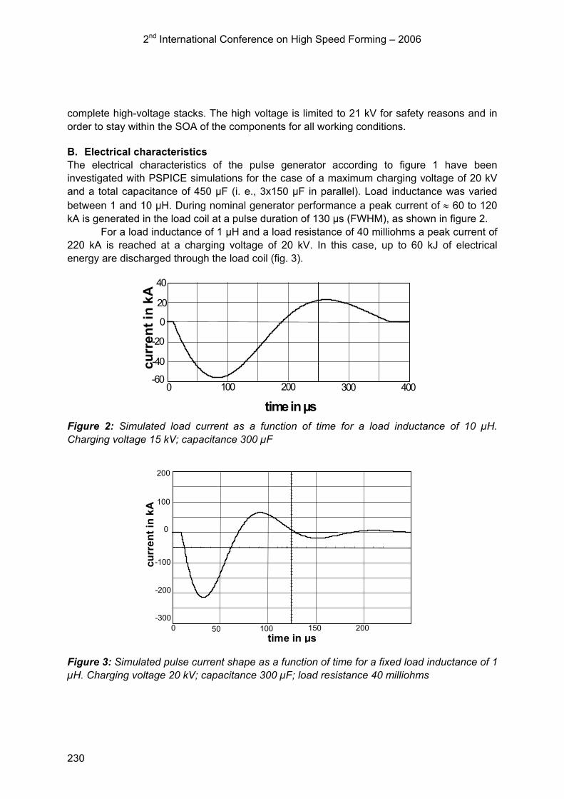
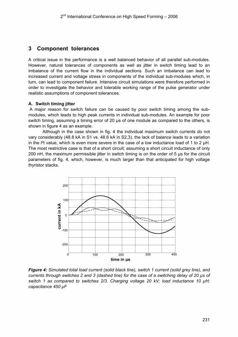
complete high-voltage stacks. The high voltage is limited to 21 kV for safety reasons and in order to stay within the SOA of the components for all working conditions. B. Electrical characteristics The electrical characteristics of the pulse generator according to figure 1 have been investigated with PSPICE simulations for the case of a maximum charging voltage of 20 kV and a total capacitance of 450 µF (i. e., 3x150 µF in parallel). Load inductance was varied between 1 and 10 µH. During nominal generator performance a peak current of ≈ 60 to 120 kA is generated in the load coil at a pulse duration of 130 µs (FWHM), as shown in figure 2. For a load inductance of 1 µH and a load resistance of 40 milliohms a peak current of 220 kA is reached at a charging voltage of 20 kV. In this case, up to 60 kJ of electrical energy are discharged through the load coil (fig. 3).
Figure 2: Simulated load current as a function of time for a load inductance of 10 µH. Charging voltage 15 kV; capacitance 300 µF
Figure 3: Simulated pulse current shape as a function of time for a fixed load inductance of 1 µH. Charging voltage 20 kV; capacitance 300 µF; load resistance 40 milliohms
curr
enti
nkA
-20
-40
-60
0
20
40
time in µs4003002001000
0time in µs
100
200
curr
ent i
n kA
0
-200
-100
50 200100 150-300
2nd International Conference on High Speed Forming – 2006
231
3 Component tolerances
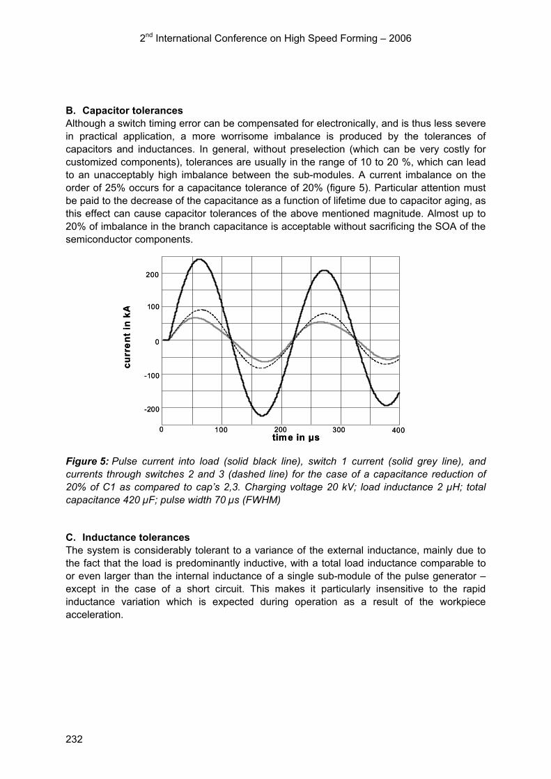
A critical issue in the performance is a well balanced behavior of all parallel sub-modules. However, natural tolerances of components as well as jitter in switch timing lead to an imbalance of the current flow in the individual sections. Such an imbalance can lead to increased current and voltage stress in components of the individual sub-modules which, in turn, can lead to component failure. Intensive circuit simulations were therefore performed in order to investigate the behavior and tolerable working range of the pulse generator under realistic assumptions of component tolerances. A. Switch timing jitter A major reason for switch failure can be caused by poor switch timing among the sub-modules, which leads to high peak currents in individual sub-modules. An example for poor switch timing, assuming a timing error of 20 µs of one module as compared to the others, is shown in figure 4 as an example. Although in the case shown in fig. 4 the individual maximum switch currents do not vary considerably (48.8 kA in S1 vs. 48.6 kA in S2,3), the lack of balance leads to a variation in the I²t value, which is even more severe in the case of a low inductance load of 1 to 2 µH. The most restrictive case is that of a short circuit; assuming a short circuit inductance of only 200 nH, the maximum permissible jitter in switch timing is on the order of 5 µs for the circuit parameters of fig. 4, which, however, is much larger than that anticipated for high voltage thyristor stacks.
Figure 4: Simulated total load current (solid black line), switch 1 current (solid grey line), and currents through switches 2 and 3 (dashed line) for the case of a switching delay of 20 µs of switch 1 as compared to switches 2/3. Charging voltage 20 kV; load inductance 10 µH; capacitance 450 µF
time in µs
200
curr
ent i
n kA
100
0
-100
-200
0 100 200 300 400
2nd International Conference on High Speed Forming – 2006
232
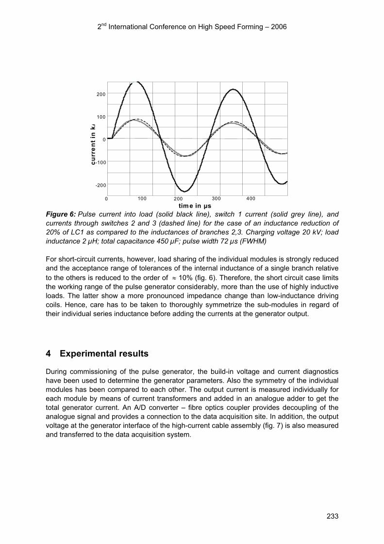
B. Capacitor tolerances Although a switch timing error can be compensated for electronically, and is thus less severe in practical application, a more worrisome imbalance is produced by the tolerances of capacitors and inductances. In general, without preselection (which can be very costly for customized components), tolerances are usually in the range of 10 to 20 %, which can lead to an unacceptably high imbalance between the sub-modules. A current imbalance on the order of 25% occurs for a capacitance tolerance of 20% (figure 5). Particular attention must be paid to the decrease of the capacitance as a function of lifetime due to capacitor aging, as this effect can cause capacitor tolerances of the above mentioned magnitude. Almost up to 20% of imbalance in the branch capacitance is acceptable without sacrificing the SOA of the semiconductor components.
Figure 5: Pulse current into load (solid black line), switch 1 current (solid grey line), and currents through switches 2 and 3 (dashed line) for the case of a capacitance reduction of 20% of C1 as compared to cap’s 2,3. Charging voltage 20 kV; load inductance 2 µH; total capacitance 420 µF; pulse width 70 µs (FWHM) C. Inductance tolerances The system is considerably tolerant to a variance of the external inductance, mainly due to the fact that the load is predominantly inductive, with a total load inductance comparable to or even larger than the internal inductance of a single sub-module of the pulse generator – except in the case of a short circuit. This makes it particularly insensitive to the rapid inductance variation which is expected during operation as a result of the workpiece acceleration.
time in µs
-200
-100
200
curr
ent i
n kA
0
100
0 100 200 300 400time in µs
-200
-100
200
curr
ent i
n kA
0
100
0 100 200 300 400
2nd International Conference on High Speed Forming – 2006
233
Figure 6: Pulse current into load (solid black line), switch 1 current (solid grey line), and currents through switches 2 and 3 (dashed line) for the case of an inductance reduction of 20% of LC1 as compared to the inductances of branches 2,3. Charging voltage 20 kV; load inductance 2 µH; total capacitance 450 µF; pulse width 72 µs (FWHM) For short-circuit currents, however, load sharing of the individual modules is strongly reduced and the acceptance range of tolerances of the internal inductance of a single branch relative to the others is reduced to the order of ≈ 10% (fig. 6). Therefore, the short circuit case limits the working range of the pulse generator considerably, more than the use of highly inductive loads. The latter show a more pronounced impedance change than low-inductance driving coils. Hence, care has to be taken to thoroughly symmetrize the sub-modules in regard of their individual series inductance before adding the currents at the generator output.
4 Experimental results
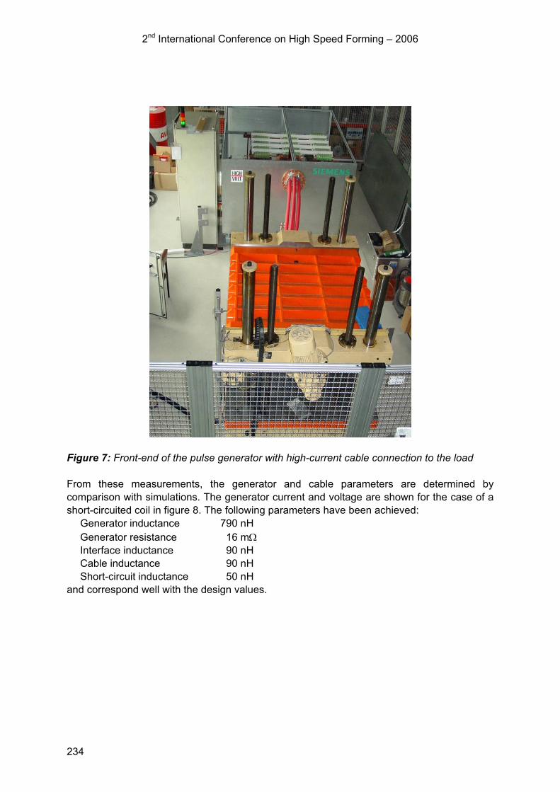
During commissioning of the pulse generator, the build-in voltage and current diagnostics have been used to determine the generator parameters. Also the symmetry of the individual modules has been compared to each other. The output current is measured individually for each module by means of current transformers and added in an analogue adder to get the total generator current. An A/D converter – fibre optics coupler provides decoupling of the analogue signal and provides a connection to the data acquisition site. In addition, the output voltage at the generator interface of the high-current cable assembly (fig. 7) is also measured and transferred to the data acquisition system.
time in µs
-200
-100
0
100
200cu
rren
t in
kA
0 100 200 300 400
2nd International Conference on High Speed Forming – 2006
234
Figure 7: Front-end of the pulse generator with high-current cable connection to the load
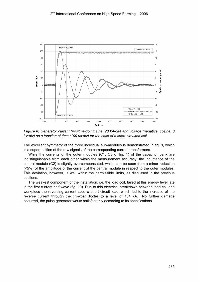
From these measurements, the generator and cable parameters are determined by comparison with simulations. The generator current and voltage are shown for the case of a short-circuited coil in figure 8. The following parameters have been achieved:
Generator inductance 790 nH Generator resistance 16 mΩ Interface inductance 90 nH Cable inductance 90 nH Short-circuit inductance 50 nH
and correspond well with the design values.
2nd International Conference on High Speed Forming – 2006
235
-100
-80
-60
-40
-20
0
20
40
60
80
100
120
-200 0 200 400 600 800 1000 1200 1400 1600 1800
Zeit / µs
Str
om /
kA
-15
-12
-9
-6
-3
0
3
6
9
12
15
18
Spul
ensp
annu
ng /
kV
<I(ges)> - I(0)<I(Maxhold)> -I(Maxhold,0)<U(Spule)> - U(0)
I(Max) = 102.9 kA
U(Min) = -13.3 kV
I(Maxhold) = 95.3
Figure 8: Generator current (positive-going sine, 20 kA/div) and voltage (negative, cosine, 3 kV/div) as a function of time (100 µs/div) for the case of a short-circuited coil
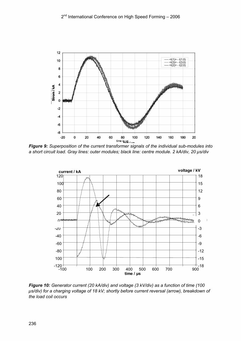
The excellent symmetry of the three individual sub-modules is demonstrated in fig. 9, which is a superposition of the raw signals of the corresponding current transformers.
While the currents of the outer modules (C1, C3 of fig. 1) of the capacitor bank are indistinguishable from each other within the measurement accuracy, the inductance of the central module (C2) is slightly overcompensated, which can be seen from a minor reduction (<5%) of the amplitude of the current of the central module in respect to the outer modules. This deviation, however, is well within the permissible limits, as discussed in the previous sections.
The weakest component of the installation, i.e. the load coil, failed at this energy level late in the first current half wave (fig. 10). Due to this electrical breakdown between load coil and workpiece the reversing current sees a short circuit load, which led to the increase of the reverse current through the crowbar diodes to a level of 104 kA. No further damage occurred, the pulse generator works satisfactorily according to its specifications.
2nd International Conference on High Speed Forming – 2006
236
-8
-6
-4
-2
0
2
4
6
8
10
12
-20 0 20 40 60 80 100 120 140 160 180 20
Zeit / µs
Stro
m /
kA
<I(1)> - I(1;0)<I(3)> - I(3;0)<I(2)> - I(2;0)
curr
ent i
n kA
time in µs
-8
-6
-4
-2
0
2
4
6
8
10
12
-20 0 20 40 60 80 100 120 140 160 180 20
Zeit / µs
Stro
m /
kA
<I(1)> - I(1;0)<I(3)> - I(3;0)<I(2)> - I(2;0)
curr
ent i
n kA
time in µs Figure 9: Superposition of the current transformer signals of the individual sub-modules into a short circuit load. Gray lines: outer modules; black line: centre module. 2 kA/div, 20 µs/div
Figure 10: Generator current (20 kA/div) and voltage (3 kV/div) as a function of time (100 µs/div) for a charging voltage of 18 kV; shortly before current reversal (arrow), breakdown of the load coil occurs
-120
100
-80
-60
-40
-20
20
40
60
80
100
120
-100 100 200 300 400 500 600 700 900 time / µs
-18
-15
-12
-9
-6
-3
3
6
9
12
15
18 voltage / kVcurrent / kA
00
2nd International Conference on High Speed Forming – 2006
237
5 Summary
A high current pulse generator for magnetoforming of sheet metal parts has successfully been developed and commissioned. The design is based on the use of commercial, off-the-shelf components and a modular architecture of the capacitor bank. The most critical design parameters are • the ability to withstand short-circuit loads and the corresponding high peak currents, • tolerances of switch timing jitter, and • tolerances of the internal inductance of the parallel branches of the capacitor bank.
With careful design of the coupling section between the three sub-modules a sufficiently high symmetry between the sub-modules better than ± 5% has been achieved for the case of a short circuit load. The pulse generator operates satisfactorily to its specifications, including the flexible high-current cable connection between pulse generator and load. High-power semiconductor switches are a key component of this generator.
References
[1] Daehn, G. S. et al.: Improved Formability with Electromagnetic Forming: Fundamentals and a Practical Example. http://www.er6.eng.ohio-state.edu/%7Edaehn/overview/ index.htm, (2003)
[2] Badelt, M.; Beerwald, C.; Brosius, A.; Kleiner, M.: Process analysis of electromagnetic sheet metal forming by online-measurement and finite element simulation. 6P
thP
ESAFORM Conference on Material Forming, Salerno, Italy, April 28-30 (2003) [3] Hartman, W.; Roemheld, M.: Design of a high current pulse generator for
Magnetoforming. Proceedings 26P
thP IEEE Power Modulator Symposium, San Francisco,
CA, USA (2004), pp. 310-313 [4] Welleman, A. et al.: Semiconductor switches for single pulse and repetitive pulse
applications. 4th Int. AECV Conference, The Netherlands, Sept. 24 – 26 (2001)