Embed Size (px)
Citation preview
A 10 to 11.5GHz Rotational Phase and Frequency Detector for Clock Recovery Circuit
Fan-Ta Chen, Min-Sheng Kao, Yu-Hao Hsu, Chih-Hsing Lin,
Jen-Ming Wu, Ching-Te Chiu, Shuo-Hung Hsu Institute of Communications Engineering, National Tsing Hua University, Hsinchu, 300, Taiwan.
E-mail:[email protected]
Abstract—This paper presents a 10.0~11.5 Gb/s full-rate phase and frequency detector integrated with the clock recovery circuit (CRC) for application in optical receivers. A rotational phase and frequency detector (RPFD) without external reference clock is proposed to train the conventional bang-bang phase detector (BBPD) to capture the clock frequency. The proposed RPFD shows 1.5 GHz capture range and works in the high speed data rate of 10 Gb/s. Only one closed loop is used to track the internal clock. The acquisition time for the clock frequency to adjust from 11.5 to 10 GHz is 160 ns. The fabricated chip occupies 0.7 mm2 in 90 nm CMOS process with −108.8 dBc/Hz at 1-MHz offset and consumes 52 mW power with 1.0-V supply.
I. INTRODUCTION The fast tracking for high speed clock recovery saves
numbers of reserving bits time in the global internet receiver. The conventional clock recovery circuit (CRC) adopts phase locked loops (PLL) and frequency locked loops (FLL) as phase and frequency correction.
An ideal bang-bang phase detector (BBPD) [1] characteristic produces a sign function that it rapidly increases output from negative to positive value while the phase difference (Δφ) comes to zero. The PLL synchronizes the input data with the internal clock when the recovered clock triggers in this area. However, the initial clock frequency differs from the input data rate. Although the BBPD is capable of capturing the frequency near the data rate, the truth is that the untrained clock has possible to lock at a metastable frequency. Furthermore, the tracking time is limited to the loop bandwidth and trades off with the jitter performance. For these reasons, recent literatures have engaged in adding a frequency detector (FD) for locking sequentially PLL and FLL [2] or choosing lower bandwidth for FLL [3]. However, dual loops design increases the inconvenience and complexity for the next generation of wire-line communication system.
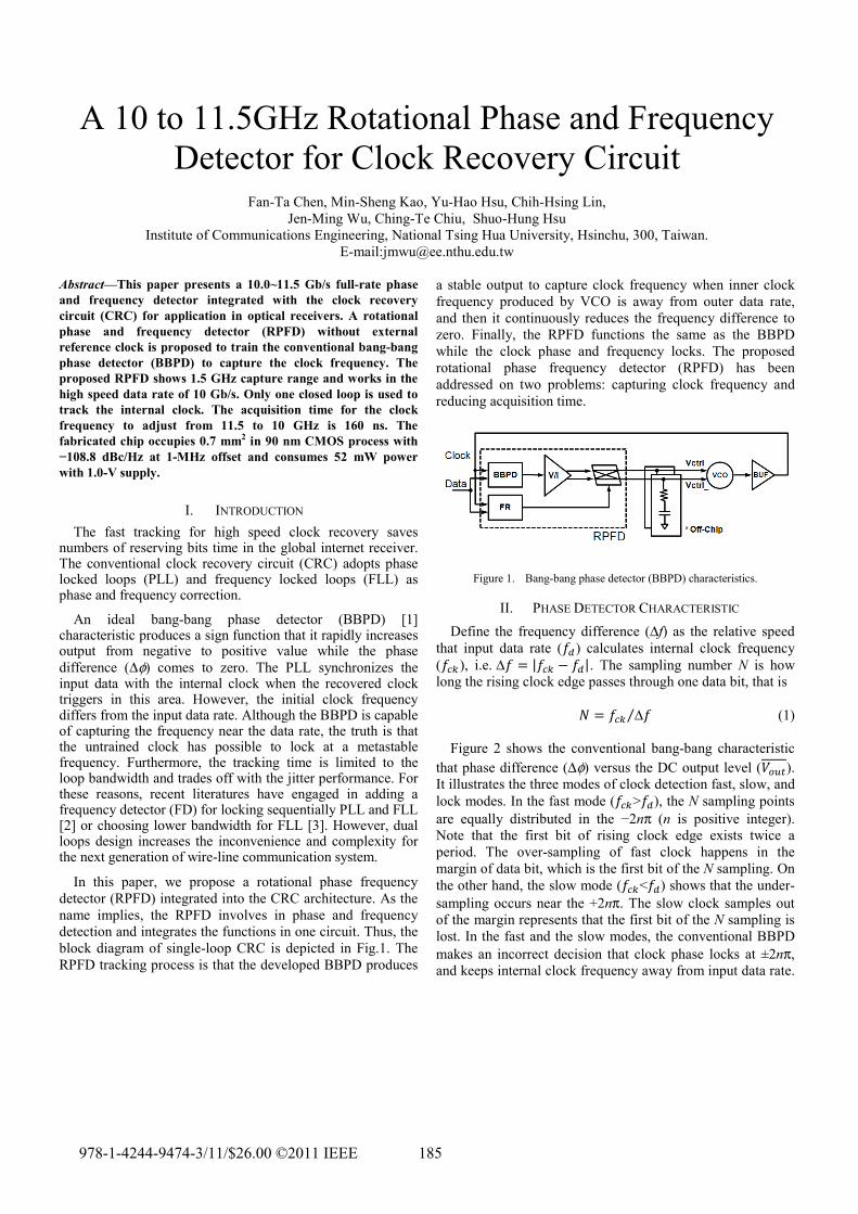
In this paper, we propose a rotational phase frequency detector (RPFD) integrated into the CRC architecture. As the name implies, the RPFD involves in phase and frequency detection and integrates the functions in one circuit. Thus, the block diagram of single-loop CRC is depicted in Fig.1. The RPFD tracking process is that the developed BBPD produces
a stable output to capture clock frequency when inner clock frequency produced by VCO is away from outer data rate, and then it continuously reduces the frequency difference to zero. Finally, the RPFD functions the same as the BBPD while the clock phase and frequency locks. The proposed rotational phase frequency detector (RPFD) has been addressed on two problems: capturing clock frequency and reducing acquisition time.
Figure 1. Bang-bang phase detector (BBPD) characteristics.
II. PHASE DETECTOR CHARACTERISTIC Define the frequency difference (Δf) as the relative speed
that input data rate ( ) calculates internal clock frequency ( ), i.e. Δ | |. The sampling number N is how long the rising clock edge passes through one data bit, that is
Δ⁄ (1)
Figure 2 shows the conventional bang-bang characteristic that phase difference (Δφ) versus the DC output level ( ). It illustrates the three modes of clock detection fast, slow, and lock modes. In the fast mode ( > ), the N sampling points are equally distributed in the −2nπ (n is positive integer). Note that the first bit of rising clock edge exists twice a period. The over-sampling of fast clock happens in the margin of data bit, which is the first bit of the N sampling. On the other hand, the slow mode ( < ) shows that the under-sampling occurs near the +2nπ. The slow clock samples out of the margin represents that the first bit of the N sampling is lost. In the fast and the slow modes, the conventional BBPD makes an incorrect decision that clock phase locks at ±2nπ, and keeps internal clock frequency away from input data rate.
978-1-4244-9474-3/11/$26.00 ©2011 IEEE 185
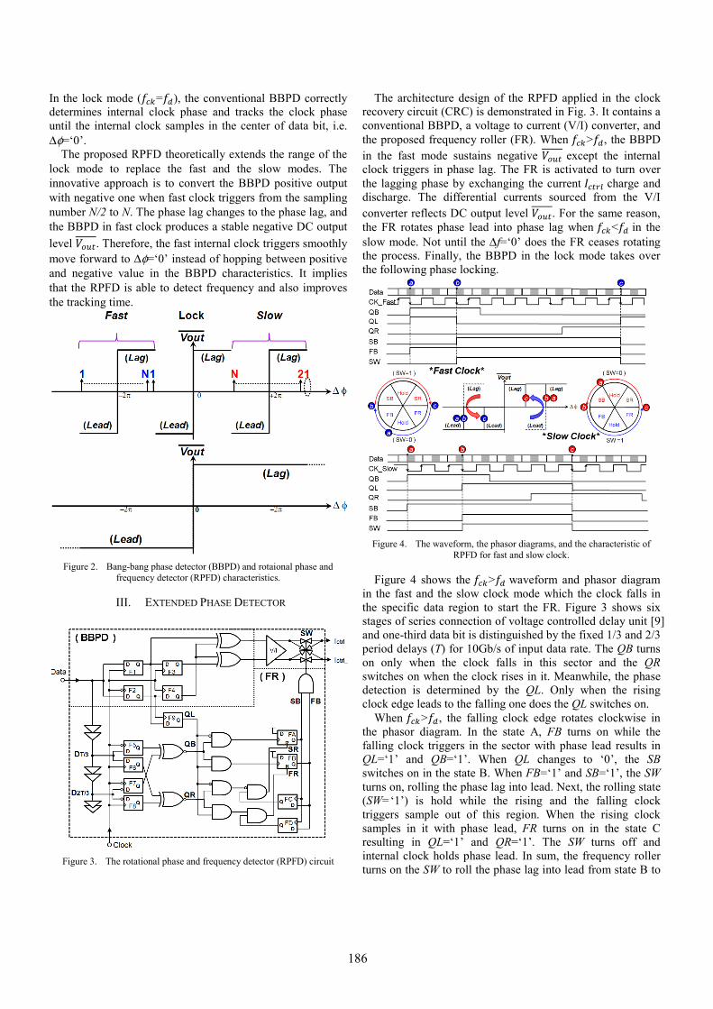
In the lock mode ( = ), the conventional BBPD correctly determines internal clock phase and tracks the clock phase until the internal clock samples in the center of data bit, i.e. Δφ=‘0’.
The proposed RPFD theoretically extends the range of the lock mode to replace the fast and the slow modes. The innovative approach is to convert the BBPD positive output with negative one when fast clock triggers from the sampling number N/2 to N. The phase lag changes to the phase lag, and the BBPD in fast clock produces a stable negative DC output level . Therefore, the fast internal clock triggers smoothly move forward to Δφ=‘0’ instead of hopping between positive and negative value in the BBPD characteristics. It implies that the RPFD is able to detect frequency and also improves the tracking time.
Figure 2. Bang-bang phase detector (BBPD) and rotaional phase and
frequency detector (RPFD) characteristics.
III. EXTENDED PHASE DETECTOR
Figure 3. The rotational phase and frequency detector (RPFD) circuit
The architecture design of the RPFD applied in the clock recovery circuit (CRC) is demonstrated in Fig. 3. It contains a conventional BBPD, a voltage to current (V/I) converter, and the proposed frequency roller (FR). When > , the BBPD in the fast mode sustains negative except the internal clock triggers in phase lag. The FR is activated to turn over the lagging phase by exchanging the current charge and discharge. The differential currents sourced from the V/I converter reflects DC output level . For the same reason, the FR rotates phase lead into phase lag when < in the slow mode. Not until the Δf=‘0’ does the FR ceases rotating the process. Finally, the BBPD in the lock mode takes over the following phase locking.
Figure 4. The waveform, the phasor diagrams, and the characteristic of
RPFD for fast and slow clock.
Figure 4 shows the > waveform and phasor diagram in the fast and the slow clock mode which the clock falls in the specific data region to start the FR. Figure 3 shows six stages of series connection of voltage controlled delay unit [9] and one-third data bit is distinguished by the fixed 1/3 and 2/3 period delays (T) for 10Gb/s of input data rate. The QB turns on only when the clock falls in this sector and the QR switches on when the clock rises in it. Meanwhile, the phase detection is determined by the QL. Only when the rising clock edge leads to the falling one does the QL switches on.
When > , the falling clock edge rotates clockwise in the phasor diagram. In the state A, FB turns on while the falling clock triggers in the sector with phase lead results in QL=‘1’ and QB=‘1’. When QL changes to ‘0’, the SB switches on in the state B. When FB=‘1’ and SB=‘1’, the SW turns on, rolling the phase lag into lead. Next, the rolling state (SW=‘1’) is hold while the rising and the falling clock triggers sample out of this region. When the rising clock samples in it with phase lead, FR turns on in the state C resulting in QL=‘1’ and QR=‘1’. The SW turns off and internal clock holds phase lead. In sum, the frequency roller turns on the SW to roll the phase lag into lead from state B to
186

state C and the RPFD outputs completely phase lead when internal fast clock comes in.
On the other hand, when , the falling clock edge counter-clockwise rotates in the phasor diagram. The falling clock samples in the sector with phase lags results in SB turns on in the state A. When QL transits to ‘1’, the SW turns on in the state B. Not until the QL turn off does the SR turn on to reset the SW. As a result, the frequency roller changes the phase lead from state B to state C and keeps the lagging phase from state C to state B. In conclusion, internal clock speed is able to be detected by RPFD that frequency roller achieves identical phase shift.
The output clock of CRC is synthesized by the LC-tank VCO to produce a pair of clock signals. Figure 5 shows the circuit schematic circuit diagram of the VCO [5] and clock buffer. The cross coupled pair of M1-M4 provides the activating gain to ensure the VCO oscillation. The differential voltage Vctrl produced by the RPFD linearly tunes the varactors to chase the phase and the frequency of the input data. Finally, the differential output Clock provides a high speed clock between 9.5 and 11.5 GHz to drive the DFF clocks in the RPFD, and the closed loop of CRC is realized.
Figure 5. The cross-couple pair LC-tank VCO with inductive load buffer.
IV. MEASUREMENT RESULT
To prove the RPFD functionality, a CRC as shown in Fig.6 is fabricated in a TSMC 1P9M 90 nm CMOS process with the overall chip size of 0.7 mm2. This chip consists of a LC-tank VCO, an inductive load buffer, and the proposed RPFD. To save chip area, the second order loop filter is chosen off-chip design. The free-running LC-tank VCO exhibits the capture range from 9.5 to 11.5 GHz with the tuning range from 0 to 1.0 V. The off-chip loop filter adopts R=200 Ω and C=6 nF, respectively. It results in loop bandwidth of 50MHz. Using the ultra low threshold CMOS provided by TSMC, the input supply voltage can be reduced to 1.0-V and results in the overall power consumption of 52 mW.
Figure 7 shows the environment that input data provided by (Anritsu MT1810A) and the output clock measured by using the signal source analyzer (Agilent E5052B) with a divided-by-two prescaler (Centellax UXD20P), and the measured clock frequency is considered twice in the real
case. Figure 8 shows the clock acquisition of the CRC while internal clock frequency is away from the input data rate with roughly 1.5 GHz. With a 231-1 PRBS, the input data rate varies from 11.46 to 9.92 Gb/s results that the CRC takes 160 ns to track the recovered clock. On the other hand, the input data changes from 10.08 to 11.48 Gb/s results in the locking time of 400ns. To consider the target data rate varying far from the previous frequency, the periodic delay (T) chosen by clock frequency of 10 GHz degenerates the final acquisition time. Therefore, the acquisition time of the CRC increases because of the glitch in the transition of frequency hopping.
Figure 6. Die microgram of the CRC with bounding wire.
Figure 7. Measurement enviroment.
Figure 8. Measured acquisition when internal clock starts from fast and
slow frequency.
187

Figure 9. Measured the internal clock of spectrum, phase noise, and
histogram.
Figure 9 shows the measured result when the recovered clock rising triggers in the centers of 10 Gb/s of input data and the FR stops rotating the phase. The recovered clock shows the frequency domain noise with −108.8 dBc/Hz of phase noise at 1 MHz offset. The time domain noise for the root mean square and the peak to peak jitters are 683 fs and 5.27 ps, respectively. The overall performance summary is listed in Table.I as follow:
TABLE I. CRC PERFORMANCE SUMMARY
CRC Characteristics
Operation Frequency 10~11.5 GHz
Recovered Data 10 Gb/s
Phase Noise at 1MHz offset −108.8 dBc / Hz
Clock Jitter for PRBS 231-1
5.26 ps (P-P)
683 fs (RMS)
Power without Buffer 52 mW@ 10 GHz
Supply voltage 1.0 v
Core area 770 μm × 920 μm
Technology 90 nm Standard CMOS
V. DISCUSSION
To avoid the frequency locked loop (FLL) to contribute
additional clock jitter in the VCO, the conventional frequency detector usually sacrifices the loop bandwidth in exchange for noise tolerance [2][3]. The disadvantage is the longer acquisition time in the smaller loop bandwidth of FLL than that of phase locked loop (PLL), i.e. tracking time of 3.89μs at 1.25Gb/s data rate [2]. This work proposes a unique way that PLL and FLL share the same loop to save chip area. Thus, the FLL has the same loop bandwidth as the PLL does. The limitation of tracking time is relaxed because PLL has the bigger loop bandwidth. On the other side, the FR makes the accurate overturn as long as the fast clock rotates clockwise, and so does the slow clock revolve counter-clockwise. As a result, the frequency capture range is between −50% and +50%, and the RPFD has the same capture range as conventional rotational frequency detector
(RFD) which operates at 2.5 Gb/s [4]. The comparison results are listed in Table II.
TABLE II. CRC COMPARISON
[2] [3] [4] This work
Technology 180 nm 180 nm 350 nm 90 nm
Acquisition
Time 3.89 μs 80 μs 800 μs 160 ns
Speed 1.25 Gb/s 3.125 Gb/s 2.5 Gb/s 10 Gb/s
Die Area 0.13 mm2 0.88 mm2 9 mm2 0.7 mm2
VI. CONCLUSION
A rotational phase and frequency detector trains the conventional bang-bang phase detector to capture the clock frequency by rolling the clock phase. Only one closed loop corresponds to track the internal clock and exhibits the acquisition time of 160ns varying the clock frequency from 11.5 to 10GHz.
ACKNOWLEDGEMENTS The authors would like to thank the National Chip Implementation Center (CIC) and Taiwan Semiconductor Manufacturing Company (TSMC) for chip fabrication.
REFERENCES [1] J. D. H. Alexander, “Clock Recovery from Random Binary Data,”
IEEE Electronics Letters, Vol. 11, pp. 541–542, Oct. 1975. [2] Woo, Jong-Kwan; Lee, Hyunjoong; Shin, Woo-Yeol; Song, Heesoo;
Jeong, Deog-Kyoon; Kim, Suhwan; “A Fast-Locking CDR Circuit with an Autonomously Reconfigurable Charge Pump and Loop Filter” IEEE Asia Solid States Circuits Conference (A-SSCC), 2006, pp 411 – 414.
[3] Rong-Jyi Yang; Kuan-Hua Chao; Sy-Chyuan Hwu; Chuan-Kang Liang; Shen-Iuan Liu “A 155.52 mbps-3.125 Gb/s continuous-rate clock and data recovery circuit” IEEE J. Solid-State Circuits, Vol. 41, no. 6, pp.1380 – 1390, June 2006.
[4] C. Kwet, E. Evans, M. Ferriss, D. Hitchcox, P. Murray, S. Selvanayagam, P. Shepherd, L. DeVito, and D. Dalton, “A 12.5-Mb/s to 2.7-Gb/s continuous-rate CDR with automatic frequency acquisition and data-rate readback,” IEEE J. Solid-State Circuits, vol. 40, no. 12, pp. 2713–2725, Dec. 2005.
[5] Ohtomo, Nishimura, Masafumi “A 12.5-Gb/s Parallel Phase Detection Clock and Data Recovery Circuit in 0.13-um CMOS” IEEE J. Solid-State Circuits, Vol. 41, no. 9, SEP 2006
[6] Jafar Savoj, Behzad Razavi, “A 10-Gb/s CMOS Clock and Data Recovery Circuit with a Half -Rate Linear Phase Detector” IEEE J. Solid-State Circuits, Vol. 35 ,no.5, pp.761-767, May 2001
[7] B. Razavi, “Monolithic Phase-Locked Loops and Clock Recovery Circuits: Theory and Design,” Wiley-IEEE Press, 1996.
[8] B. Razavi, “Challenges in the design of high-speed clock data recovery circuit,’’ IEEE Communication Magazine, pp. 94–101, Aug. 2002.
[9] M. Nogawa, K. Nishimura, S. Kimura, T. Yoshida, T. Kawamura, M. Togashi, K. Kumozaki, and Y. Ohtomo, “A 10 Gb/s burst-mode CDR IC in 0.13-um CMOS,” in Dig. Tech. Papers IEEE Int. Solid-State Circuit Conf., Feb. 2005, pp. 228–595.
188