Embed Size (px)
Citation preview
Technology focus: Wide-bandgap materials
semiconductorTODAY Compounds&AdvancedSilicon • Vol. 14 • Issue 1 • February/March 2019 www.semiconductor-today.com
90
One always feels a flutter ofexcitement when one discov-ers that a material that one
was barely aware of is being seriouslyconsidered for incorporation into theelectronic constellation of useful semi-conductors. Gallium oxide is one ofthe more recent contenders.Gallium oxide has many properties
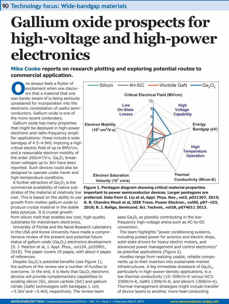
that might be deployed in high-powerelectronic and radio-frequency ampli-fier applications: these include a widebandgap of 4.5–4.9eV, implying a highcritical electric field of up to 8MV/cm,and a reasonable electron mobility ofthe order 200cm2/V-s. Ga2O3 break-down voltages up to 3kV have beenreported. Such devices could also bedesigned to operate under harsh andhigh-temperature conditions. A further attraction of Ga2O3 is the
commercial availability of native sub-strates of the material at relatively lowcost. This is based on the ability to usegrowth from molten gallium oxide toproduce crystal material in the stablebeta polytype. It is crystal growthfrom silicon melt that enables low cost, high-qualitysubstrates for mainstream electronics.University of Florida and the Naval Research Laboratory
in the USA and Korea University have made a compre-hensive review of the present and potential future status of gallium oxide (Ga2O3) electronics development[S. J. Pearton et al, J. Appl. Phys., vol124, p220901,2018]. The paper covers 19 pages, with about 4 pagesof references. Despite Ga2O3’s potential benefits (see Figure 1),
the authors of the review see a number of hurdles toovercome. In the end, it is likely that Ga2O3 electronicdevices will provide complementary capabilities toexisting silicon (Si), silicon carbide (SiC) and galliumnitride (GaN) technologies with bandgaps 1.1eV,~3.3eV and ~3.4eV, respectively. The review team
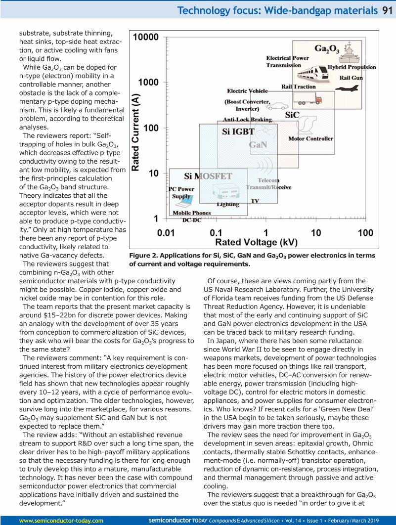
sees Ga2O3 as possibly contributing in the low-frequency high-voltage arena such as AC-to-DC conversion.The team highlights “power conditioning systems,
including pulsed power for avionics and electric ships,solid-state drivers for heavy electric motors, andadvanced power management and control electronics”as potential applications (Figure 2). Hurdles range from realizing usable, reliable compo-
nents up to their insertion into sustainable marketinfrastructures. A big immediate drawback of Ga2O3,particularly in high-power-density applications, is a low thermal conductivity (10–30W/m-K versus SiC’s330W/m-K, GaN’s 130W/m-K, and silicon’s 130W/m-K).Thermal management strategies might include transferof device layers to another, more heat-conducting
Figure 1. Pentagon diagram showing critical material propertiesimportant to power semiconductor devices. Larger pentagons arepreferred. Data from G. Liu et al, Appl. Phys. Rev., vol2, p021307, 2015;G. R. Chandra Mouli et al, IEEE Trans. Power Electron., vol50, p97–103,2018; B. J. Baliga, Semicond. Sci. Technol., vol28, p074011 2013.
Mike Cooke reports on research plotting and exploring potential routes tocommercial application.
Gallium oxide prospects forhigh-voltage and high-powerelectronics
Technology focus: Wide-bandgap materials
www.semiconductor-today.com semiconductorTODAY Compounds&AdvancedSilicon • Vol. 14 • Issue 1 • February/March 2019
91
substrate, substrate thinning,heat sinks, top-side heat extrac-tion, or active cooling with fans or liquid flow.While Ga2O3 can be doped for
n-type (electron) mobility in acontrollable manner, anotherobstacle is the lack of a comple-mentary p-type doping mecha-nism. This is likely a fundamentalproblem, according to theoreticalanalyses. The reviewers report: “Self-
trapping of holes in bulk Ga2O3,which decreases effective p-typeconductivity owing to the result-ant low mobility, is expected fromthe first-principles calculation of the Ga2O3 band structure. Theory indicates that all theacceptor dopants result in deepacceptor levels, which were not able to produce p-type conductiv-ity.” Only at high temperature hasthere been any report of p-typeconductivity, likely related tonative Ga-vacancy defects.The reviewers suggest that
combining n-Ga2O3 with othersemiconductor materials with p-type conductivitymight be possible. Copper iodide, copper oxide andnickel oxide may be in contention for this role. The team reports that the present market capacity is
around $15–22bn for discrete power devices. Makingan analogy with the development of over 35 yearsfrom conception to commercialization of SiC devices,they ask who will bear the costs for Ga2O3’s progress tothe same state? The reviewers comment: “A key requirement is con-
tinued interest from military electronics developmentagencies. The history of the power electronics devicefield has shown that new technologies appear roughlyevery 10–12 years, with a cycle of performance evolu-tion and optimization. The older technologies, however,survive long into the marketplace, for various reasons.Ga2O3 may supplement SiC and GaN but is notexpected to replace them.” The review adds: “Without an established revenue
stream to support R&D over such a long time span, theclear driver has to be high-payoff military applicationsso that the necessary funding is there for long enoughto truly develop this into a mature, manufacturabletechnology. It has never been the case with compoundsemiconductor power electronics that commercialapplications have initially driven and sustained thedevelopment.”
Of course, these are views coming partly from the US Naval Research Laboratory. Further, the Universityof Florida team receives funding from the US DefenseThreat Reduction Agency. However, it is undeniablethat most of the early and continuing support of SiCand GaN power electronics development in the USAcan be traced back to military research funding. In Japan, where there has been some reluctance
since World War II to be seen to engage directly inweapons markets, development of power technologieshas been more focused on things like rail transport,electric motor vehicles, DC–AC conversion for renew-able energy, power transmission (including high-voltage DC), control for electric motors in domesticappliances, and power supplies for consumer electron-ics. Who knows? If recent calls for a ‘Green New Deal’in the USA begin to be taken seriously, maybe thesedrivers may gain more traction there too. The review sees the need for improvement in Ga2O3
development in seven areas: epitaxial growth, Ohmiccontacts, thermally stable Schottky contacts, enhance-ment-mode (i.e. normally-off) transistor operation,reduction of dynamic on-resistance, process integration,and thermal management through passive and activecooling. The reviewers suggest that a breakthrough for Ga2O3
over the status quo is needed “in order to give it at
Figure 2. Applications for Si, SiC, GaN and Ga2O3 power electronics in termsof current and voltage requirements.
Technology focus: Wide-bandgap materials
semiconductorTODAY Compounds&AdvancedSilicon • Vol. 14 • Issue 1 • February/March 2019 www.semiconductor-today.com
92
least one application which will motivate R&D in theyears to come.”
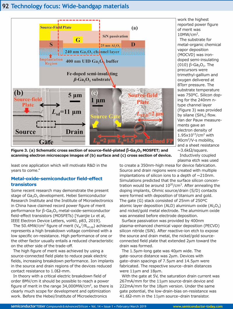
Metal-oxide-semiconductor field-effecttransistorsSome recent research may demonstrate the presentstage of Ga2O3 development. Hebei SemiconductorResearch Institute and the Institute of Microelectronicsin China have claimed record power figure of meritperformance for β-Ga2O3 metal-oxide-semiconductorfield-effect transistors (MOSFETs) [Yuanjie Lv et al,IEEE Electron Device Letters, vol40, p83, 2019].The 50.4MW/cm2 figure of merit (Vbr
2/Ron,sp) achievedrepresents a high breakdown voltage combined with alow specific on-resistance. High performance of one orthe other factor usually entails a reduced characteristicon the other side of the trade-off. The high figure of merit was achieved by using a
source-connected field plate to reduce peak electricfields, increasing breakdown performance. Ion implantsin the source and drain regions of the devices reducedcontact resistance to 1.0Ω-mm.In theory with a critical electric breakdown field of
order 8MV/cm it should be possible to reach a powerfigure of merit in the range 34,000MW/cm2, so there isclearly much scope for development and optimizationwork. Before the Hebei/Institute of Microelectronics
work the highestreported power figureof merit was10MW/cm2.The substrate for
metal-organic chemicalvapor deposition(MOCVD) was iron-doped semi-insulating(010) β-Ga2O3. Theprecursors weretrimethyl-gallium andoxygen delivered at8Torr pressure. Thesubstrate temperaturewas 750ºC. Silicon dop-ing for the 240nm n-type channel layer(Figure 3) was providedby silane (SiH4) flow.Van der Pauw measure-ments gave an electron density of1.95x1013/cm2 with90cm2/V-s mobility, and a sheet resistance~3.6kΩ/square. Inductively coupled
plasma etch was usedto create a 350nm-high mesa for device fabrication.Source and drain regions were created with multipleimplantations of silicon ions to a depth of ~210nm.Simulations predicted that the surface silicon concen-tration would be around 1020/cm3. After annealing thedoping implants, Ohmic source/drain (S/D) contactswere formed with deposition of titanium and gold. The gate (G) stack consisted of 25nm of 250ºC atomic layer deposition (ALD) aluminium oxide (Al2O3)and nickel/gold metal electrode. The aluminium oxidewas annealed before electrode deposition.Surface passivation was provided by 400nm
plasma-enhanced chemical vapor deposition (PECVD)silicon nitride (SiN). After reactive-ion etch to exposethe source and drain metal, the nickel/gold source-connected field plate that extended 2μm toward thedrain was formed.The 1.5μm-long gate was 40μm wide. The
gate–source distance was 2μm. Devices withgate–drain spacings of 7.5μm and 14.5μm were fabricated. The respective source–drain distances were 11μm and 18μm.With the gate at 5V, the saturation drain current was
267mA/mm for the 11μm source-drain device and222mA/mm for the 18μm version. Under the samegate potential, the low-drain-bias on-resistance was41.6Ω-mm in the 11μm source–drain transistor.
Figure 3. (a) Schematic cross section of source-field-plated β-Ga2O3 MOSFET; andscanning electron microscope images of (b) surface and (c) cross section of device.
Technology focus: Wide-bandgap materials
www.semiconductor-today.com semiconductorTODAY Compounds&AdvancedSilicon • Vol. 14 • Issue 1 • February/March 2019
93
With 20V drain bias, the maximum transconductancefor the 11μm MOSFET was 10.5mS/mm. The0.1mA/mm threshold gate voltage was at 50.5V. Gate leakage was around 7.1x10⁻⁷A/mm. Theresearchers see this value as being “comparatively
large”, adding that the culprit may be Al2O3/Ga2O3
interface traps. They suggest that these traps could bereduced with a better optimized surface-state treatment.Further evidence of interface traps was given by ~0.8Vhysteresis in the response under forward and reversesweeps of gate voltage. The on/off current ratio was ofthe order 106. Destructive breakdown performance in air was
carried out with the gate at –55V (see Figure 4). With-out source field plates, the breakdown voltages were310V and 260V for the 18μm and 11μm MOSFETs,respectively. These values were greater than the 218Vvalue expected from a one-sided abrupt-junction model.The researchers suggest the better-than-theory resultas being due to non-uniformity of channel doping and depletion from interface states. Adding source field plates increased the breakdown to 480V in the11μm device and 680V in the 18μm MOSFET.Multiplying the on-resistance by the source–drain
distance to give Ron,sp, the researchers found values of4.58mΩ-cm2 and 11.7mΩ-cm2 for the 11μm and18μm devices, respectively. “Our fabricated devices inthis work show much lower Ron,sp compared with otherβ-Ga2O3 MOSFETs and also with the theoretical per-formance of Si-based power devices,” the team com-ments.Although the saturation drain current is still lower
than in reported nanomembrane Ga2O3 devices, theresearchers claim that their source-field-plated MOSFETshows a record maximum drain current and power
Figure 4. Three-terminal off-state breakdowncharacteristics of β-Ga2O3 MOSFET with and withoutsource-field plate for (a) 11μm and (b) 18μmsource–drain distance devices. (c) Plot of Ron,sp
versus Vbr for Hebei/Institute of Microelectronicsdevices (“this work”) and other reported lateralGa2O3 MOSFETs.
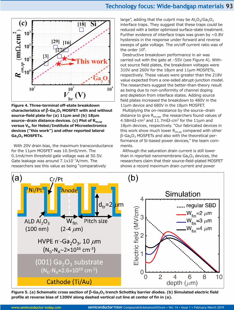
Figure 5. (a) Schematic cross section of β-Ga2O3 trench Schottky barrier diodes. (b) Simulated electric fieldprofile at reverse bias of 1200V along dashed vertical cut line at center of fin in (a).
Technology focus: Wide-bandgap materials
semiconductorTODAY Compounds&AdvancedSilicon • Vol. 14 • Issue 1 • February/March 2019 www.semiconductor-today.com
94
figure of merit among devices fabricated on homo-epitaxial β-Ga2O3. The researchers suggest thatincreasing the channel layer thickness in conjunctionwith gate recessing could lead to lower on-resistanceand associated improvement in the power figure ofmerit.
Schottky barrier diodesCornell University in the USA and Novel Crystal Tech-nology Inc in Japan claim the lowest leakage current yetreported for β-Ga2O3 Schottky barrier diodes (SBDs),another key device type for power applications [Wen-shen Li et al, Appl. Phys. Lett., vol113, p202101, 2018].The low leakage current density of less than 1μA/cm2
was combined with a relatively high breakdown voltageof 1232V. The devices used a trench structure to createfins with a metal-insulator-semiconductor (MIS) stackon the sidewalls to reduce surface field effects, sup-pressing leakage under reverse bias. The researchers used halide vapor phase epitaxy
(HVPE) to create the device layers of the SBD (Figure 5).The fin area ratio was ~60% of the total fin+trench pitch.In simulations, a narrower fin was expected to result inlower electric fields near the top surface. The 10μmdrift layer had a uniform net doping of 2x10¹⁶/cm3
that made a significant contribution to the improvedperformance.Fabrication began with formation of the back cathode:
first reactive ion etch (RIE) was performed to improvethe ohmic nature of the contact, followed by evaporationand annealing of the titanium/gold (Ti/Au) contact metal.
The front-side of the epitaxial wafer was patterned,using nickel/platinum (Ni/Pt) as both the hard mask for trench RIE etching and the Schottky contact of thefinal device. The trenches were etched to a depth of2μm with the fin channels oriented along the [010]direction. The fin sidewalls are described as being ‘near vertical’. The trenches were lined with atomic layer deposition
Al2O3. Dry etch through the Al2O3 at the tops of the fins exposed the nickel/platinum Schottky contacts.The device was completed with sputteringchromium/platinum (Cr/Pt) on the trench sidewalls.The researchers also produced Ni/Pt Schottky diodes
without the fin structuring, for comparison. The currentdensities were calculated based on device, not fin,area. The ideality factor of both devices was 1.08. Thetrench SBDs had a Schottky barrier height of 1.40eV,compared with 1.35eV for the regular device. Theincreased effective barrier height was attributed to theadjacent metal-oxide-semiconductor junction on thesidewalls of the trenches.Pulsed measurements were used to avoid self-heating
effects. The restricted area of the current flow throughthe fins resulted in reduced current density comparedwith the regular device. The specific differential on-resistance of the trench SBD was 15mΩ-cm2, compared with 6.6mΩ-cm2 for the regular device. The trench SBD also suffered from trapping effects
in voltage scans not seen in the regular device. Theresearchers infer that “the trapping must be located atthe trench MIS structure”. The trapped charge increases
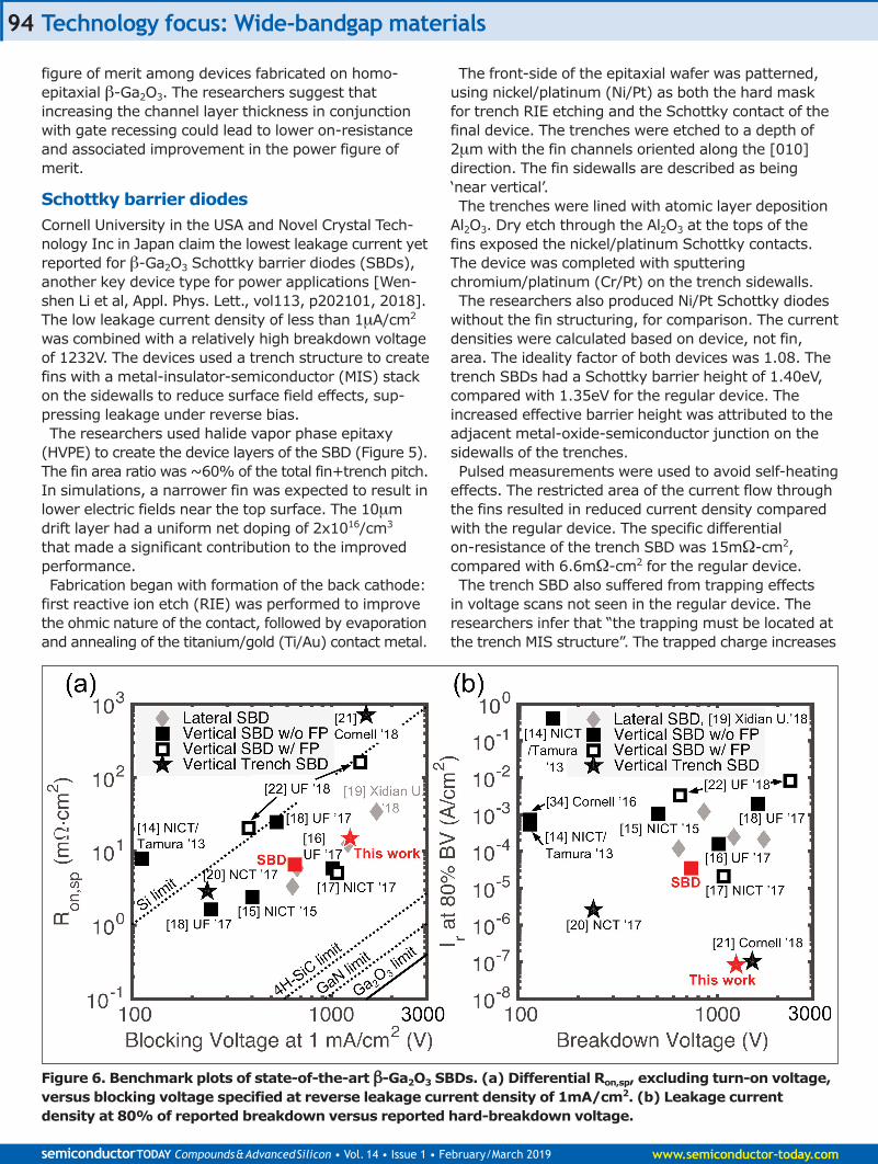
Figure 6. Benchmark plots of state-of-the-art β-Ga2O3 SBDs. (a) Differential Ron,sp, excluding turn-on voltage,versus blocking voltage specified at reverse leakage current density of 1mA/cm2. (b) Leakage currentdensity at 80% of reported breakdown versus reported hard-breakdown voltage.

the depletion in the fin, constricting current flow. Theresearchers estimate the extra depletion thickness tobe of the order 170nm at zero bias, assuming atrapped electron sheet density of ~8x10¹¹/cm2.The team suggests that the trapping could be
reduced with a post-deposition anneal (PDA) of theAl2O3 dielectric and with improved surface treatmenton the Ga2O3 surface after the dry etch.The place where the trench SBD performed better
was under reverse bias with breakdown at 1232V,compared with 734V for the regular device. The fins ofthe best trench SBD were 2μm wide. The leakage cur-rent before breakdown was less than 1μA/cm2, andwhen the reverse bias was below 1000V the leakagewas less than 0.1μA/cm2, corresponding to power dis-sipation less than 0.1mW/cm2. Wider finned deviceshad higher leakage and lower breakdown voltages.The team compared the performance of its devices
with other reports (Figure 6). The specific differentialon-resistance compared with the blocking voltage at1mA/cm2 current density showed ‘notable’ improvementover previously reported trench devices, while also
giving comparable performance to the best reported β-Ga2O3 SBDs. The team comments: “In comparisonwith our previous results, the on-resistance is muchreduced due to a more uniform doping profile with amoderate level (~2x10¹⁶/cm3) and less carrier com-pensation.” Comparison was also made between the reverse
leakage at 80% of breakdown and the breakdown volt-age itself, showing lower leakage in the trench SBDs,compared with regular devices. The researchers claimthe lowest leakage reported for the SBDs with 2μm-wide fins. The team’s regular SBD showed similar performance to other reports. The lower leakage istherefore likely attributable to the trench structureitself. The team expects progress toward the theoretical
material limit for Ga2O3 through reduced trapping inthe MIS structure and better field management. ■
The author Mike Cooke is a freelance technology journalistwho has worked in the semiconductor and advancedtechnology sectors since 1997.
Technology focus: Wide-bandgap materials
www.semiconductor-today.com semiconductorTODAY Compounds&AdvancedSilicon • Vol. 14 • Issue 1 • February/March 2019
95
REGISTERfor Semiconductor Today
free at www.semiconductor-today.com


![Band alignment of Al2O3 with (-201) β-Ga2O3ww2.che.ufl.edu/ren/paper/2017 p27.pdf · Chemical Vapor Deposition (MOCVD) have been reported [1e13]. The large bandgap of Ga2O3 means](https://img.pdfslide.us/doc/110x75/5e8806a2765f02041f4fdbf2/band-alignment-of-al2o3-with-201-p27pdf-chemical-vapor-deposition-mocvd.jpg)