Embed Size (px)
Citation preview

Energy Research and Development Div is ion FINAL PROJECT REPORT
ADVANCED EPI TOOLS FOR GALLIUM NITRIDE LIGHT EMITTING DIODE DEVICES
DECEMBER 2012CEC ‐500 ‐2013 ‐027
Prepared for: California Energy Commission Prepared by: Applied Materials, Inc.

Prepared by: Primary Author(s): Nag Patibandla, Ph.D. Applied Materials, Inc. 3050 Bowers Avenue P. O. Box 58039 Santa Clara, CA 95054-3299 408-563-5224 Contract Number: PIR-10-055 Prepared for: California Energy Commission Dustin Davis Contract Manager Virginia Lew Office Manager Energy Efficiency Research Office Laurie ten Hope Deputy Director ENERGY RESEARCH AND DEVELOPMENT DIVISION Robert P. Oglesby Executive Director
DISCLAIMER This report was prepared as the result of work sponsored by the California Energy Commission. It does not necessarily represent the views of the Energy Commission, its employees or the State of California. The Energy Commission, the State of California, its employees, contractors and subcontractors make no warranty, express or implied, and assume no legal liability for the information in this report; nor does any party represent that the uses of this information will not infringe upon privately owned rights. This report has not been approved or disapproved by the California Energy Commission nor has the California Energy Commission passed upon the accuracy or adequacy of the information in this report.

1
ACKNOWLEDGEMENTS
This material is based upon work supported by the United States Department of Energy (DOE) under Award Number DE‐EE0003331 and by the California Energy Commission (Energy Commission), agreement PIR‐10‐055.
The project team gratefully acknowledges the hard work of the DOE and Energy Commission in developing and managing this important project. The project team extends thanks to project managers, Brian Dotson of DOE’s National Energy Technology Laboratory (NETL) and Dustin Davis of the Energy Commission, who helped guide this work.
Also, the project team thanks Jim Brodrick, the solid‐state lighting portfolio manager in DOEʹs Office of Energy Efficiency and Renewable Energy. His vision for solid state lighting and manufacturing were very helpful to successfully execute this project.
FINALLY, THE TEAM THANKS SEAN EVANS, WHO WAS THE INITIAL PROGRAM MANAGER AT NETL

2
PREFACE
The California Energy Commission Energy Research and Development Division supports public interest energy research and development that will help improve the quality of life in California by bringing environmentally safe, affordable, and reliable energy services and products to the marketplace.
The Energy Research and Development Division conducts public interest research, development, and demonstration (RD&D) projects to benefit California.
The Energy Research and Development Division strives to conduct the most promising public interest energy research by partnering with RD&D entities, including individuals, businesses, utilities, and public or private research institutions.
Energy Research and Development Division funding efforts are focused on the following RD&D program areas:
• Buildings End‐Use Energy Efficiency
• Energy Innovations Small Grants
• Energy‐Related Environmental Research
• Energy Systems Integration
• Environmentally Preferred Advanced Generation
• Industrial/Agricultural/Water End‐Use Energy Efficiency
• Renewable Energy Technologies
• Transportation
Advanced EPI Tools for Gallium Nitride Light Emitting Diode Devices is the final report for the grant, PIR‐10‐055, conducted by Applied Materials Incorporated. The information from this project contributes to Energy Research and Development Division’s Buildings End‐Use Energy Efficiency Program.
For more information about the Energy Research and Development Division, please visit the Energy Commission’s website at www.energy.ca.gov/research/ or contact the Energy Commission at 916‐327‐1551.

3
ABSTRACT
For light emitting diodes (LEDs) to realize its potential in lowering energy consumption and becoming the standard for general lighting needs, it is generally agreed that costs to the consumer must come down significantly. When Applied Materials Incorporated (Applied Materials) conducted a comprehensive review of the value chain of the LED bulb, it was clear that Gallium Nitride (GaN) deposition costs were a significant driver in the final cost of the bulb. The costs not only include tool cost, but the yield and performance of the chips out of the tool. The overall goal of this project was to develop, build, and demonstrate an improved manufacturing system for GaN power devices such as LEDs. Applied Materials designed, demonstrated and validated the system performance of the full LED Epitaxy (epi) process. The project accomplished its goals and resulted in successfully building a world‐class, epi system that produces high quality LEDs at a lower cost which is now commercially available. Keywords: LEDs, Light Emitting Diodes, Applied Materials, solid state lighting, GaN LED manufacturing
Please use the following citation for this report:
Patibandla, Nag (Applied Materials, Inc.). 2012. Advanced EPI Tools for Gallium Nitride Light Emitting Diode Device. California Energy Commission. Publication Number: CEC‐500‐2013‐027

4
TABLE OF CONTENTS
Acknowledgements .................................................................................................................................. 1
PREFACE .................................................................................................................................................... 2
ABSTRACT ................................................................................................................................................ 3
TABLE OF CONTENTS ........................................................................................................................... 4
EXECUTIVE SUMMARY ........................................................................................................................ 5
Introduction ............................................................................................................................................ 5
APPENDIX A: Applied Materials Report to U.S. Department of Energy .................................. A‐1

5
EXECUTIVE SUMMARY
Introduction The California Energy Commission (Energy Commission) provided cost share funding to supplement Applied Materials, Incorporated’s (Applied Materials) American Recovery and Reinvestment Act of 2009 (ARRA) award. The purpose of the project was to conduct research and development of a new, more cost effective process for manufacturing Gallium Nitride (GaN) power devices such as Light Emitting Diodes (LEDs). The Energy Commission’s cost share assisted in the design and development of a new method to produce high quality light emitting diodes at a lower cost.
The project resulted in the demonstration of a prototype tool that can deposit high‐quality GaN materials on at least two different substrate materials. This new advanced system will enable LED manufacturers to fabricate higher‐quality LED devices at a lower cost, and help address a major obstacle to widespread adoption of high quality and more energy efficient LEDs. This project accomplished the goals of designing, validating and developing improved GaN manufacturing process equipment that is now commercially available.
Wide spread adoption of LEDs could significantly reduce energy use associated with lighting. The LED technology is an efficient light source over other technologies such as incandescent. Incandescent lighting produces up to 18 lumens of light output for every watt of energy it consumes while LEDs produce up to 100 lumens for every watt.
Energy Commission funding was critical to retain jobs during a down economy at Applied Materials’ Research and Development facility in Santa Clara, California. By 2015, Applied Materials estimates that 350 employees will be assigned to the product that resulted from this project. About one‐half of the employees will be in Santa Clara, California. These employees will work in engineering, manufacturing, service and maintenance, technology, marketing, administration, and critical support functions such as finance, human resources, and legal counsel.
Appendix A contains a copy of the final report, Advanced Epi Tools for Gallium Nitride Light Emitting Diode Devices, prepared by Applied Materials for the U. S. Department of Energy under grant DE – EE0003331.

A‐1
APPENDIX A: Applied Materials Report to U.S. Department of Energy Submitted to the U. S. Department of Energy, Agreement DE‐EE0003331, December 7, 2012

Solid
Adv Nitri
Wo
PrincipaP
E-M
PrP
E-M
NatioPro
E-
State LFINAL
Decem
vanced Epde Light E
ork PerformDE-
SubApplied
3050 BP.O
Santa Clar
al InvestigaPhone Num
Fax NumbMail: nag_p
ogram ManPhone NumMail: vivek
Sub
U. S. Depaonal Energy oject Officer-Mail: Brian.
LightingL REPO
mber 7, 201
pi Tools foEmitting D
med Under A
EE0003331
bmitted By:d Materials, Bowers Aven
. Box 58039ra, CA 9505
tor: Nag Paber: (408) 5
ber: (408) 56patibandla@
nager: Vivekber: (408) 5
k_agrawal@
bmitted To:
artment of ETechnology
r: Brian DotDotson@NET
g ProgrORT
12
or GalliumDiode Dev
Agreement: 1
Inc.
nue 9 54-3299
atibandla, P563-5224 63-6311 @amat.com
k Agrawal563-1368
@amat.com
Energy y Laboratortson, Ph. D.
TL.DOE.GOV
ram
m vices
Ph.D.
ry .

2
2
Disclaimer:
This report was prepared as an account of work sponsored by an agency of the United States Government. Neither the United States Government nor any agency thereof, nor any of their employees, makes any warranty, express or implied, or assumes any legal liability or responsibility for the accuracy, completeness, or usefulness of any information, apparatus, product, or process disclosed, or represents that its use would not infringe privately owned rights. Reference herein to any specific commercial product, process, or service by trade name, trademark, manufacturer, or otherwise does not necessarily constitute or imply its endorsement, recommendation, or favoring by the United States Government or any agency thereof. The views and opinions of authors expressed herein do not necessarily state or reflect those of the United States Government or any agency thereof."

3
3
ContentsExecutiveSummary..............................................................................................................................4
ProgramGoalsandAccomplishments...........................................................................................5
Overview ................................................................................................................................. 5
Program Goals ........................................................................................................................ 5
ProjectActivitySummary.................................................................................................................27
Original hypotheses .............................................................................................................. 27
Approaches used ................................................................................................................... 29
Problems encountered ........................................................................................................... 30
Productsdevelopedundertheaward.........................................................................................31
Networks or collaborations fostered ..................................................................................... 31
Technologies/Techniques ..................................................................................................... 31
Inventions/Patent Applications ............................................................................................. 31
Summary................................................................................................................................................32
Acknowledgements............................................................................................................................33

4
ExecutiveSummary
Over the course of this program, Applied Materials, Inc., with generous support from the United States Department of Energy, developed a world-class three chamber III-Nitride epi cluster tool for low-cost, high volume GaN growth for the solid state lighting industry. One of the major achievements of the program was to design, build, and demonstrate the world’s largest wafer capacity HVPE chamber suitable for repeatable high volume III-Nitride template and device manufacturing. Applied Materials’ experience in developing deposition chambers for the silicon chip industry over many decades resulted in many orders of magnitude reductions in the price of transistors. That experience and understanding was used in developing this GaN epi deposition tool. The multi-chamber approach, which continues to be unique in the ability of the each chamber to deposit a section of the full device structure, unlike other cluster tools, allows for extreme flexibility in the manufacturing process. This robust architecture is suitable for not just the LED industry, but GaN power devices as well, both horizontal and vertical designs. The new HVPE technology developed allows GaN to be grown at a rate unheard of with MOCVD, up to 20x the typical MOCVD rates of 3m per hour, with bulk crystal quality better than the highest-quality commercial GaN films grown by MOCVD at a much cheaper overall cost. This is a unique development as the HVPE process has been known for decades, but never successfully commercially developed for high volume manufacturing. This research shows the potential of the first commercial-grade HVPE chamber, an elusive goal for III-V researchers and those wanting to capitalize on the promise of HVPE. Additionally, in the course of this program, Applied Materials built two MOCVD chambers, in addition to the HVPE chamber, and a robot that moves wafers between them. The MOCVD chambers demonstrated industry-leading wavelength yield for GaN based LED wafers and industry-leading uptime enabled in part by a novel in-situ cleaning process developed in this program. The Department of Energy was a great supporter of this leading-edge technology that can benefit U.S. industry and keep GaN manufacturing competitive in the United States. We gratefully acknowledge their role in advancing the state-of-the-art.

5
ProgramGoalsandAccomplishments
Overview For solid state lighting to realize its potential in lowering energy consumption for the nation and becoming the standard for general lighting needs, it is generally agreed that costs to the consumer must come down significantly. When Applied Materials did a comprehensive review of the value chain of the LED bulb, it was clear that GaN deposition costs were a significant driver in the final cost of the bulb. The costs not only include tool cost, but the yield and performance of the chips out of the tool. The overall goal of this program was to develop, build, and demonstrate a low-cost manufacturing system for GaN LED manufacturing. Not only did we design a system, but validate the system by developing a full LED epi process. We set this high bar of actually demonstrating world-class device performance because of the reputation Applied Materials has built over many decades as the leader in high volume nano-scale manufacturing. Without developing a process, and given the fact that Applied Materials was new to this market, we could not validate the world-class nature of our system. We are happy to report that we accomplished the goals we set out to accomplish in this successful program, building a world-class, low-cost epi system for GaN LEDs that has shipped to customers world-wide. We describe our achievements in more detail below. Our approach was fundamentally different than the standard approach in two ways. First, Applied Materials would use the cluster approach that it has successfully implemented in the silicon industry, driving down manufacturing costs by orders of magnitude and enabling the information age. Secondly, we would develop the world’s first manufacturing-grade HVPE chamber to increase the rate of GaN deposition by over an order of magnitude, further driving down epi manufacturing costs for the LED industry.
ProgramGoals There were five milestones proposed at the start of this program in 2010. We are happy to report that we exceeded expectations for all of them. This program was unique in that Applied Materials not only designed new epi chamber architectures, but developed GaN process and GaN devices to show the viability of the tool design. This feedback loop was a key to the success of the program and sometimes not recognized as a necessary requirement. The key achievements for each milestone are highlighted below.

6
Mileston
GoalIncrease phase epias an MO
AccomplTable 1 scapacity with oper
Key adva
1. F2. U3. E
fo4. E
X5. S6. Im7. L8. P
le9. P
ne1:Multi‐
manufacturiitaxy (HVPE
OCVD system
lishmentssummarizes HVPE chamrating costs
ancements in
ast GaN depUnique in-situExcellent u-Gor (002) of 9
Excellent u-GXRD FWHM
mooth GaN mprovement
Lower defectrocess flexib
evels roduction H
waferHVPE
ing throughpE) system thm.
the achievemmber that wasignificantly
Table
n the proprie
position ratesu HVPE buf
GaN/n-GaN c90-130” and GaN/n-GaN c
M for (002) omorphology
t of light extr densities fobility for wid
HVPE tool wi
EEpiCham
put by develoat can depos
ments in dess demonstra
y below MO
e 1: Summary
etary Applied
s for high thrffer techniqucrystalline q(102) of 200crystalline qf 170” and (y raction
or IQE, leakade range of u
ith high capa
mber
oping and assit high-qual
igning and bated to grow CVD.
y of HVPE Acc
d Materials H
roughput anues for GaN quality on pla0-250” quality on pa102) of 150”
age current imu- and n-GaN
acity : 31 x 2
ssembling a lity GaN wit
building the thick GaN l
complishment
HVPE techn
nd productivideposition oanar sapphir
atterned sapp”
mprovementN thicknesse
2”, 8 x 4”, 4
multi-waferth a growth r
world’s largayers of exc
ts
nology inclu
ity on planar sapre wafers wit
phire substra
t es, and high
x 6”, 1 x 8”
r hydride vaprate twice as
gest wafer ceptional qua
de:
pphire and Pth XRD FW
ate (PSS) wit
Si n-doping
”
por fast
ality
PSS WHM
th
g

7
GaNTh The finalafter inveachievedwafers anvariationuniformitpockets a1.2%, 1-
Figure within-p
GaNCry
Optimizamaterial repeatabiproprietaproductio
icknessUn
l HVPE chamestigating m
d with our finnd we report
ns from the cty maps for across the ca.
1: 4-wafer radlatter (WiP) w
ystallineQ
ation of the Hwith excelleility of GaN ary in-situ HVon worthines
niformity.
mber design any differen
nal design. Tt a radial 1-enter of the GaN layers
arrier are sho
dial thicknessweighted unifo
uality
HVPE in-situent crystallin
crystal qualVPE buffer ss of the HV
and processnt options. FiThe carrier in uniformitychamber outgrown on fo
own in Figur
uniformity dormity 1-σ her
u buffer techne quality onlity (XRD RCon planar 2 i
VPE chamber
s gas deliverigure 1 shown the chambey of 1.4%. Ttward, which
our 2 inch plare 1. Within
ata based on are is 1.4%; wh
hniques gaven planar sappC FWHM) finch sapphirr. The total t
ry systems wws the GaN ter accommo
The design ofh were optimanar sapphirwafer thickn
a HVPE GaN hile average w
e us the oppophire. Fig. 2 for u-/n-GaNre substratesthickness of
was chosen anthickness unidated 31 twof the chambemized. The thre substratesness uniform
run on a 31×2within-wafer (W
ortunity to gshows excel
N structure g. This is evidthe u-/n-GaN
nd optimizediformity thato inch sappher led to radihickness located in f
mity is within
2-in carrier. TWiW) 1-σ is 1
grow GaN llent run-to-r
grown with dence of theN structure i
d t was hire ial
four n
The .2%.
run
e is 7

8
m (the tatom/cm
Figure 2buffer on
thickness of 3).
2: HVPE GaNn planar 2 inch
f n-GaN is ab
N XRD RC FWh sapphire sub
cleaning
bout 3.5m
WHM for 7 mbstrates in 14 recipe was ap
with doping
m thick u-/n-Grepeatable de
pplied after ea
g carrier conc
GaN structure eposition runsach deposition
centration of
grown with ps. The in-situ C run.
f 5E18
roprietary in-Cl2 based cham
-situ mber

9
Mileston
GoalDecreaseHVPE+Mquantum each waf
Accompl
DeviceP Validatiothe advanmanufactthe LED in additio Figures 3chamber clearly shVolume M
ne2:HVPE
e cycle time MOCVD sys
efficiency ofer and wafer
lishments
Performan
on of our epinced design turers wouldindustry, ou
on to high vo
3 and 4 showtool with pe
howing the cManufacturi
Figure 3: 8
andMOCVD
and improvestem and a mof 75% and (r-to-wafer.
ce.
itaxial tool aof the chamb
d not have reur customersolume, produ
w the quality erformance ocapability using.
88% IQE Dem
DDeviceIn
e binning yiemanufacturin(b) PL wavel
architecture rbers. This w
equired. How required thauction-worth
of LED’s abof 88% IQE sing the epi e
monstrated on
tegration
eld by demonng process thlength unifo
required devwas a challenwever, becauat we demonhy chambers
ble to be achand 57% EQ
equipment d
LEDs from th
nstrating a thhat can produormity variat
veloping wornge that otheruse we were nstrate worlds.
hieved in theQE, among tdeveloped un
he Applied Ma
hree-chambeuce LEDs wition of < 1.5n
rld-class LEDr GaN epi chnot an estab
d-class devic
e Applied Mthe best in thnder this prog
aterials Cluste
er MOCVD ith (a) internnm, 1σ with
D’s in additihamber
blished playince performan
aterials multhe industry, gram for Hig
er Tool
/ nal hin
ion to
ng in nce
ti-
gh

10
Hands‐O High-volassistancoff” operMOCVDachievem Hands of“to be prthey wereremainedprocessedproceedeof the chtwo actio
Figure 4: 57
Off120 Con
lume produce from an op
ration of the D, starting wiment.
ff means thatocessed” wae processed.
d closed durid 60 runs in
ed to run 120ambers in ad
ons resulted i
7% EQE Dem
nsecutiveR
ction requiresperator, techLED epi sysith 10 runs a
t the only tasafers on the a There were
ing the entirehands off m
0 additional hddition to thein the perfor
monstrated on
Runs
s tools that chnician or prostem being d
and ending w
sk for the opautomated we no recipe ae proceeding
mode, performhands-off rue in-situ clearmance show
LEDs from th
can perform ocess enginedeveloped unwith the hand
perator was twafer loadingadjustments gs. As can bmed an 8 houuns. This wasan process, Mwn.
he Applied M
the requiredeer. A key mnder this prods-off mode
to place the wg mechanismor tweaks al
be seen in Figur periodic ms accomplishMilestone 4.
Materials Clust
d task(s) withmeasurementogram was aat 120 runs,
wafer cassetm and then rellowed and tgure 5, we fmaintenancehed by desig The combi
er Tool
h minimum t of the “hanccomplished, a significan
tte holding themove them the chamber first successfe and then gn improvemination of the
nd-d in nt
he after
fully
ments ese

11
Figure 5: Awavelengt The handsystems aseasoningvarious M HighQu Another flow andlayer whiof the sys
A key achieveth uniformity
ds-off 12- coand the frequg, and epi re
Milestones th
ualityMQW
major resulttemperature
ich is controstem with fa
ement of the pand no openin
onsecutive ruuent intervenecipe adjustmhroughout th
W
t of the multie control durolled by bothast response r
Figure 6
rogram: 60 anng of the cham
uns is a majontion for ma
ments. This he program.
i-chamber prring MQW gh gas flows aradiant heati
6: MQW SEM
nd 120 continumber.
or improvemanual cleanincapability w
rogressive pgrowth. Figuand ultra-preing is creatin
M cross section
uous “hands-o
ment over theng, parts replwas a signific
process is theure 6 shows
ecise thermalng strong res
n and periodi
off” runs with
e operation olacement, chcant factor in
e precision bthe consiste
l control. Thsults for MQ
city
h exceptional
of conventionhamber n reaching
brought to thency in the Mhe configuratQW consisten
nal
he gas MQW tion ncy.

12
PLResu Figure 7 examine nm bin arfor LED min-max
ults
shows the wcumulative round the tarmanufacture
x variation of
wavelength uPL performargeted 450nmers. Figure 8f 12.5nm.
Figu
uniformity france. The rem value, cle
8 shows the w
ure 7: Distribu
rom a series esults showe
early demonswavelength u
ution of PL fo
of runs withed 86.9% of strating exceuniformity w
or Wavelength
h a number oall points w
eptional binnwithin a sing
h
of wafers to were located ining capabiligle carrier an
in a 5 ities nd a

13
Fig Bow
Typicallywafer benduring gris especiaMOCVDInGaN M
In order ton waveltemperatu
The stresmanagedbow wastemperatusitu opticmultiple profile acGaN/n-G
gure 8: Full ca
y, lattice misnding, defecrowth is the ally importan
D growth is kMQW growth
to verify thelength uniforure bow for
ss during HVd by changin
also managure convex bcal bow meaquantum wecross the 2”
GaN templat
arrier mappin
smatch and tct formation,change of thnt for indium
known to be h conditions
impact of wrmity, we ussubsequent
VPE growth g of HVPE ped by changbow height wsurements at
ell test structwafer for Intes.
ng of waveleng
thermally ind, or even filmhermal contam-containingvery temperis required f
wafer curvatused HVPE u-MOCVD In
(and as a resprocess para
ging of u-GaNwas used- 8 t room tempture growth.
nGaN multip
gth showing ex
duced stress m cracking. Aact between tg compoundrature sensitifor good in w
ure during ou-GaN/n-GaN
nGaN multip
sult, the bowameters durinN/n-GaN thto 60 m. Th
perature and Table 2 shole quantum w
xceptional mi
during MOCAn importanthe wafer ans, since indiuive. Therefowafer wavel
ur HVPE+MN templates wple quantum
w of u-GaN/nng in-situ buhickness andhe templatestransferred t
ows the PL mwell structur
in-max binnin
CVD LED gnt impact of nd the substrum incorpor
ore, wafer bolength unifor
MOCVD intewith differenwell structur
n-GaN tempuffer steps. Ind a range of rs were charato the MOCV
mapping andres grown on
ng of 12.5nm
growth resulwafer bendiate holder. Tration duringow control atrmity.
egration grownt room re growth.
plates) was n some runsroom acterized by VD chamber
d wavelengthn HVPE u-
lts in ing This g t
wth
s the
ex r for
h line

14
Table 2: Pwell struct
Three HVsubsequetemplatesbow (9 STD (3.5result, th The conscenter) caAssuminInGaN Mwavelengacross th So, with distributiuniformit
To verifyMOCVDwere placdepositioHVPE testructurewaveleng
PL mapping antures grown o
VPE u-GaN/ent InGaN ms revealed dim) template57 nm) the we wavelengt
siderable conan be correla
ng that the waMQW growthgth profile cae wafer) at I
stress controion across thty.
y the w-to-wD runs was coced on 31x2
on in HVPE emplates (locs were depogth uniformi
nd wavelengthon HVPE u-Ga
/n-GaN tempmultiple quan
ifferent behae exhibits a cwavelength p
h STD is low
ncave waveleated to the cafer center ih conditions)an be correlaInGaN MQW
ol during HVhe wafer duri
w and run-to-onducted in ” carrier andchamber at ocated across sited in MOity data for th
h profile acrosaN/n-GaN tem
plates had dintum well stravior in termconsiderableprofile for higw (0.95 nm)
ength profileonvex wafers cooler than) a higher inated to a flat
W growth co
VPE growth,ing MOCVD
run wavelenAMAT clus
d transferredoptimized (fthe carrier) wCVD chambhree MOCV
ss the 2” sappmplates
ifferent convructure depo
ms of wavelen concave wagh convex bfor this tem
e (or red shifr shape at Inn the wafer e
ndium concent wafer shapenditions.
, we were abD GaInN MQ
ngth uniformster tool. Sixd to HVPE chfor stress conwas transfer
ber and charaVD runs are p
hire substrate
vex bow heigosition on thength uniformavelength prbow (51 m)
mplate.
ft of the PL nGaN MQW edges in the ntration can e (and unifo
ble to optimiQW growth a
mity asequencx 2 inch sapphamber. Aftentrol) conditrred to MOCacterized bypresented at
e for InGaN m
ght: 9, 26 ane top of HVPmity. While tofile and hig
) template is
wavelength growth concase of convbe expectedrm temperat
ize the tempeand achieve
ce of three Hphire substrater 6 m thictions, the carCVD chambey ex-situ PL.
Table 3.
multiple quant
nd 51 m. AfPE templatesthe low convgh wavelengnearly flat. A
in the waferditions. vex bowing d. The flat ture distribut
erature high wavele
HVPE and thtes for each
ck u-GaN/n-Grrier with sixer. The test LThe PL
tum
fter s, all vex
gth As a
r
(at
tion
ength
hree run GaN x LED

15
Table 3: The PL wavelength uniformity data from LED structures grown on HVPE u-GaN/n-GaN templates in three MOCVD runs
The average data for PL wavelength uniformity are presented at Table 4. The within wafer uniformity and run-to-run uniformity have achieved the target. The wafer-to-wafer uniformity is close to the target and can be improved by additional tuning.
Table 4:Average data for PL wavelength uniformity of integrated HVPE/MOCVD runs
A quick EL apparatus is used to measure the EL wavelength at 5 points across the wafer and the wavelength STD is calculated. Table 4 is an example of EL measurement of a wafer from the integrated HVPE/MOCVD run. It shows the EL STD of HVPE and MOCVD can achieve 1.15 nm which exceeds the target of 1.5 nm.
Table 5: EL and PL wavelength measurement
Run ID 6MA079 Run ID 6MA080 Run ID 6MA081
Waf
er
ID Wavelength
(nm) STD (nm)
Wavelength (nm)
STD (nm)
Wavelength (nm)
STD (nm)
2 448 1.11 446 1.23 447.9 1.58 14 445.6 1.05 444.7 1.22 445.8 1.42 25 445.5 1.32 444.1 1.6 444.1 1.9 27 444.8 1.16 444.8 1.68 444 1.93 17 446.4 1.13 445.9 1.08 444.6 1.23 5 447.6 1.85 448.6 1.8 448.3 1.15
Average 446.32 1.27 445.68 1.44 445.78 1.54 W-to-W uniformity (nm) 1.26 1.61 1.91
Uniformity Within Wafer Wafer-to-Wafer Run-to-Run Result (nm) 1.41 1.59 0.34
Target (nm) 1.5 1.0 1.4
PL WLD (nm)
PL WLD u% (nm)
EL WLD @10mW (nm)
EL WLD STD 5pts (nm)
449.2 0.856 448.8 1.15

16
In summary, the impact of wafer curvature during growth of a LED test structure on wavelength uniformity across the wafer was demonstrated. With stress control during HVPE growth, we were able to optimize the temperature distribution across the wafer during MOCVD InGaN MQW growth and reach specification target for PL wavelength uniformity.

17
Milestone3:SecondSubstrateDemonstration
GoalAssure the industrial relevance of the three-chamber MOCVD / HVPE system developed for Milestone 2 by developing processes that allow it to deposit high-quality LED structures on the most promising alternate substrate material.
Accomplishments Over the course of this program, we investigated a variety of alternate substrates in addition to standard two-inch planar sapphire substrates. GrowthofHPVEGaNonPSS We started the investigation of u-GaN deposition on 2” PSS in the HVPE chamber to validate the feasibility for LED customers. Three different in situ HVPE buffer concepts were investigated and Table 6 shows XRD rocking curves for (002) and (102).
Table 6:XRD data of u-GaN grown on PSS using HVPE
The results show how the crystal quality can be engineered to extremely low values, among the best in the industry and the deposition rate for PSS was also demonstrated to be 60um/hour. Table 7 shows the excellent flat 2-D morphology of u-GaN layers grown in single deposition runs on PSS with high GaN growth rate (about 60 m/hour).
(002) (102)
A RB33 6 196.8 185.6
B RB34 9.7 306.9 199.9
C RB47 7.6 221.3 138.7
Rocking Curves
(XRD arcsec)Buffer type Runs ID
GaN
Thickness
(um)

18
GaNon As we hadevelopmwafers on
Ta
PSS4”Sap
ave discussedment over othn a platter in
Figur
ble 7: Optical
pphire
d previouslyher, more ex
n a single run
re 9: WL unifo
l microscope im
y, our Tier-1 xotic substratn. A wavelen
ormity map of
mages of surfa
customers ete options. Wngth uniform
f 8 x 4" sapph
face of GaN gr
expressed mWe were ablemity map is s
hire wafers fro
rown on PSS
ost interest ie to fit eightshown in Fig
om a single ru
in 4” sapphirt (8) four incgure 9.
un
re ch

19
Figures 1platter wthe wafer GaNon Multiple platter rezones lamconsumpoperating
10 and 11 shavelength rars below 2 n
6”Sapphir
process kit cesults) for 6-imp module wption when cg cost. The b
Figure
Figure 11
how that we wange with a hnm stdev.
re
configuratioinch sapphirwas tested foompared to t
best data ach
e 10: Wavelen
1: Wavelength
were able tohigh brightne
ons were testre and to try or the 4x6” cthe standard
hieved is show
gth Uniformit
h Uniformity S
achieve a 2 ess recipe. A
ted to achievto match the
configurationd 3-zone lamwn below in
ty of each waf
Standard Devi
nm standardAdditional w
ve the best we existing ren which resu
mp module, wn Figures 12
fer
iation
d deviation awork is still n
within wafer (sults on 2” w
ulted in lowewhich would
and 13.
and 4 nm wineeded to get
(and within wafers. A twer power
thereby low
ithin t all
wo
wer

20
Figure 1
F
12: Thickness
igure 13: WL
uniformity of
uniformity of
f 6" n-GaN wa
f 6" wafers
afers

21
GaNon We invesdescribed
1. A2. A3. 2
The XRDshown inshown in
Further dimprove own, butchamber
6”Silicon
stigated GaNd in the litera
AlN seed layerAlGaN stress c
.5 m thick G
D rocking cun Table 8. Wn Table 8-B.
developmencrystal qual
t the Appliedflexibility.
N growth on ature:
r control interm
GaN layer
urve FWHM We also introd
F
nt is necessality. Of courd Materials c
6-inch Si (1
mediate multi-l
(in arcsecs)duced in-situ
Table 8: Ga
Figure 14: GaN
ary to reducse, GaN on cluster tool i
11) substrat
layer
of AlN seedu SiN nanom
aN on Silicon R
N on Silicon ed
ce wafer edsilicon deveis well-suite
tes using a st
d layers and mask layer to
Results
dge cracks
dge film craelopment is ed for this su
tandard MOC
GaN layers o improve Ga
acks (Figurea significant
ubstrate beca
CVD structu
grown on SaN quality a
e 14) as wet challenge oause of the m
ure
Si are s
ell as on its multi-

22
Mileston
GoalIncrease system inthen exha
Accompl Applied Mallows thmaintenatechnologchamber Two sim15, and thchamber process ris unique
ne4:in‐situ
throughput bntroduces a gausts the rea
lishments
Materials wahe LED manuance. The sucgy utilizes thsurfaces as
ultaneous prhe fast etch rcondition, e
requires optime to each man
Figu
uClean
by developingas or gases actants.
as able to deufacturer to ccess was dehermally-actshown in Fig
rocesses, chlrates allow f
exemplified bmized shownufacturer’s
ure 15: The ge
ng a novel authat react w
emonstrate anrun the LEDemonstrated tivated chlorgure 16.
lorination offor continuouby the waveerhead tempprocess.
eneral process
utomated in with the GaN
n industry-fiD epi process
with the 120rine clean to
f GaN and suus process rulength repea
perature, chlo
s of in-situ chlo
situ cleanindeposited o
first in-situ Gs with minim0 consecutivremove Ga-
ublimation ouns with minatability run orine flux, a
orine clean of
ng process inon the chamb
GaN cleaningmal downtimve run result-rich GaN de
of GaClx, as snimal changto run. The t
and chamber
f the chamber
n which the ber walls and
g process thame for routine
s above. Theeposits on
shown in Figges to the technology apressure, w
d
at e e
gure
and hich

23
Figures 16which are
In additiodesign sh
6: Before and cleaned in the
on to MOCVhown in Figu
after in-situ ce “after” pictu
VD chamber ure 17.
Figure 1
lean pictures ure on the righ
clean, an HV
7: Typical cle
of the MOCVht.
VPE in-situ
ean cycle in th
VD showerhead
clean was d
e HVPE cham
d. Note the da
demonstrated
mber
ark GaN depo
d with a proc
sits
cess
24
Mileston
GoalDesign, bmanufactgas handsystems o
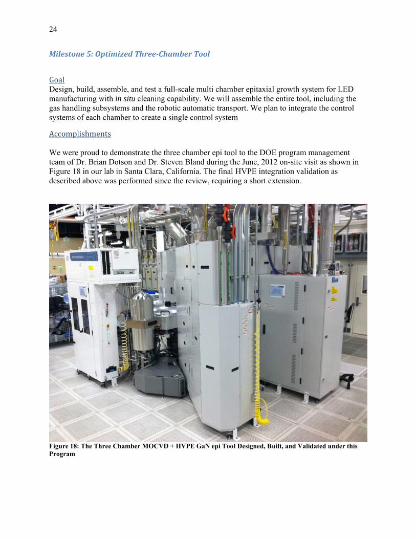
Accompl We wereteam of DFigure 18described
Figure 18:Program
ne5:Optim
build, assemturing with i
dling subsystof each cham
lishments
e proud to deDr. Brian Do8 in our lab id above was
: The Three C
mizedThree
mble, and testin situ cleaniems and the
mber to creat
emonstrate thotson and Drin Santa Claperformed s
Chamber MOC
e‐ChamberT
t a full-scale ing capabilitrobotic auto
te a single co
he three chamr. Steven Blaara, Californisince the rev
CVD + HVPE
Tool
multi chambty. We will aomatic transpontrol system
mber epi tooand during thia. The final view, requiri
GaN epi Too
ber epitaxialassemble theport. We plam
ol to the DOEhe June, 201HVPE integng a short ex
l Designed, Bu
l growth syse entire tool, an to integrat
E program m12 on-site visgration validxtension.
uilt, and Valid
stem for LEDincluding th
te the contro
management sit as showndation as
dated under th
D he ol
n in
his

25
CycleTi A key goLED GaNwas achiedepositio(MOCVD
The MQWgrown inshould beexchangethe cycle
Tab
Further cchamber MQW ancycle tim
Run #
1
2
3
4
5
6
7
8
9
10
etc.
imeReduc
oal of the proN process aneved. For a
on by HVPED) as shown
W process tin 1 hour. The noted that e time of 20 e time.
ble 9: Schema
cycle time opusing HVPE
nd p-GaN layme of 2.3 hrs.
# HVPE (2 h
0:00
2:00
4:00
6:00
8:00
10:00
12:00
14:00
16:00
18:00
…
tion
ogram was tond dedicating3 chamber c, a second ch
n in Figure 19
Figure 19
ime assumese cycle timethe u-GaN/nseconds for
atic for Cycle T
ptimization cE to deposit yers simultan. can be achi
TIM
hrs) MO MQ
2
5
8
11
14
0 17
0 20
0 23
0 2
0 5
o reduce the g chambers tconfigurationhamber for M9.
9: Sequential 3
s 5 pairs, wh per run can
n-GaN procthe robot to
Time with Ded
can be achiethe u-nGaN neously as sieved, far ex
ME START
QW (3 hrs) M
:00
:00
:00
1:00
4:00
7:00
0:00
3:00
:00
:00
…
cycle time oto specific pn, one chamMQW (MOC
3 chamber pr
hile the HVPn be reduced ess includesmove carrie
dicated u-GaN
ved by confifilm, and 2
shown in Figxceeding the
MO p‐GaN (1 hr
5:00
8:00
11:00
14:00
17:00
20:00
23:00
2:00
5:00
8:00
…
of epi manufprocesses, an
mber is dedicaCVD), and a
rocess (“1 + 1 +
E process timto 3.3 hrs. a a 1 hr. chamers through t
N/n-GaN , MQ
figuring the mchambers to
gure 20. Tabprogram go
Time out)
6:00
9:00
12:00
15:00
18:00
21:00
0:00
3:00
6:00
9:00
…
facturing. Byn improvemeated to u-Ga
a third chamb
+ 1”)
me assumedas shown in Tmber clean. the system h
QW and p-GaN
multi-chambo deposit viable 2 demonsal of 3.5 hou
Cycle(Elapsed Tim
4.5
4.0
3.7
3.6
3.5
3.4
3.3
3.3
3.3
…
y splitting thent in cycle taN/n-GaN ber for p-Ga
d 4 microns aTable 9. It Also, the
has no impac
N Chambers
ber tool witha MOCVD bstrates that aurs by 35%.
e time me / # Runs)
500
000
750
600
500
429
375
333
300
…
he time
aN
are
ct on
h one both a

26
Table
The workrespectivprocess f
R
e 10: Schemati
k we have dovely in the staflow and we
Run # HV
1
2
3
4
5
6
7
8
9
10
11
12
etc.
Figure 20:
ic for Cycle Ti
one previousandard sequare confirm
PE (2 hrs)
0:00
2:00
4:00
6:00
8:00
10:00
12:00
14:00
16:00
18:00
20:00
22:00
…
: Simultaneou
ime with DediC
sly to optimiential procesing the high
TIME START
MQW + p‐Ga(4 hrs)
2:00
6:00
10:00
14:00
18:00
22:00
…
us MQW/p-Ga
icated u-GaN/Chambers
ize chambersss flow is tra
h quality of r
T
N MQW (4
4
8
12
16
20
0
aN process (“1
/n-GaN Cham
s #2 and #3 ansferrable tresulting LE
Ti+ p‐GaN hrs)
:00
:00
2:00
6:00
0:00
:00
…
1 x 2”)
mber and Two
for MQW anto the new si
EDs
me out (E
6:00
8:00
10:00
12:00
14:00
16:00
18:00
20:00
22:00
0:00
2:00
4:00
…
o MQW-p-GaN
nd p-GaN imultaneous
Cycle time lapsed Time / #
Runs)
4.000
3.333
3.000
2.800
2.667
2.571
2.500
2.444
2.400
2.364
2.333
…
N
#

27
ProjectActivitySummary
Originalhypotheses The original Statement of Program Objectives (SOPO) is listed below.
OBJECTIVESTHE RECIPIENT proposes to develop a multi-chamber system such as a two MOCVD chambers, one HVPE chamber, lamp heating, and automated in situ cleaning. The system shall be capable of growing high-quality LEDs on substrate materials currently in commercial use or under consideration. It shall contain a 300-mm or larger platter that holds 28 two-inch wafers. THE RECIPIENT shall build it on the successful Centura (TM) platform, the standard for growing low-cost, high-quality epitaxial wafers in the integrated circuit industry. The proposed system shall decrease operating costs through a combination of decreasing cycle time, increasing throughput, using in-situ cleaning, and decreasing the cost of chemicals. It shall increase the internal quantum efficiency of LEDs by reducing the density of extended defects and point defects. It shall improve binning yields by improving the uniformity of wavelength and output power within the wafer, from wafer to wafer, and from run to run. TASKSTOBEPERFORMED
ProjectManagement andPlanningTHE RECIPIENT shall develop and maintain a Project Management Plan (PMP) throughout the course of the project. The initial PMP shall be submitted to the DOE Project Officer within 60 days of award. The Recipient shall review and update the PMP at the end of each Budget Period and resubmit as a part of the budget period continuation application. The PMP shall also be modified on an ad hoc basis to reflect significant changes or deviations of planning. Multi‐WaferHVPEEpiChamberTHE RECIPIENT shall design and assemble a multi-wafer nitride HVPE system for high volume production. The goal shall be to identify a chamber design and compatible process conditions that can deposit high-quality GaN at a growth rate of several microns per hour. THE RECIPIENT shall test multiple approaches to injecting reagents into the reactor chamber to optimize mixing and uniform distribution of reagent gases. THE RECIPIENT shall optimize growth parameters such as temperature, pressure, V:III ratio, carrier flow rate, and total gas flow. u-GaN and MQW layer thickness uniformities shall be monitored both within wafer (w-i-w) and wafer to wafer (w-2-w) across a multi-wafer carrier. The recipient shall have the goal of controlling GaN layer thickness uniformity with a standard deviation below 2%. THE RECIPIENT shall optimize the chamber design for the requisite temperature control. The HVPE system shall have a goal of achieving contaminant levels below 1016 atoms/cm3 for chlorine and oxygen. The HVPE

28
system shall be suitable for a cluster deposition system that also incorporates MOCVD chambers. At the end of Task 2, THE RECIPIENT shall test the system for the following criteria:
Growth of 4-micron GaN layer Temperature uniformity across the carrier GaN thickness uniformity within the wafer GaN thickness uniformity wafer-to-wafer GaN crystalline quality (threading dislocations per cm2) Contaminant levels for Oxygen and Chlorine
EpiToolwithmultiChamberSplitProcessTHE RECIPIENT shall design and build a multi-chamber, split-process Epi tool that with the goal of increasing throughput and minimizing PL wavelength drift. The system shall have the ability to grow HT-GaN template in one chamber and MQW layers in another chamber. THE RECIPIENT shall have a target both w-i-w and w-2-w PL wavelength uniformity of 2 nm or better. THE RECIPIENT shall integrate precise multi-zone temperature controls and process gas flow controls into the production ready Epi tool. THE RECIPIENT shall develop a process recipe with the goal of optimizing the multi-chamber system such as a MOCVD / HVPE (2+1) system described above to be capable of fabricating LEDs with internal quantum efficiency up to 75%. THE RECIPIENT shall test the multi-chamber MOCVD / HVPE system for the following properties:
EL Uniformity Within the Wafer PL Uniformity Within the Wafer PL Uniformity Wafer-to-Wafer PL Uniformity Run-to-Run Run-to-Run Std. Dev. IQE
ProcessforGrowingLow‐Defect,High‐QualityLEDStructuresontheMostIndustriallyRelevantSubstratesTHE RECIPIENT shall have the goal of demonstrating that the multi-chamber, split-process Epi prototype developed in Task 3 can deposit high-quality GaN material (including ternary and quaternary alloys) on at least two substrates. The process development shall focus on optimizing crystal quality and uniformity, and exploring process parameters with a goal of elucidating GaN, GaInN, and AlInGaN epitaxial growth mechanisms.
In‐SituCleaningProcessTHE RECIPIENT shall develop an in situ cleaning process for the MOCVD chamber using halogen-based etching gases, with the goal of delivering a clean showerhead, with minimal residual GaCl3, that does not adversely affect the crystal quality of the GaN layers in a subsequent run. THE RECIPIENT shall demonstrate in situ cleaning time with a goal of reaching 1 hour clean time. THE RECIPIENT shall have a goal that the in situ cleaning makes it possible to complete at least 5 MOCVD chamber runs without breaking vacuum and without

29
affecting the crystal quality of LED structures created in the next run or in succeeding runs.
Optimizedmulti‐ChamberEpiToolTHE RECIPIENT shall assemble an optimized multi-chamber system such as a MOCVD / HVPE (2+1) system capable of growing high quality HB-LEDs with low defect densities on multi-wafer carriers. THE RECIPIENT shall equip the MOCVD process chambers with in situ cleaning capability for enhanced throughput, high binning yield, and minimal deviations in PL/EL/thickness uniformity.
Approachesused Key aspects to our technical approach are itemized below.
1. Validate our baseline approach for low-cost split process GaN growth: focus on each layer and then on integration
a. u-GaN/n-GaN (Si-doped) b. MQW c. p-GaN (Mg-doped)
2. Create a multi-chamber MOCVD / HVPE system (2 MOCVD +1 HVPE). 3. Create a novel subsystem for automated in situ cleaning of the deposition chambers. 4. Control the growth temperature with precision high-speed lamp heating. 5. Reduce material defects by taking advantage of the flexible configuration of Applied
Material’s CenturaTM deposition chambers.
The multi-chamber architecture enabled an innovative approach to growing the hetero-epitaxial layer by using dedicated chambers for each of the major segments in the epi stack: u-GaN/n-GaN, MQW, and p-GaN.

30
Problemsencountered HVPE uniformity from wafer to wafer was a challenge that we overcame, but took longer than expected to validate. The challenges and progress in our HVPE development was reported monthly to our program manager. The main unforeseen issue for this program, however, was the market condition for LED GaN epi tools after early 2011. The so-called “crash” in tool sales for the LED industry was unexpected in its severity and suddenness. Additionally, since Applied was new to the market, customers demanded that we demonstrate world class LEDs and process controls before purchasing agreements could be completed. This caused understandable delays and although we were able to demonstrate world-class results as described above, the market collapse limited the sales in 2012. The future of the tool developed, however, is especially bright for GaN on silicon manufacturing given the ability to separate processes as well as cost-effective large diameter (>12”) thick GaN templates with GaN thickness greater than 20um.

31
Productsdevelopedundertheaward
Networksorcollaborationsfostered Strong partnerships were fostered with academia, national labs, and other companies through this program. We found the DOESSL Workshops very helpful in making contacts and fostering discussions. One particularly strong collaboration was with Sandia National Labs for third party validation of our GaN process and metrology we were not able to perform, which was particularly helpful to Applied Materials.
Technologies/Techniques A number of key technologies as shown by the inventions below were developed during the course of this program which helped Applied Materials develop key technologies for the GaN epi market. In addition, jobs were created and saved in Santa Clara, California
Inventions/PatentApplications Five patent applications were submitted through this program thanks to the support of the DOE:

32
Summary Over the course of this program, Applied Materials, Inc., with generous support from the United States Department of Energy, developed a world-class three chamber III-Nitride epi cluster tool for low-cost, high volume GaN growth for the solid state lighting industry. One of the major achievements of the program was to design, build, and demonstrate the world’s largest wafer capacity HVPE chamber suitable for repeatable high volume III-Nitride template and device manufacturing. Applied Materials’ experience in developing deposition chambers for the silicon chip industry over many decades resulted in many orders of magnitude reductions in the price of transistors. That experience and understanding was used in developing this GaN epi deposition tool. The multi-chamber approach, which continues to be unique in the ability of the each chamber to deposit a section of the full device structure, unlike other cluster tools, allows for extreme flexibility in the manufacturing process. This robust architecture is suitable for not just the LED industry, but GaN power devices as well, both horizontal and vertical designs. The new HVPE technology developed allows GaN to be grown at a rate unheard of with MOCVD, up to 20x the typical MOCVD rates of 3m per hour, with bulk crystal quality as better than the highest-quality commercial GaN films grown by MOCVD at a much cheaper overall cost. This is a unique development as the HVPE process has been known for decades, but never successfully commercially developed for high volume manufacturing. This research shows the potential of the first commercial-grade HVPE chamber, an elusive goal for III-V researchers and those wanting to capitalize on the promise of HVPE. Additionally, in the course of this program, Applied Materials built two MOCVD chambers, in addition to the HVPE chamber, and a robot that moves wafers between them. The MOCVD chambers demonstrated industry-leading wavelength yield for GaN based LED wafers and industry-leading uptime enabled in part by a novel in-situ cleaning process developed in this program. The Department of Energy was a great supporter of this leading-edge technology that can benefit U.S. industry and keep GaN manufacturing competitive in the United States. We gratefully acknowledge their role in advancing the state-of-the-art.

33
Acknowledgements "This material is based upon work supported by the Department of Energy under Award Number DE-EE0003331." We gratefully acknowledge the hard work of the DOE in developing and managing this important program. We particularly are grateful to or program manager, Brian Dotson of NETL, who has guided us and provided very helpful advice.
Also, we wish to thank Jim Brodrick, the solid-state lighting (SSL) portfolio manager in the DOE's Office of Energy Efficiency and Renewable Energy. His vision for solid state lighting and manufacturing helped to successfully execute programs like ours which are key in providing the investment in driving technology forward.
Finally, we wish to thank Sean Evans, our initial program manager at NETL.