Embed Size (px)
Citation preview
Integrated Silicon Solution, Inc. - www.issi.com 1Rev. C12/01/09
Copyright © 2006 Integrated Silicon Solution, Inc. All rights reserved. ISSI reserves the right to make changes to this specification and its products at any time with-out notice. ISSI assumes no liability arising out of the application or use of any information, products or services described herein. Customers are advised to obtain the latest version of this device specification before relying on any published information and before placing orders for products.
IS42S32800DIS45S32800D
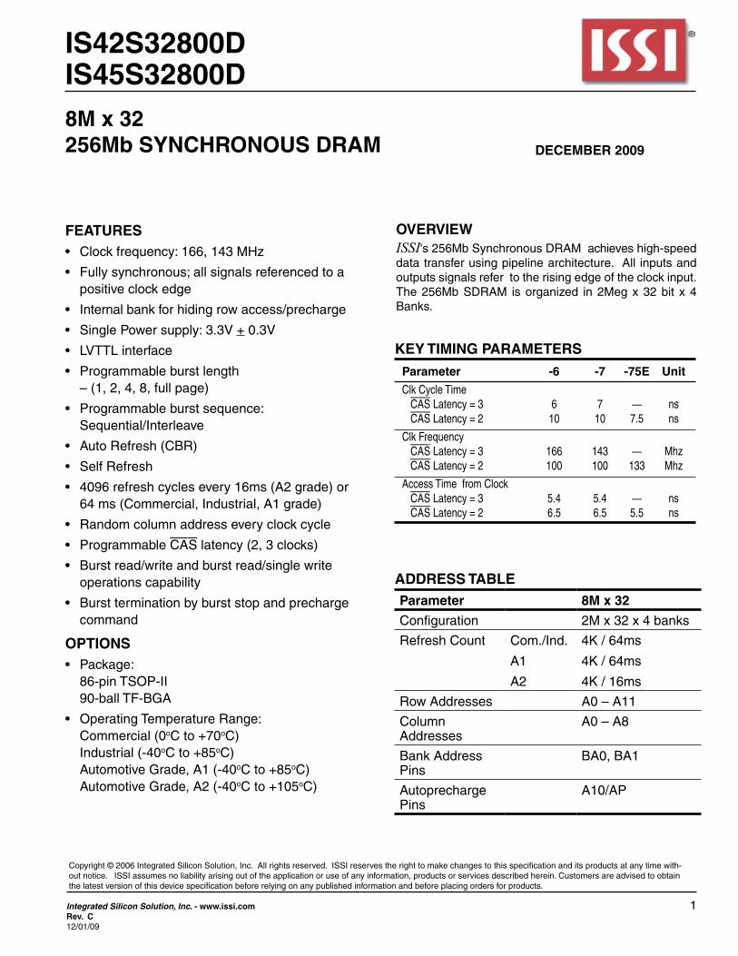
FEATURES• Clockfrequency:166,143MHz
• Fullysynchronous;allsignalsreferencedtoapositive clock edge
• Internalbankforhidingrowaccess/precharge
• SinglePowersupply:3.3V+0.3V
• LVTTLinterface
• Programmableburstlength –(1,2,4,8,fullpage)
• Programmableburstsequence: Sequential/Interleave
• AutoRefresh(CBR)
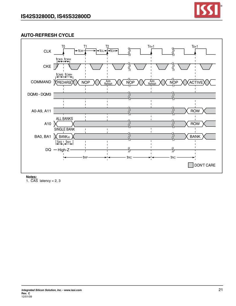
• SelfRefresh
• 4096refreshcyclesevery16ms(A2grade)or64ms(Commercial,Industrial,A1grade)
• Randomcolumnaddresseveryclockcycle
• ProgrammableCASlatency(2,3clocks)
• Burstread/writeandburstread/singlewrite operations capability
• Burstterminationbyburststopandprechargecommand
OPTIONS• Package:
86-pinTSOP-II 90-ballTF-BGA
• OperatingTemperatureRange: Commercial (0oC to +70oC) Industrial(-40oCto+85oC) AutomotiveGrade,A1(-40oCto+85oC) AutomotiveGrade,A2(-40oCto+105oC)
OVERVIEWISSI's256MbSynchronousDRAMachieveshigh-speeddata transfer using pipeline architecture. All inputs and outputs signals refer to the rising edge of the clock input.The256MbSDRAM isorganized in2Megx32bit x4Banks.
8M x 32 256Mb SYNCHRONOUS DRAM DECEMBER 2009
KEY TIMING PARAMETERS
Parameter -6 -7 -75E Unit
ClkCycleTime CASLatency=3 6 7 — ns CASLatency=2 10 10 7.5 ns
ClkFrequency CASLatency=3 166 143 — Mhz CASLatency=2 100 100 133 Mhz
AccessTimefromClock CASLatency=3 5.4 5.4 — ns CASLatency=2 6.5 6.5 5.5 ns
ADDRESS TABLEParameter 8M x 32
Configuration 2Mx32x4banks
RefreshCount Com./Ind.
A1
A2
4K/64ms
4K/64ms
4K/16ms
RowAddresses A0 – A11
Column Addresses
A0–A8
BankAddressPins
BA0,BA1
Autoprecharge Pins
A10/AP
2 Integrated Silicon Solution, Inc. - www.issi.comRev. C
12/01/09
IS42S32800D, IS45S32800D
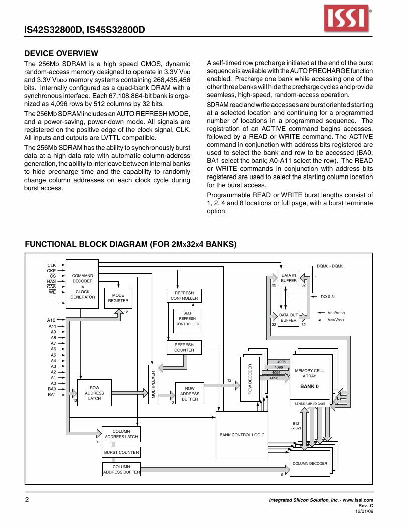
DEVICE OVERVIEWThe 256Mb SDRAM is a high speed CMOS, dynamicrandom-accessmemorydesignedtooperatein3.3VVdd and3.3VVddq memorysystemscontaining268,435,456bits.Internallyconfiguredasaquad-bankDRAMwithasynchronousinterface.Each67,108,864-bitbankisorga-nizedas4,096rowsby512columnsby32bits.
The256MbSDRAMincludesanAUTOREFRESHMODE,and a power-saving, power-down mode. All signals are registeredonthepositiveedgeoftheclocksignal,CLK.AllinputsandoutputsareLVTTLcompatible.
The256MbSDRAMhastheabilitytosynchronouslyburstdata at a high data rate with automatic column-address generation, the ability to interleave between internal banks to hide precharge time and the capability to randomly change column addresses on each clock cycle during burst access.
A self-timed row precharge initiated at the end of the burst sequenceisavailablewiththeAUTOPRECHARGEfunctionenabled. Precharge one bank while accessing one of the other three banks will hide the precharge cycles and provide seamless, high-speed, random-access operation.
SDRAM read and write accesses are burst oriented starting at a selected location and continuing for a programmed number of locations in a programmed sequence. Theregistration of an ACTIVE command begins accesses,followedbyaREADorWRITEcommand.TheACTIVEcommand in conjunction with address bits registered are usedtoselect thebankandrowtobeaccessed(BA0,BA1selectthebank;A0-A11selecttherow).TheREADor WRITE commands in conjunction with address bitsregistered are used to select the starting column location for the burst access.
ProgrammableREADorWRITEburstlengthsconsistof1,2,4and8locationsorfullpage,withaburstterminateoption.
CLKCKE
CSRASCASWE
A9A8A7A6A5A4A3A2A1A0
BA0BA1
A10
COMMANDDECODER
&CLOCK
GENERATOR MODEREGISTER
REFRESHCONTROLLER
REFRESHCOUNTER
SELF
REFRESH
CONTROLLER
ROWADDRESS
LATCH MU
LTIP
LEX
ER
COLUMNADDRESSLATCH
BURSTCOUNTER
COLUMNADDRESSBUFFER
COLUMNDECODER
DATAINBUFFER
DATAOUTBUFFER
DQM0-DQM3
DQ0-31
VDD/VDDQ
Vss/VssQ
12
12
9
12
12
9
32
32 32
32
512(x32)
4096
4096
4096
RO
WD
EC
OD
ER 4096
MEMORYCELLARRAY
BANK 0
SENSEAMPI/OGATE
BANKCONTROLLOGIC
ROWADDRESSBUFFER
A11
4
FUNCTIONAL BLOCK DIAGRAM (FOR 2Mx32x4 BANKS)
IS42S32800D, IS45S32800D
Integrated Silicon Solution, Inc. - www.issi.com 3Rev. C12/01/09
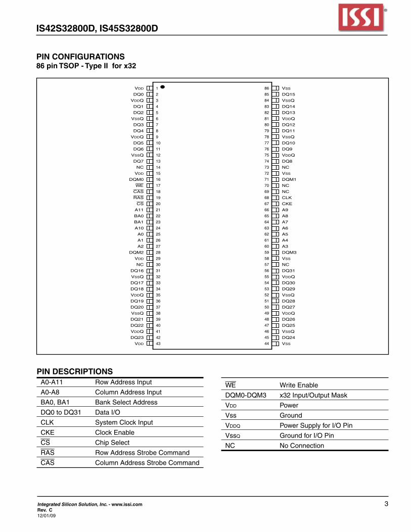
PIN CONFIGURATIONS86 pin TSOP - Type II for x32
PIN DESCRIPTIONSA0-A11 RowAddressInput
A0-A8 ColumnAddressInput
BA0,BA1 BankSelectAddress
DQ0toDQ31 DataI/O
CLK SystemClockInput
CKE ClockEnable
CS Chip Select
RAS RowAddressStrobeCommand
CAS Column Address Strobe Command
VDD
DQ0
VDDQ
DQ1
DQ2
VSSQ
DQ3
DQ4
VDDQ
DQ5
DQ6
VSSQ
DQ7
NC
VDD
DQM0
WE
CAS
RAS
CS
A11
BA0
BA1
A10
A0
A1
A2
DQM2
VDD
NC
DQ16
VSSQ
DQ17
DQ18
VDDQ
DQ19
DQ20
VSSQ
DQ21
DQ22
VDDQ
DQ23
VDD
1
2
3
4
5
6
7
8
9
10
11
12
13
14
15
16
17
18
19
20
21
22
23
24
25
26
27
28
29
30
31
32
33
34
35
36
37
38
39
40
41
42
43
86
85
84
83
82
81
80
79
78
77
76
75
74
73
72
71
70
69
68
67
66
65
64
63
62
61
60
59
58
57
56
55
54
53
52
51
50
49
48
47
46
45
44
VSS
DQ15
VSSQ
DQ14
DQ13
VDDQ
DQ12
DQ11
VSSQ
DQ10
DQ9
VDDQ
DQ8
NC
VSS
DQM1
NC
NC
CLK
CKE
A9
A8
A7
A6
A5
A4
A3
DQM3
VSS
NC
DQ31
VDDQ
DQ30
DQ29
VSSQ
DQ28
DQ27
VDDQ
DQ26
DQ25
VSSQ
DQ24
VSS
WE WriteEnable
DQM0-DQM3 x32Input/OutputMask
Vdd Power
Vss Ground
Vddq PowerSupplyforI/OPin
Vssq GroundforI/OPin
NC NoConnection
4 Integrated Silicon Solution, Inc. - www.issi.comRev. C
12/01/09
IS42S32800D, IS45S32800D
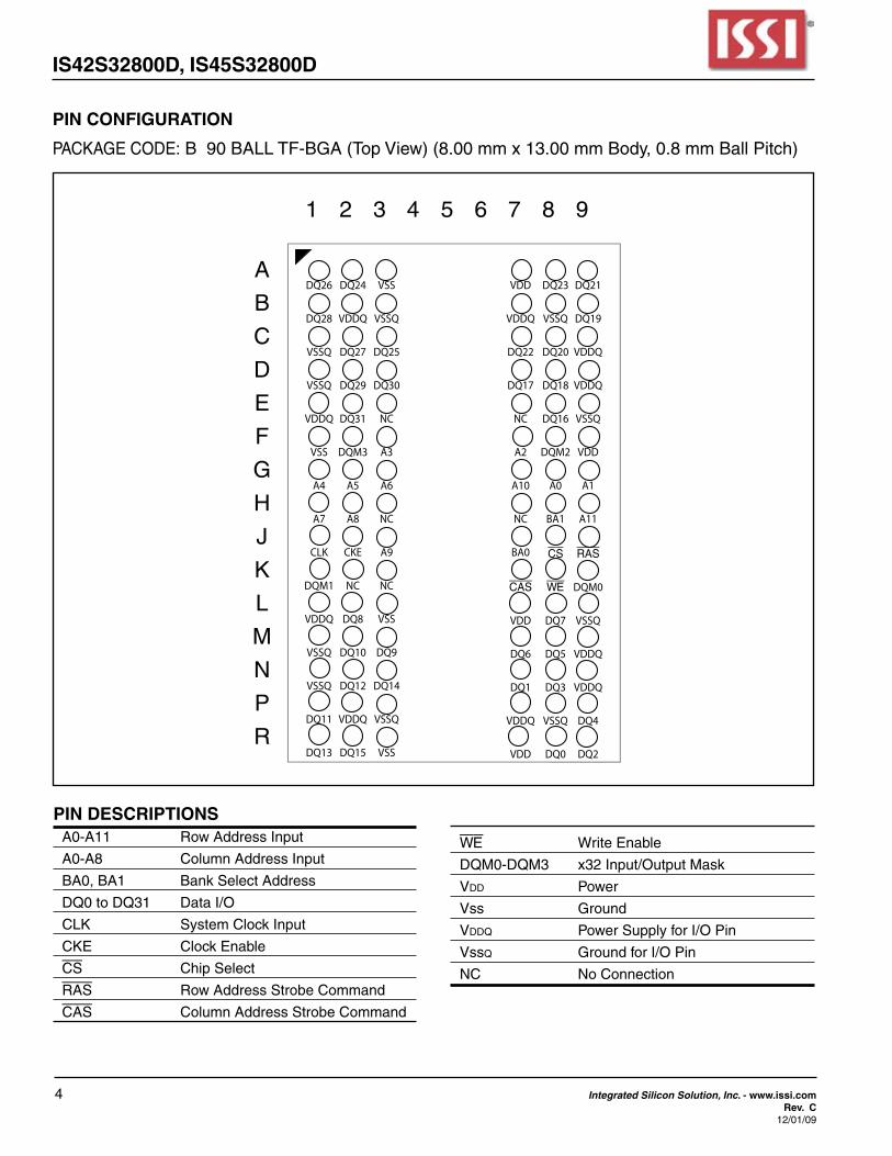
PIN CONFIGURATION
PACKAGECODE:B90BALLTF-BGA(TopView)(8.00mmx13.00mmBody,0.8mmBallPitch)
1 2 3 4 5 6 7 8 9
A
B
C
D
E
F
G
H
J
K
L
M
N
P
R
DQ26
DQ28
VSSQ
VSSQ
VDDQ
VSS
A4
A7
CLK
DQM1
VDDQ
VSSQ
VSSQ
DQ11
DQ13
DQ24
VDDQ
DQ27
DQ29
DQ31
DQM3
A5
A8
CKE
NC
DQ8
DQ10
DQ12
VDDQ
DQ15
VSS
VSSQ
DQ25
DQ30
NC
A3
A6
NC
A9
NC
VSS
DQ9
DQ14
VSSQ
VSS
VDD
VDDQ
DQ22
DQ17
NC
A2
A10
NC
BA0
CAS
VDD
DQ6
DQ1
VDDQ
VDD
DQ23
VSSQ
DQ20
DQ18
DQ16
DQM2
A0
BA1
CS
WE
DQ7
DQ5
DQ3
VSSQ
DQ0
DQ21
DQ19
VDDQ
VDDQ
VSSQ
VDD
A1
A11
RAS
DQM0
VSSQ
VDDQ
VDDQ
DQ4
DQ2
PIN DESCRIPTIONSA0-A11 RowAddressInput
A0-A8 ColumnAddressInput
BA0,BA1 BankSelectAddress
DQ0toDQ31 DataI/O
CLK SystemClockInput
CKE ClockEnable
CS Chip Select
RAS RowAddressStrobeCommand
CAS Column Address Strobe Command
WE WriteEnable
DQM0-DQM3 x32Input/OutputMask
Vdd Power
Vss Ground
Vddq PowerSupplyforI/OPin
Vssq GroundforI/OPin
NC NoConnection
IS42S32800D, IS45S32800D
Integrated Silicon Solution, Inc. - www.issi.com 5Rev. C12/01/09
PIN FUNCTIONS Symbol Type Function (In Detail)
A0-A11 InputPin AddressInputs:A0-A11aresampledduringtheACTIVE
command(row-addressA0-A11)andREAD/WRITEcommand(columnaddressA0-A8),withA10definingautoprecharge)toselectonelocationoutofthememoryarrayintherespectivebank.A10issampledduringaPRECHARGEcommandtodetermineifallbanksaretobeprecharged(A10HIGH)orbankselectedby BA0,BA1(LOW).Theaddressinputsalsoprovidetheop-codeduringaLOADMODEREGISTERcommand.
BA0,BA1 InputPin BankSelectAddress:BA0andBA1defineswhichbanktheACTIVE,READ,WRITEorPRECHARGEcommandisbeingapplied.
CAS InputPin CAS, in conjunction with the RAS and WE, forms the device command. See the "CommandTruthTable"fordetailsondevicecommands.
CKE InputPin TheCKEinputdetermineswhethertheCLKinputisenabled.ThenextrisingedgeoftheCLKsignalwillbevalidwhenisCKEHIGHandinvalidwhenLOW.WhenCKEisLOW,thedevicewillbeineitherpower-downmode,clocksuspendmode,orselfrefresh mode. CKEisan asynchronous input.
CLK InputPin CLKisthemasterclockinputforthisdevice.ExceptforCKE,allinputstothisdeviceareacquiredinsynchronizationwiththerisingedgeofthispin.
CS InputPin TheCS input determines whether command input is enabled within the device. Command input is enabled when CSisLOW,anddisabledwithCSisHIGH.Thedevice remains in the previous state when CSisHIGH.
DQM0-DQM3 InputPin DQM0-DQM3controlthefourbytesoftheI/Obuffers(DQ0-DQ31).Inread
mode,DQMncontroltheoutputbuffer.WhenDQMnisLOW,thecorrespondingbuf-ferbyteisenabled,andwhenHIGH,disabled.TheoutputsgototheHIGHimped-ancestatewhenDQMnisHIGH.ThisfunctioncorrespondstoOE in conventional DRAMs.Inwritemode,DQMncontroltheinputbuffer.WhenDQMnisLOW,thecorrespondingbufferbyteisenabled,anddatacanbewrittentothedevice.WhenDQMnisHIGH,inputdataismaskedandcannotbewrittentothedevice.
DQ0-DQ31 Input/OutputPin DataontheDataBusislatchedonthesepinsduringWritecommands,andbufferedafterReadcommands.
RAS InputPin RAS, in conjunction with CAS and WE, forms the device command. See the "Com-mandTruthTable"itemfordetailsondevicecommands.
WE InputPin WE, in conjunction with RAS and CAS, forms the device command. See the "Com-mandTruthTable"itemfordetailsondevicecommands.
Vddq PowerSupplyPin Vddq is the output buffer power supply.
Vdd PowerSupplyPin Vdd is the device internal power supply.
Vssq PowerSupplyPin Vssq is the output buffer ground.
Vss PowerSupplyPin Vss is the device internal ground.
6 Integrated Silicon Solution, Inc. - www.issi.comRev. C
12/01/09
IS42S32800D, IS45S32800D
GENERAL DESCRIPTION
READTheREADcommandselectsthebankfromBA0,BA1inputsand starts a burst read access to an active row. Inputs A0-A8providesthestartingcolumnlocation.WhenA10isHIGH,thiscommandfunctionsasanAUTOPRECHARGEcommand.Whentheautoprechargeisselected,therowbeingaccessedwillbeprechargedattheendoftheREADburst.TherowwillremainopenforsubsequentaccesseswhenAUTOPRECHARGE isnot selected. DQ’s readdataissubjecttothelogiclevelontheDQMinputstwoclocksearlier.WhenagivenDQMsignalwasregisteredHIGH,thecorrespondingDQ’swillbeHigh-Ztwoclockslater.DQ’swillprovidevaliddatawhentheDQMsignalwasregisteredLOW.
WRITEA burst write access to an active row is initiated with the WRITE command. BA0, BA1 inputs selects the bank,and the starting column location is provided by inputs A0-A8.Whether or notAUTO-PRECHARGE is used isdetermined by A10.
TherowbeingaccessedwillbeprechargedattheendoftheWRITEburst, ifAUTOPRECHARGE isselected. IfAUTOPRECHARGEisnotselected,therowwillremainopenforsubsequentaccesses.
A memory array is written with corresponding input data onDQ’sandDQMinputlogiclevelappearingatthesametime.DatawillbewrittentomemorywhenDQMsignalisLOW.WhenDQMisHIGH,thecorrespondingdatainputswillbeignored,andaWRITEwillnotbeexecutedtothatbyte/column location.
PRECHARGEThePRECHARGEcommand isused todeactivate theopen row in a particular bank or the open row in all banks. BA0,BA1canbeusedtoselectwhichbankisprechargedor they are treated as “Don’t Care”. A10 determinedwhetheroneorallbanksareprecharged.Afterexecut-ing this command, the next command for the selectedbank(s)isexecutedafterpassageoftheperiodtRP, which istheperiodrequiredforbankprecharging.Onceabankhas been precharged, it is in the idle state and must be activatedpriortoanyREADorWRITEcommandsbeingissued to that bank.
AUTO PRECHARGETheAUTOPRECHARGEfunctionensuresthatthepre-charge is initiated at the earliest valid stage within a burst. Thisfunctionallowsforindividual-bankprechargewithoutrequiringanexplicitcommand.A10toenabletheAUTO
PRECHARGEfunctioninconjunctionwithaspecificREADorWRITEcommand.ForeachindividualREADorWRITEcommand, auto precharge is either enabled or disabled. AUTOPRECHARGEdoesnotapplyexceptinfull-pageburst mode. Upon completion of the READ or WRITEburst, a precharge of the bank/row that is addressed is automatically performed.
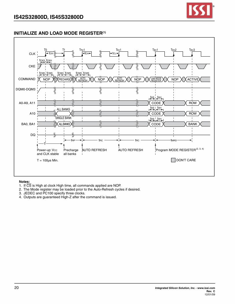
AUTO REFRESH COMMANDThiscommandexecutestheAUTOREFRESHoperation.Therowaddressandbanktoberefreshedareautomaticallygeneratedduringthisoperation. Thestipulatedperiod(trc)isrequiredforasinglerefreshoperation,andnoothercom-mandscanbeexecutedduringthisperiod. Thiscommandisexecutedatleast4096timesforeveryTref.DuringanAUTOREFRESHcommand,addressbitsare“Don’tCare”.ThiscommandcorrespondstoCBRAuto-refresh.
BURST TERMINATETheBURSTTERMINATEcommand forcibly terminatesthe burst read and write operations by truncating either fixed-length or full-page bursts and the most recentlyregisteredREADorWRITEcommandpriortotheBURSTTERMINATE.
COMMAND INHIBITCOMMANDINHIBITpreventsnewcommandsfrombeingexecuted.Operationsinprogressarenotaffected,apartfromwhethertheCLKsignalisenabled
NO OPERATION WhenCSislow,theNOPcommandpreventsunwantedcommands from being registered during idle or wait states.
LOAD MODE REGISTERDuringtheLOADMODEREGISTERcommandthemoderegisterisloadedfromA0-A11.Thiscommandcanonlybe issued when all banks are idle.
ACTIVE COMMANDWhen the ACTIVE COMMAND is activated, BA0, BA1inputs selects a bank to be accessed, and the address inputsonA0-A11selectstherow.UntilaPRECHARGEcommand is issued to the bank, the row remains open for accesses.
IS42S32800D, IS45S32800D
Integrated Silicon Solution, Inc. - www.issi.com 7Rev. C12/01/09
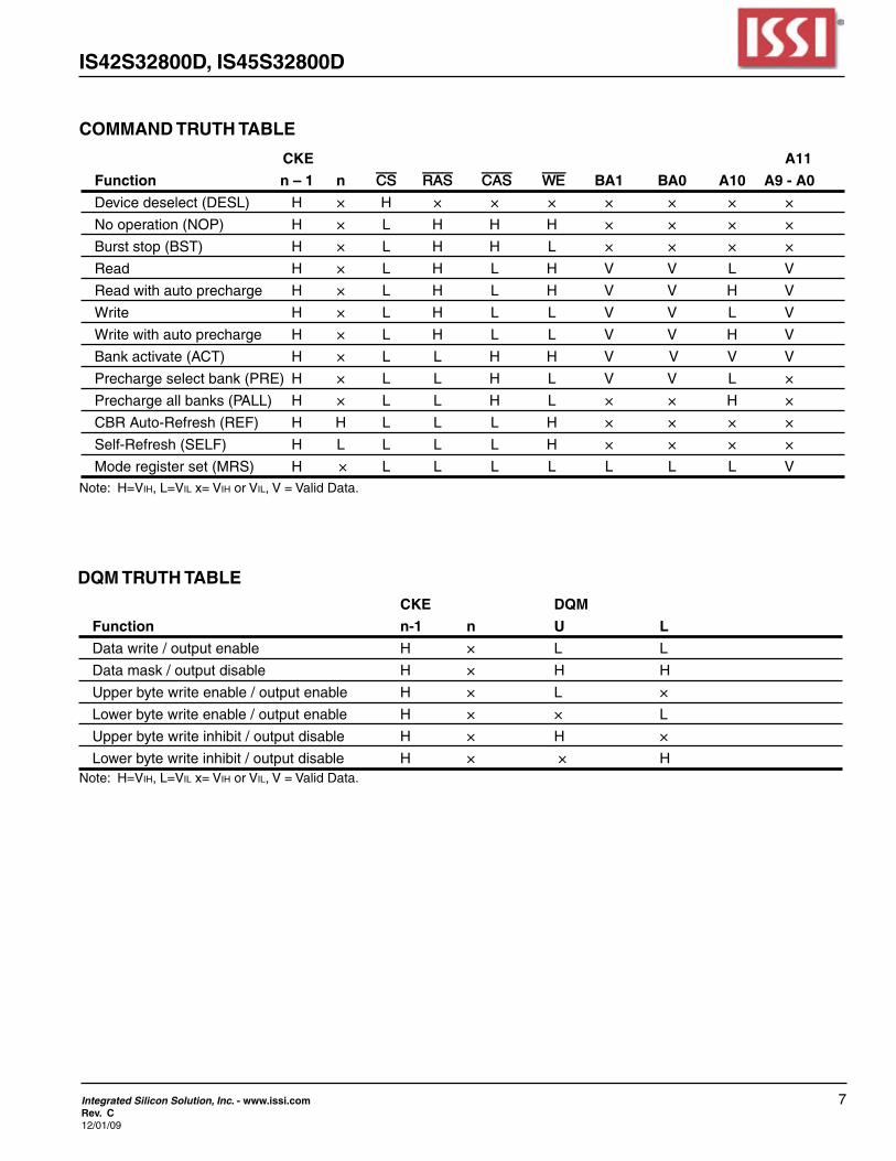
CKE DQM
Function n-1 n U L
Datawrite/outputenable H × L L
Datamask/outputdisable H × H H
Upperbytewriteenable/outputenable H × L ×
Lowerbytewriteenable/outputenable H × × L
Upperbytewriteinhibit/outputdisable H × H ×
Lowerbytewriteinhibit/outputdisable H × × H
CKE A11
Function n – 1 n CS RAS CAS WE BA1 BA0 A10 A9 - A0
Devicedeselect(DESL) H × H × × × × × × ×
Nooperation(NOP) H × L H H H × × × ×
Burststop(BST) H × L H H L × × × ×
Read H × L H L H V V L V
Readwithautoprecharge H × L H L H V V H V
Write H × L H L L V V L V
Writewithautoprecharge H × L H L L V V H V
Bankactivate(ACT) H × L L H H V V V V
Prechargeselectbank(PRE) H × L L H L V V L ×
Prechargeallbanks(PALL) H × L L H L × × H ×
CBRAuto-Refresh(REF) H H L L L H × × × ×
Self-Refresh(SELF) H L L L L H × × × ×
Moderegisterset(MRS) H × L L L L L L L V
COMMAND TRUTH TABLE
DQM TRUTH TABLE
Note:H=Vih,L=Vilx=VihorVil,V=ValidData.
Note:H=Vih,L=Vilx=VihorVil,V=ValidData.
8 Integrated Silicon Solution, Inc. - www.issi.comRev. C
12/01/09
IS42S32800D, IS45S32800D
CKE
CurrentState/Function n–1 n CS RAS CAS WE Address
ActivatingClocksuspendmodeentry H L × × × × ×
AnyClocksuspendmode L L × × × × ×
Clocksuspendmodeexit L H × × × × ×
AutorefreshcommandIdle(REF) H H L L L H ×
SelfrefreshentryIdle(SELF) H L L L L H ×
PowerdownentryIdle H L × × × × ×
Selfrefreshexit L H L H H H × L H H × × × ×
Powerdownexit L H × × × × ×
Note:H=Vih,L=Vilx=VihorVil,V=ValidData.
CKE TRUTH TABLE
IS42S32800D, IS45S32800D
Integrated Silicon Solution, Inc. - www.issi.com 9Rev. C12/01/09
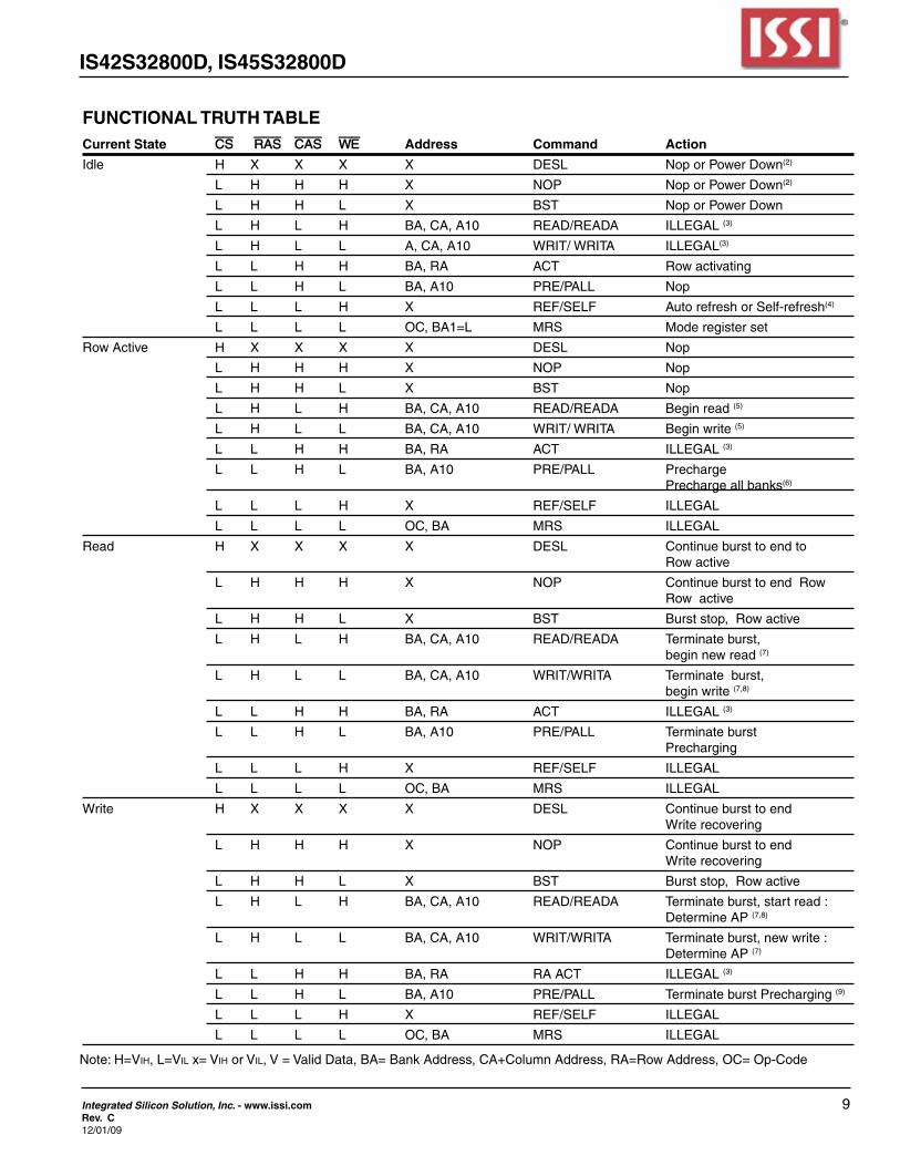
Current State CS RAS CAS WE Address Command Action
Idle H X X X X DESL NoporPowerDown(2)
L H H H X NOP NoporPowerDown(2)
L H H L X BST NoporPowerDown
L H L H BA,CA,A10 READ/READA ILLEGAL(3)
L H L L A,CA,A10 WRIT/WRITA ILLEGAL(3)
L L H H BA,RA ACT Rowactivating
L L H L BA,A10 PRE/PALL Nop
L L L H X REF/SELF AutorefreshorSelf-refresh(4)
L L L L OC,BA1=L MRS Moderegisterset
RowActive H X X X X DESL Nop
L H H H X NOP Nop
L H H L X BST Nop
L H L H BA,CA,A10 READ/READA Beginread(5)
L H L L BA,CA,A10 WRIT/WRITA Beginwrite(5)
L L H H BA,RA ACT ILLEGAL(3)
L L H L BA,A10 PRE/PALL Precharge
Prechargeallbanks(6)
L L L H X REF/SELF ILLEGAL
L L L L OC,BA MRS ILLEGAL
Read H X X X X DESL Continuebursttoendto Rowactive
L H H H X NOP ContinuebursttoendRow Rowactive
L H H L X BST Burststop,Rowactive
L H L H BA,CA,A10 READ/READA Terminateburst, begin new read (7)
L H L L BA,CA,A10 WRIT/WRITA Terminateburst, begin write (7,8)
L L H H BA,RA ACT ILLEGAL(3)
L L H L BA,A10 PRE/PALL Terminateburst Precharging
L L L H X REF/SELF ILLEGAL
L L L L OC,BA MRS ILLEGAL
Write H X X X X DESL Continuebursttoend Writerecovering
L H H H X NOP Continuebursttoend Writerecovering
L H H L X BST Burststop,Rowactive
L H L H BA,CA,A10 READ/READA Terminateburst,startread: DetermineAP(7,8)
L H L L BA,CA,A10 WRIT/WRITA Terminateburst,newwrite: DetermineAP(7)
L L H H BA,RA RAACT ILLEGAL(3)
L L H L BA,A10 PRE/PALL TerminateburstPrecharging(9)
L L L H X REF/SELF ILLEGAL
L L L L OC,BA MRS ILLEGAL
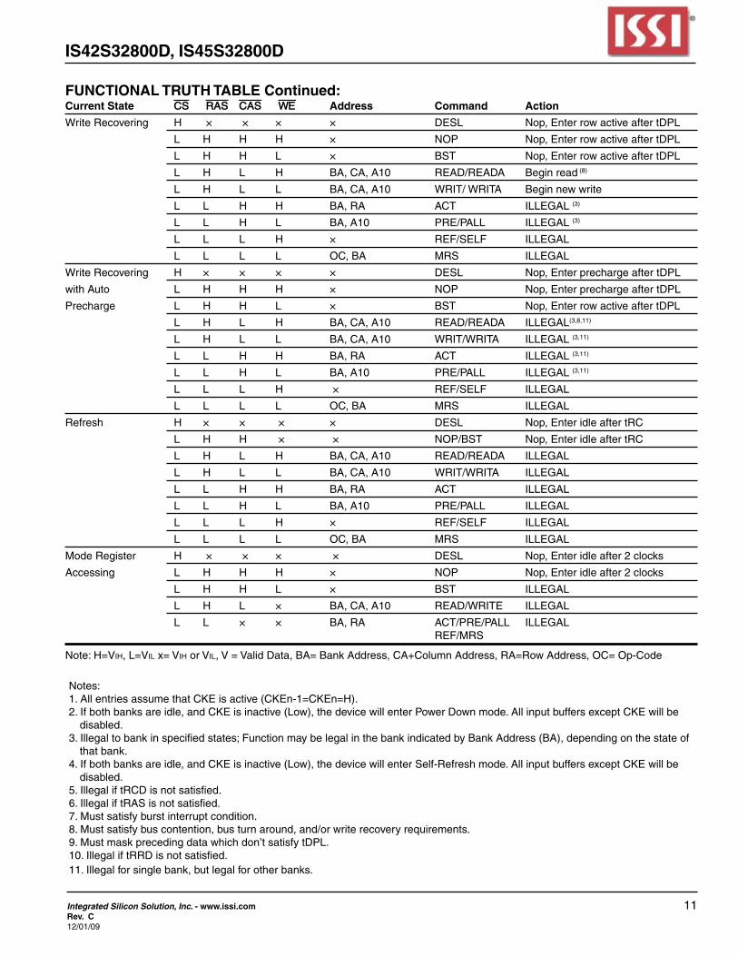
FUNCTIONAL TRUTH TABLE
Note:H=Vih,L=Vilx=VihorVil,V=ValidData,BA=BankAddress,CA+ColumnAddress,RA=RowAddress,OC=Op-Code
10 Integrated Silicon Solution, Inc. - www.issi.comRev. C
12/01/09
IS42S32800D, IS45S32800D
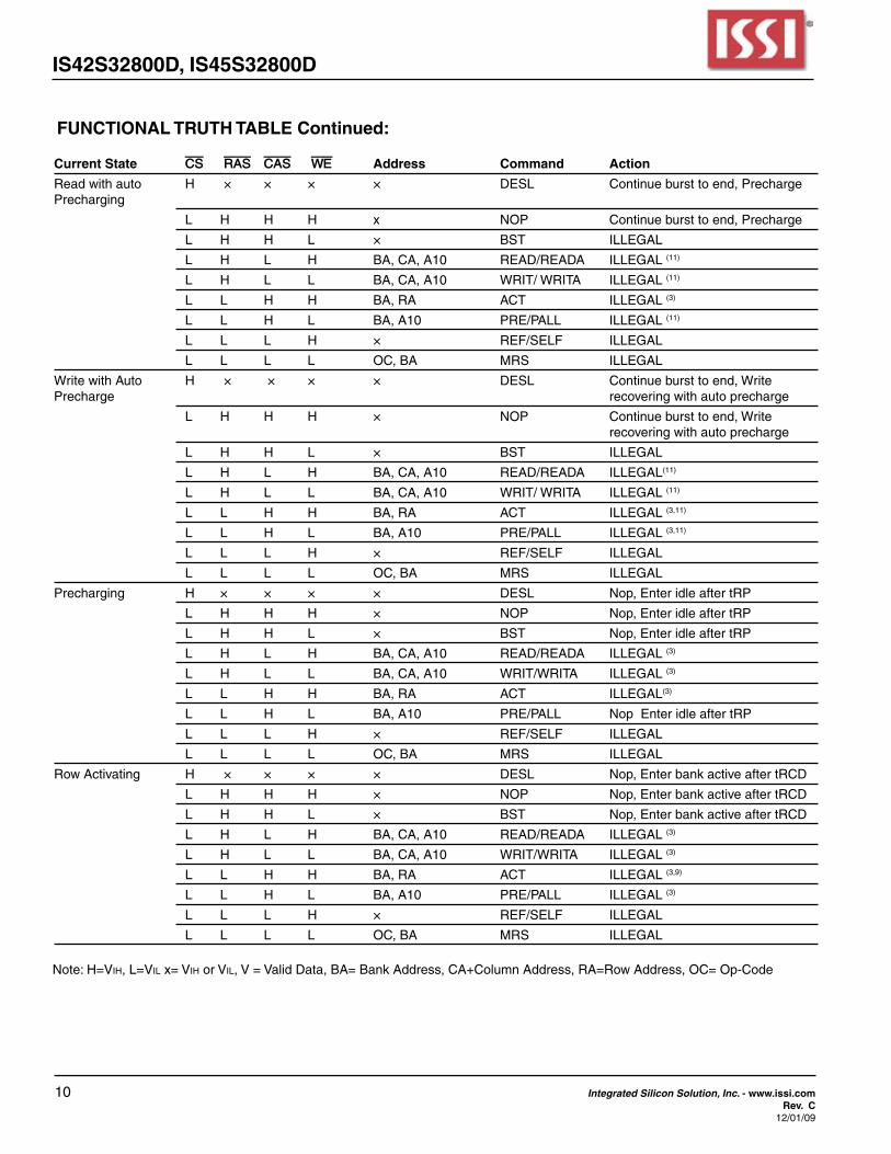
Current State CS RAS CAS WE Address Command Action
Readwithauto H × × × × DESL Continuebursttoend,PrechargePrecharging
L H H H x NOP Continuebursttoend,Precharge
L H H L × BST ILLEGAL
L H L H BA,CA,A10 READ/READA ILLEGAL(11)
L H L L BA,CA,A10 WRIT/WRITA ILLEGAL(11)
L L H H BA,RA ACT ILLEGAL(3)
L L H L BA,A10 PRE/PALL ILLEGAL(11)
L L L H × REF/SELF ILLEGAL
L L L L OC,BA MRS ILLEGAL
WritewithAuto H × × × × DESL Continuebursttoend,Write Precharge recoveringwithautoprecharge
L H H H × NOP Continuebursttoend,Write recovering with auto precharge
L H H L × BST ILLEGAL
L H L H BA,CA,A10 READ/READA ILLEGAL(11)
L H L L BA,CA,A10 WRIT/WRITA ILLEGAL(11)
L L H H BA,RA ACT ILLEGAL(3,11)
L L H L BA,A10 PRE/PALL ILLEGAL(3,11)
L L L H × REF/SELF ILLEGAL
L L L L OC,BA MRS ILLEGAL
Precharging H × × × × DESL Nop,EnteridleaftertRP
L H H H × NOP Nop,EnteridleaftertRP
L H H L × BST Nop,EnteridleaftertRP
L H L H BA,CA,A10 READ/READA ILLEGAL(3)
L H L L BA,CA,A10 WRIT/WRITA ILLEGAL(3)
L L H H BA,RA ACT ILLEGAL(3)
L L H L BA,A10 PRE/PALL NopEnteridleaftertRP
L L L H × REF/SELF ILLEGAL
L L L L OC,BA MRS ILLEGAL
RowActivating H × × × × DESL Nop,EnterbankactiveaftertRCD
L H H H × NOP Nop,EnterbankactiveaftertRCD
L H H L × BST Nop,EnterbankactiveaftertRCD
L H L H BA,CA,A10 READ/READA ILLEGAL(3)
L H L L BA,CA,A10 WRIT/WRITA ILLEGAL(3)
L L H H BA,RA ACT ILLEGAL(3,9)
L L H L BA,A10 PRE/PALL ILLEGAL(3)
L L L H × REF/SELF ILLEGAL
L L L L OC,BA MRS ILLEGAL
FUNCTIONAL TRUTH TABLE Continued:
Note:H=Vih,L=Vilx=VihorVil,V=ValidData,BA=BankAddress,CA+ColumnAddress,RA=RowAddress,OC=Op-Code
IS42S32800D, IS45S32800D
Integrated Silicon Solution, Inc. - www.issi.com 11Rev. C12/01/09
Current State CS RAS CAS WE Address Command Action
WriteRecovering H × × × × DESL Nop,EnterrowactiveaftertDPL
L H H H × NOP Nop,EnterrowactiveaftertDPL
L H H L × BST Nop,EnterrowactiveaftertDPL
L H L H BA,CA,A10 READ/READA Beginread(8)
L H L L BA,CA,A10 WRIT/WRITA Beginnewwrite
L L H H BA,RA ACT ILLEGAL(3)
L L H L BA,A10 PRE/PALL ILLEGAL(3)
L L L H × REF/SELF ILLEGAL
L L L L OC,BA MRS ILLEGAL
WriteRecovering H × × × × DESL Nop,EnterprechargeaftertDPL
withAuto L H H H × NOP Nop,EnterprechargeaftertDPL
Precharge L H H L × BST Nop,EnterrowactiveaftertDPL
L H L H BA,CA,A10 READ/READA ILLEGAL(3,8,11)
L H L L BA,CA,A10 WRIT/WRITA ILLEGAL(3,11)
L L H H BA,RA ACT ILLEGAL(3,11)
L L H L BA,A10 PRE/PALL ILLEGAL(3,11)
L L L H × REF/SELF ILLEGAL
L L L L OC,BA MRS ILLEGAL
Refresh H × × × × DESL Nop,EnteridleaftertRC
L H H × × NOP/BST Nop,EnteridleaftertRC
L H L H BA,CA,A10 READ/READA ILLEGAL
L H L L BA,CA,A10 WRIT/WRITA ILLEGAL
L L H H BA,RA ACT ILLEGAL
L L H L BA,A10 PRE/PALL ILLEGAL
L L L H × REF/SELF ILLEGAL
L L L L OC,BA MRS ILLEGAL
ModeRegister H × × × × DESL Nop,Enteridleafter2clocks
Accessing L H H H × NOP Nop,Enteridleafter2clocks
L H H L × BST ILLEGAL
L H L × BA,CA,A10 READ/WRITE ILLEGAL
L L × × BA,RA ACT/PRE/PALL ILLEGAL REF/MRS
FUNCTIONAL TRUTH TABLE Continued:
Note:H=Vih,L=Vilx=VihorVil,V=ValidData,BA=BankAddress,CA+ColumnAddress,RA=RowAddress,OC=Op-Code
Notes:1.AllentriesassumethatCKEisactive(CKEn-1=CKEn=H).2.Ifbothbanksareidle,andCKEisinactive(Low),thedevicewillenterPowerDownmode.AllinputbuffersexceptCKEwillbe
disabled.3.Illegaltobankinspecifiedstates;FunctionmaybelegalinthebankindicatedbyBankAddress(BA),dependingonthestateof
that bank.4.Ifbothbanksareidle,andCKEisinactive(Low),thedevicewillenterSelf-Refreshmode.AllinputbuffersexceptCKEwillbe
disabled.5.IllegaliftRCDisnotsatisfied.6.IllegaliftRASisnotsatisfied.7.Mustsatisfyburstinterruptcondition.8.Mustsatisfybuscontention,busturnaround,and/orwriterecoveryrequirements.9.Mustmaskprecedingdatawhichdon’tsatisfytDPL.10.IllegaliftRRDisnotsatisfied.11. Illegal for single bank, but legal for other banks.
12 Integrated Silicon Solution, Inc. - www.issi.comRev. C
12/01/09
IS42S32800D, IS45S32800D
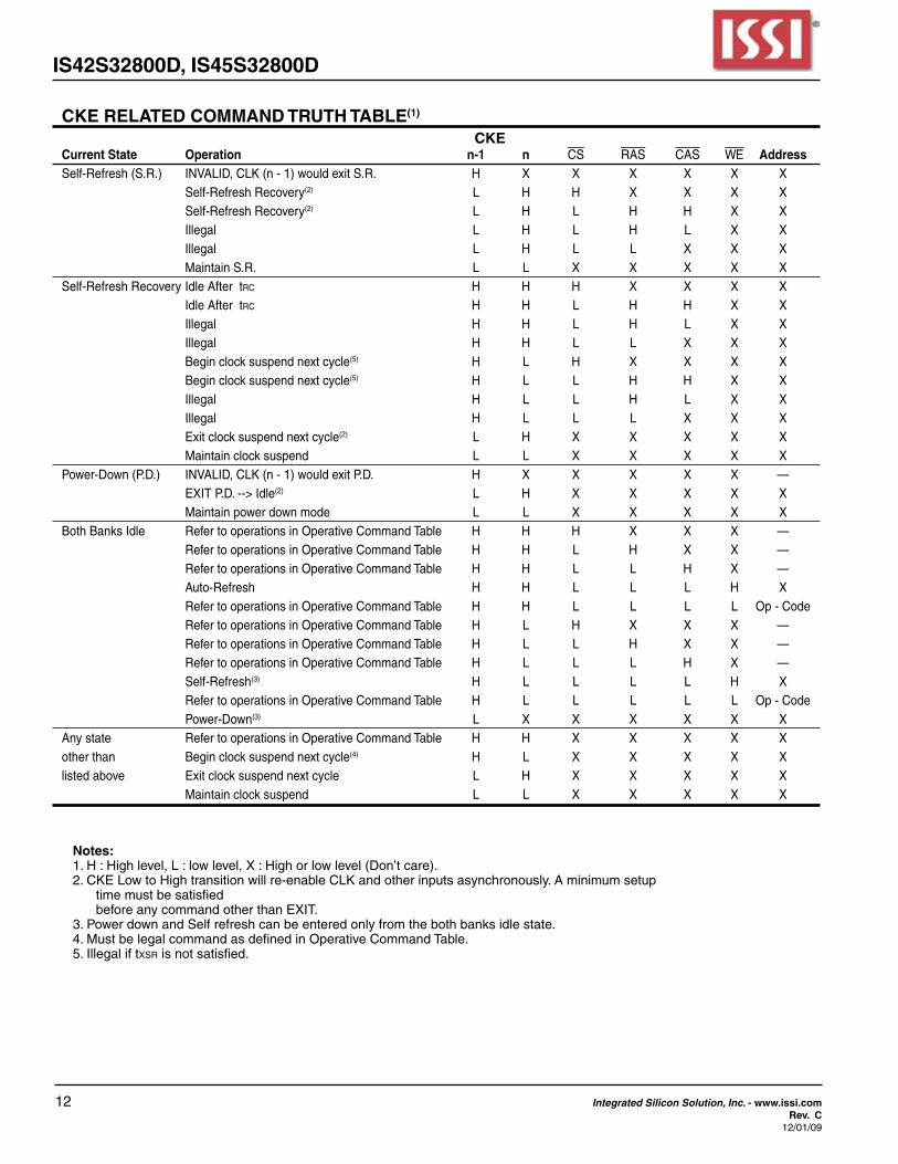
CKE RELATED COMMAND TRUTH TABLE(1)
CKE Current State Operation n-1 n CS RAS CAS WE AddressSelf-Refresh(S.R.) INVALID,CLK(n-1)wouldexitS.R. H X X X X X X Self-RefreshRecovery(2) L H H X X X X Self-RefreshRecovery(2) L H L H H X X Illegal L H L H L X X Illegal L H L L X X X MaintainS.R. L L X X X X XSelf-RefreshRecoveryIdleAftertrc H H H X X X X Idle After trc H H L H H X X Illegal H H L H L X X Illegal H H L L X X X Beginclocksuspendnextcycle(5) H L H X X X X Beginclocksuspendnextcycle(5) H L L H H X X Illegal H L L H L X X Illegal H L L L X X X Exitclocksuspendnextcycle(2) L H X X X X X Maintainclocksuspend L L X X X X XPower-Down(P.D.) INVALID,CLK(n-1)wouldexitP.D. H X X X X X — EXITP.D.-->Idle(2) L H X X X X X Maintainpowerdownmode L L X X X X XBothBanksIdle RefertooperationsinOperativeCommandTable H H H X X X — RefertooperationsinOperativeCommandTable H H L H X X — RefertooperationsinOperativeCommandTable H H L L H X — Auto-Refresh H H L L L H X RefertooperationsinOperativeCommandTable H H L L L L Op-Code RefertooperationsinOperativeCommandTable H L H X X X — RefertooperationsinOperativeCommandTable H L L H X X — RefertooperationsinOperativeCommandTable H L L L H X — Self-Refresh(3) H L L L L H X RefertooperationsinOperativeCommandTable H L L L L L Op-Code Power-Down(3) L X X X X X XAnystate RefertooperationsinOperativeCommandTable H H X X X X Xotherthan Beginclocksuspendnextcycle(4) H L X X X X Xlistedabove Exitclocksuspendnextcycle L H X X X X X Maintainclocksuspend L L X X X X X
Notes:1.H:Highlevel,L:lowlevel,X:Highorlowlevel(Don’tcare).2.CKELowtoHightransitionwillre-enableCLKandotherinputsasynchronously.Aminimumsetup
time must be satisfied beforeanycommandotherthanEXIT.3.PowerdownandSelfrefreshcanbeenteredonlyfromthebothbanksidlestate.4.MustbelegalcommandasdefinedinOperativeCommandTable.5.Illegaliftxsr is not satisfied.
IS42S32800D, IS45S32800D
Integrated Silicon Solution, Inc. - www.issi.com 13Rev. C12/01/09
ModeRegister
SetIDLE
SelfRefresh
CBR(Auto)Refresh
RowActive
ActivePowerDown
PowerDown
WRITEWRITE
SUSPENDREAD
READSUSPEND
WRITEASUSPEND
WRITEA READAREADA
SUSPEND
POWERON
Precharge
Automaticsequence
ManualInput
SELF
SELFexit
REFMRS
ACT
CKE
CKE
CKE
CKE
BST
Read
Write
Write
Precharge
RR
E(Precharge termination) PR
E(P
rech
arge
term
inat
ion)
Writ
ew
ithA
uto
Pre
char
ge Readw
ith
AutoP
recharge
Read
Write
BST
CKE
CKECKE
CKE
CKE
CKECKE
CKE
Read
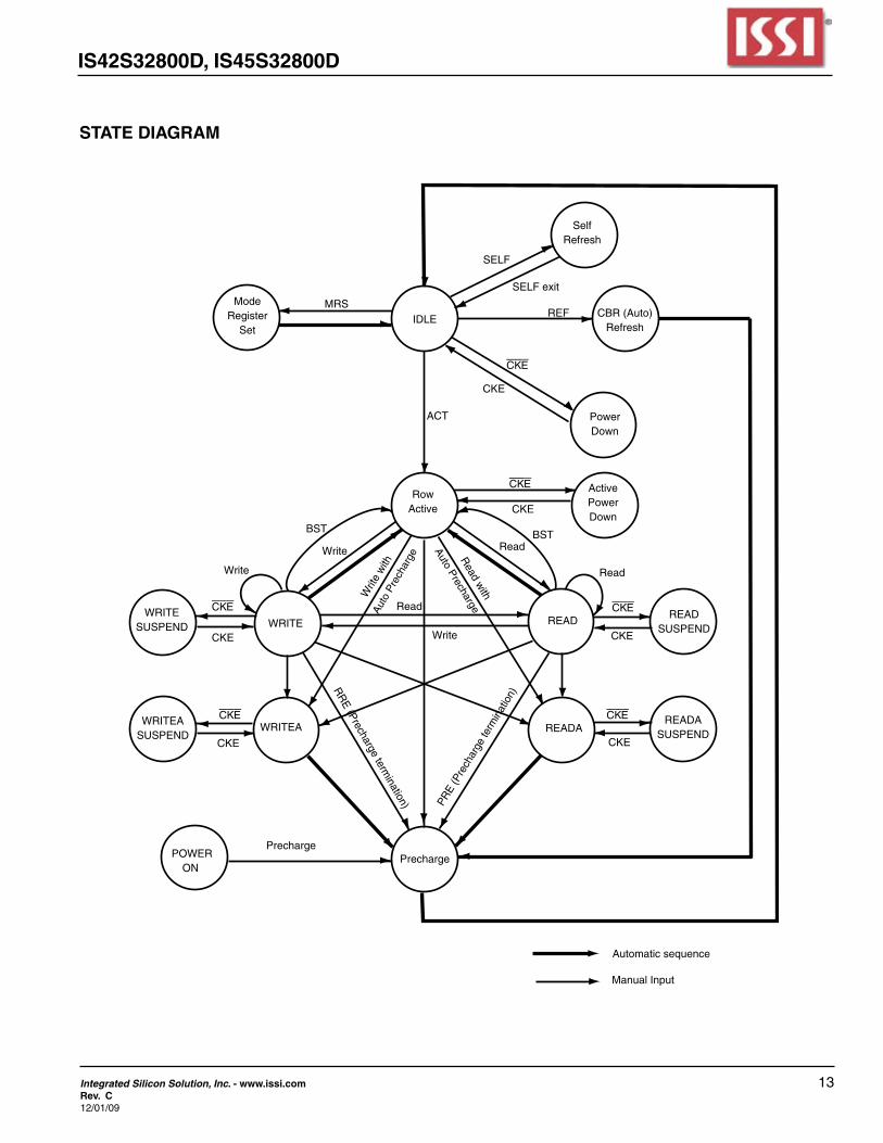
STATE DIAGRAM
14 Integrated Silicon Solution, Inc. - www.issi.comRev. C
12/01/09
IS42S32800D, IS45S32800D
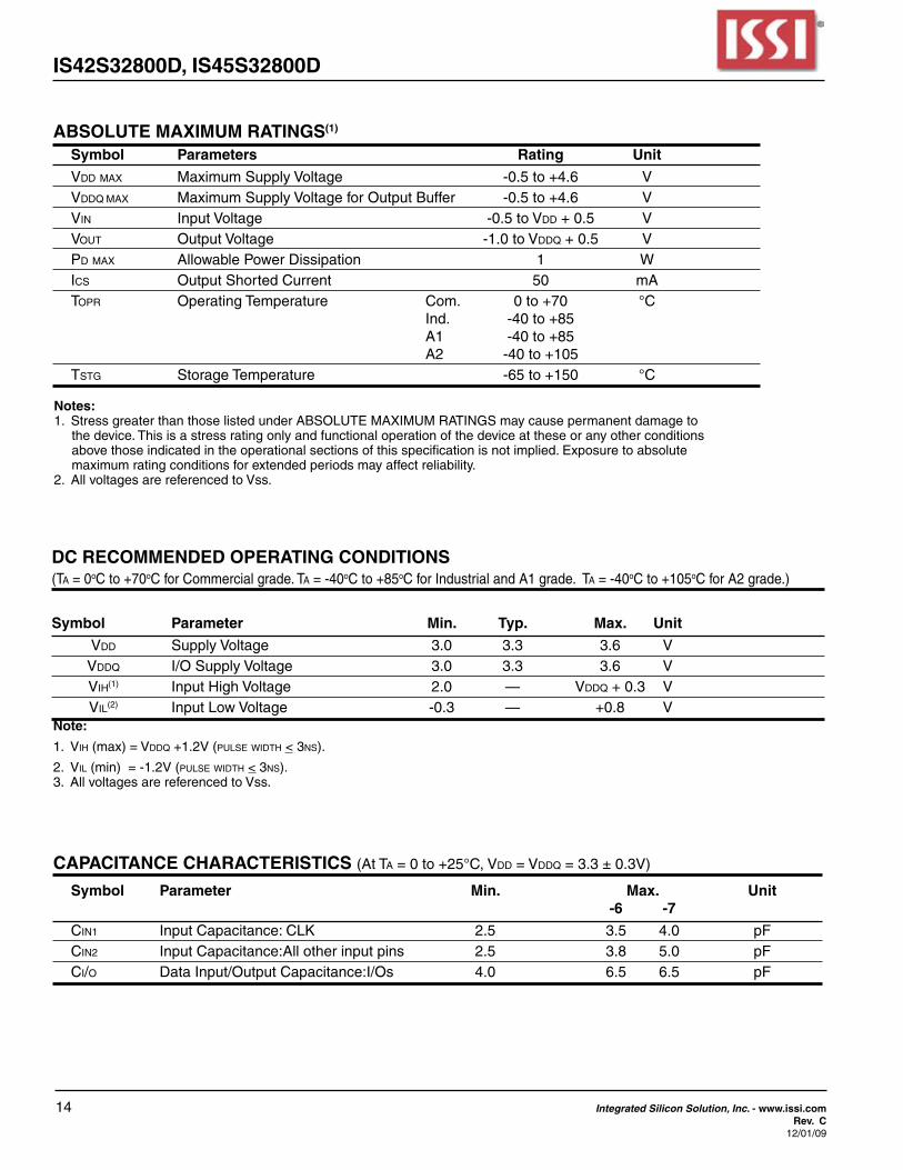
ABSOLUTE MAXIMUM RATINGS(1)
Symbol Parameters Rating Unit
Vdd max MaximumSupplyVoltage -0.5to+4.6 V Vddq max MaximumSupplyVoltageforOutputBuffer -0.5to+4.6 V Vin InputVoltage -0.5toVdd+0.5 V Vout OutputVoltage -1.0toVddq+0.5 V Pd max AllowablePowerDissipation 1 W Ics outputShortedCurrent 50 mA Topr operatingTemperature Com. 0to+70 °C Ind. -40to+85 A1 -40to+85 A2 -40to+105 Tstg StorageTemperature -65to+150 °C
DC RECOMMENDED OPERATING CONDITIONS (Ta=0oC to +70oCforCommercialgrade.Ta=-40oCto+85oCforIndustrialandA1grade.Ta=-40oCto+105oCforA2grade.)
Symbol Parameter Min. Typ. Max. Unit
Vdd SupplyVoltage 3.0 3.3 3.6 V Vddq I/OSupplyVoltage 3.0 3.3 3.6 V Vih(1) InputHighVoltage 2.0 — Vddq +0.3 V Vil(2) InputLowVoltage -0.3 — +0.8 V
CAPACITANCE CHARACTERISTICS (AtTa=0to+25°C,Vdd=Vddq =3.3±0.3V)
Symbol Parameter Min. Max. Unit -6 -7
Cin1 InputCapacitance:CLK 2.5 3.5 4.0 pF Cin2 InputCapacitance:Allotherinputpins 2.5 3.8 5.0 pF Ci/o DataInput/OutputCapacitance:I/Os 4.0 6.5 6.5 pF
Note:
1.Vih (max)=Vddq +1.2V (pulse width < 3ns).
2.Vil(min)=-1.2V (pulse width < 3ns).3. AllvoltagesarereferencedtoVss.
Notes:1. StressgreaterthanthoselistedunderABSOLUTEMAXIMUMRATINGSmaycausepermanentdamageto
thedevice.Thisisastressratingonlyandfunctionaloperationofthedeviceattheseoranyotherconditionsabovethoseindicatedintheoperationalsectionsofthisspecificationisnotimplied.Exposuretoabsolutemaximumratingconditionsforextendedperiodsmayaffectreliability.
2. AllvoltagesarereferencedtoVss.
IS42S32800D, IS45S32800D
Integrated Silicon Solution, Inc. - www.issi.com 15Rev. C12/01/09
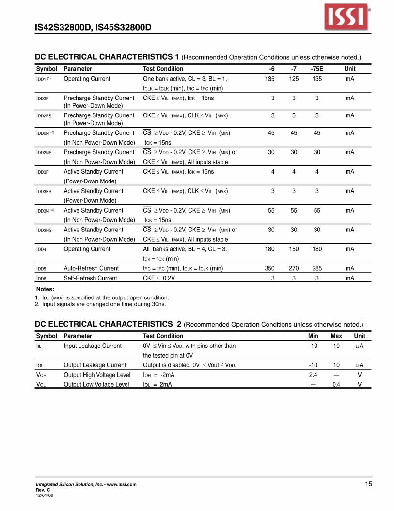
DC ELECTRICAL CHARACTERISTICS 1 (RecommendedOperationConditionsunlessotherwisenoted.)
Symbol Parameter Test Condition -6 -7 -75E Unit
idd1 (1) OperatingCurrent Onebankactive,CL=3,BL=1, 135 125 135 mA
tclk=tclk(min),trc=trc(min)
idd2p PrechargeStandbyCurrent CKE≤ Vil (max),tck=15ns 3 3 3 mA (InPower-DownMode)
idd2ps PrechargeStandbyCurrent CKE≤ Vil (max),CLK≤ Vil (max) 3 3 3 mA (InPower-DownMode)
idd2n (2) PrechargeStandbyCurrent CS ≥ Vdd-0.2V,CKE≥ Vih (min) 45 45 45 mA
(InNonPower-DownMode) tck=15ns
Idd2ns PrechargeStandbyCurrent CS ≥ Vdd-0.2V,CKE≥ Vih (min)or 30 30 30 mA
(InNonPower-DownMode) CKE≤ Vil (max),Allinputsstable
Idd3p ActiveStandbyCurrent CKE≤ Vil (max),tck=15ns 4 4 4 mA
(Power-DownMode)
Idd3ps ActiveStandbyCurrent CKE≤ Vil (max),CLK≤ Vil (max) 3 3 3 mA
(Power-DownMode)
idd3n (2) Active Standby Current CS ≥ Vdd-0.2V,CKE≥ Vih (min) 55 55 55 mA
(InNonPower-DownMode) tck=15ns
Idd3ns Active Standby Current CS ≥ Vdd-0.2V,CKE≥ Vih (min)or 30 30 30 mA
(InNonPower-DownMode) CKE≤ Vil (max),Allinputsstable
idd4 OperatingCurrent Allbanksactive,BL=4,CL=3, 180 150 180 mA
tck=tck(min)
idd5 Auto-RefreshCurrent trc=trc(min),tclk=tclk(min) 350 270 285 mA
idd6 Self-RefreshCurrent CKE≤ 0.2V 3 3 3 mA
Notes:1. Idd (max)isspecifiedattheoutputopencondition.2. Inputsignalsarechangedonetimeduring30ns.
DC ELECTRICAL CHARACTERISTICS 2 (RecommendedOperationConditionsunlessotherwisenoted.)
Symbol Parameter Test Condition Min Max Unit
iil InputLeakageCurrent 0V≤Vin≤Vdd, with pins other than -10 10 µA
thetestedpinat0V
iol OutputLeakageCurrent Outputisdisabled,0V≤Vout≤Vdd, -10 10 µA
Voh OutputHighVoltageLevel Ioh=-2mA 2.4 — V
Vol OutputLowVoltageLevel Iol=2mA — 0.4 V
16 Integrated Silicon Solution, Inc. - www.issi.comRev. C
12/01/09
IS42S32800D, IS45S32800D
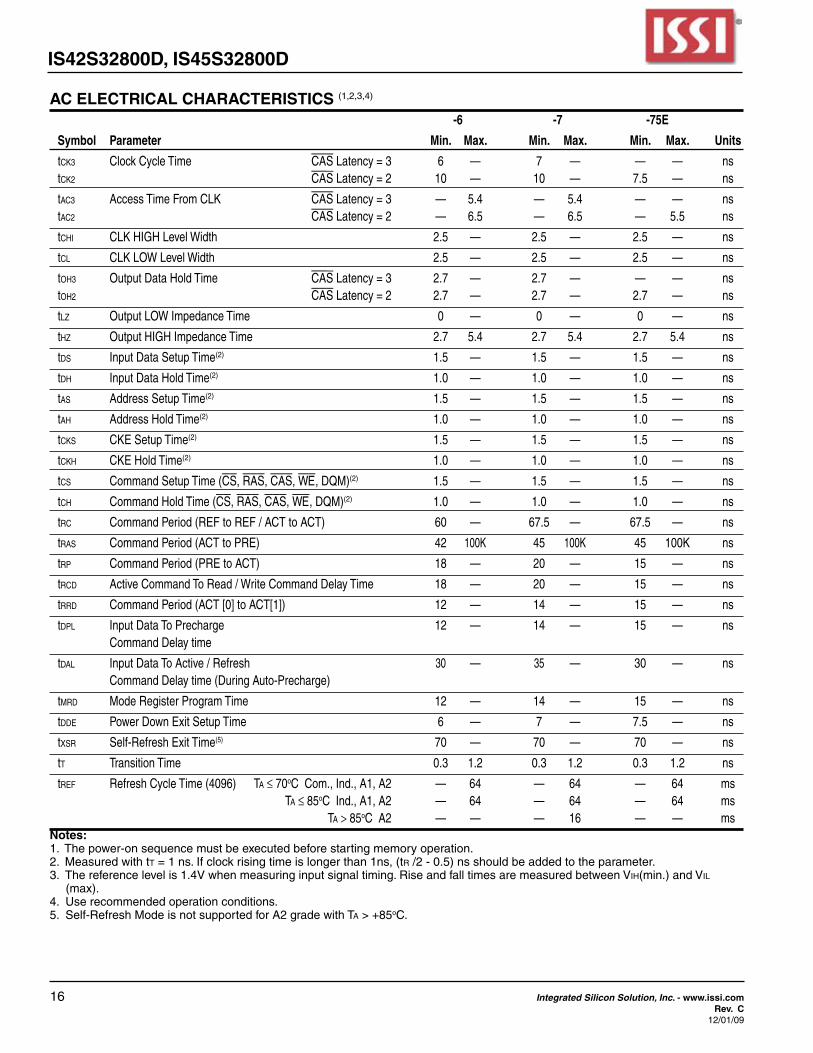
AC ELECTRICAL CHARACTERISTICS (1,2,3,4)
-6 -7 -75E
Symbol Parameter Min. Max. Min. Max. Min. Max. Units
tck3 ClockCycleTime CASLatency=3 6 — 7 — — — ns tck2 CASLatency=2 10 — 10 — 7.5 — ns
tac3 AccessTimeFromCLK CASLatency=3 — 5.4 — 5.4 — — ns tac2 CASLatency=2 — 6.5 — 6.5 — 5.5 ns
tchi CLKHIGHLevelWidth 2.5 — 2.5 — 2.5 — ns
tcl CLKLOWLevelWidth 2.5 — 2.5 — 2.5 — ns
toh3 OutputDataHoldTime CASLatency=3 2.7 — 2.7 — — — ns toh2 CAS Latency=2 2.7 — 2.7 — 2.7 — ns
tlz OutputLOWImpedanceTime 0 — 0 — 0 — ns
thz OutputHIGHImpedanceTime 2.7 5.4 2.7 5.4 2.7 5.4 ns
tds InputDataSetupTime(2) 1.5 — 1.5 — 1.5 — ns
tdh InputDataHoldTime(2) 1.0 — 1.0 — 1.0 — ns
tas AddressSetupTime(2) 1.5 — 1.5 — 1.5 — ns
tah AddressHoldTime(2) 1.0 — 1.0 — 1.0 — ns
tcks CKESetupTime(2) 1.5 — 1.5 — 1.5 — ns
tckh CKEHoldTime(2) 1.0 — 1.0 — 1.0 — ns
tcs CommandSetupTime(CS, RAS, CAS, WE,DQM)(2) 1.5 — 1.5 — 1.5 — ns
tch CommandHoldTime(CS, RAS, CAS, WE,DQM)(2) 1.0 — 1.0 — 1.0 — ns
trc CommandPeriod(REFtoREF/ACTtoACT) 60 — 67.5 — 67.5 — ns
tras CommandPeriod(ACTtoPRE) 42 100K 45 100K 45 100K ns
trp CommandPeriod(PREtoACT) 18 — 20 — 15 — ns
trcd ActiveCommandToRead/WriteCommandDelayTime 18 — 20 — 15 — ns
trrd CommandPeriod(ACT[0]toACT[1]) 12 — 14 — 15 — ns
tdpl InputDataToPrecharge 12 — 14 — 15 — ns CommandDelaytime
tdal InputDataToActive/Refresh 30 — 35 — 30 — ns CommandDelaytime(DuringAuto-Precharge)
tmrd ModeRegisterProgramTime 12 — 14 — 15 — ns
tdde PowerDownExitSetupTime 6 — 7 — 7.5 — ns
txsr Self-RefreshExitTime(5) 70 — 70 — 70 — ns
tt TransitionTime 0.3 1.2 0.3 1.2 0.3 1.2 ns
tref RefreshCycleTime(4096) Ta ≤ 70oC Com., Ind., A1, A2 — 64 — 64 — 64 ms Ta ≤85oC Ind., A1, A2 — 64 — 64 — 64 ms Ta >85oC A2 — — — 16 — — msNotes:1. Thepower-onsequencemustbeexecutedbeforestartingmemoryoperation.2. measured with tt =1ns.Ifclockrisingtimeislongerthan1ns,(tr/2-0.5)nsshouldbeaddedtotheparameter.3.Thereferencelevelis1.4Vwhenmeasuringinputsignaltiming.RiseandfalltimesaremeasuredbetweenVih(min.)andVil
(max).4.Userecommendedoperationconditions.5.Self-RefreshModeisnotsupportedforA2gradewithTa>+85oC.
IS42S32800D, IS45S32800D
Integrated Silicon Solution, Inc. - www.issi.com 17Rev. C12/01/09
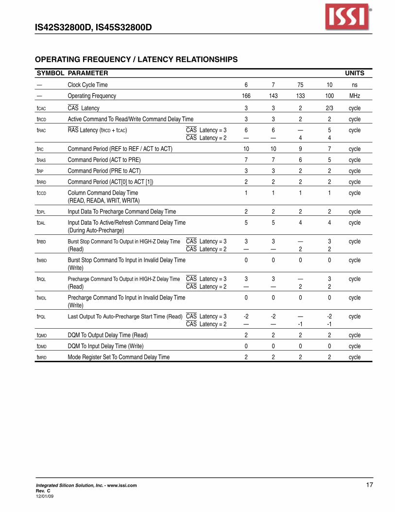
OPERATING FREQUENCY / LATENCY RELATIONSHIPS
SYMBOL PARAMETER UNITS
— ClockCycleTime 6 7 75 10 ns
— OperatingFrequency 166 143 133 100 MHz
tcac CASLatency 3 3 2 2/3 cycle
trcd ActiveCommandToRead/WriteCommandDelayTime 3 3 2 2 cycle
trac RASLatency(trcd + tcac) CASLatency=3 6 6 — 5 cycle CASLatency=2 — — 4 4
trc CommandPeriod(REFtoREF/ACTtoACT) 10 10 9 7 cycle
tras CommandPeriod(ACTtoPRE) 7 7 6 5 cycle
trp CommandPeriod(PREtoACT) 3 3 2 2 cycle
trrd CommandPeriod(ACT[0]toACT[1]) 2 2 2 2 cycle
tccd ColumnCommandDelayTime 1 1 1 1 cycle (READ,READA,WRIT,WRITA)
tdpl InputDataToPrechargeCommandDelayTime 2 2 2 2 cycle
tdal InputDataToActive/RefreshCommandDelayTime 5 5 4 4 cycle (DuringAuto-Precharge)
trbd BurstStopCommandToOutputinHIGH-ZDelayTime CASLatency=3 3 3 — 3 cycle (Read) CASLatency=2 — — 2 2
twbd BurstStopCommandToInputinInvalidDelayTime 0 0 0 0 cycle (Write)
trql PrechargeCommandToOutputinHIGH-ZDelayTime CASLatency=3 3 3 — 3 cycle (Read) CASLatency=2 — — 2 2
twdl PrechargeCommandToInputinInvalidDelayTime 0 0 0 0 cycle (Write)
tpql LastOutputToAuto-PrechargeStartTime(Read) CASLatency=3 -2 -2 — -2 cycle CASLatency=2 — — -1 -1
tqmd DQMToOutputDelayTime(Read) 2 2 2 2 cycle
tdmd DQMToInputDelayTime(Write) 0 0 0 0 cycle
tmrd ModeRegisterSetToCommandDelayTime 2 2 2 2 cycle
18 Integrated Silicon Solution, Inc. - www.issi.comRev. C
12/01/09
IS42S32800D, IS45S32800D
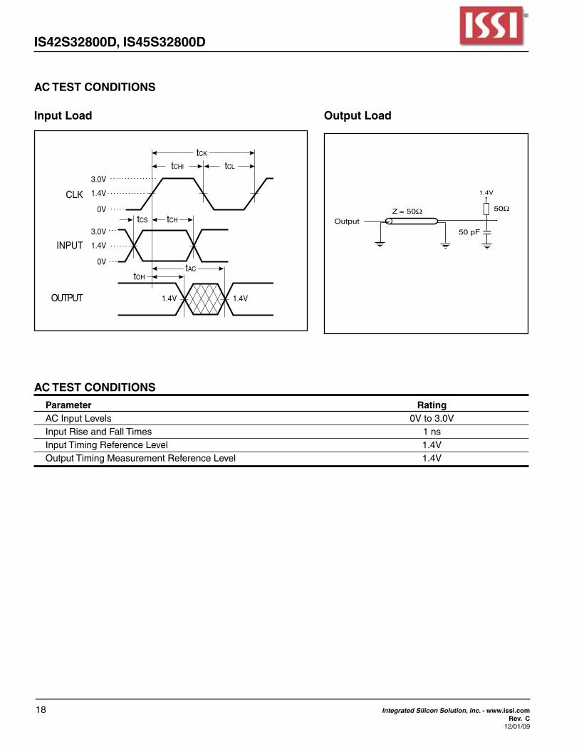
AC TEST CONDITIONS
Input Load Output Load
Output Z = 50Ω
50 pF
1.4V
50Ω
3.0V
1.4V
0V
CLK
INPUT
OUTPUT
tCHI
tCH
tACtOH
tCS
tCK
tCL
3.0V
1.4V
1.4V 1.4V
0V
AC TEST CONDITIONS
Parameter Rating ACInputLevels 0Vto3.0V InputRiseandFallTimes 1ns InputTimingReferenceLevel 1.4V OutputTimingMeasurementReferenceLevel 1.4V
IS42S32800D, IS45S32800D
Integrated Silicon Solution, Inc. - www.issi.com 19Rev. C12/01/09
FUNCTIONAL DESCRIPTIONReadandwriteaccessestotheSDRAMareburstoriented;accesses start at a selected location and continue for a programmed number of locations in a programmed sequence.AccessesbeginwiththeregistrationofanAC-TIVEcommandwhichisthenfollowedbyaREADorWRITEcommand.TheaddressbitsregisteredcoincidentwiththeACTIVEcommandareusedtoselectthebankandrowtobe accessed (BA0andBA1selectthebank,A0-A11selecttherow).TheaddressbitsA0-A8 registered coincident with the READorWRITEcommandareusedtoselectthestartingcolumn location for the burst access.
Prior to normal operation, the SDRAM must be initial-ized.Thefollowingsectionsprovidedetailedinformationcoveringdeviceinitialization,registerdefinition,command descriptions and device operation.
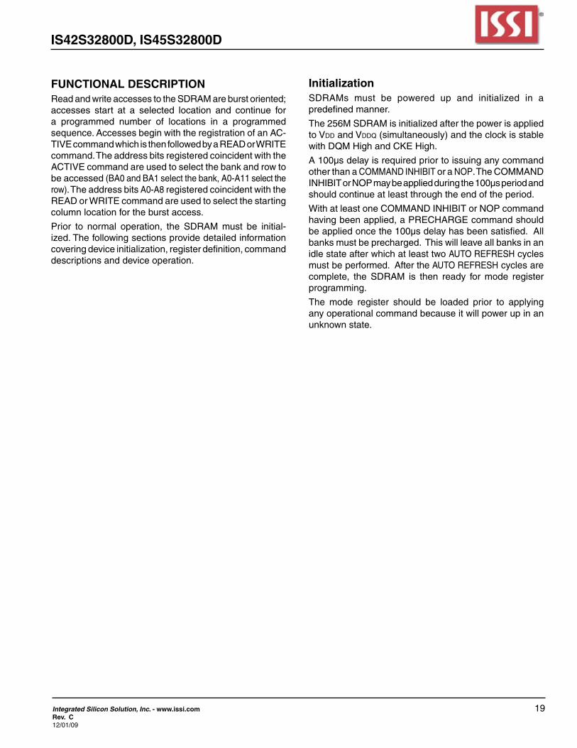
InitializationSDRAMs must be powered up and initialized in a predefined manner.
The256MSDRAMisinitializedafterthepowerisappliedtoVddandVddq(simultaneously)andtheclockisstablewithDQMHighandCKEHigh.
A100µsdelayisrequiredpriortoissuinganycommandother than a COMMANDINHIBIT or a NOP.TheCOMMANDINHIBITorNOPmaybeappliedduringthe100µsperiodandshould continue at least through the end of the period.
WithatleastoneCOMMANDINHIBITorNOPcommandhavingbeenapplied,aPRECHARGEcommandshouldbe applied once the 100µs delay has been satisfied. All banksmustbeprecharged.Thiswillleaveallbanksinanidle state after which at least two AUTOREFRESH cycles must be performed. After the AUTOREFRESH cycles are complete, the SDRAM is then ready for mode registerprogramming.
The mode register should be loaded prior to applyingany operational command because it will power up in an unknown state.
20 Integrated Silicon Solution, Inc. - www.issi.comRev. C
12/01/09
IS42S32800D, IS45S32800D
INITIALIzE AND LOAD MODE REGISTER(1)
DON'T CARE
CLK
CKE
COMMAND
DQM0-DQM3
A0-A9, A11
A10
BA0, BA1
DQ
tCH tCLtCK
tCMH tCMS tCMH tCMS tCMH tCMS
tCKS tCKH
T0 T1 Tn+1 To+1 Tp+1 Tp+2 Tp+3
tMRDtRCtRCtRP
ROW
ROW
BANK
tAS tAH
tAS tAH
CODE
CODEALL BANKS
SINGLE BANK
ALL BANKS
AUTOREFRESH
AUTOREFRESH
Load MODEREGISTER
T = 100µs Min.
Power-up: VCC
and CLK stablePrechargeall banks
AUTO REFRESH Program MODE REGISTER
NOP PRECHARGE NOP NOP NOP ACTIVE
T
(2, 3, 4)AUTO REFRESH
CODE
tAS tAH
Notes:1. If CSisHighatclockHightime,allcommandsappliedareNOP.2.TheModeregistermaybeloadedpriortotheAuto-Refreshcyclesifdesired.3.JEDECandPC100specifythreeclocks.4.OutputsareguaranteedHigh-Zafterthecommandisissued.
IS42S32800D, IS45S32800D
Integrated Silicon Solution, Inc. - www.issi.com 21Rev. C12/01/09
AUTO-REFRESH CYCLE
Notes:1. CASlatency=2,3
tRP tRC tRC
DON'T CARE
CLK
CKE
COMMAND
DQM0 - DQM3
A0-A9, A11
A10
BA0, BA1
DQ
tAS tAH
tCHtCLtCK
tCMS tCMH
tCKS tCKH
T0 T1 T2 Tn+1 To+1
ALL BANKS
SINGLE BANK
BANK(s)
ROW
ROW
BANK
High-Z
PRECHARGE NOP NOP NOP ACTIVEAutoRefresh
AutoRefresh
22 Integrated Silicon Solution, Inc. - www.issi.comRev. C
12/01/09
IS42S32800D, IS45S32800D
SELF-REFRESH CYCLE
CLK
CKE
COMMAND
DQM0 - DQM3
A0-A9, A11
A10
BA0, BA1
DQ
tAS tAH
BANK
tCLtCHtCK
tCMS tCMH
tCKS tCKH
ALL BANKS
SINGLE BANK
tCKS
Precharge allactive banks
CLK stable prior to exitingself refresh mode
Enter selfrefresh mode
Exit self refresh mode(Restart refresh time base)
T0 T1 T2 Tn+1 To+1 To+2
High-Z
AutoRefresh
AutoRefreshPRECHARGE NOP NOP NOP
tCKS
≥ tRAS
tRP tXSR
DON'T CARE
Note:1.Self-RefreshModeisnotsupportedforA2gradewithTa>+85oC.
IS42S32800D, IS45S32800D
Integrated Silicon Solution, Inc. - www.issi.com 23Rev. C12/01/09
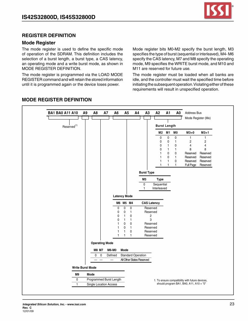
REGISTER DEFINITION
Mode RegisterThemode register isused todefine thespecificmodeofoperationof theSDRAM.Thisdefinition includestheselection of a burst length, a burst type, a CAS latency, an operating mode and a write burst mode, as shown in MODEREGISTERDEFINITION.
ThemoderegisterisprogrammedviatheLOADMODEREGISTERcommandandwillretainthestoredinformationuntil it is programmed again or the device loses power.
Mode register bitsM0-M2specify theburst length,M3specifies the type of burst (sequentialorinterleaved),M4-M6specifytheCASlatency,M7andM8specifytheoperatingmode,M9specifiestheWRITEburstmode,andM10andM11arereservedforfutureuse.
Themode registermustbe loadedwhenallbanksareidle, and the controller must wait the specified time before initiatingthesubsequentoperation.Violatingeitheroftheserequirementswillresultinunspecifiedoperation.
MODE REGISTER DEFINITION
Latency Mode
M6 M5 M4 CAS Latency
0 0 0 Reserved 0 0 1 Reserved 0 1 0 2 0 1 1 3 1 0 0 Reserved 1 0 1 Reserved 1 1 0 Reserved 1 1 1 Reserved
1. To ensure compatibility with future devices,should program BA1, BA0, A11, A10 = "0"
Write Burst Mode
M9 Mode
0 Programmed Burst Length
1 Single Location Access
Operating Mode
M8 M7 M6-M0 Mode
0 0 Defined Standard Operation — — — All Other States Reserved
Burst Type
M3 Type
0 Sequential 1 Interleaved
Burst Length
M2 M1 M0 M3=0 M3=1
0 0 0 1 1 0 0 1 2 2 0 1 0 4 4 0 1 1 8 8 1 0 0 Reserved Reserved 1 0 1 Reserved Reserved 1 1 0 Reserved Reserved 1 1 1 Full Page Reserved
Reserved
Address Bus
Mode Register (Mx)
(1)
BA1 BA0 A11 A10 A9 A8 A7 A6 A5 A4 A3 A2 A1 A0
24 Integrated Silicon Solution, Inc. - www.issi.comRev. C
12/01/09
IS42S32800D, IS45S32800D
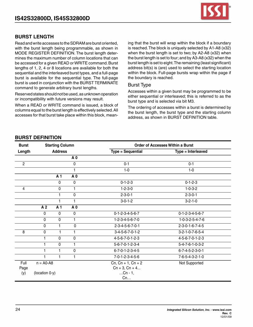
BURST DEFINITION
Burst Starting Column Order of Accesses Within a Burst
Length Address Type = Sequential Type = Interleaved
A 0
2 0 0-1 0-1
1 1-0 1-0
A 1 A 0
0 0 0-1-2-3 0-1-2-3
4 0 1 1-2-3-0 1-0-3-2
1 0 2-3-0-1 2-3-0-1
1 1 3-0-1-2 3-2-1-0
A 2 A 1 A 0
0 0 0 0-1-2-3-4-5-6-7 0-1-2-3-4-5-6-7
0 0 1 1-2-3-4-5-6-7-0 1-0-3-2-5-4-7-6
0 1 0 2-3-4-5-6-7-0-1 2-3-0-1-6-7-4-5
8 0 1 1 3-4-5-6-7-0-1-2 3-2-1-0-7-6-5-4
1 0 0 4-5-6-7-0-1-2-3 4-5-6-7-0-1-2-3
1 0 1 5-6-7-0-1-2-3-4 5-4-7-6-1-0-3-2
1 1 0 6-7-0-1-2-3-4-5 6-7-4-5-2-3-0-1
1 1 1 7-0-1-2-3-4-5-6 7-6-5-4-3-2-1-0
Full n=A0-A8 Cn,Cn+1,Cn+2 NotSupported Page Cn+3,Cn+4... (y) (location0-y) …Cn-1, Cn…
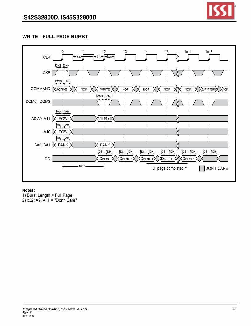
BURST LENGTHReadandwriteaccessestotheSDRAMareburstoriented,with the burst length being programmable, as shown in MODEREGISTERDEFINITION.Theburstlengthdeter-minesthemaximumnumberofcolumnlocationsthatcanbeaccessedforagivenREADorWRITEcommand.Burstlengthsof1,2,4or8locationsareavailableforboththesequentialandtheinterleavedbursttypes,andafull-pageburst is available for the sequential type.The full-pageburstisusedinconjunctionwiththeBURSTTERMINATEcommand to generate arbitrary burst lengths.
Reservedstatesshouldnotbeused,asunknownoperationor incompatibility with future versions may result.
WhenaREADorWRITEcommandisissued,ablockofcolumnsequaltotheburstlengthiseffectivelyselected.Allaccesses for that burst take place within this block, mean-
ing that the burst will wrap within the block if a boundary isreached.TheblockisuniquelyselectedbyA1-A8(x32)whentheburstlengthissettotwo;byA2-A8(x32)whentheburstlengthissettofour;andbyA3-A8(x32)whentheburstlengthissettoeight.Theremaining(leastsignificant)addressbit(s)is(are)usedtoselectthestartinglocationwithintheblock.Full-pageburstswrapwithinthepageifthe boundary is reached.
BurstTypeAccesses within a given burst may be programmed to be eithersequentialorinterleaved;thisisreferredtoasthebursttypeandisselectedviabitM3.
Theorderingofaccesseswithinaburstisdeterminedbythe burst length, the burst type and the starting column address,asshowninBURSTDEFINITIONtable.
IS42S32800D, IS45S32800D
Integrated Silicon Solution, Inc. - www.issi.com 25Rev. C12/01/09
DON'T CARE
UNDEFINED
CLK
COMMAND
DQ
READ NOP NOP NOP
CAS Latency - 3
tAC
tOH
DOUT
T0 T1 T2 T3 T4
tLZ
CLK
COMMAND
DQ
READ NOP NOP
CAS Latency - 2
tAC
tOH
DOUT
T0 T1 T2 T3
tLZ
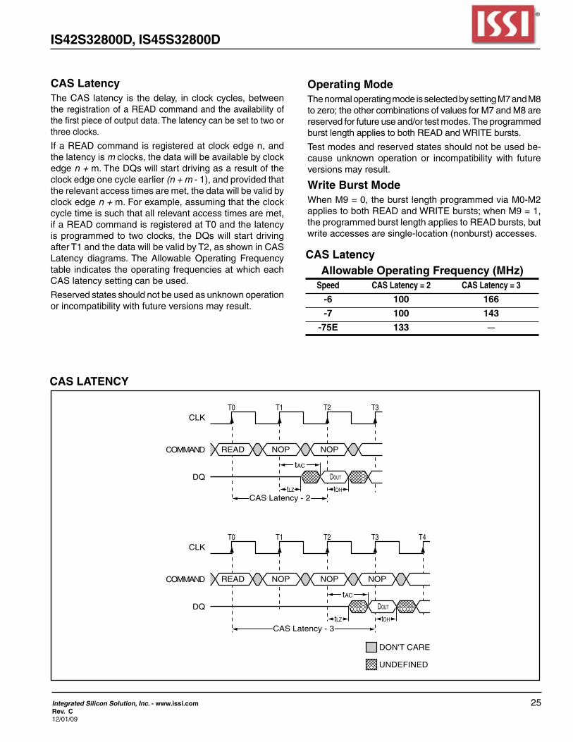
CAS LATENCY
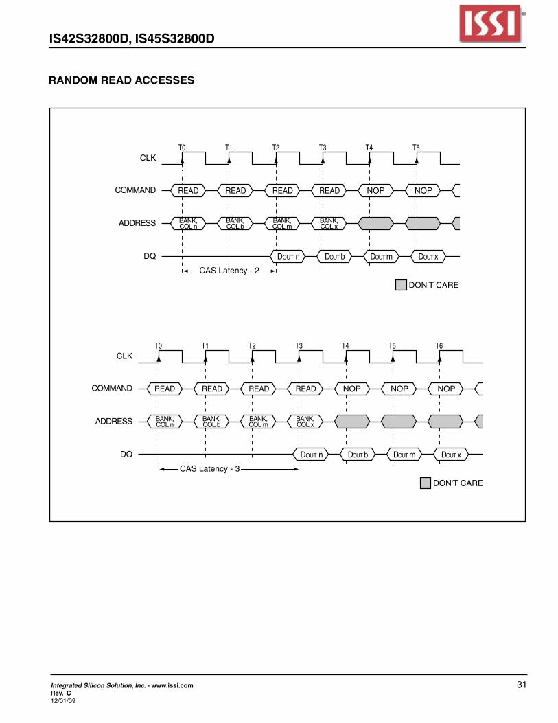
CAS LatencyTheCAS latency is thedelay, inclockcycles,betweenthe registrationofaREADcommandandtheavailabilityofthefirstpieceofoutputdata.Thelatencycanbesettotwoorthree clocks.
IfaREADcommandisregisteredatclockedgen,andthe latency is m clocks, the data will be available by clock edge n + m.TheDQswillstartdrivingasaresultoftheclock edge one cycle earlier (n + m -1),andprovidedthatthe relevant access times are met, the data will be valid by clock edge n + m.Forexample,assumingthattheclockcycle time is such that all relevant access times are met, ifaREADcommandisregisteredatT0andthelatencyisprogrammedto twoclocks, theDQswillstartdrivingafterT1andthedatawillbevalidbyT2,asshowninCASLatency diagrams.The Allowable Operating FrequencytableindicatestheoperatingfrequenciesatwhicheachCAS latency setting can be used.
Reservedstatesshouldnotbeusedasunknownoperationor incompatibility with future versions may result.
CAS LatencyAllowable Operating Frequency (MHz)
Speed CAS Latency = 2 CAS Latency = 3
-6 100 166
-7 100 143
-75E 133 —
Operating ModeThenormaloperatingmodeisselectedbysettingM7andM8tozero;theothercombinationsofvaluesforM7andM8arereservedforfutureuseand/ortestmodes.TheprogrammedburstlengthappliestobothREADandWRITEbursts.
Testmodesandreservedstatesshouldnotbeusedbe-cause unknown operation or incompatibility with future versions may result.
Write Burst ModeWhenM9=0,theburstlengthprogrammedviaM0-M2appliestobothREADandWRITEbursts;whenM9=1,theprogrammedburstlengthappliestoREADbursts,butwriteaccessesaresingle-location(nonburst)accesses.
26 Integrated Silicon Solution, Inc. - www.issi.comRev. C
12/01/09
IS42S32800D, IS45S32800D
CLK
CKE
ROW ADDRESS
BANK ADDRESS
CS
RAS
CAS
WE
A0-A11
BA0, BA1
HIGH
ACTIVATING SPECIFIC ROW WITHIN SPE-CIFIC BANK
DON'T CARE
CLK
COMMAND ACTIVE NOP NOP
tRCD
T0 T1 T2 T3 T4
READ orWRITE
CHIP OPERATION
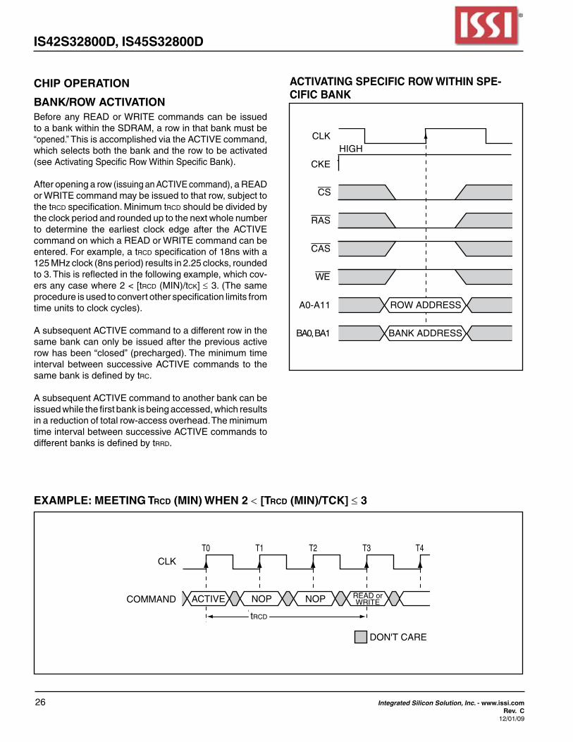
BANK/ROW ACTIVATIONBeforeanyREADorWRITEcommandscanbe issuedtoabankwithintheSDRAM,arowinthatbankmustbe“opened.”ThisisaccomplishedviatheACTIVEcommand,which selects both the bank and the row to be activated (see ActivatingSpecificRowWithinSpecificBank).
After opening a row (issuinganACTIVEcommand),aREADorWRITEcommandmaybeissuedtothatrow,subjecttothe trcdspecification.Minimumtrcd should be divided by theclockperiodandroundeduptothenextwholenumberto determine the earliest clock edge after the ACTIVEcommandonwhichaREADorWRITEcommandcanbeentered.Forexample,atrcdspecificationof18nswitha125MHzclock(8nsperiod)resultsin2.25clocks,roundedto3.Thisisreflectedinthefollowingexample,whichcov-ersanycasewhere2<[trcd(MIN)/tck] ≤3.(Thesameprocedure is used to convert other specification limits from timeunitstoclockcycles).
AsubsequentACTIVEcommandtoadifferentrowinthesame bank can only be issued after the previous active rowhasbeen“closed”(precharged).TheminimumtimeintervalbetweensuccessiveACTIVEcommands to thesame bank is defined by trc.
AsubsequentACTIVEcommandtoanotherbankcanbeissued while the first bank is being accessed, which results inareductionoftotalrow-accessoverhead.TheminimumtimeintervalbetweensuccessiveACTIVEcommandstodifferent banks is defined by trrd.
EXAMPLE: MEETING TRCD (MIN) WHEN 2 < [TRCD (MIN)/TCK] ≤ 3
IS42S32800D, IS45S32800D
Integrated Silicon Solution, Inc. - www.issi.com 27Rev. C12/01/09
CLK
CKEHIGH
COLUMN ADDRESS
AUTO PRECHARGE
NO PRECHARGE
CS
RAS
CAS
WE
A0-A8
A10
BA0, BA1 BANK ADDRESS
A9, A11
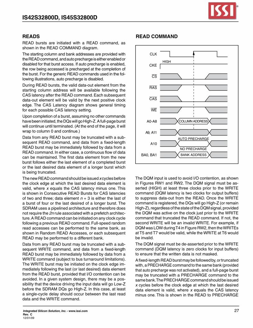
READ COMMANDREADSREAD bursts are initiated with a READ command, asshownintheREADCOMMANDdiagram.
ThestartingcolumnandbankaddressesareprovidedwiththeREADcommand,andautoprechargeiseitherenabledordisabled for that burst access. If auto precharge is enabled, the row being accessed is precharged at the completion of theburst.ForthegenericREADcommandsusedinthefol-lowing illustrations, auto precharge is disabled.
DuringREADbursts,thevaliddata-outelementfromthestarting column address will be available following the CASlatencyaftertheREADcommand.Eachsubsequentdata-outelementwillbevalidbythenextpositiveclockedge.TheCASLatencydiagramshowsgeneral timing for each possible CAS latency setting.
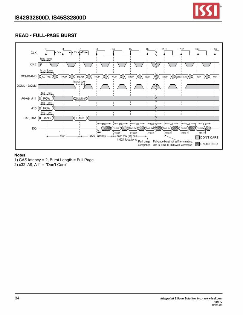
Uponcompletionofaburst,assumingnoothercommandshavebeeninitiated,theDQswillgoHigh-Z.Afull-pageburstwill continue until terminated. (At the end of the page, it will wraptocolumn0andcontinue.)
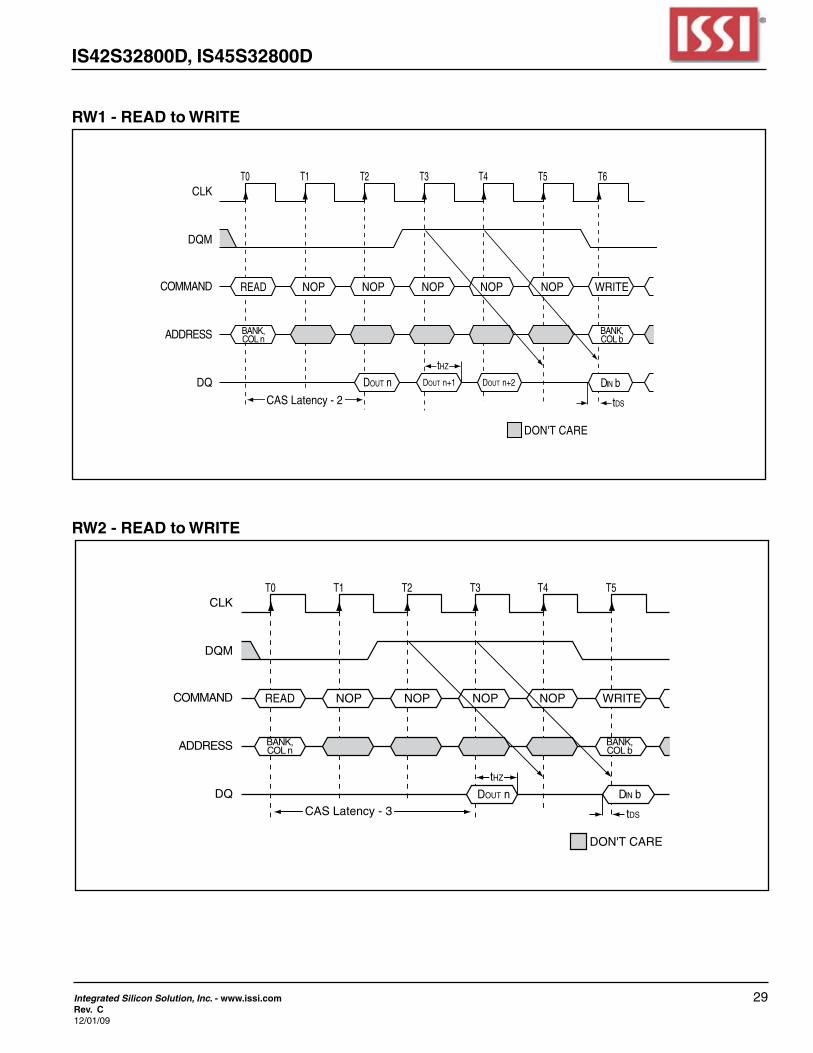
DatafromanyREADburstmaybetruncatedwithasub-sequentREADcommand,anddatafromafixed-lengthREADburstmaybeimmediatelyfollowedbydatafromaREADcommand.Ineithercase,acontinuousflowofdatacanbemaintained.Thefirstdataelementfromthenewburst follows either the last element of a completed burst or the last desired data element of a longer burst which is being truncated.
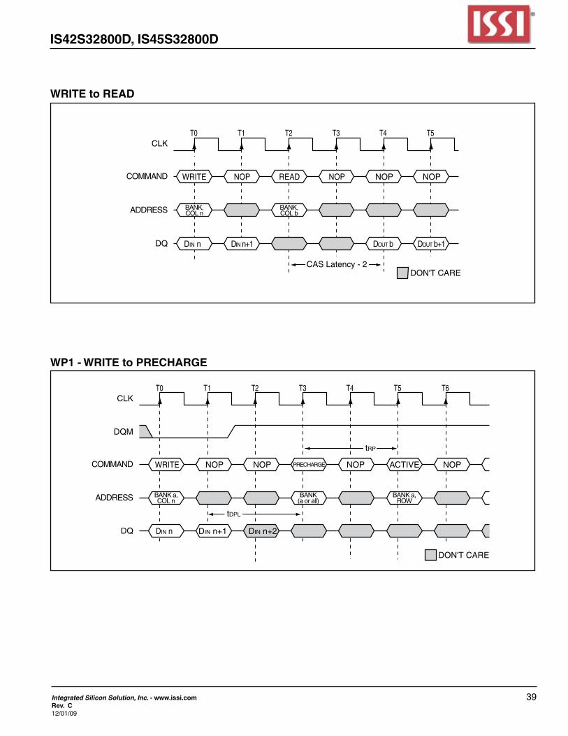
ThenewREADcommandshouldbeissuedx cycles before the clock edge at which the last desired data element is valid, where x equals theCAS latencyminusone.ThisisshowninConsecutiveREADBurstsforCASlatenciesoftwoandthree;dataelementn +3iseitherthelastofaburstoffourorthelastdesiredofalongerburst.TheSDRAMusesapipelinedarchitectureandthereforedoesnotrequirethe2n rule associated with a prefetch architec-ture.AREADcommandcanbeinitiatedonanyclockcyclefollowingapreviousREADcommand.Full-speedrandomread accesses can be performed to the same bank, as showninRandomREADAccesses,oreachsubsequentREADmaybeperformedtoadifferentbank.
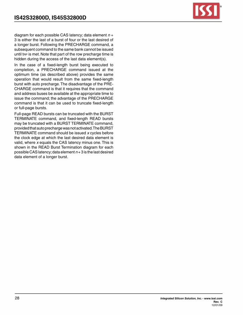
DatafromanyREADburstmaybetruncatedwithasub-sequent WRITE command, and data from a fixed-lengthREADburstmaybeimmediatelyfollowedbydatafromaWRITEcommand(subjecttobusturnaroundlimitations).TheWRITEburstmaybeinitiatedontheclockedgeim-mediatelyfollowingthelast(orlastdesired)dataelementfromtheREADburst,providedthatI/Ocontentioncanbeavoided. In a given system design, there may be a pos-sibilitythatthedevicedrivingtheinputdatawillgoLow-ZbeforetheSDRAMDQsgoHigh-Z.Inthiscase,atleasta single-cycle delay should occur between the last read dataandtheWRITEcommand.
TheDQMinputisusedtoavoidI/Ocontention,asshowninFiguresRW1andRW2.TheDQMsignalmustbeas-serted (HIGH)at least threeclocksprior to theWRITEcommand(DQMlatencyistwoclocksforoutputbuffers)tosuppressdata-out fromtheREAD.Once theWRITEcommandisregistered,theDQswillgoHigh-Z(orremainHigh-Z),regardlessofthestateoftheDQMsignal,providedtheDQMwasactiveontheclockjustpriortotheWRITEcommandthattruncatedtheREADcommand.Ifnot,thesecondWRITEwillbeaninvalidWRITE.Forexample,ifDQMwasLOWduringT4inFigureRW2,thentheWRITEsatT5andT7wouldbevalid,whiletheWRITEatT6wouldbe invalid.
TheDQMsignalmustbede-assertedpriortotheWRITEcommand(DQMlatencyiszeroclocksforinputbuffers)to ensure that the written data is not masked.
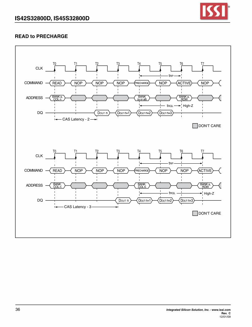
Afixed-lengthREADburstmaybefollowedby,ortruncatedwith, a PRECHARGE command to the same bank (provided thatautoprechargewasnotactivated), and a full-page burst maybetruncatedwithaPRECHARGEcommandtothesamebank.ThePRECHARGEcommandshouldbeissuedx cycles before the clock edge at which the last desired data element is valid, where x equals theCAS latencyminusone.ThisisshownintheREADtoPRECHARGE
28 Integrated Silicon Solution, Inc. - www.issi.comRev. C
12/01/09
IS42S32800D, IS45S32800D
diagramforeachpossibleCASlatency;dataelementn + 3iseitherthelastofaburstoffourorthelastdesiredofalongerburst.FollowingthePRECHARGEcommand,asubsequentcommandtothesamebankcannotbeissueduntil trpismet.Notethatpartoftherowprechargetimeishiddenduringtheaccessofthelastdataelement(s).
In the case of a fixed-length burst being executed tocompletion, a PRECHARGE command issued at theoptimum time (asdescribedabove)provides thesameoperation that would result from the same fixed-lengthburstwithautoprecharge.ThedisadvantageofthePRE-CHARGEcommandisthatitrequiresthatthecommandand address buses be available at the appropriate time to issuethecommand;theadvantageofthePRECHARGEcommandisthatitcanbeusedtotruncatefixed-lengthor full-page bursts.
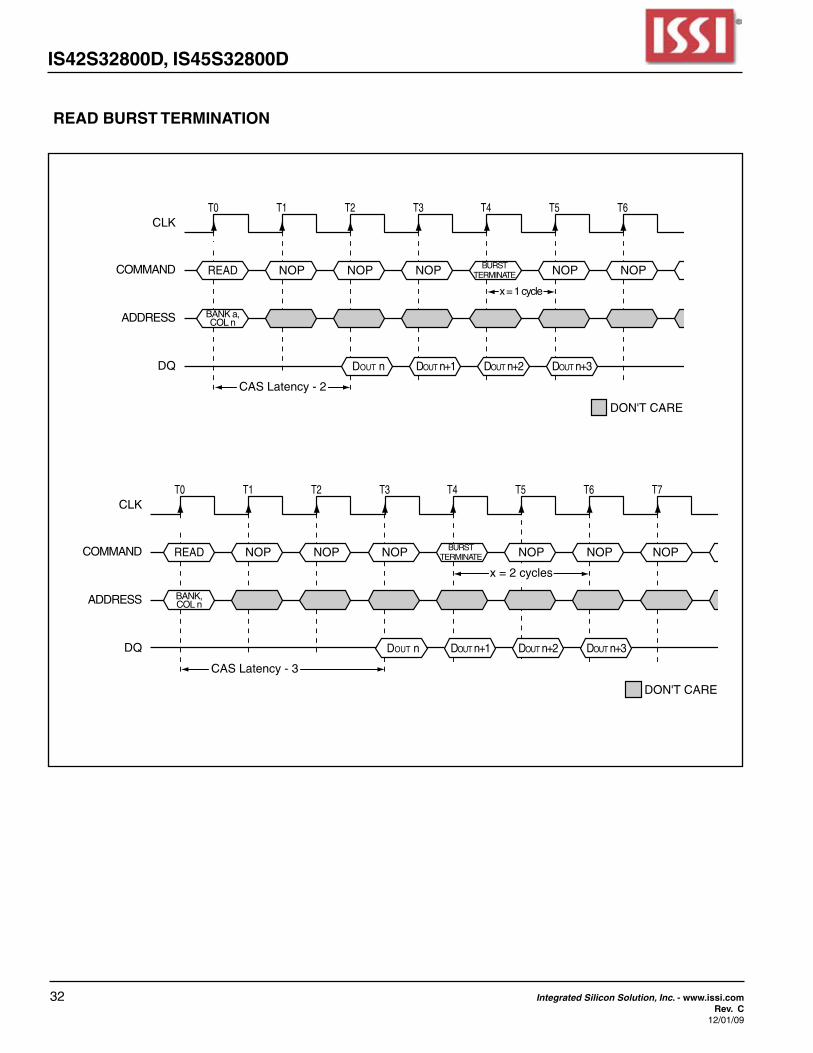
Full-pageREADburstscanbetruncatedwiththeBURSTTERMINATE command, and fixed-length READ burstsmaybetruncatedwithaBURSTTERMINATEcommand,providedthatautoprechargewasnotactivated.TheBURSTTERMINATEcommandshouldbeissuedx cycles before the clock edge at which the last desired data element is valid, where x equalstheCASlatencyminusone.ThisisshownintheREADBurstTerminationdiagramforeachpossibleCASlatency;dataelementn +3isthelastdesireddata element of a longer burst.
IS42S32800D, IS45S32800D
Integrated Silicon Solution, Inc. - www.issi.com 29Rev. C12/01/09
DON'T CARE
CLK
DQM
COMMAND
ADDRESS
DQ
T0 T1 T2 T3 T4 T5
READ NOP NOP NOP NOP WRITE
BANK,COL n
BANK,COL b
DOUT n DIN b
tDS
tHZ
CAS Latency - 3
RW1 - READ to WRITE
RW2 - READ to WRITE
DON'T CARE
CLK
DQM
COMMAND
ADDRESS
DQ
T0 T1 T2 T3 T4 T5 T6
READ NOP NOP NOP NOP NOP WRITE
BANK,COL n
DIN b
tDS
tHZ
BANK,COL b
CAS Latency - 2
DOUT n DOUT n+1 DOUT n+2
30 Integrated Silicon Solution, Inc. - www.issi.comRev. C
12/01/09
IS42S32800D, IS45S32800D
DON'T CARE
CLK
COMMAND
ADDRESS
DQ
T0 T1 T2 T3 T4 T5 T6
READ NOP NOP NOP READ NOP NOP
DOUT n DOUT n+1 DOUT n+2 DOUT n+3 DOUT b
BANK,COL n
BANK,COL b
CAS Latency - 2
DON'T CARE
CLK
COMMAND
ADDRESS
DQ
T0 T1 T2 T3 T4 T5 T6 T7
READ NOP NOP NOP READ NOP NOP NOP
DOUT n DOUT n+1 DOUT n+2 DOUT n+3 DOUT b
BANK,COL n
BANK,COL b
CAS Latency - 3
CONSECUTIVE READ BURSTS
IS42S32800D, IS45S32800D
Integrated Silicon Solution, Inc. - www.issi.com 31Rev. C12/01/09
DON'T CARE
CLK
COMMAND
ADDRESS
DQ
T0 T1 T2 T3 T4 T5
READ READ READ READ NOP NOP
DOUT n DOUT b DOUT m DOUT x
BANK,COL n
BANK,COL b
CAS Latency - 2
BANK,COL m
BANK,COL x
DON'T CARE
CLK
COMMAND
ADDRESS
DQ
T0 T1 T2 T3 T4 T5 T6
READ READ READ READ NOP NOP NOP
DOUT n DOUT b DOUT m DOUT x
BANK,COL n
BANK,COL b
CAS Latency - 3
BANK,COL m
BANK,COL x
RANDOM READ ACCESSES
32 Integrated Silicon Solution, Inc. - www.issi.comRev. C
12/01/09
IS42S32800D, IS45S32800D
DON'T CARE
CLK
COMMAND
ADDRESS
DQ
T0 T1 T2 T3 T4 T5 T6
READ NOP NOP NOP NOP NOP
DOUT n DOUT n+1 DOUT n+2 DOUT n+3
BANK a,COL n
CAS Latency - 2
x = 1 cycle
BURSTTERMINATE
DON'T CARE
CLK
COMMAND
ADDRESS
DQ
T0 T1 T2 T3 T4 T5 T6 T7
READ NOP NOP NOP NOP NOP NOP
DOUT n DOUT n+1 DOUT n+2 DOUT n+3
BANK,COL n
CAS Latency - 3
x = 2 cycles
BURSTTERMINATE
READ BURST TERMINATION
IS42S32800D, IS45S32800D
Integrated Silicon Solution, Inc. - www.issi.com 33Rev. C12/01/09
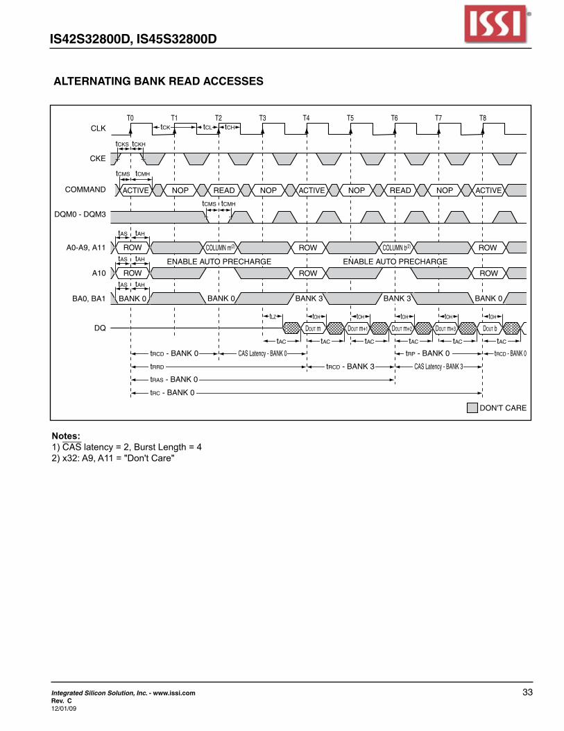
ALTERNATING BANK READ ACCESSES
Notes:1) CAS latency = 2, Burst Length = 42) x32: A9, A11 = "Don't Care"
BANK 0 BANK 3 BANK 3 BANK 0
DON'T CARE
CLK
CKE
COMMAND
DQM0 - DQM3
A0-A9, A11
A10
BA0, BA1
DQ
tCMS tCMH
tAS tAH
tAS tAH
tAS tAH
tRCD - BANK 0 CAS Latency - BANK 0 tRCD - BANK 0
tRAS - BANK 0
tRC - BANK 0
tCHtCLtCK
tCMS tCMH
tCKS tCKH
ACTIVE NOP READ NOP ACTIVE NOP READ NOP ACTIVE
ROW
ROW
BANK 0
ROW ROW
tRRD tRCD - BANK 3
tRP - BANK 0
COLUMN m(2) ROW COLUMN b(2) ROW
ENABLE AUTO PRECHARGE ENABLE AUTO PRECHARGE
T0 T1 T2 T3 T4 T5 T6 T7 T8
tAC
tOH tOH tOH tOH tOH
DOUT m DOUT m+1 DOUT m+2 DOUT m+3 DOUT b
tAC tAC tAC tAC tAC
tLZ
CAS Latency - BANK 3
34 Integrated Silicon Solution, Inc. - www.issi.comRev. C
12/01/09
IS42S32800D, IS45S32800D
READ - FULL-PAGE BURST
Notes:1) CAS latency = 2, Burst Length = Full Page2) x32: A9, A11 = "Don't Care"
DON'T CARE
UNDEFINED
CLK
CKE
COMMAND
DQM0 - DQM3
A0-A9, A11
A10
BA0, BA1
DQ
tCMS tCMH
ACTIVE NOP READ NOP NOP NOP NOP NOP BURST TERM NOP NOP
tAS tAH
tAS tAH
tAS tAH
ROW
ROW
BANK
COLUMN m(2)
tCHtCLtCK
tCMS tCMH
tCKS tCKH
BANK
tRCD CAS Latency
tAC tACtAC tACtAC tHZ
tLZ
tAC
tOH tOH tOH tOH tOH tOH
DOUT m DOUT m+1 DOUT m+2 DOUT m-1 DOUT m DOUT m+1
each row (x4) has1,024 locations
Full pagecompletion
Full-page burst not self-terminating.Use BURST TERMINATE command.
T0 T1 T2 T3 T4 T5 T6 Tn+1 Tn+2 Tn+3 Tn+4
IS42S32800D, IS45S32800D
Integrated Silicon Solution, Inc. - www.issi.com 35Rev. C12/01/09
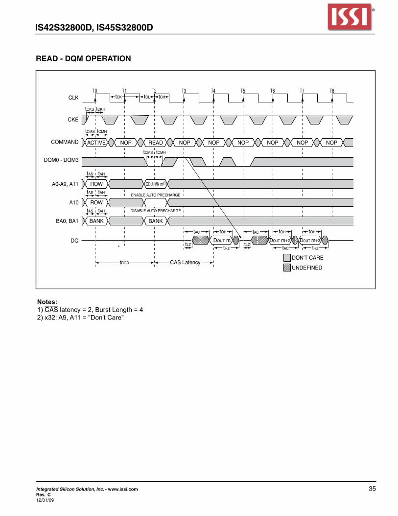
READ - DQM OPERATION
DON'T CARE
UNDEFINED
CLK
CKE
COMMAND
DQM0 - DQM3
A0-A9, A11
A10
BA0, BA1
DQ
tCMS tCMH
ACTIVE NOP READ NOP NOP NOP NOP NOP NOP
tAS tAH
tAS tAH
tAS tAH
ENABLE AUTO PRECHARGE
DISABLE AUTO PRECHARGE
ROW
ROW
BANK
tRCD CAS Latency
DOUT m DOUT m+2 DOUT m+3
COLUMN m(2)
BANK
tCHtCLtCK
tCMS tCMH
tCKS tCKH
tOHtOHtOH tACtAC
tACtHZ tHZtLZ tLZ
T0 T1 T2 T3 T4 T5 T6 T7 T8
Notes:1) CAS latency = 2, Burst Length = 42) x32: A9, A11 = "Don't Care"
36 Integrated Silicon Solution, Inc. - www.issi.comRev. C
12/01/09
IS42S32800D, IS45S32800D
DON'T CARE
CLK
COMMAND
ADDRESS
DQ
T0 T1 T2 T3 T4 T5 T6 T7
READ NOP NOP NOP NOP ACTIVE NOP
DOUT n DOUT n+1 DOUT n+2 DOUT n+3
BANK a,COL n
BANK a,ROW
BANK(a or all)
CAS Latency - 2
tRP
PRECHARGE
tRQL High-Z
DON'T CARE
CLK
COMMAND
ADDRESS
DQ
T0 T1 T2 T3 T4 T5 T6 T7
READ NOP NOP NOP NOP NOP ACTIVE
DOUT n DOUT n+1 DOUT n+2 DOUT n+3
BANK,COL n
BANK,COL b
CAS Latency - 3
tRP
tRQL
BANK a,ROW
PRECHARGE
High-Z
READ to PRECHARGE
IS42S32800D, IS45S32800D
Integrated Silicon Solution, Inc. - www.issi.com 37Rev. C12/01/09
CLK
CKEHIGH
COLUMN ADDRESS
AUTO PRECHARGE
BANK ADDRESS
CS
RAS
CAS
WE
A0-A8
A10
BA0, BA1
NO PRECHARGE
A9, A11
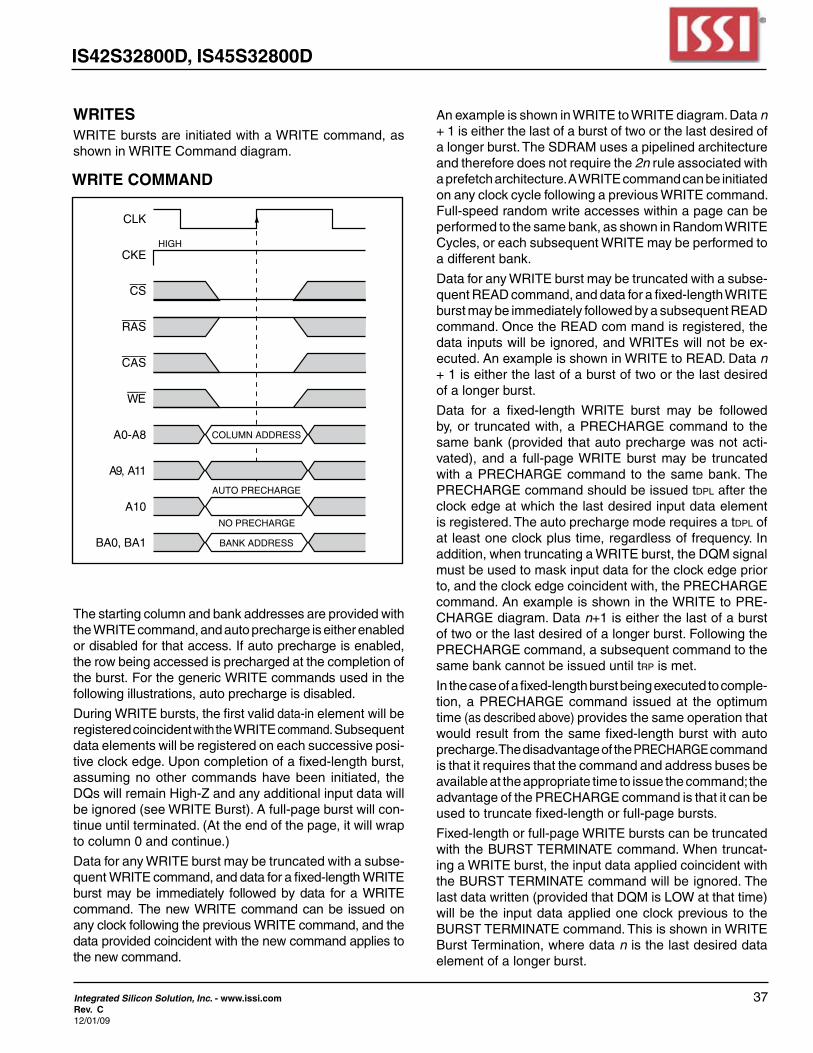
WRITE COMMAND
ThestartingcolumnandbankaddressesareprovidedwiththeWRITEcommand,andautoprechargeiseitherenabledor disabled for that access. If auto precharge is enabled, the row being accessed is precharged at the completion of theburst.ForthegenericWRITEcommandsusedinthefollowing illustrations, auto precharge is disabled.
DuringWRITEbursts,thefirstvaliddata-in element will be registered coincident with the WRITEcommand.Subsequentdata elements will be registered on each successive posi-tiveclockedge.Uponcompletionofafixed-lengthburst,assuming no other commands have been initiated, the DQswillremainHigh-Zandanyadditionalinputdatawillbeignored(seeWRITEBurst).Afull-pageburstwillcon-tinue until terminated. (At the end of the page, it will wrap tocolumn0andcontinue.)
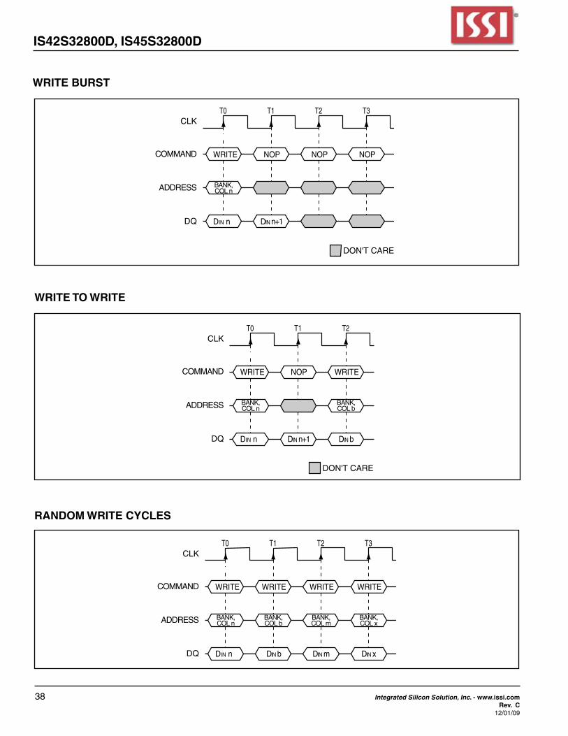
DataforanyWRITEburstmaybetruncatedwithasubse-quentWRITEcommand,anddataforafixed-lengthWRITEburstmaybe immediately followedbydata foraWRITEcommand.ThenewWRITEcommandcanbe issuedonanyclockfollowingthepreviousWRITEcommand,andthedata provided coincident with the new command applies to the new command.
AnexampleisshowninWRITEtoWRITEdiagram.Datan + 1 is either the last of a burst of two or the last desired of alongerburst.TheSDRAMusesapipelinedarchitectureandthereforedoesnotrequirethe2n rule associated with aprefetcharchitecture.AWRITEcommandcanbeinitiatedonanyclockcyclefollowingapreviousWRITEcommand.Full-speedrandomwriteaccesseswithinapagecanbeperformedtothesamebank,asshowninRandomWRITECycles,oreachsubsequentWRITEmaybeperformedtoa different bank.
DataforanyWRITEburstmaybetruncatedwithasubse-quentREADcommand,anddataforafixed-lengthWRITEburstmaybeimmediatelyfollowedbyasubsequentREADcommand.OncetheREADcommandisregistered,thedatainputswillbeignored,andWRITEswillnotbeex-ecuted.AnexampleisshowninWRITEtoREAD.Datan + 1 is either the last of a burst of two or the last desired of a longer burst.
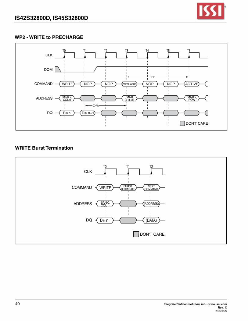
Data for a fixed-length WRITE burst may be followedby,or truncatedwith,aPRECHARGEcommandto thesame bank (provided that auto precharge was not acti-vated), anda full-pageWRITEburstmaybe truncatedwithaPRECHARGEcommand to thesamebank.ThePRECHARGEcommandshouldbeissuedtdpl after the clock edge at which the last desired input data element isregistered.Theautoprechargemoderequiresatdpl of atleastoneclockplustime,regardlessoffrequency.Inaddition,whentruncatingaWRITEburst,theDQMsignalmust be used to mask input data for the clock edge prior to,andtheclockedgecoincidentwith,thePRECHARGEcommand.AnexampleisshownintheWRITEtoPRE-CHARGEdiagram.Datan+1 is either the last of a burst oftwoorthelastdesiredofalongerburst.FollowingthePRECHARGEcommand,asubsequentcommandtothesame bank cannot be issued until trp is met.
Inthecaseofafixed-lengthburstbeingexecutedtocomple-tion,aPRECHARGEcommand issuedat theoptimumtime (asdescribedabove) provides the same operation that wouldresult fromthesamefixed-lengthburstwithautoprecharge.ThedisadvantageofthePRECHARGE command isthatitrequiresthatthecommandandaddressbusesbeavailableattheappropriatetimetoissuethecommand;theadvantageofthePRECHARGEcommandisthatitcanbeusedtotruncatefixed-lengthorfull-pagebursts.
Fixed-lengthorfull-pageWRITEburstscanbetruncatedwiththeBURSTTERMINATEcommand.Whentruncat-ingaWRITEburst,theinputdataappliedcoincidentwiththeBURSTTERMINATEcommandwillbeignored.Thelastdatawritten(providedthatDQMisLOWatthattime)will be the input data applied one clock previous to the BURSTTERMINATEcommand.ThisisshowninWRITEBurstTermination,wheredatan is the last desired data element of a longer burst.
WRITESWRITEburstsareinitiatedwithaWRITEcommand,asshowninWRITECommanddiagram.
38 Integrated Silicon Solution, Inc. - www.issi.comRev. C
12/01/09
IS42S32800D, IS45S32800D
CLK
COMMAND
ADDRESS
DQ
T0 T1 T2 T3
WRITE NOP NOP NOP
DIN n DIN n+1
BANK,COL n
DON'T CARE
CLK
COMMAND
ADDRESS
DQ
T0 T1 T2
WRITE NOP WRITE
DIN n DIN n+1 DIN b
BANK,COL n
BANK,COL b
DON'T CARE
WRITE BURST
WRITE TO WRITE
CLK
COMMAND
ADDRESS
DQ
T0 T1 T2 T3
WRITE WRITE WRITE WRITE
DIN n DIN b DIN m DIN x
BANK,COL n
BANK,COL b
BANK,COL m
BANK,COL x
RANDOM WRITE CYCLES
IS42S32800D, IS45S32800D
Integrated Silicon Solution, Inc. - www.issi.com 39Rev. C12/01/09
DON'T CARE
CLK
COMMAND
ADDRESS
DQ
T0 T1 T2 T3 T4 T5
WRITE NOP READ NOP NOP NOP
DIN n DIN n+1 DOUT b DOUT b+1
BANK,COL n
BANK,COL b
CAS Latency - 2
WRITE to READ
WP1 - WRITE to PRECHARGE
DON'T CARE
CLK
DQM
COMMAND
ADDRESS
DQ
T0 T1 T2 T3 T4 T5 T6
WRITE NOP NOP NOP ACTIVE NOP
BANK a,COL n
BANK a,ROW
BANK(a or all)
tDPL
tRP
PRECHARGE
DIN n DIN n+1 DIN n+2
40 Integrated Silicon Solution, Inc. - www.issi.comRev. C
12/01/09
IS42S32800D, IS45S32800D
CLK
COMMAND
ADDRESS
DQ
T0 T1 T2
WRITE
DIN n (DATA)
BANK,COL n
DON'T CARE
(ADDRESS)
BURSTTERMINATE
NEXTCOMMAND
WRITE Burst Termination
DON'T CARE
CLK
DQM
COMMAND
ADDRESS
DQ
T0 T1 T2 T3 T4 T5 T6
WRITE NOP NOP NOP NOP ACTIVE
BANK a,COL n
BANK a,ROW
BANK(a or all)
tDPL
tRP
PRECHARGE
DIN n DIN n+1
WP2 - WRITE to PRECHARGE
IS42S32800D, IS45S32800D
Integrated Silicon Solution, Inc. - www.issi.com 41Rev. C12/01/09
DON'T CARE
CLK
CKE
COMMAND
DQM0 - DQM3
A0-A9, A11
A10
BA0, BA1
DQ
tCMS tCMH
ACTIVE NOP WRITE NOP NOP NOP NOP BURST TERM NOP
tAS tAH
tAS tAH
tAS tAH
tDS tDH tDS tDH tDS tDH
ROW
ROW
BANK
tRCD
DIN m DIN m+1 DIN m+2 DIN m+3 DIN m-1
COLUMN m(2)
tCHtCLtCK
tDS tDH tDS tDH tDS tDH
tCMS tCMH
tCKS tCKH
BANK
Full page completed
T0 T1 T2 T3 T4 T5 Tn+1 Tn+2
WRITE - FULL PAGE BURST
Notes:1) Burst Length = Full Page2) x32: A9, A11 = "Don't Care"
42 Integrated Silicon Solution, Inc. - www.issi.comRev. C
12/01/09
IS42S32800D, IS45S32800D
DON'T CARE
CLK
CKE
COMMAND
DQM0 - DQM3
A0-A9, A11
A10
BA0, BA1
DQ
tCMS tCMH
ACTIVE NOP WRITE NOP NOP NOP NOP NOP
tAS tAH
tAS tAH
tAS tAH
tDS tDH tDS tDH tDS tDH
ENABLE AUTO PRECHARGE
DISABLE AUTO PRECHARGE
ROW
ROW
BANK
tRCD
DIN m DIN m+2 DIN m+3
COLUMN m(2)
BANK
tCHtCLtCK
tCMS tCMH
tCKS tCKH
T0 T1 T2 T3 T4 T5 T6 T7
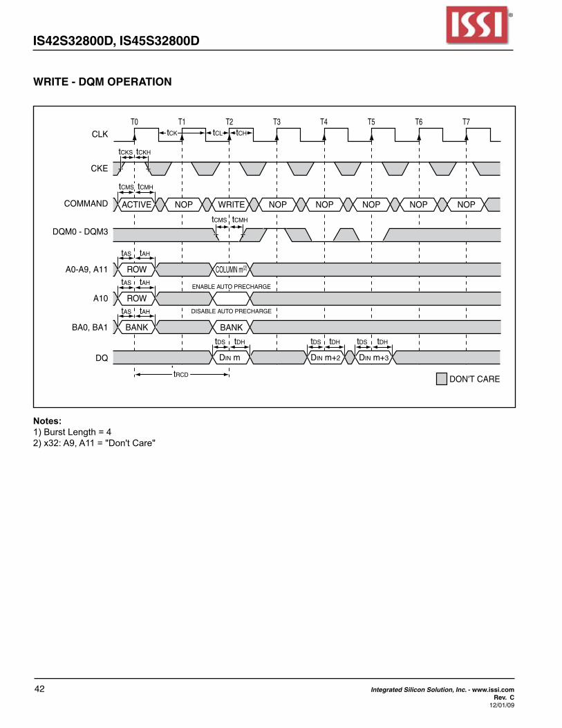
WRITE - DQM OPERATION
Notes:1) Burst Length = 42) x32: A9, A11 = "Don't Care"
IS42S32800D, IS45S32800D
Integrated Silicon Solution, Inc. - www.issi.com 43Rev. C12/01/09
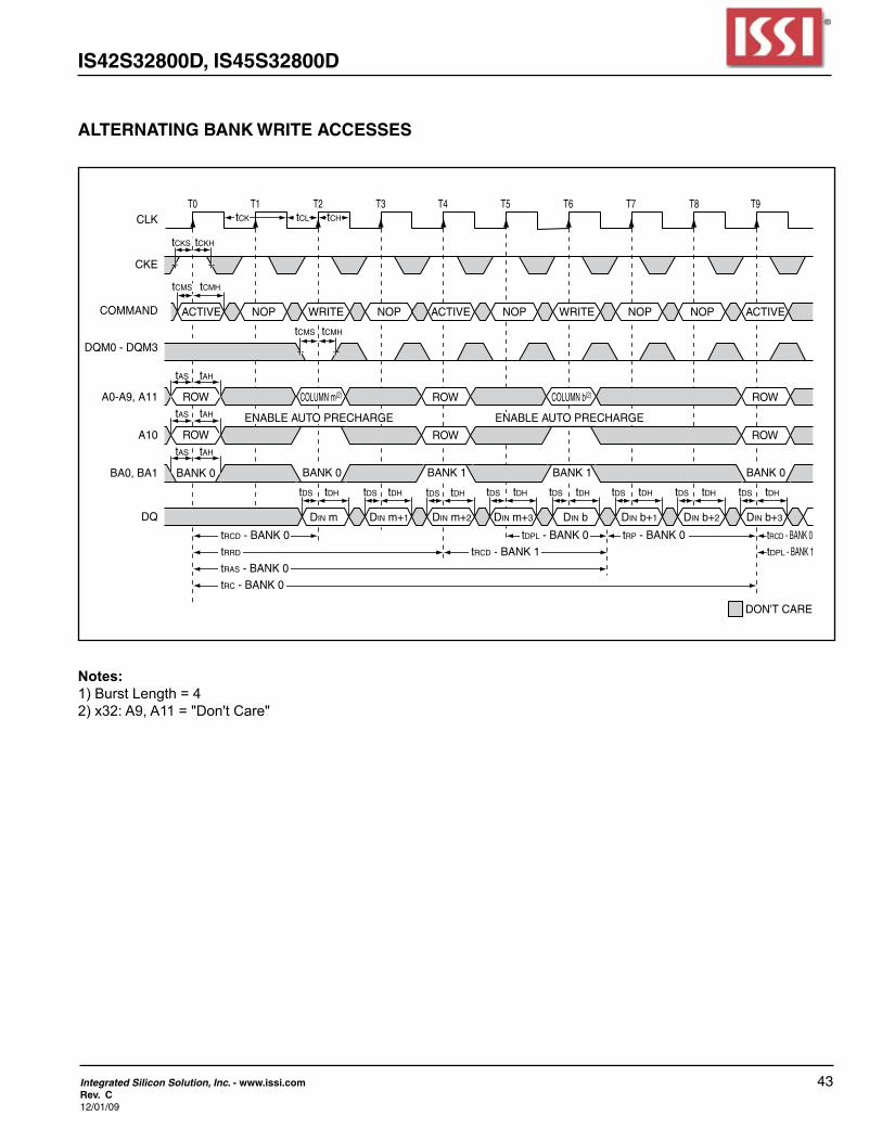
ALTERNATING BANK WRITE ACCESSES
BANK 0 BANK 1 BANK 1 BANK 0
DON'T CARE
CLK
CKE
COMMAND
DQM0 - DQM3
A0-A9, A11
A10
BA0, BA1
DQ
tCMS tCMH
tAS tAH
tAS tAH
tAS tAH
tDS tDH tDS tDH tDS tDH
tRCD - BANK 0 tRCD - BANK 0tDPL - BANK 1
tRAS - BANK 0tRC - BANK 0
tCHtCLtCK
tDS tDH tDS tDH tDS tDH tDS tDH tDS tDH
tCMS tCMH
tCKS tCKH
ACTIVE NOP WRITE NOP ACTIVE NOP WRITE NOP NOP ACTIVE
DIN m DIN m+1 DIN m+2 DIN m+3 DIN b DIN b+1 DIN b+2 DIN b+3
ROW
ROW
BANK 0
ROW ROW
tRRD tRCD - BANK 1
tDPL - BANK 0 tRP - BANK 0
COLUMN m(2) ROW COLUMN b(2) ROW
ENABLE AUTO PRECHARGE ENABLE AUTO PRECHARGE
T0 T1 T2 T3 T4 T5 T6 T7 T8 T9
Notes:1) Burst Length = 42) x32: A9, A11 = "Don't Care"
44 Integrated Silicon Solution, Inc. - www.issi.comRev. C
12/01/09
IS42S32800D, IS45S32800D
DON'T CARE
CLK
CKE
COMMAND
ADDRESS
DQ
T0 T1 T2 T3 T4 T5
NOP WRITE NOP NOP
BANK a,COL n
DIN n DIN n+1 DIN n+2
INTERNALCLOCK
DON'T CARE
CLK
CKE
COMMAND
ADDRESS
DQ
T0 T1 T2 T3 T4 T5 T6
READ NOP NOP NOP NOP NOP
BANK a,COL n
DOUT n DOUT n+1 DOUT n+2 DOUT n+3
INTERNALCLOCK
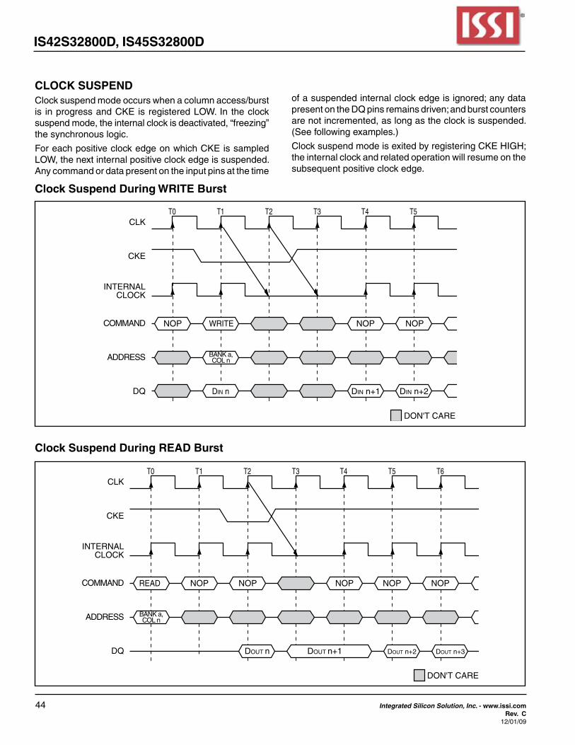
CLOCK SUSPENDClock suspend mode occurs when a column access/burst is inprogressandCKEisregisteredLOW.In theclocksuspendmode,theinternalclockisdeactivated,“freezing”the synchronous logic.
ForeachpositiveclockedgeonwhichCKEissampledLOW,thenextinternalpositiveclockedgeissuspended.Any command or data present on the input pins at the time
ofasuspendedinternalclockedgeisignored;anydatapresentontheDQpinsremainsdriven;andburstcountersare not incremented, as long as the clock is suspended. (Seefollowingexamples.)
ClocksuspendmodeisexitedbyregisteringCKEHIGH;the internal clock and related operation will resume on the subsequentpositiveclockedge.
Clock Suspend During WRITE Burst
Clock Suspend During READ Burst
IS42S32800D, IS45S32800D
Integrated Silicon Solution, Inc. - www.issi.com 45Rev. C12/01/09
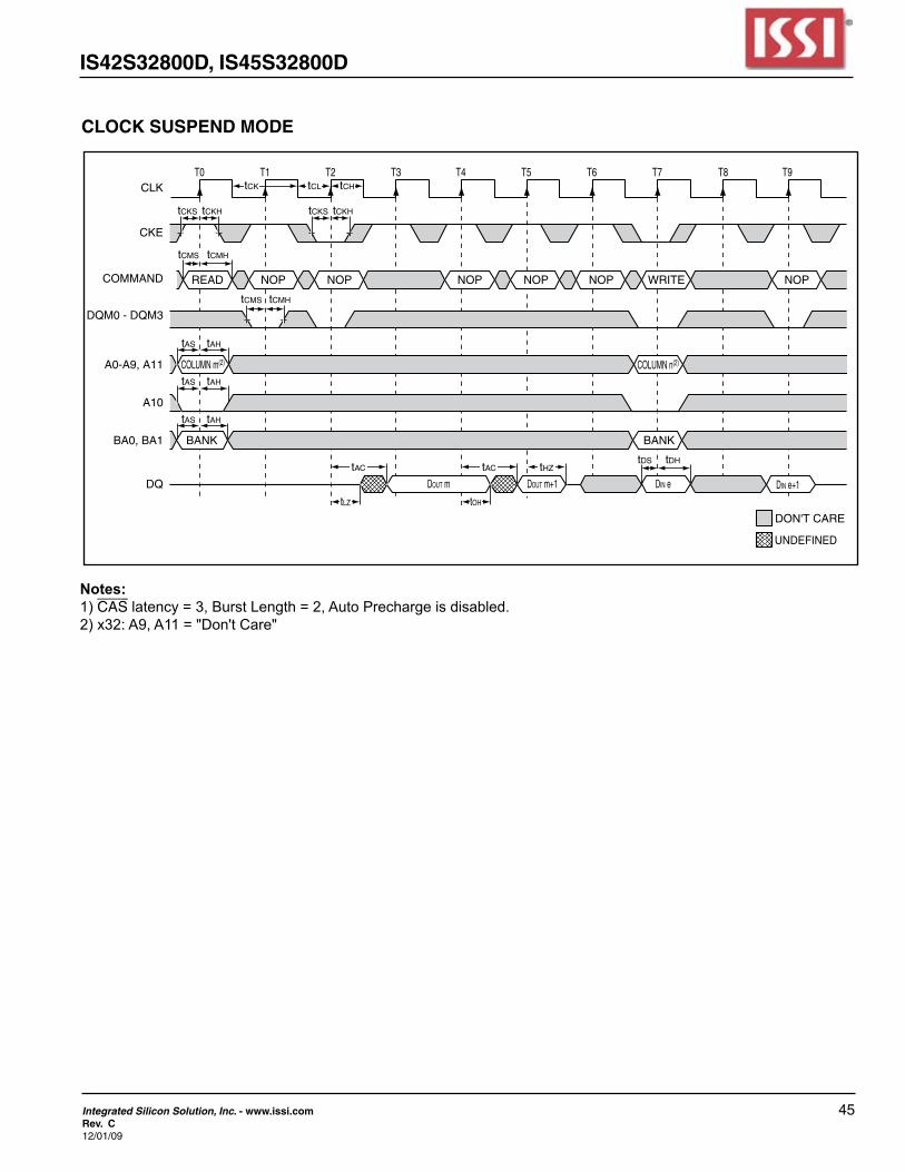
CLOCK SUSPEND MODE
Notes:1) CAS latency = 3, Burst Length = 2, Auto Precharge is disabled.2) x32: A9, A11 = "Don't Care"
DON'T CARE
CLK
CKE
COMMAND
DQM0 - DQM3
A0-A9, A11
A10
BA0, BA1
DQ
tCMS tCMH
tAS tAH
tAS tAH
tAS tAH
tCHtCLtCK
tCMS tCMH
tCKS tCKH
COLUMN m(2)
T0 T1 T2 T3 T4 T5 T6 T7 T8 T9
READ NOP NOP NOP NOP NOP WRITE NOP
tCKS tCKH
BANK BANK
COLUMN n(2)
tAC tAC
tOH
tHZ
DOUT m DOUT m+1
tLZ
UNDEFINED
DIN e+1
tDS tDH
DIN e
46 Integrated Silicon Solution, Inc. - www.issi.comRev. C
12/01/09
IS42S32800D, IS45S32800D
CLK
CKEHIGH
ALL BANKS
BANK SELECT
BANK ADDRESS
CS
RAS
CAS
WE
A0-A9, A11
A10
BA0, BA1
DON'T CARE
CLK
CKE
COMMAND NOP NOP ACTIVE
≥ tCKStCKS
All banks idle
Enter power-down mode Exit power-down mode
tRCD
tRAS
tRC
Input buffers gated off
less than TREF
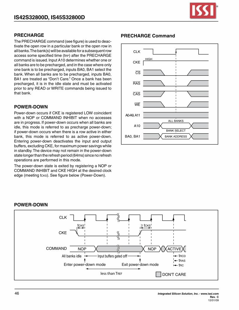
PRECHARGE Command
POWER-DOWN
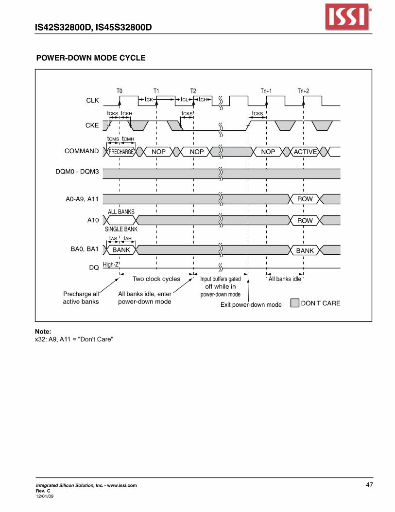
POWER-DOWNPower-downoccursifCKEisregisteredLOWcoincidentwithaNOPorCOMMANDINHIBITwhennoaccessesare in progress. If power-down occurs when all banks are idle,thismodeisreferredtoasprechargepower-down;if power-down occurs when there is a row active in either bank, this mode is referred to as active power-down. Entering power-down deactivates the input and output buffers,excludingCKE,formaximumpowersavingswhileinstandby.Thedevicemaynotremaininthepower-downstatelongerthantherefreshperiod(64ms)sincenorefreshoperations are performed in this mode.
Thepower-downstateisexitedbyregisteringaNOPorCOMMANDINHIBITandCKEHIGHatthedesiredclockedge (meeting tcks).Seefigurebelow(Power-Down).
PRECHARGEThePRECHARGEcommand(seefigure)isusedtodeac-tivate the open row in a particular bank or the open row in allbanks.Thebank(s)willbeavailableforasubsequentrowaccess some specified time (trp)afterthePRECHARGEcommand is issued. Input A10 determines whether one or all banks are to be precharged, and in the case where only onebankistobeprecharged,inputsBA0,BA1selectthebank.Whenallbanksaretobeprecharged,inputsBA0,BA1aretreatedas“Don’tCare.”Onceabankhasbeenprecharged, it is in the idle state and must be activated priortoanyREADorWRITEcommandsbeingissuedtothat bank.
IS42S32800D, IS45S32800D
Integrated Silicon Solution, Inc. - www.issi.com 47Rev. C12/01/09
POWER-DOWN MODE CYCLE
DON'T CARE
CLK
CKE
COMMAND
DQM0 - DQM3
A0-A9, A11
A10
BA0, BA1
DQ
tAS tAH
BANK
tCHtCLtCK
tCMS tCMH
tCKS tCKH
PRECHARGE NOP NOP NOP ACTIVE
ALL BANKS
SINGLE BANK
ROW
ROW
BANK
tCKStCKS
Precharge allactive banks
All banks idleTwo clock cycles Input buffers gatedoff while in
power-down modeAll banks idle, enterpower-down mode Exit power-down mode
T0 T1 T2 Tn+1 Tn+2
High-Z
Note:x32: A9, A11 = "Don't Care"
48 Integrated Silicon Solution, Inc. - www.issi.comRev. C
12/01/09
IS42S32800D, IS45S32800D
DON'T CARE
CLK
COMMAND
BANK n
BANK m
ADDRESS
DQ
T0 T1 T2 T3 T4 T5 T6 T7
NOP NOP NOP NOP NOP NOP
DOUT a DOUT a+1 DOUT b DOUT b+1
BANK n,COL a
CAS Latency - 3 (BANK n)
CAS Latency - 3 (BANK m)
tRP - BANK n tRP - BANK m
READ - APBANK n
READ - APBANK m
Page Active READ with Burst of 4 Interrupt Burst, Precharge Idle
Page Active READ with Burst of 4 Precharge
Internal States
BANK n,COL b
DON'T CARE
CLK
COMMAND
BANK n
BANK m
ADDRESS
DQM
DQ
T0 T1 T2 T3 T4 T5 T6 T7
NOP NOP NOP NOP NOP NOP
DOUT a DIN b DIN b+1 DIN b+2 DIN b+3
BANK n,COL a
BANK m,COL b
CAS Latency - 3 (BANK n)
tRP - BANK n tDPL - BANK m
READ - APBANK n
WRITE - APBANK m
READ with Burst of 4 Interrupt Burst, Precharge Idle
Page Active WRITE with Burst of 4 Write-Back
Internal States Page Active
BURST READ/SINGLE WRITETheburstread/singlewritemodeisenteredbyprogrammingthe write burst mode bit (M9) in the mode register to a logic 1. In this mode, all WRITE commands result in the access ofasinglecolumnlocation(burstofone),regardlessoftheprogrammedburstlength.READcommandsaccess columns according to the programmed burst length and sequence,justasinthenormalmodeofoperation(M9=0).
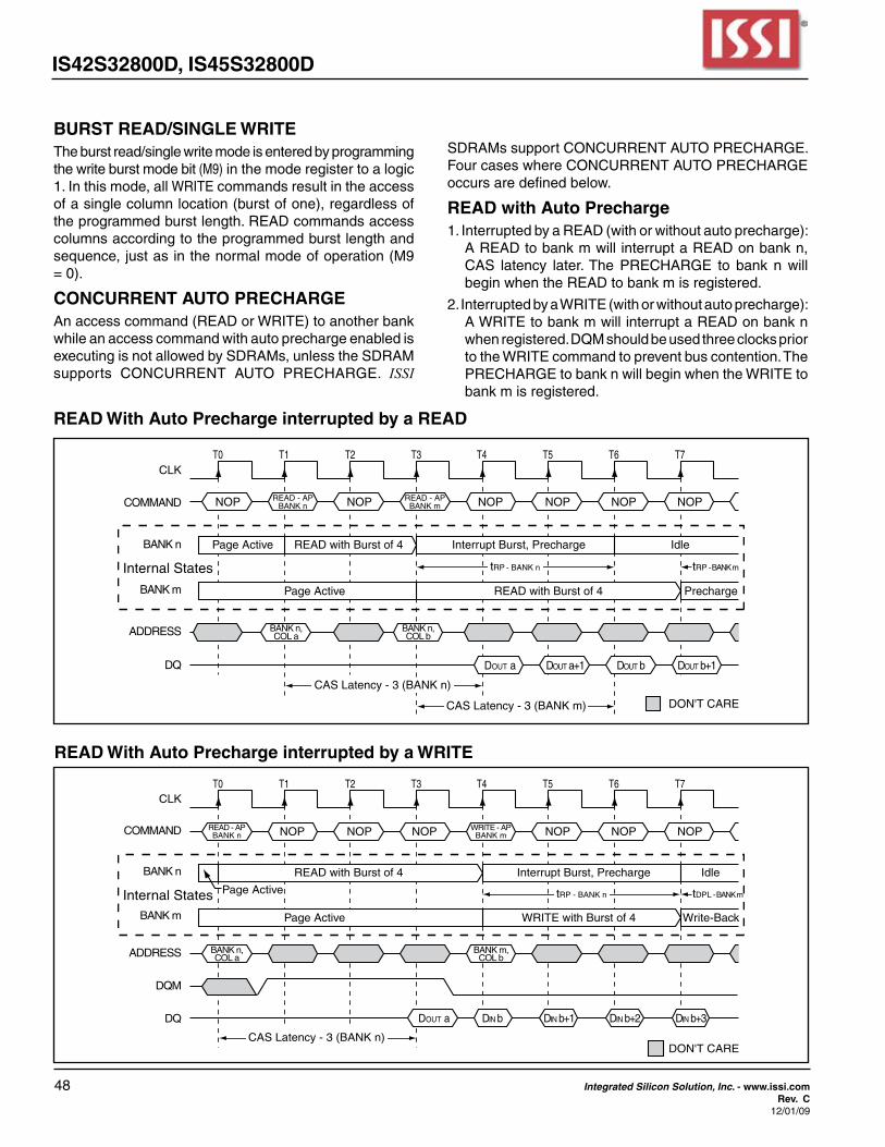
CONCURRENT AUTO PRECHARGEAnaccesscommand(READorWRITE)toanotherbankwhile an access command with auto precharge enabled is executingisnotallowedbySDRAMs,unlesstheSDRAMsupports CONCURRENT AUTO PRECHARGE. ISSI
SDRAMssupportCONCURRENTAUTOPRECHARGE.FourcaseswhereCONCURRENTAUTOPRECHARGEoccurs are defined below.
READ with Auto Precharge1.InterruptedbyaREAD(withorwithoutautoprecharge):
AREADtobankmwill interruptaREADonbankn,CAS latency later.The PRECHARGE to bank n willbeginwhentheREADtobankmisregistered.
2.InterruptedbyaWRITE(withorwithoutautoprecharge):AWRITEtobankmwillinterruptaREADonbanknwhenregistered.DQMshouldbeusedthreeclockspriortotheWRITEcommandtopreventbuscontention.ThePRECHARGEtobanknwillbeginwhentheWRITEtobank m is registered.
READ With Auto Precharge interrupted by a READ
READ With Auto Precharge interrupted by a WRITE
IS42S32800D, IS45S32800D
Integrated Silicon Solution, Inc. - www.issi.com 49Rev. C12/01/09
DON'T CARE
CLK
COMMAND
BANK n
BANK m
ADDRESS
DQ
T0 T1 T2 T3 T4 T5 T6 T7
NOP NOP NOP NOP NOP NOP
DIN a DIN a+1 DOUT b DOUT b+1
BANK n,COL a
BANK m,COL b
CAS Latency - 3 (BANK m)
tRP - BANK ntRP - BANK m
WRITE - APBANK n
READ - APBANK m
Page Active WRITE with Burst of 4 Interrupt Burst, Write-Back Precharge
Page Active READ with Burst of 4 Precharge
Internal States tDPL - BANK n
DON'T CARE
CLK
COMMAND
BANK n
BANK m
ADDRESS
DQ
T0 T1 T2 T3 T4 T5 T6 T7
NOP NOP NOP NOP NOP NOP
BANK n,COL a
BANK m,COL b
tRP - BANK ntDPL - BANK m
WRITE - APBANK n
WRITE - APBANK m
Page Active WRITE with Burst of 4 Interrupt Burst, Write-Back Precharge
Page Active WRITE with Burst of 4 Write-Back
Internal States tDPL - BANK n
DIN a DIN a+1 DIN a+2 DIN b DIN b+1 DIN b+2 DIN b+3
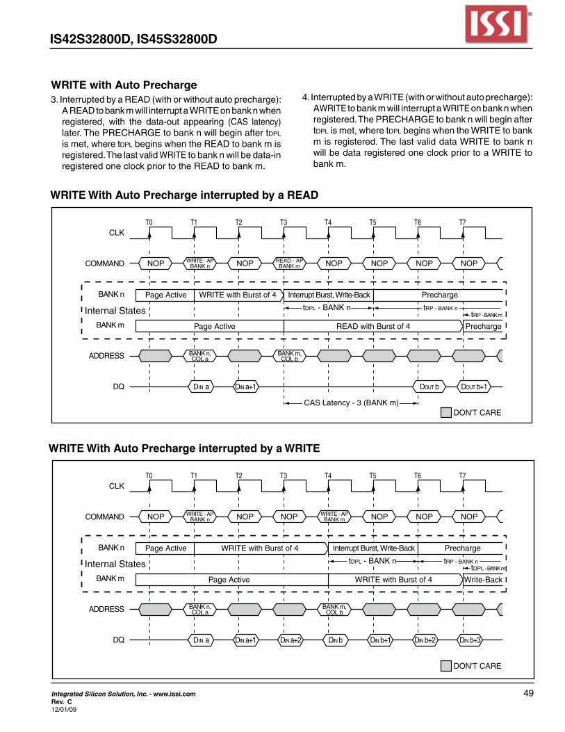
WRITE with Auto Precharge3.InterruptedbyaREAD(withorwithoutautoprecharge):
AREADtobankmwillinterruptaWRITEonbanknwhenregistered, with the data-out appearing (CAS latency) later.ThePRECHARGEtobanknwillbeginaftertdpl is met, where tdplbeginswhentheREADtobankmisregistered.ThelastvalidWRITE to bank n will be data-in registeredoneclockpriortotheREADtobankm.
4.InterruptedbyaWRITE(withorwithoutautoprecharge):AWRITE to bank m will interrupt a WRITE on bank n when registered.ThePRECHARGEtobanknwillbeginaftertdpl is met, where tdplbeginswhentheWRITEtobankmisregistered.ThelastvaliddataWRITEtobanknwillbedataregisteredoneclockpriortoaWRITEtobank m.
WRITE With Auto Precharge interrupted by a READ
WRITE With Auto Precharge interrupted by a WRITE
50 Integrated Silicon Solution, Inc. - www.issi.comRev. C
12/01/09
IS42S32800D, IS45S32800D
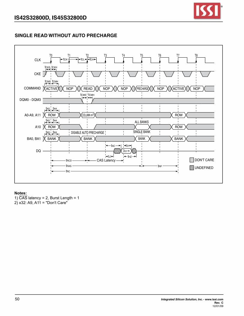
SINGLE READ WITHOUT AUTO PRECHARGE
DON'T CARE
UNDEFINED
CLK
CKE
COMMAND
DQM0 - DQM3
A0-A9, A11
A10
BA0, BA1
DQ
tCMS tCMH
ACTIVE NOP READ NOP NOP PRECHARGE NOP ACTIVE NOP
tAS tAH
tAS tAH
tAS tAH
ROW
ROW
BANK
COLUMN m(2)
tCHtCLtCK
tCMS tCMH
tCKS tCKH
BANK
tRCD
tRAS
tRC
CAS Latency
tAC
tHZ
tOH
DOUT m
T0 T1 T2 T3 T4 T5 T6 T7 T8
tRP
DISABLE AUTO PRECHARGE
ROW
ROW
BANK
tLZ
ALL BANKS
SINGLE BANK
BANK
Notes:1) CAS latency = 2, Burst Length = 12) x32: A9, A11 = "Don't Care"
IS42S32800D, IS45S32800D
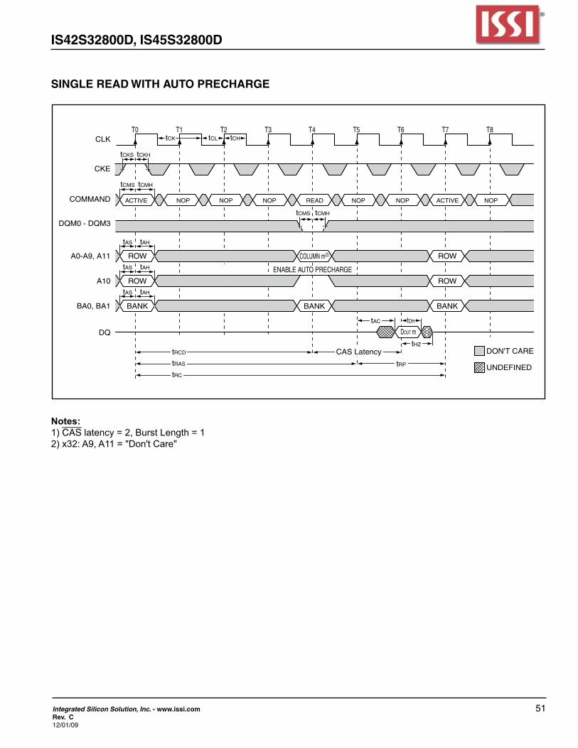
Integrated Silicon Solution, Inc. - www.issi.com 51Rev. C12/01/09
SINGLE READ WITH AUTO PRECHARGE
DON'T CARE
UNDEFINED
CLK
CKE
COMMAND
DQM0 - DQM3
A0-A9, A11
A10
BA0, BA1
DQ
tCMS tCMH
ACTIVE NOP NOP NOP READ NOP NOP ACTIVE NOP
tAS tAH
tAS tAH
tAS tAH
ROW
ROW
BANK
COLUMN m(2)
tCHtCLtCK
tCMS tCMH
tCKS tCKH
BANK
tRCD
tRAS
tRC
CAS Latency
tAC
tHZ
tOH
DOUT m
T0 T1 T2 T3 T4 T5 T6 T7 T8
tRP
ENABLE AUTO PRECHARGE
ROW
ROW
BANK
Notes:1) CAS latency = 2, Burst Length = 12) x32: A9, A11 = "Don't Care"
52 Integrated Silicon Solution, Inc. - www.issi.comRev. C
12/01/09
IS42S32800D, IS45S32800D
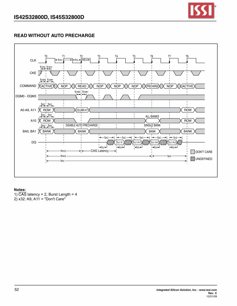
READ WITHOUT AUTO PRECHARGE
DON'T CARE
UNDEFINED
CLK
CKE
COMMAND
DQM0 - DQM3
A0-A9, A11
A10
BA0, BA1
DQ
tCMS tCMH
ACTIVE NOP READ NOP NOP NOP PRECHARGE NOP ACTIVE
tAS tAH
tAS tAH
tAS tAH
ROW
ROW
BANK
COLUMN m(2)
tCHtCLtCK
tCMS tCMH
tCKS tCKH
BANK
tRCD CAS Latency
tAC tAC tAC tAC
tOH
tHZ
tOH
DOUT m
tOH
DOUT m+1
tOH
DOUT m+2 DOUT m+3
T0 T1 T2 T3 T4 T5 T6 T7 T8
DISABLE AUTO PRECHARGE
ROW
ROW
BANK
tLZ
tRAS
tRC
tRP
ALL BANKS
SINGLE BANK
BANK
Notes:1) CAS latency = 2, Burst Length = 42) x32: A9, A11 = "Don't Care"
IS42S32800D, IS45S32800D
Integrated Silicon Solution, Inc. - www.issi.com 53Rev. C12/01/09
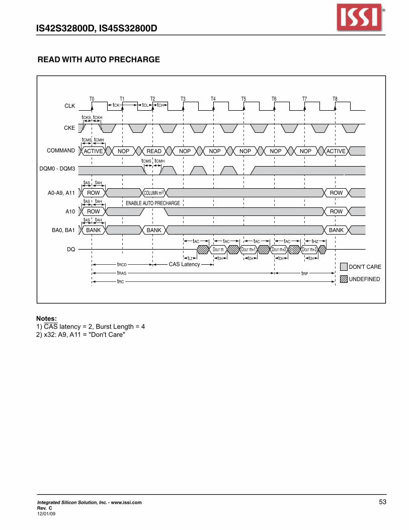
READ WITH AUTO PRECHARGE
DON'T CARE
UNDEFINED
CLK
CKE
COMMAND
DQM0 - DQM3
A0-A9, A11
A10
BA0, BA1
DQ
tCMS tCMH
ACTIVE NOP READ NOP NOP NOP NOP NOP ACTIVE
tAS tAH
tAS tAH
tAS tAH
ROW
ROW
BANK
COLUMN m(2)
tCHtCLtCK
tCMS tCMH
tCKS tCKH
BANK
tRCD
tRAS
tRC
CAS Latency
tAC tAC tAC tAC
tOH
tHZ
tOH
DOUT m
tOH
DOUT m+1
tOH
DOUT m+2 DOUT m+3
T0 T1 T2 T3 T4 T5 T6 T7 T8
tRP
ENABLE AUTO PRECHARGE
ROW
ROW
BANK
tLZ
Notes:1) CAS latency = 2, Burst Length = 42) x32: A9, A11 = "Don't Care"
54 Integrated Silicon Solution, Inc. - www.issi.comRev. C
12/01/09
IS42S32800D, IS45S32800D
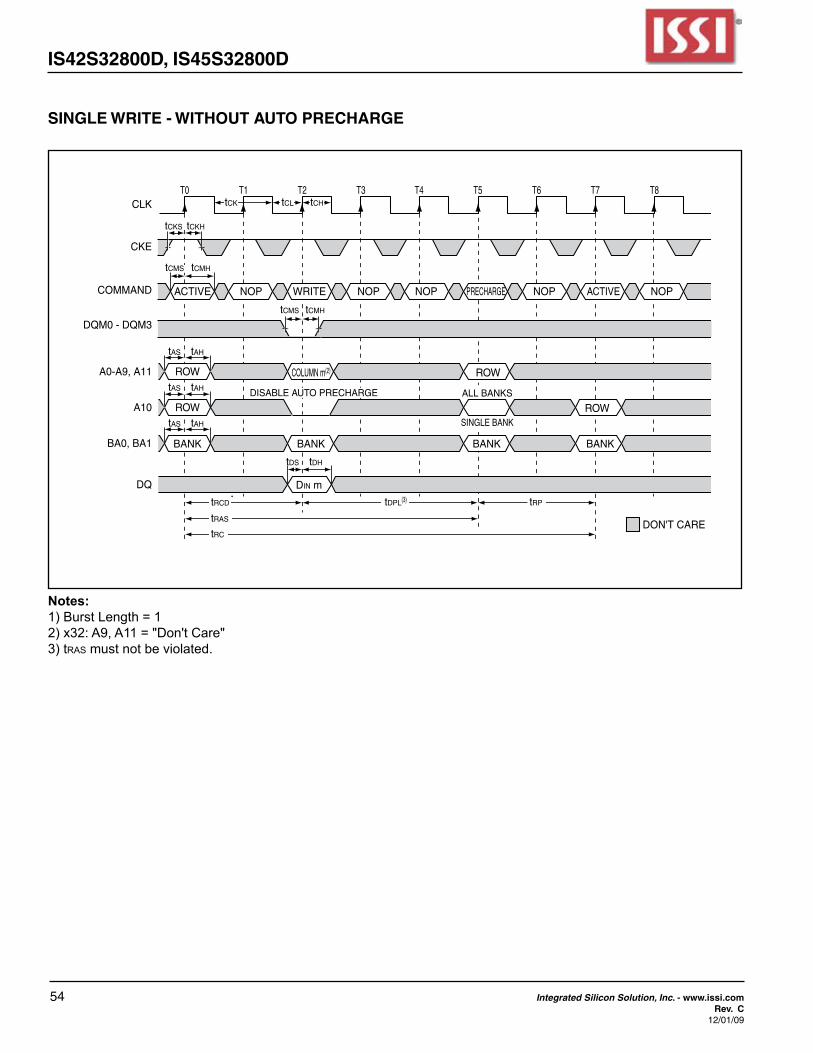
SINGLE WRITE - WITHOUT AUTO PRECHARGE
DON'T CARE
CLK
CKE
COMMAND
DQM0 - DQM3
A0-A9, A11
A10
BA0, BA1
DQ
tCMS tCMH
tAS tAH
tAS tAH
tAS tAH
tDS tDH
tRCD
tRAS
tRC
tCHtCLtCK
tCMS tCMH
tCKS tCKH
ACTIVE NOP WRITE NOP NOP PRECHARGE NOP ACTIVE NOP
tDPL(3) tRP
ROW
ROW
ROW
BANK
DIN m
COLUMN m(2) ROW
BANK BANK BANK
ALL BANKS
SINGLE BANK
T0 T1 T2 T3 T4 T5 T6 T7 T8
DISABLE AUTO PRECHARGE
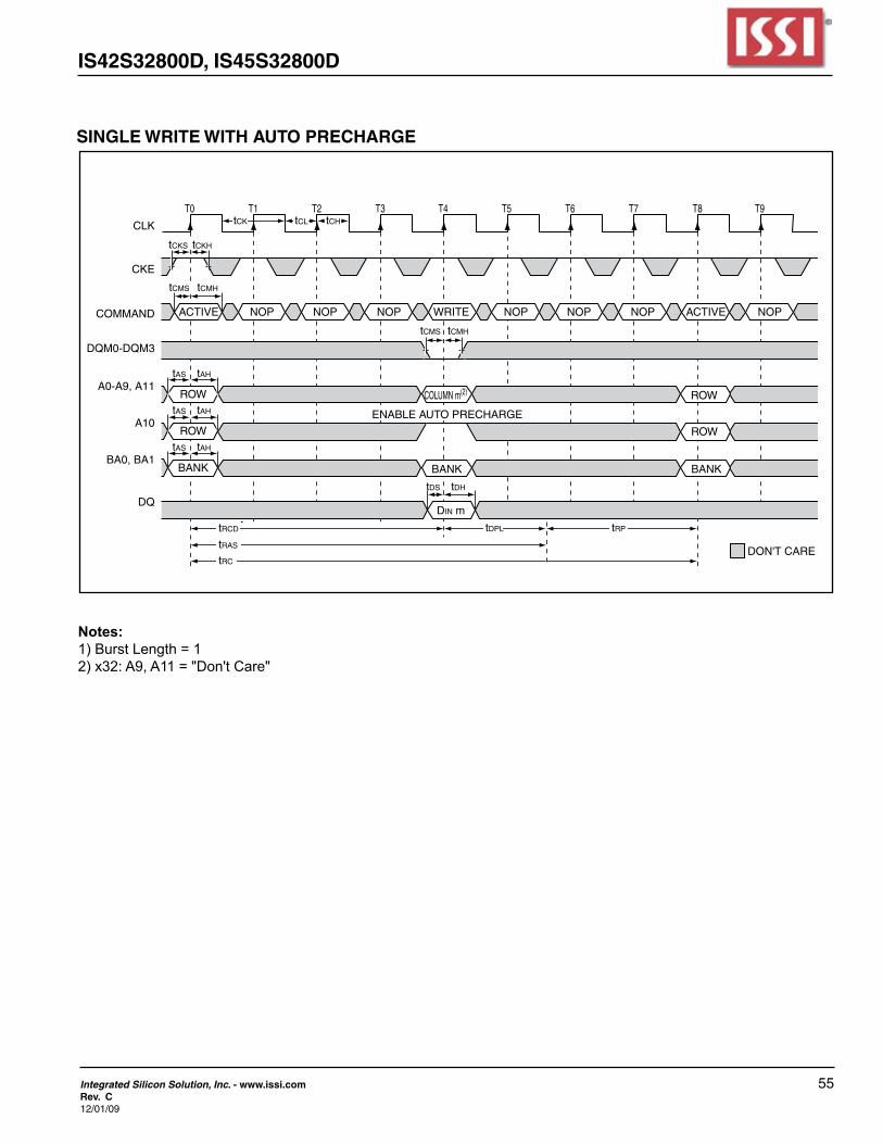
Notes:1) Burst Length = 12) x32: A9, A11 = "Don't Care"3) tras must not be violated.
IS42S32800D, IS45S32800D
Integrated Silicon Solution, Inc. - www.issi.com 55Rev. C12/01/09
SINGLE WRITE WITH AUTO PRECHARGE
Notes:1) Burst Length = 12) x32: A9, A11 = "Don't Care"
DON'T CARE
CLK
CKE
COMMAND
DQM0-DQM3
A0-A9, A11
A10
BA0, BA1
DQ
tCMS tCMH
tAS tAH
tAS tAH
tAS tAH
tDS tDH
tRCD
tRAS
tRC
tCHtCLtCK
tCMS tCMH
tCKS tCKH
ACTIVE NOP NOP NOP WRITE NOP NOP NOP ACTIVE NOP
tDPL tRP
COLUMN m(2) ROW
BANK BANK
ENABLE AUTO PRECHARGE
ROW
ROW
ROW
BANK
DIN m
T0 T1 T2 T3 T4 T5 T6 T7 T8 T9
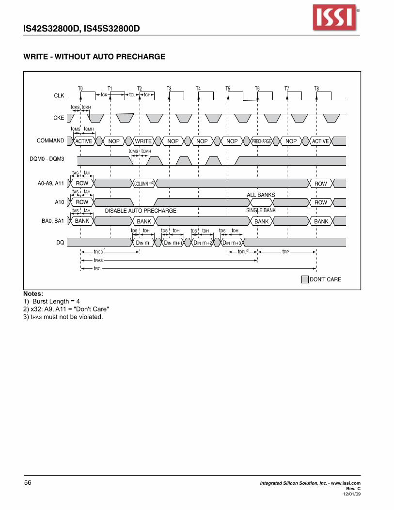
56 Integrated Silicon Solution, Inc. - www.issi.comRev. C
12/01/09
IS42S32800D, IS45S32800D
WRITE - WITHOUT AUTO PRECHARGE
DON'T CARE
CLK
CKE
COMMAND
DQM0 - DQM3
A0-A9, A11
A10
BA0, BA1
DQ
tCMS tCMH
tAS tAH
tAS tAH
tAS tAH
tRCD
tRAS
tRC
tCHtCLtCK
tCMS tCMH
tCKS tCKH
ACTIVE NOP WRITE NOP NOP NOP PRECHARGE NOP ACTIVE
tDPL(3) tRP
COLUMN m(2) ROW
DISABLE AUTO PRECHARGEROW
ROW
ROW
BANK
tDS tDH tDS tDH tDS tDHtDS tDH
DIN m DIN m+1 DIN m+2 DIN m+3
BANK BANK BANK
ALL BANKS
SINGLE BANK
T0 T1 T2 T3 T4 T5 T6 T7 T8
Notes:1) Burst Length = 42) x32: A9, A11 = "Don't Care"3) tras must not be violated.
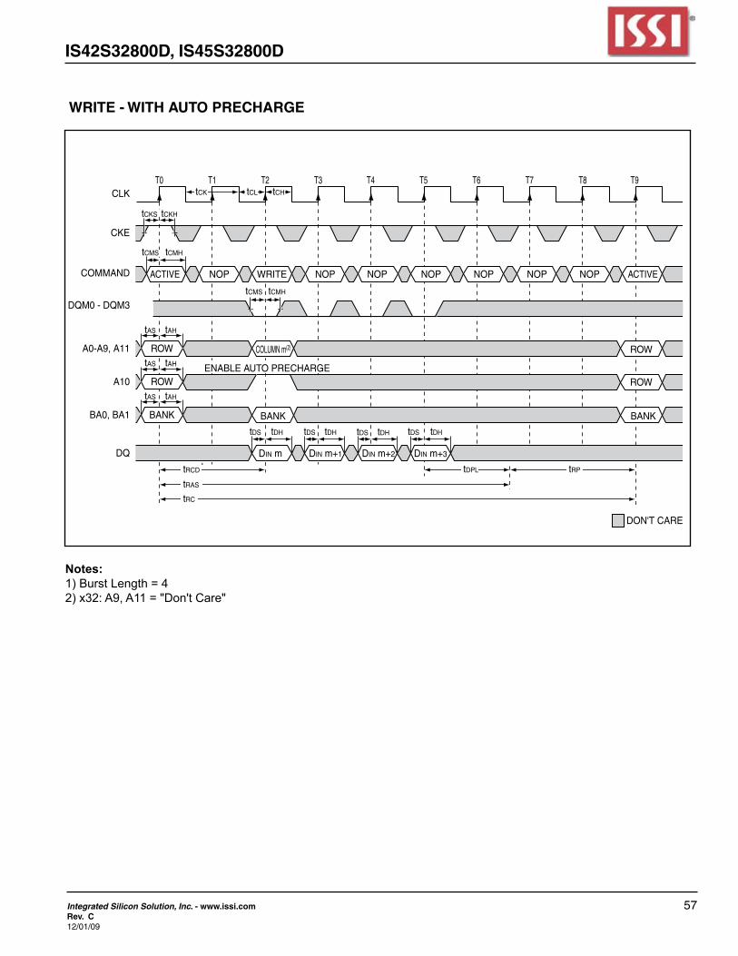
IS42S32800D, IS45S32800D
Integrated Silicon Solution, Inc. - www.issi.com 57Rev. C12/01/09
WRITE - WITH AUTO PRECHARGE
DON'T CARE
CLK
CKE
COMMAND
DQM0 - DQM3
A0-A9, A11
A10
BA0, BA1
DQ
tCMS tCMH
tAS tAH
tAS tAH
tAS tAH
tRCD
tRAS
tRC
tCHtCLtCK
tCMS tCMH
tCKS tCKH
ACTIVE NOP WRITE NOP NOP NOP NOP NOP NOP ACTIVE
tDPL tRP
COLUMN m(2) ROW
BANK BANK
ENABLE AUTO PRECHARGEROW
ROW
ROW
BANK
tDS tDH tDS tDH tDS tDHtDS tDH
DIN m DIN m+1 DIN m+2 DIN m+3
T0 T1 T2 T3 T4 T5 T6 T7 T8 T9
Notes:1) Burst Length = 42) x32: A9, A11 = "Don't Care"
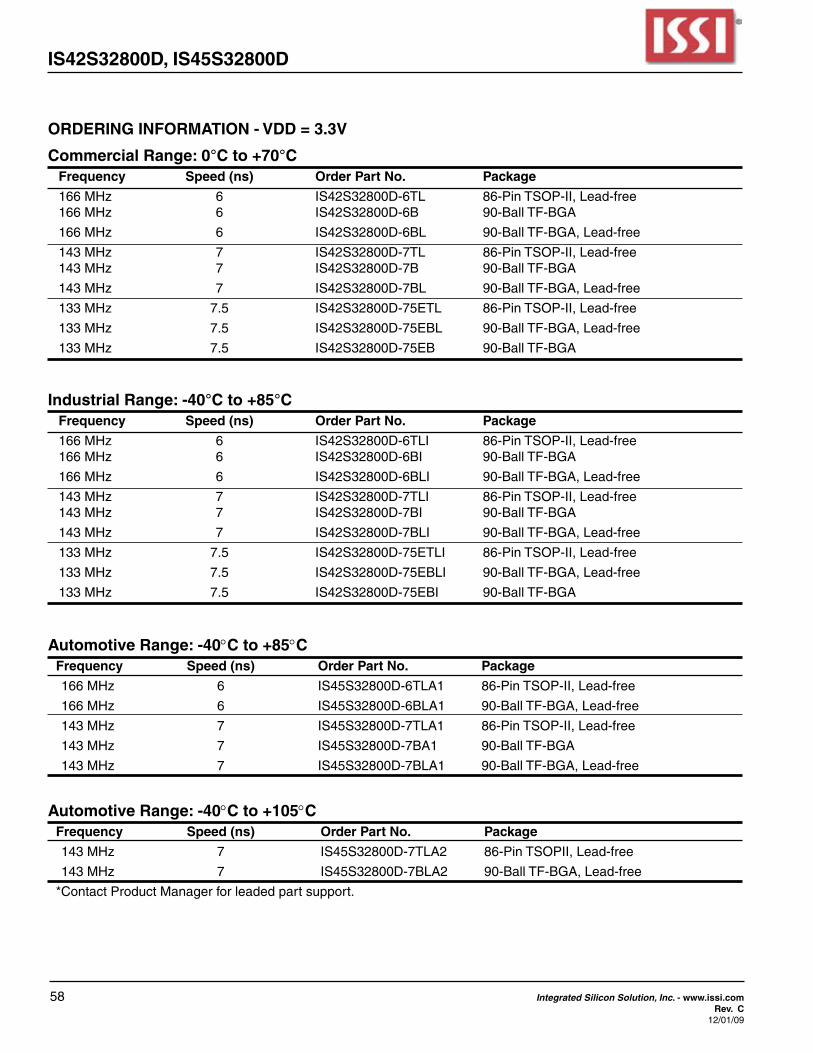
58 Integrated Silicon Solution, Inc. - www.issi.comRev. C
12/01/09
IS42S32800D, IS45S32800D
Automotive Range: -40°C to +85°C Frequency Speed (ns) Order Part No. Package
166MHz 6 IS45S32800D-6TLA1 86-PinTSOP-II,Lead-free
166MHz 6 IS45S32800D-6BLA1 90-BallTF-BGA,Lead-free
143MHz 7 IS45S32800D-7TLA1 86-PinTSOP-II,Lead-free
143MHz 7 IS45S32800D-7BA1 90-BallTF-BGA
143MHz 7 IS45S32800D-7BLA1 90-BallTF-BGA,Lead-free
Automotive Range: -40°C to +105°C Frequency Speed (ns) Order Part No. Package
143MHz 7 IS45S32800D-7TLA2 86-PinTSOPII,Lead-free
143MHz 7 IS45S32800D-7BLA2 90-BallTF-BGA,Lead-free
*ContactProductManagerforleadedpartsupport.
ORDERING INFORMATION - VDD = 3.3V
Commercial Range: 0°C to +70°C Frequency Speed (ns) Order Part No. Package
166MHz 6 IS42S32800D-6TL 86-PinTSOP-II,Lead-free 166MHz 6 IS42S32800D-6B 90-BallTF-BGA
166MHz 6 IS42S32800D-6BL 90-BallTF-BGA,Lead-free
143MHz 7 IS42S32800D-7TL 86-PinTSOP-II,Lead-free 143MHz 7 IS42S32800D-7B 90-BallTF-BGA
143MHz 7 IS42S32800D-7BL 90-BallTF-BGA,Lead-free
133MHz 7.5 IS42S32800D-75ETL 86-PinTSOP-II,Lead-free
133MHz 7.5 IS42S32800D-75EBL 90-BallTF-BGA,Lead-free
133MHz 7.5 IS42S32800D-75EB 90-BallTF-BGA
Industrial Range: -40°C to +85°C Frequency Speed (ns) Order Part No. Package
166MHz 6 IS42S32800D-6TLI 86-PinTSOP-II,Lead-free 166MHz 6 IS42S32800D-6BI 90-BallTF-BGA
166MHz 6 IS42S32800D-6BLI 90-BallTF-BGA,Lead-free
143MHz 7 IS42S32800D-7TLI 86-PinTSOP-II,Lead-free 143MHz 7 IS42S32800D-7BI 90-BallTF-BGA
143MHz 7 IS42S32800D-7BLI 90-BallTF-BGA,Lead-free
133MHz 7.5 IS42S32800D-75ETLI 86-PinTSOP-II,Lead-free
133MHz 7.5 IS42S32800D-75EBLI 90-BallTF-BGA,Lead-free
133MHz 7.5 IS42S32800D-75EBI 90-BallTF-BGA
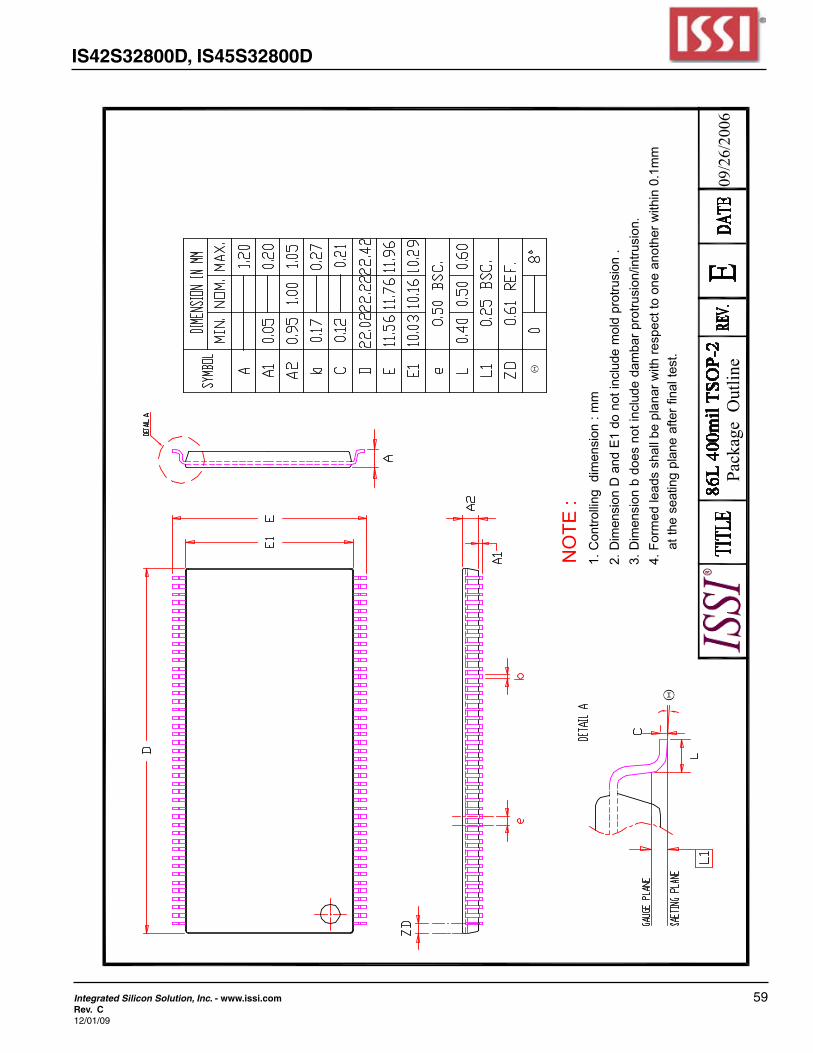
IS42S32800D, IS45S32800D
Integrated Silicon Solution, Inc. - www.issi.com 59Rev. C12/01/09
NO
TE :
Θ
Θ
4. F
orm
ed le
ads
shal
l be
plan
ar w
ith re
spec
t to
one
anot
her w
ithin
0.1
mm
2. D
imen
sion
D a
nd E
1 do
not
incl
ude
mol
d pr
otru
sion
.
at t
he s
eatin
g pl
ane
afte
r fin
al te
st.
1. C
ontro
lling
dim
ensi
on :
mm
3. D
imen
sion
b d
oes
not i
nclu
de d
amba
r pro
trusi
on/in
trusi
on.
09/2
6/20
06Pa
ckag
e O
utlin
e
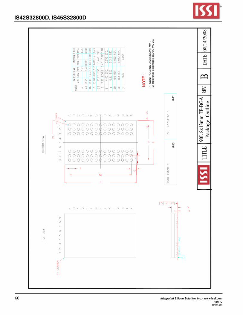
60 Integrated Silicon Solution, Inc. - www.issi.comRev. C
12/01/09
IS42S32800D, IS45S32800D
0.45
0.80
D1
2. R
efer
ence
doc
umen
t : J
ED
EC
MO
-207
1. C
ON
TRO
LLIN
G D
IMEN
SIO
N :
MM
.
NO
TE :
Pack
age
Out
line
08/1
4/20
08