Embed Size (px)
Citation preview
SDRAMAS4SD16M16
AS4SD16M16Rev. 2.6 04/13/15
Micross Components reserves the right to change products or specifications without notice.
1
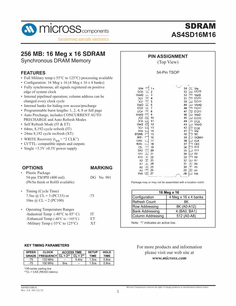
FEATURES• Full Military temp (-55°C to 125°C) processing available• Configuration: 16 Meg x 16 (4 Meg x 16 x 4 banks)• Fully synchronous; all signals registered on positive edge of system clock• Internal pipelined operation; column address can be changed every clock cycle• Internal banks for hiding row access/precharge• Programmable burst lengths: 1, 2, 4, 8 or full page• Auto Precharge, includes CONCURRENT AUTO PRECHARGE and Auto Refresh Modes• Self Refresh Mode (IT & ET)• 64ms, 8,192-cycle refresh (IT)• 24ms 8,192 cycle recfresh (XT)• WRITE Recovery (tWR = “2 CLK”)• LVTTL- compatible inputs and outputs• Single +3.3V ±0.3V power supply
OPTIONS MARKING• Plastic Package 54-pin TSOPII (400 mil) DG No. 901 (Pb/Sn finish or RoHS available)
• Timing (Cycle Time) 7.5ns @ CL = 3 (PC133) or -75 10ns @ CL = 2 (PC100)
• Operating Temperature Ranges -Industrial Temp (-40°C to 85° C) IT -Enhanced Temp (-40°C to +105°C) ET -Military Temp (-55°C to 125°C) XT
*Off-center parting line**CL = CAS (READ) latency
Package may or may not be assembled with a location notch.
PIN ASSIGNMENT (Top View)
54-Pin TSOP
Note: “\” indicates an active low.
256 MB: 16 Meg x 16 SDRAMSynchronous DRAM Memory
For more products and informationplease visit our web site at
www.micross.com
KEY TIMING PARAMETERS
SPEED CLOCK SETUP HOLDGRADE FREQUENCY CL = 2** CL = 3** TIME TIME
-75 133 MHz – 5.4ns 1.5ns 0.8ns-75 100 MHz 6ns – 1.5ns 0.8ns
ACCESS TIME
Configuration 4 Meg x 16 x 4 banksRefresh Count 8KRow Addressing 8K (A0-A12)Bank Addressing 4 (BA0, BA1)Column Addressing 512 (A0-A8)
16 Meg x 16
SDRAMAS4SD16M16
AS4SD16M16Rev. 2.6 04/13/15
Micross Components reserves the right to change products or specifications without notice.
2
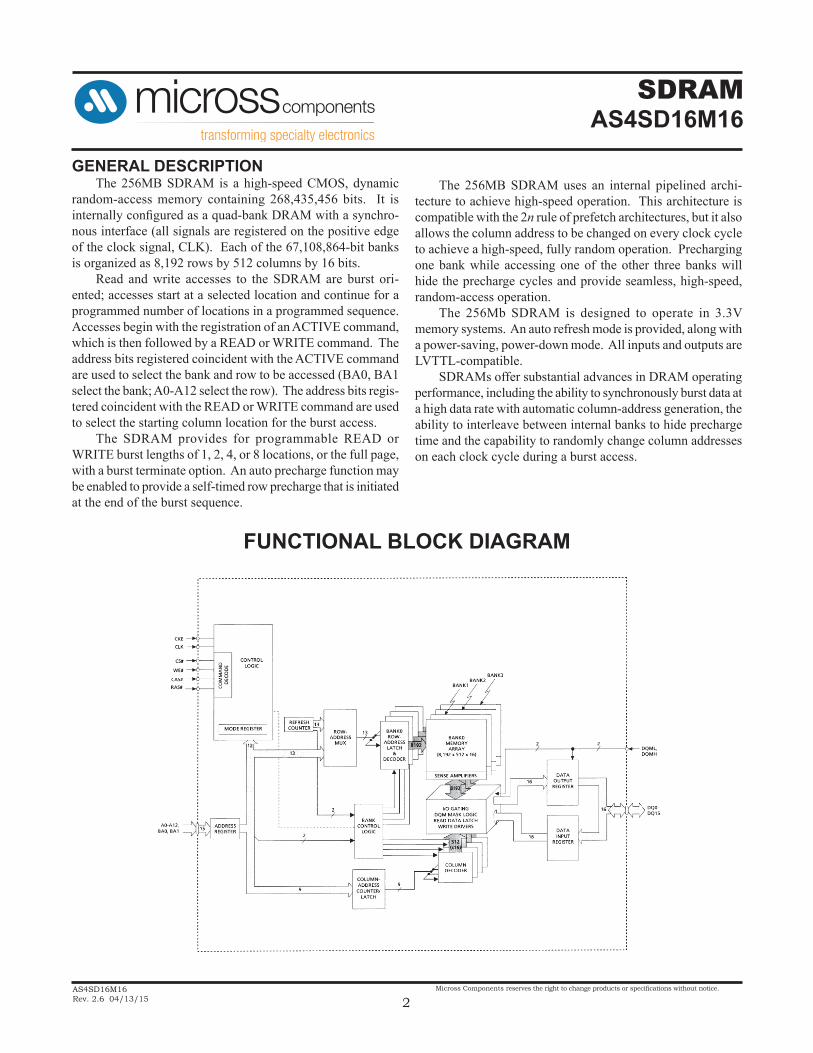
GENERAL DESCRIPTION The 256MB SDRAM is a high-speed CMOS, dynamic random-access memory containing 268,435,456 bits. It is internally configured as a quad-bank DRAM with a synchro-nous interface (all signals are registered on the positive edge of the clock signal, CLK). Each of the 67,108,864-bit banks is organized as 8,192 rows by 512 columns by 16 bits. Read and write accesses to the SDRAM are burst ori-ented; accesses start at a selected location and continue for a programmed number of locations in a programmed sequence. Accesses begin with the registration of an ACTIVE command, which is then followed by a READ or WRITE command. The address bits registered coincident with the ACTIVE command are used to select the bank and row to be accessed (BA0, BA1 select the bank; A0-A12 select the row). The address bits regis-tered coincident with the READ or WRITE command are used to select the starting column location for the burst access. The SDRAM provides for programmable READ or WRITE burst lengths of 1, 2, 4, or 8 locations, or the full page, with a burst terminate option. An auto precharge function may be enabled to provide a self-timed row precharge that is initiated at the end of the burst sequence.
The 256MB SDRAM uses an internal pipelined archi-tecture to achieve high-speed operation. This architecture is compatible with the 2n rule of prefetch architectures, but it also allows the column address to be changed on every clock cycle to achieve a high-speed, fully random operation. Precharging one bank while accessing one of the other three banks will hide the precharge cycles and provide seamless, high-speed, random-access operation. The 256Mb SDRAM is designed to operate in 3.3V memory systems. An auto refresh mode is provided, along with a power-saving, power-down mode. All inputs and outputs are LVTTL-compatible. SDRAMs offer substantial advances in DRAM operating performance, including the ability to synchronously burst data at a high data rate with automatic column-address generation, the ability to interleave between internal banks to hide precharge time and the capability to randomly change column addresses on each clock cycle during a burst access.
FUNCTIONAL BLOCK DIAGRAM
SDRAMAS4SD16M16
AS4SD16M16Rev. 2.6 04/13/15
Micross Components reserves the right to change products or specifications without notice.
3
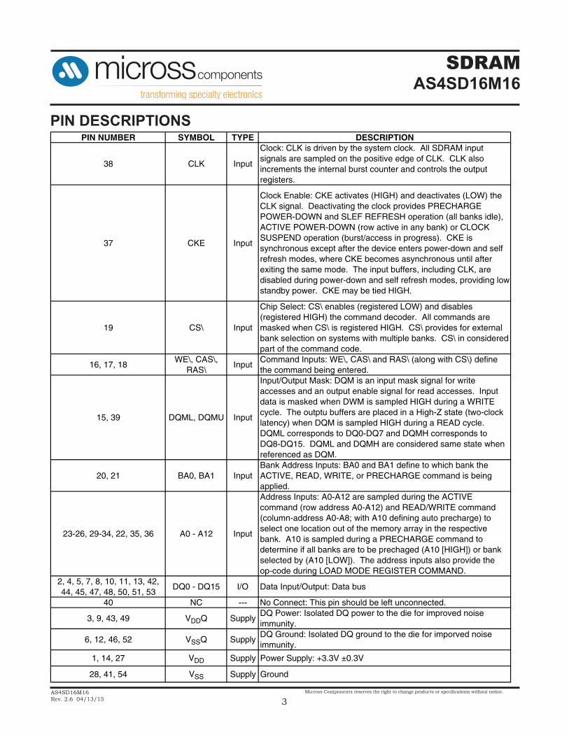
PIN NUMBER SYMBOL TYPE DESCRIPTION
38 CLK Input
Clock: CLK is driven by the system clock. All SDRAM input signals are sampled on the positive edge of CLK. CLK also increments the internal burst counter and controls the output registers.
37 CKE Input
Clock Enable: CKE activates (HIGH) and deactivates (LOW) the CLK signal. Deactivating the clock provides PRECHARGE POWER-DOWN and SLEF REFRESH operation (all banks idle), ACTIVE POWER-DOWN (row active in any bank) or CLOCK SUSPEND operation (burst/access in progress). CKE is synchronous except after the device enters power-down and self refresh modes, where CKE becomes asynchronous until after exiting the same mode. The input buffers, including CLK, are disabled during power-down and self refresh modes, providing low standby power. CKE may be tied HIGH.
19 CS\ Input
Chip Select: CS\ enables (registered LOW) and disables (registered HIGH) the command decoder. All commands are masked when CS\ is registered HIGH. CS\ provides for external bank selection on systems with multiple banks. CS\ in considered part of the command code.
16, 17, 18WE\, CAS\,
RAS\Input
Command Inputs: WE\, CAS\ and RAS\ (along with CS\) define the command being entered.
15, 39 DQML, DQMU Input
Input/Output Mask: DQM is an input mask signal for write accesses and an output enable signal for read accesses. Input data is masked when DWM is sampled HIGH during a WRITE cycle. The outptu buffers are placed in a High-Z state (two-clock latency) when DQM is sampled HIGH during a READ cycle. DQML corresponds to DQ0-DQ7 and DQMH corresponds to DQ8-DQ15. DQML and DQMH are considered same state when referenced as DQM.
20, 21 BA0, BA1 InputBank Address Inputs: BA0 and BA1 define to which bank the ACTIVE, READ, WRITE, or PRECHARGE command is being applied.
23-26, 29-34, 22, 35, 36 A0 - A12 Input
Address Inputs: A0-A12 are sampled during the ACTIVE command (row address A0-A12) and READ/WRITE command (column-address A0-A8; with A10 defining auto precharge) to select one location out of the memory array in the respective bank. A10 is sampled during a PRECHARGE command to determine if all banks are to be prechaged (A10 [HIGH]) or bank selected by (A10 [LOW]). The address inputs also provide the op-code during LOAD MODE REGISTER COMMAND.
2, 4, 5, 7, 8, 10, 11, 13, 42, 44, 45, 47, 48, 50, 51, 53
DQ0 - DQ15 I/O Data Input/Output: Data bus
40 NC --- No Connect: This pin should be left unconnected.
3, 9, 43, 49 VDDQ SupplyDQ Power: Isolated DQ power to the die for improved noise immunity.
6, 12, 46, 52 VSSQ SupplyDQ Ground: Isolated DQ ground to the die for imporved noise immunity.
1, 14, 27 VDD Supply Power Supply: +3.3V ±0.3V
28, 41, 54 VSS Supply Ground
PIN DESCRIPTIONS
SDRAMAS4SD16M16
AS4SD16M16Rev. 2.6 04/13/15
Micross Components reserves the right to change products or specifications without notice.
4
FUNCTIONAL DESCRIPTION In general, the 256MB SDRAMs are quad-bank DRAMs that operate at 3.3V and include a synchronous interface (all signals are registered on the positive edge of the clock signal, CLK). Each of the 67,108,864-bit banks is organized as 8,192 rows by 512 columns by 16 bits. Read and write accesses to the SDRAM are burst ori-ented; accesses start at a selected location and continue for a programmed number of locations in a programmed sequence. Accesses begin with the registration of an ACTIVE command, which is then followed by a READ or WRITE command. The address bits registered coincident with the ACTIVE command are used to select the bank and row to be accessed (BA0 and BA1 select the bank, A0 - A12 select the row). The address bits (A0 - A8) registered coincident with the READ or WRITE command are used to select the starting column location for the burst access. Prior to normal operation, the SDRAM must be initialized. The following sections provide detailed information covering device initialization, register definition, command descriptions and device operation.
Initialization SDRAMs must be powered up and initialized in a pre-defined manner. Operational procedures other than those specified may result in undefined operation. Once power is applied to VDD and VDDQ (simultaneously) and the clock is stable (stable clock is defined as a signal cycling within timing constraints specified for the clock pin), the SDRAM requires a 100µs delay prior to issuing any command other than a COM-MAND INHIBIT or NOP. Starting at some point during this 100µs period and continuing at least through the end of this period, COMMAND INHIBIT or NOP commands should be applied. Once the 100µs delay has been satisfied with at least one COMMAND INHIBIT or NOP command having been applied, a PRECHARGE command should be applied. All banks must then be precharged, thereby placing the device in the all banks idle state. Once in the idle state, two AUTO REFRESH cycles must be preformed. After the AUTO REFRESH cycles are complete, the SDRAM is ready for mode register programming. Because the mode register will power up in an unknown state, it should be loaded prior to applying any operational command.
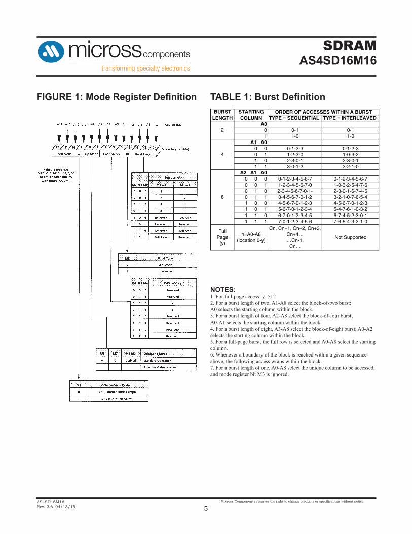
Register DefinitionMODE REGISTER The mode register is used to define the specific mode of operation of the SDRAM. This definition includes the
selection of a burst length, a burst type, a CAS latency, an operating mode and a write burst mode, as shown in Figure 1. The mode register is programmed via the LOAD MODE REGISTER command and will retain the stored information until it is programmed again or the device loses power. Mode register bits M0 - M2 specify the burst length, M3 specifies the type of burst (sequential or interleaved), M4 - M6 specify the CAS latency, M7 and M8 specify the operating mode, M9 specifies the write burst mode, and M10 and M11 are reserved for future use. Address A12 (M12) is undefined but should be driven LOW during loading of the mode register. The mode register must be loaded when all banks are idle, and the controller must wait the specified time before initiating the subsequent operation. Violating either of these requirements will result in unspecified operation.
Burst Length Read and write accesses to the SDRAM are burst oriented, with the burst length being programmable, as shown in Figure 1. The burst length determines the maximum number of column locations that can be accessed for a given READ or WRITE command. Burst lengths of 1, 2, 4, or 8 locations are available for both the sequential and the interleaved burst types, and a full-page burst is available for the sequential types. The full-page burst is used in conjunction with the BURST TERMINATE command to generate arbitrary burst lengths. Reserved states should not be used as unknown operation or incompatibility with future versions may result. When a READ or WRITE command is issued, a block of columns equal to the burst length is effectively selected. All accesses for that burst take place within this block, mean-ing that the burst will wrap within the block if a boundary is reached. The clock is uniquely selected by A1-A8 when the burst length is set to two; by A2-A8 when the burst length is set to four, and by A3-A8 when the burst length is set to eight. The remaining (least significant) address bit(s) is (are) used to select the starting location within the block. Full-page bursts wrap within the page if the boundary is reached.
Burst Type Accesses within a given burst may be programmed to be either sequential or interleaved; this is referred to as the burst type and is selected via bit M3. The ordering of accesses within a burst is determined by the burst length, the burst type and the starting column address, shown in table 1.
SDRAMAS4SD16M16
AS4SD16M16Rev. 2.6 04/13/15
Micross Components reserves the right to change products or specifications without notice.
5
FIGURE 1: Mode Register Definition TABLE 1: Burst Definition
TYPE = SEQUENTIAL TYPE = INTERLEAVEDA0
0 0-1 0-11 1-0 1-0
A1 A00 0 0-1-2-3 0-1-2-30 1 1-2-3-0 1-0-3-21 0 2-3-0-1 2-3-0-11 1 3-0-1-2 3-2-1-0
A2 A1 A00 0 0 0-1-2-3-4-5-6-7 0-1-2-3-4-5-6-70 0 1 1-2-3-4-5-6-7-0 1-0-3-2-5-4-7-60 1 0 2-3-4-5-6-7-0-1- 2-3-0-1-6-7-4-50 1 1 3-4-5-6-7-0-1-2 3-2-1-0-7-6-5-41 0 0 4-5-6-7-0-1-2-3 4-5-6-7-0-1-2-31 0 1 5-6-7-0-1-2-3-4 5-4-7-6-1-0-3-21 1 0 6-7-0-1-2-3-4-5 6-7-4-5-2-3-0-11 1 1 7-0-1-2-3-4-5-6 7-6-5-4-3-2-1-0
Full Page
(y)
n=A0-A8 (location 0-y)
Cn, Cn+1, Cn+2, Cn+3, Cn+4… …Cn-1,
Cn…
Not Supported
4
8
BURST LENGTH
STARTING COLUMN
ORDER OF ACCESSES WITHIN A BURST
2
NOTES:1. For full-page access: y=5122. For a burst length of two, A1-A8 select the block-of-two burst; A0 selects the starting column within the block.3. For a burst length of four, A2-A8 select the block-of-four burst; A0-A1 selects the starting column within the block.4. For a burst length of eight, A3-A8 select the block-of-eight burst; A0-A2 selects the starting column within the block.5. For a full-page burst, the full row is selected and A0-A8 select the starting column.6. Whenever a boundary of the block is reached within a given sequence above, the following access wraps within the block.7. For a burst length of one, A0-A8 select the unique column to be accessed, and mode register bit M3 is ignored.
SDRAMAS4SD16M16
AS4SD16M16Rev. 2.6 04/13/15
Micross Components reserves the right to change products or specifications without notice.
6
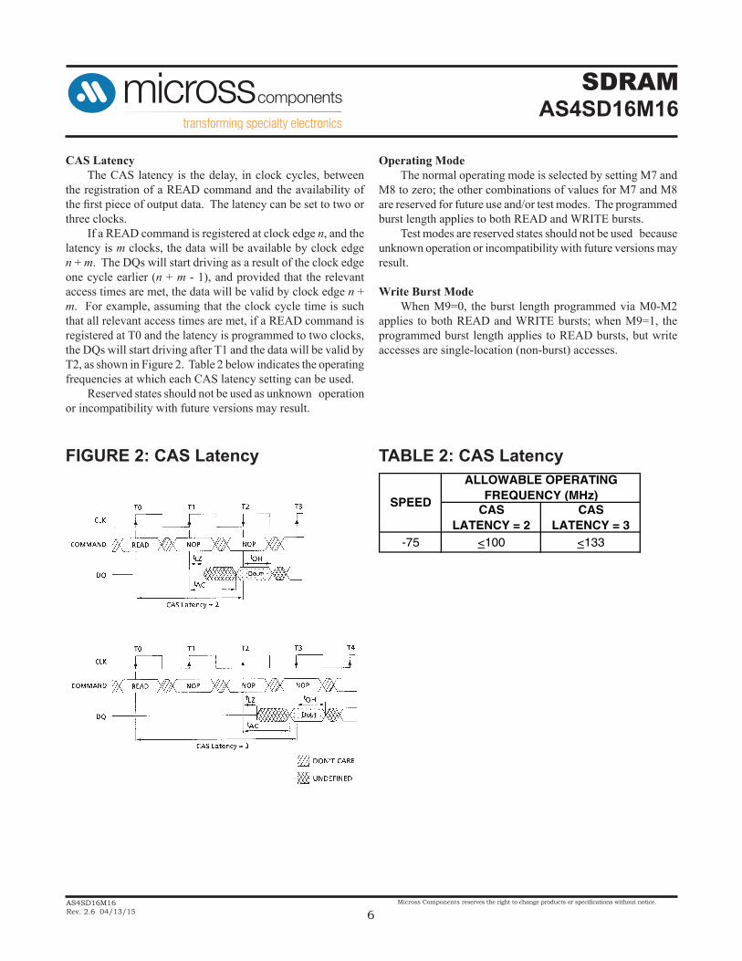
CAS Latency The CAS latency is the delay, in clock cycles, between the registration of a READ command and the availability of the first piece of output data. The latency can be set to two or three clocks. If a READ command is registered at clock edge n, and the latency is m clocks, the data will be available by clock edge n + m. The DQs will start driving as a result of the clock edge one cycle earlier (n + m - 1), and provided that the relevant access times are met, the data will be valid by clock edge n + m. For example, assuming that the clock cycle time is such that all relevant access times are met, if a READ command is registered at T0 and the latency is programmed to two clocks, the DQs will start driving after T1 and the data will be valid by T2, as shown in Figure 2. Table 2 below indicates the operating frequencies at which each CAS latency setting can be used. Reserved states should not be used as unknown operation or incompatibility with future versions may result.
Operating Mode The normal operating mode is selected by setting M7 and M8 to zero; the other combinations of values for M7 and M8 are reserved for future use and/or test modes. The programmed burst length applies to both READ and WRITE bursts. Test modes are reserved states should not be used because unknown operation or incompatibility with future versions may result.
Write Burst Mode When M9=0, the burst length programmed via M0-M2 applies to both READ and WRITE bursts; when M9=1, the programmed burst length applies to READ bursts, but write accesses are single-location (non-burst) accesses.
FIGURE 2: CAS Latency TABLE 2: CAS Latency
CAS LATENCY = 2
CAS LATENCY = 3
-75 <100 <133
SPEED
ALLOWABLE OPERATING FREQUENCY (MHz)
SDRAMAS4SD16M16
AS4SD16M16Rev. 2.6 04/13/15
Micross Components reserves the right to change products or specifications without notice.
7
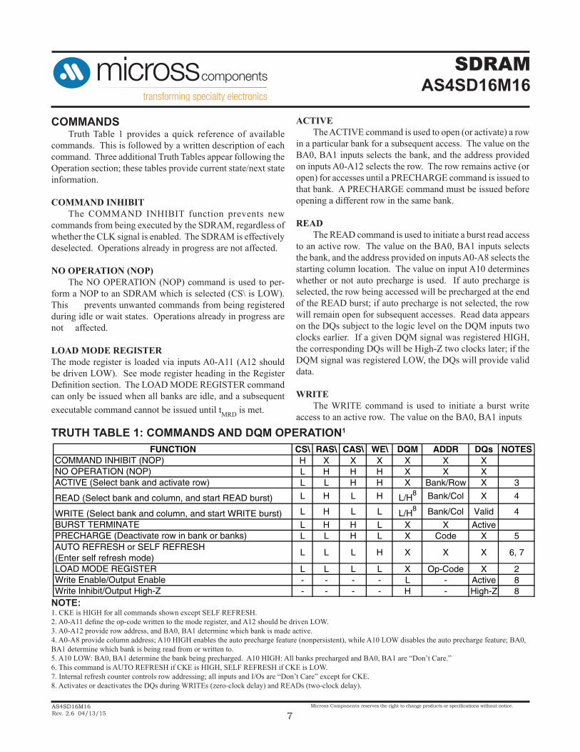
COMMANDS Truth Table 1 provides a quick reference of available commands. This is followed by a written description of each command. Three additional Truth Tables appear following the Operation section; these tables provide current state/next state information.
COMMAND INHIBIT The COMMAND INHIBIT function prevents new commands from being executed by the SDRAM, regardless of whether the CLK signal is enabled. The SDRAM is effectively deselected. Operations already in progress are not affected.
NO OPERATION (NOP) The NO OPERATION (NOP) command is used to per-form a NOP to an SDRAM which is selected (CS\ is LOW). This prevents unwanted commands from being registered during idle or wait states. Operations already in progress are not affected.
LOAD MODE REGISTERThe mode register is loaded via inputs A0-A11 (A12 should be driven LOW). See mode register heading in the Register Definition section. The LOAD MODE REGISTER command can only be issued when all banks are idle, and a subsequent executable command cannot be issued until tMRD is met.
TRUTH TABLE 1: COMMANDS AND DQM OPERATION1
FUNCTION CS\ RAS\ CAS\ WE\ DQM ADDR DQs NOTESCOMMAND INHIBIT (NOP) H X X X X X XNO OPERATION (NOP) L H H H X X XACTIVE (Select bank and activate row) L L H H X Bank/Row X 3
READ (Select bank and column, and start READ burst) L H L H L/H8 Bank/Col X 4
WRITE (Select bank and column, and start WRITE burst) L H L L L/H8 Bank/Col Valid 4
BURST TERMINATE L H H L X X ActivePRECHARGE (Deactivate row in bank or banks) L L H L X Code X 5AUTO REFRESH or SELF REFRESH (Enter self refresh mode)
L L L H X X X 6, 7
LOAD MODE REGISTER L L L L X Op-Code X 2Write Enable/Output Enable - - - - L - Active 8Write Inhibit/Output High-Z - - - - H - High-Z 8
NOTE:1. CKE is HIGH for all commands shown except SELF REFRESH.2. A0-A11 define the op-code written to the mode register, and A12 should be driven LOW.3. A0-A12 provide row address, and BA0, BA1 determine which bank is made active.4. A0-A8 provide column address; A10 HIGH enables the auto precharge feature (nonpersistent), while A10 LOW disables the auto precharge feature; BA0, BA1 determine which bank is being read from or written to.5. A10 LOW: BA0, BA1 determine the bank being precharged. A10 HIGH: All banks precharged and BA0, BA1 are “Don’t Care.”6. This command is AUTO REFRESH if CKE is HIGH, SELF REFRESH if CKE is LOW.7. Internal refresh counter controls row addressing; all inputs and I/Os are “Don’t Care” except for CKE.8. Activates or deactivates the DQs during WRITEs (zero-clock delay) and READs (two-clock delay).
ACTIVE The ACTIVE command is used to open (or activate) a row in a particular bank for a subsequent access. The value on the BA0, BA1 inputs selects the bank, and the address provided on inputs A0-A12 selects the row. The row remains active (or open) for accesses until a PRECHARGE command is issued to that bank. A PRECHARGE command must be issued before opening a different row in the same bank.
READ The READ command is used to initiate a burst read access to an active row. The value on the BA0, BA1 inputs selects the bank, and the address provided on inputs A0-A8 selects the starting column location. The value on input A10 determines whether or not auto precharge is used. If auto precharge is selected, the row being accessed will be precharged at the end of the READ burst; if auto precharge is not selected, the row will remain open for subsequent accesses. Read data appears on the DQs subject to the logic level on the DQM inputs two clocks earlier. If a given DQM signal was registered HIGH, the corresponding DQs will be High-Z two clocks later; if the DQM signal was registered LOW, the DQs will provide valid data.
WRITE The WRITE command is used to initiate a burst write access to an active row. The value on the BA0, BA1 inputs
SDRAMAS4SD16M16
AS4SD16M16Rev. 2.6 04/13/15
Micross Components reserves the right to change products or specifications without notice.
8
WRITE (continued)selects the bank, and the address provided on inputs A0-A8 selects the starting column location. The value on input A10 determines whether or not auto precharge is used. If auto pre-charge is selected, the row being accessed will be precharged at the end of the WRITE burst; if auto precharge is not selected, the row will remain open for subsequent accesses. Input data appearing on the DQs is written to the memory array subject to the DQM input logic level appearing coincident with the data. If a given DQM signal is registered LOW, the corresponding data will be written to memory; if the DQM signal is registered HIGH, the corresponding data inputs will be ignored, and a WRITE will not be executed to that byte/column location.
PRECHARGE The PRECHARGE command is used to deactivate the open row in a particular bank or the open row in all banks. The bank(s) will be available for a subsequent row access a specified time (tRP) after the PRECHARGE command is issued. Input A10 determines whether one or all banks are to be precharged, an in the case where only one bank is to be precharged, inputs BA0, BA1 select the bank. Otherwise BA0, BA1 are treated as “Don’t Care.” Once a bank has been precharged, it is in the idle state and must be activated prior to any READ or WRITE commands being issued to that bank.
AUTO PRECHARGE Auto precharge is a feature which performs the same individual-bank PRECHARGE functions described above, without requiring an explicit command. This is accomplished by using A10 to enable auto precharge in conjunction with a specific READ or WRITE command. A PRECHARGE of the bank/row that is addressed with the READ or WRITE command is automatically performed upon completion of the READ or WRITE burst, except in the full-page burst mode, where AUTO PRECHARGE does not apply. Auto precharge is nonpersistent in that it is either enabled or disabled for each individual READ or WRITE command. Auto precharge ensures that the precharge is initiated at the earliest valid stage within a burst. The user must not issue another command to the same bank until the precharge time (tRP) is completed. This is determined as if an explicit PRE-CHARGE command was issued at the earliest possible time, as described for each burst type in the Operation section of this data sheet.
BURST TERMINATE The BURST TERMINATE command is used to truncate either fixed-length or full-page bursts. The most recently registered READ or WRITE command prior to the BURST
TERMINATE command will be truncated, as shown in the Operation section of this data sheet.
AUTO REFRESH AUTO REFRESH is used during normal operation of the SDRAM and is analogous to CAS\-BEFORE-RAS\ (CBR) REFRESH in conventional DRAMs. This command is non-persistent, so it must be issued each time a refresh is required. All active banks must be precharged prior to issuing an AUTO REFRESH command. The AUTO REFRESH command should not be issued until the minimum tRP has been met after the PRECHARGE command as shown in the Operations sec-tion. The addressing is generated by the internal refresh con-troller. This makes the address bits “Don’t Care” during an AUTO REFRESH command. The 256MB SDRAM requires 8,192 AUTO REFRESH cycles every 64ms (tREF), regardless of width operation. Providing a distributed AUTO REFRESH command every 7.81µs will meet the refresh requirement and ensure that each row is refreshed. Alternatively, 8,192 AUTO REFRESH commands can be issued in a burst at the minimum cycle rate (tRFC), once every 64ms (24ms for XT version)
SELF REFRESH (IT & ET Temp options ONLY) The SELF REFRESH command can be used to retain data in the SDRAM, even if the rest of the system is powered down. When in the self refresh mode, the SDRAM retains data without external clocking. The SELF REFRESH command is initiated like and AUTO REFRESH command except CKE is disabled (LOW). Once the SELF REFRESH command is registered, all the inputs to the SDRAM become “Don’t Care” with the exception of CKE, which must remain LOW. Once self refresh mode is engaged, the SDRAM provides its own internal clocking, causing it to perform its own AUTO REFRESH cycles. The SDRAM must remain in self refresh mode for a minimum period equal to tRAS and may remain in self refresh mode for an indefinite period beyond that. The procedure for exiting self refresh requires a sequence of commands. First, CLK must be stable (stable clock is de-fined as a signal cycling within timing constraints specified for the clock pin) prior to CKE going back HIGH. Once CKE is HIGH, the SDRAM must have NOP commands issued (a minimum of two clocks) for tXSR because time is required for the completion of any internal refresh in progress. Upon exiting the self refresh mode, AUTO REFRESH commands must be issued every 7.81µs or less as both SELF REFRESH and AUTO REFRESH utilize the row refresh coun-ter. The SELF REFRESH and AUTO REFRESH option are available with the IT and ET temperature options. They are not available with the XT temperature options.
SDRAMAS4SD16M16
AS4SD16M16Rev. 2.6 04/13/15
Micross Components reserves the right to change products or specifications without notice.
9
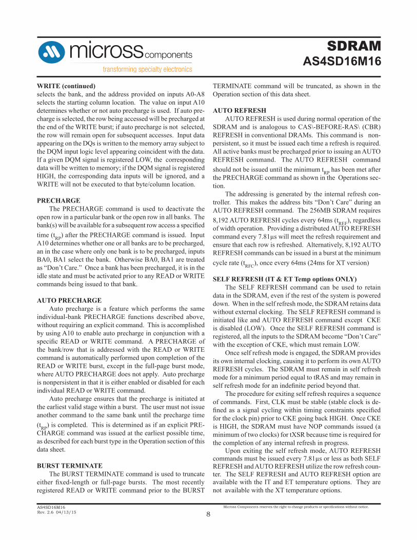
OPERATIONBANK/ROW ACTIVATION Before any READ or WRITE commands can be issued to a bank within the SDRAM, a row in that bank must be “opened.” This is accomplished via the ACTIVE command, which selects both the bank and the row to be activated (see Figure 3). After opening a row (issuing an ACTIVE command), a READ or WRITE command may be issued to that row, sub-ject to the tRCD specification. tRCD (MIN) should be divided by the clock period and rounded up to the next whole number to determine the earliest clock edge after the ACTIVE com-mand on which a READ or WRITE command can be entered. For example, a tRCD specification of 20ns with a 125 MHz clock (8ns period) results in 2.5 clocks, rounded to 3. This is reflected in Figure 4, which covers any case where 2 < tRCD (MIN)/ tCK < 3. (The same procedure is used to convert other specification limits from time units to clock cycles.) A subsequent ACTIVE command to a different row in the same bank can only be issued after the previous active row has been “closed” (precharged). The minimum time interval between successive ACTIVE commands to the same bank is defined by tRC. A subsequent ACTIVE command to another bank can be issued while the first bank is being accessed, which results in a reduction of total row-access overhead. The minimum time interval between successive ACTIVE commands to different banks is defined by tRRD.
FIGURE 3: Activating a Specific Row in a Specific Bank
FIGURE 4: Example - Meeting tRCD (MIN) When 2 < tRCD (MIN)/ tCK < 3
SDRAMAS4SD16M16
AS4SD16M16Rev. 2.6 04/13/15
Micross Components reserves the right to change products or specifications without notice.
10
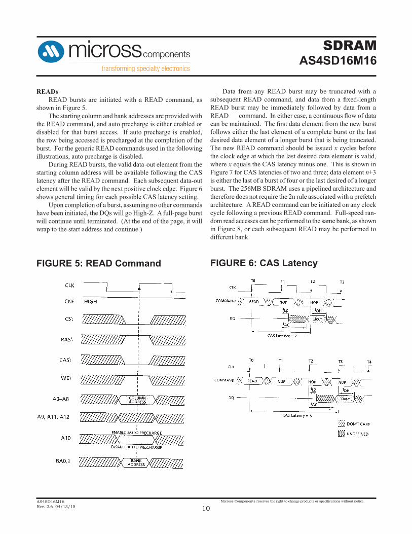
READs READ bursts are initiated with a READ command, as shown in Figure 5. The starting column and bank addresses are provided with the READ command, and auto precharge is either enabled or disabled for that burst access. If auto precharge is enabled, the row being accessed is precharged at the completion of the burst. For the generic READ commands used in the following illustrations, auto precharge is disabled. During READ bursts, the valid data-out element from the starting column address will be available following the CAS latency after the READ command. Each subsequent data-out element will be valid by the next positive clock edge. Figure 6 shows general timing for each possible CAS latency setting. Upon completion of a burst, assuming no other commands have been initiated, the DQs will go High-Z. A full-page burst will continue until terminated. (At the end of the page, it will wrap to the start address and continue.)
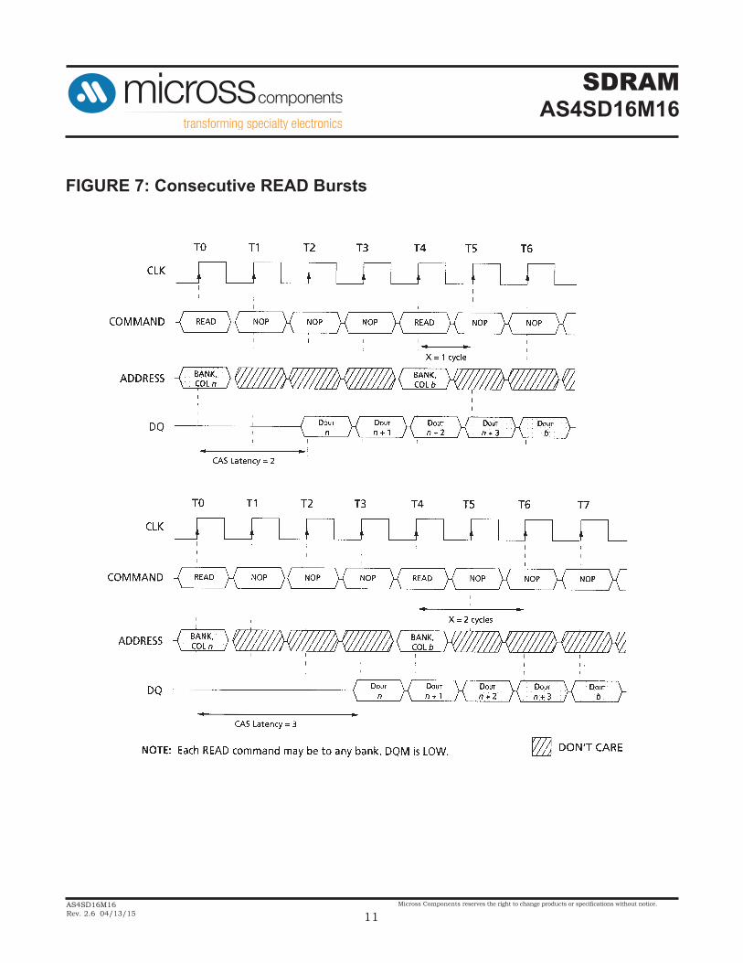
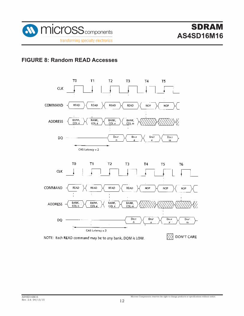
Data from any READ burst may be truncated with a subsequent READ command, and data from a fixed-length READ burst may be immediately followed by data from a READ command. In either case, a continuous flow of data can be maintained. The first data element from the new burst follows either the last element of a complete burst or the last desired data element of a longer burst that is being truncated. The new READ command should be issued x cycles before the clock edge at which the last desired data element is valid, where x equals the CAS latency minus one. This is shown in Figure 7 for CAS latencies of two and three; data element n+3 is either the last of a burst of four or the last desired of a longer burst. The 256MB SDRAM uses a pipelined architecture and therefore does not require the 2n rule associated with a prefetch architecture. A READ command can be initiated on any clock cycle following a previous READ command. Full-speed ran-dom read accesses can be performed to the same bank, as shown in Figure 8, or each subsequent READ may be performed to different bank.
FIGURE 5: READ Command FIGURE 6: CAS Latency
SDRAMAS4SD16M16
AS4SD16M16Rev. 2.6 04/13/15
Micross Components reserves the right to change products or specifications without notice.
11
FIGURE 7: Consecutive READ Bursts
SDRAMAS4SD16M16
AS4SD16M16Rev. 2.6 04/13/15
Micross Components reserves the right to change products or specifications without notice.
12
FIGURE 8: Random READ Accesses
SDRAMAS4SD16M16
AS4SD16M16Rev. 2.6 04/13/15
Micross Components reserves the right to change products or specifications without notice.
13
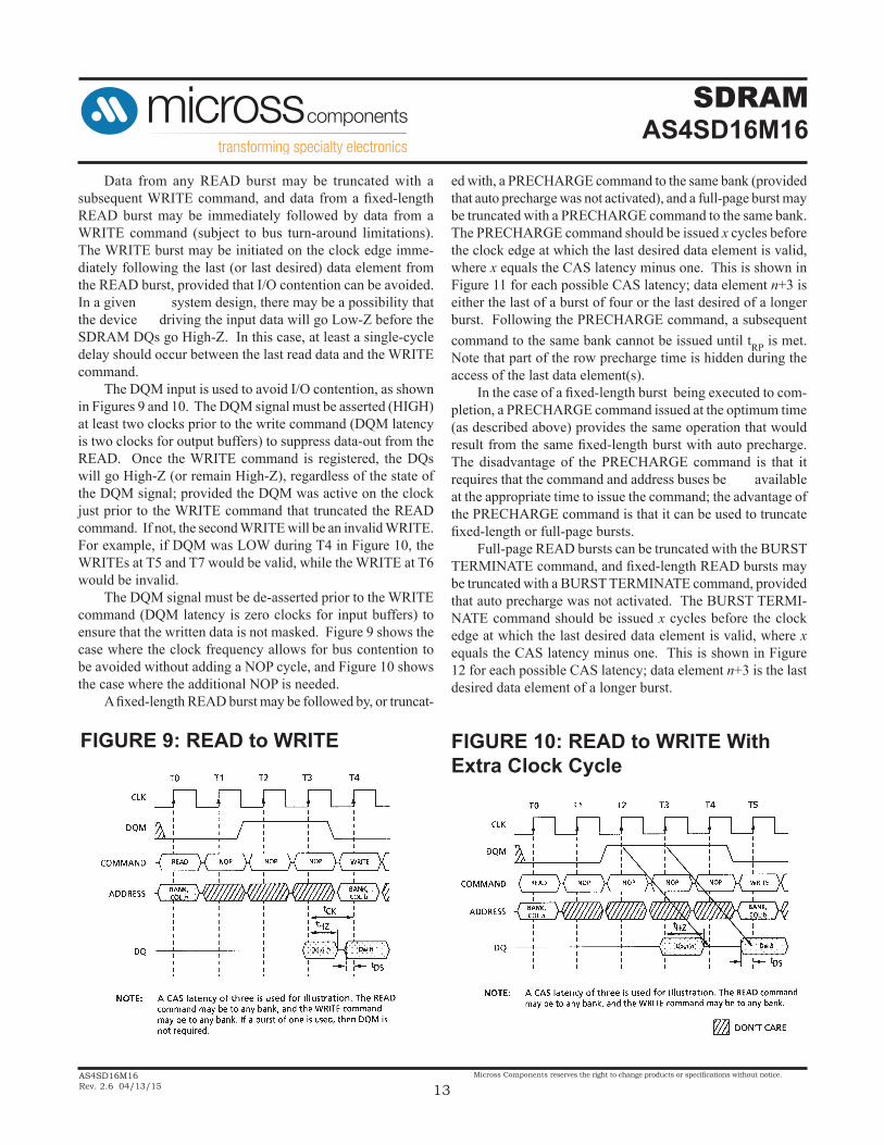
Data from any READ burst may be truncated with a subsequent WRITE command, and data from a fixed-length READ burst may be immediately followed by data from a WRITE command (subject to bus turn-around limitations). The WRITE burst may be initiated on the clock edge imme-diately following the last (or last desired) data element from the READ burst, provided that I/O contention can be avoided. In a given system design, there may be a possibility that the device driving the input data will go Low-Z before the SDRAM DQs go High-Z. In this case, at least a single-cycle delay should occur between the last read data and the WRITE command. The DQM input is used to avoid I/O contention, as shown in Figures 9 and 10. The DQM signal must be asserted (HIGH) at least two clocks prior to the write command (DQM latency is two clocks for output buffers) to suppress data-out from the READ. Once the WRITE command is registered, the DQs will go High-Z (or remain High-Z), regardless of the state of the DQM signal; provided the DQM was active on the clock just prior to the WRITE command that truncated the READ command. If not, the second WRITE will be an invalid WRITE. For example, if DQM was LOW during T4 in Figure 10, the WRITEs at T5 and T7 would be valid, while the WRITE at T6 would be invalid. The DQM signal must be de-asserted prior to the WRITE command (DQM latency is zero clocks for input buffers) to ensure that the written data is not masked. Figure 9 shows the case where the clock frequency allows for bus contention to be avoided without adding a NOP cycle, and Figure 10 shows the case where the additional NOP is needed. A fixed-length READ burst may be followed by, or truncat-
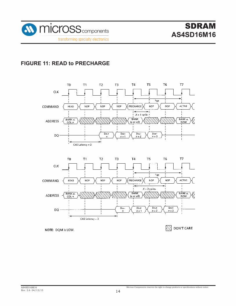
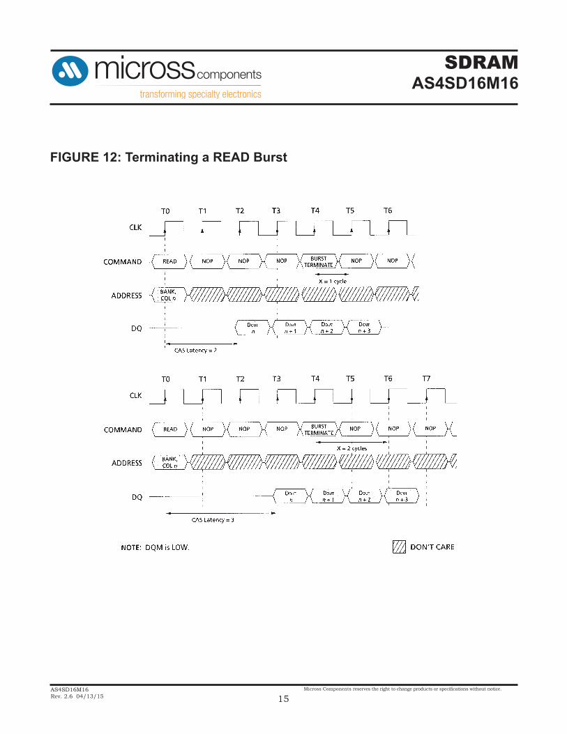
ed with, a PRECHARGE command to the same bank (provided that auto precharge was not activated), and a full-page burst may be truncated with a PRECHARGE command to the same bank. The PRECHARGE command should be issued x cycles before the clock edge at which the last desired data element is valid, where x equals the CAS latency minus one. This is shown in Figure 11 for each possible CAS latency; data element n+3 is either the last of a burst of four or the last desired of a longer burst. Following the PRECHARGE command, a subsequent command to the same bank cannot be issued until tRP is met. Note that part of the row precharge time is hidden during the access of the last data element(s). In the case of a fixed-length burst being executed to com-pletion, a PRECHARGE command issued at the optimum time (as described above) provides the same operation that would result from the same fixed-length burst with auto precharge. The disadvantage of the PRECHARGE command is that it requires that the command and address buses be available at the appropriate time to issue the command; the advantage of the PRECHARGE command is that it can be used to truncate fixed-length or full-page bursts. Full-page READ bursts can be truncated with the BURST TERMINATE command, and fixed-length READ bursts may be truncated with a BURST TERMINATE command, provided that auto precharge was not activated. The BURST TERMI-NATE command should be issued x cycles before the clock edge at which the last desired data element is valid, where x equals the CAS latency minus one. This is shown in Figure 12 for each possible CAS latency; data element n+3 is the last desired data element of a longer burst.
FIGURE 9: READ to WRITE FIGURE 10: READ to WRITE With Extra Clock Cycle
SDRAMAS4SD16M16
AS4SD16M16Rev. 2.6 04/13/15
Micross Components reserves the right to change products or specifications without notice.
14
FIGURE 11: READ to PRECHARGE
SDRAMAS4SD16M16
AS4SD16M16Rev. 2.6 04/13/15
Micross Components reserves the right to change products or specifications without notice.
15
FIGURE 12: Terminating a READ Burst
SDRAMAS4SD16M16
AS4SD16M16Rev. 2.6 04/13/15
Micross Components reserves the right to change products or specifications without notice.
16
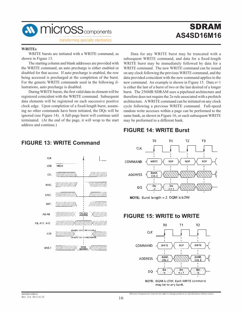
WRITEs WRITE bursts are initiated with a WRITE command, as shown in Figure 13. The starting column and blank addresses are provided with the WRITE command, an auto precharge is either enabled or disabled for that access. If auto precharge is enabled, the row being accessed is precharged at the completion of the burst. For the generic WRITE commands used in the following il-lustrations, auto precharge is disabled. During WRITE bursts, the first valid data-in element will be registered coincident with the WRITE command. Subsequent data elements will be registered on each successive positive clock edge. Upon completion of a fixed-length burst, assum-ing no other commands have been initiated, the DQs will be ignored (see Figure 14). A full-page burst will continue until terminated. (At the end of the page, it will wrap to the start address and continue.)
Data for any WRITE burst may be truncated with a subsequent WRITE command, and data for a fixed-length WRITE burst may be immediately followed by data for a WRITE command. The new WRITE command can be issued on any clock following the previous WRITE command, and the data provided coincident with the new command applies to the new command. An example is shown in Figure 15. Data n+1 is either the last of a burst of two or the last desired of a longer burst. The 256MB SDRAM uses a pipelined architecture and therefore does not require the 2n rule associated with a prefetch architecture. A WRITE command can be initiated on any clock cycle following a previous WRITE command. Full-speed random write accesses within a page can be performed to the same bank, as shown in Figure 16, or each subsequent WRITE may be preformed to a different bank.
FIGURE 13: WRITE Command
FIGURE 14: WRITE Burst
FIGURE 15: WRITE to WRITE
SDRAMAS4SD16M16
AS4SD16M16Rev. 2.6 04/13/15
Micross Components reserves the right to change products or specifications without notice.
17
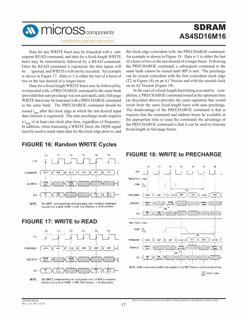
Data for any WRITE burst may be truncated with a sub-sequent READ command, and data for a fixed-length WRITE burst may be immediately followed by a READ command. Once the READ command is registered, the data inputs will be ignored, and WRITEs will not be executed. An example is shown in Figure 17. Data n+1 is either the last of a burst of two or the last desired of a longer burst. Data for a fixed-length WRITE burst may be followed by, or truncated with, a PRECHARGE command to the same bank (provided that auto precharge was not activated), and a full-page WRITE burst may be truncated with a PRECHARGE command to the same bank. The PRECHARGE command should be issued tWR after the clock edge at which the last desired input data element is registered. The auto precharge mode requires a tWR of at least one clock plus time, regardless of frequency. In addition, when truncating a WRITE burst, the DQM signal must be used to mask input data for the clock edge prior to, and
the clock edge coincident with, the PRECHARGE command. An example is shown in Figure 18. Data n+1 is either the last of a burst of two or the last desired of a longer burst. Following the PRECHARGE command, a subsequent command to the same bank cannot be issued until tRP is met. The precharge can be issued coincident with the first coincident clock edge (T2 in Figure 18) on an A1 Version and with the second clock on an A2 Version (Figure 18). In the case of a fixed-length burst being executed to com-pletion, a PRECHARGE command issued at the optimum time (as described above) provides the same operation that would result from the same fixed-length burst with auto precharge. The disadvantage of the PRECHARGE command is that is requires that the command and address buses be available at the appropriate time to issue the command; the advantage of the PRECHARGE command is that it can be used to truncate fixed-length or full-page bursts.
FIGURE 16: Random WRITE Cycles
FIGURE 17: WRITE to READ
FIGURE 18: WRITE to PRECHARGE
SDRAMAS4SD16M16
AS4SD16M16Rev. 2.6 04/13/15
Micross Components reserves the right to change products or specifications without notice.
18
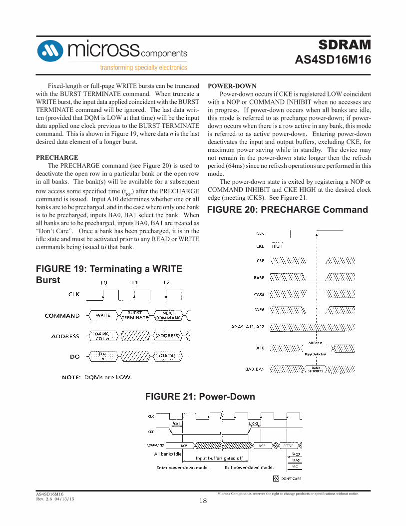
Fixed-length or full-page WRITE bursts can be truncated with the BURST TERMINATE command. When truncate a WRITE burst, the input data applied coincident with the BURST TERMINATE command will be ignored. The last data writ-ten (provided that DQM is LOW at that time) will be the input data applied one clock previous to the BURST TERMINATE command. This is shown in Figure 19, where data n is the last desired data element of a longer burst.
PRECHARGE The PRECHARGE command (see Figure 20) is used to deactivate the open row in a particular bank or the open row in all banks. The bank(s) will be available for a subsequent row access some specified time (tRP) after the PRECHARGE command is issued. Input A10 determines whether one or all banks are to be precharged, and in the case where only one bank is to be precharged, inputs BA0, BA1 select the bank. When all banks are to be precharged, inputs BA0, BA1 are treated as “Don’t Care”. Once a bank has been precharged, it is in the idle state and must be activated prior to any READ or WRITE commands being issued to that bank.
POWER-DOWN Power-down occurs if CKE is registered LOW coincident with a NOP or COMMAND INHIBIT when no accesses are in progress. If power-down occurs when all banks are idle, this mode is referred to as precharge power-down; if power-down occurs when there is a row active in any bank, this mode is referred to as active power-down. Entering power-down deactivates the input and output buffers, excluding CKE, for maximum power saving while in standby. The device may not remain in the power-down state longer then the refresh period (64ms) since no refresh operations are performed in this mode. The power-down state is exited by registering a NOP or COMMAND INHIBIT and CKE HIGH at the desired clock edge (meeting tCKS). See Figure 21.
FIGURE 20: PRECHARGE Command
FIGURE 19: Terminating a WRITE Burst
FIGURE 21: Power-Down
SDRAMAS4SD16M16
AS4SD16M16Rev. 2.6 04/13/15
Micross Components reserves the right to change products or specifications without notice.
19
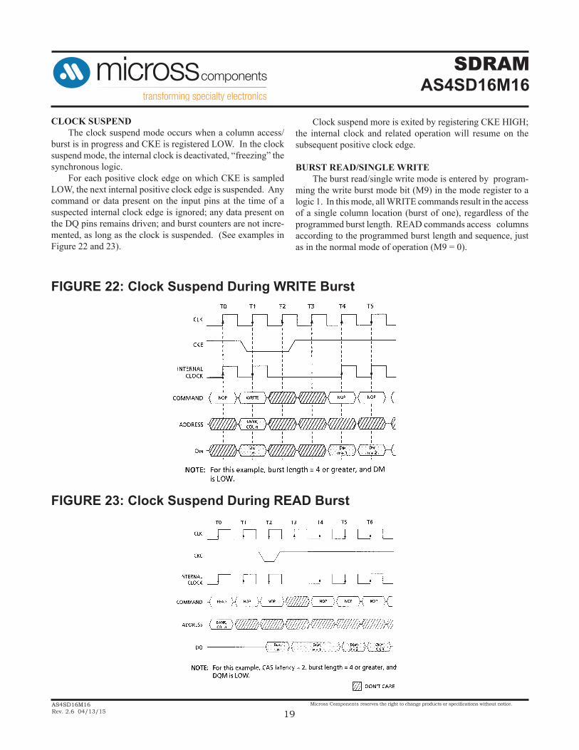
CLOCK SUSPEND The clock suspend mode occurs when a column access/burst is in progress and CKE is registered LOW. In the clock suspend mode, the internal clock is deactivated, “freezing” the synchronous logic. For each positive clock edge on which CKE is sampled LOW, the next internal positive clock edge is suspended. Any command or data present on the input pins at the time of a suspected internal clock edge is ignored; any data present on the DQ pins remains driven; and burst counters are not incre-mented, as long as the clock is suspended. (See examples in Figure 22 and 23).
Clock suspend more is exited by registering CKE HIGH; the internal clock and related operation will resume on the subsequent positive clock edge.
BURST READ/SINGLE WRITE The burst read/single write mode is entered by program-ming the write burst mode bit (M9) in the mode register to a logic 1. In this mode, all WRITE commands result in the access of a single column location (burst of one), regardless of the programmed burst length. READ commands access columns according to the programmed burst length and sequence, just as in the normal mode of operation (M9 = 0).
FIGURE 22: Clock Suspend During WRITE Burst
FIGURE 23: Clock Suspend During READ Burst
SDRAMAS4SD16M16
AS4SD16M16Rev. 2.6 04/13/15
Micross Components reserves the right to change products or specifications without notice.
20
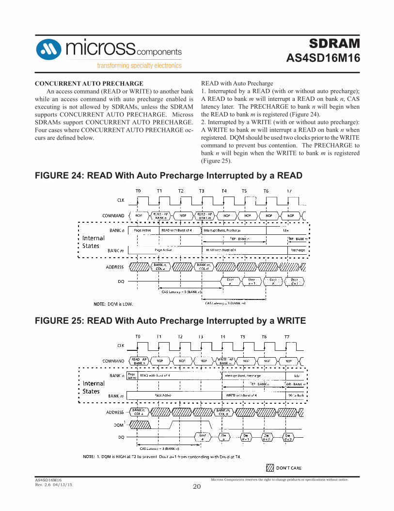
CONCURRENT AUTO PRECHARGE An access command (READ or WRITE) to another bank while an access command with auto precharge enabled is executing is not allowed by SDRAMs, unless the SDRAM supports CONCURRENT AUTO PRECHARGE. Micross SDRAMs support CONCURRENT AUTO PRECHARGE. Four cases where CONCURRENT AUTO PRECHARGE oc-curs are defined below.
READ with Auto Precharge1. Interrupted by a READ (with or without auto precharge); A READ to bank m will interrupt a READ on bank n, CAS latency later. The PRECHARGE to bank n will begin when the READ to bank m is registered (Figure 24).2. Interrupted by a WRITE (with or without auto precharge): A WRITE to bank m will interrupt a READ on bank n when registered. DQM should be used two clocks prior to the WRITE command to prevent bus contention. The PRECHARGE to bank n will begin when the WRITE to bank m is registered (Figure 25).
FIGURE 24: READ With Auto Precharge Interrupted by a READ
FIGURE 25: READ With Auto Precharge Interrupted by a WRITE
SDRAMAS4SD16M16
AS4SD16M16Rev. 2.6 04/13/15
Micross Components reserves the right to change products or specifications without notice.
21
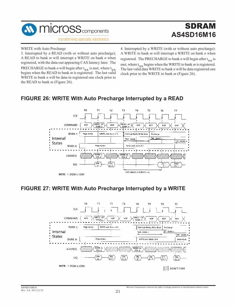
WRITE with Auto Precharge3. Interrupted by a READ (with or without auto precharge); A READ to bank m will interrupt a WRITE on bank n when registered, with the data-out appearing CAS latency later. The PRECHARGE to bank n will begin after tWR is met, where tWR begins when the READ to bank m is registered. The last valid WRITE to bank n will be data-in registered one clock prior to the READ to bank m (Figure 26).
4. Interrupted by a WRITE (with or without auto precharge): A WRITE to bank m will interrupt a WRITE on bank n when registered. The PRECHARGE to bank n will begin after tWR is met, where tWR begins when the WRITE to bank m is registered. The last valid data WRITE to bank n will be data registered one clock prior to the WRITE to bank m (Figure 26).
FIGURE 26: WRITE With Auto Precharge Interrupted by a READ
FIGURE 27: WRITE With Auto Precharge Interrupted by a WRITE
SDRAMAS4SD16M16
AS4SD16M16Rev. 2.6 04/13/15
Micross Components reserves the right to change products or specifications without notice.
22
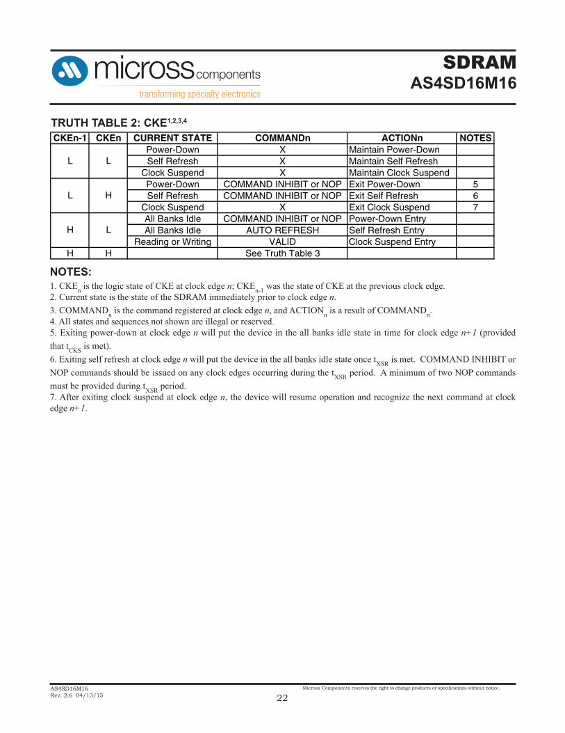
TRUTH TABLE 2: CKE1,2,3,4
CKEn-1 CKEn CURRENT STATE COMMANDn ACTIONn NOTESPower-Down X Maintain Power-DownSelf Refresh X Maintain Self Refresh
Clock Suspend X Maintain Clock SuspendPower-Down COMMAND INHIBIT or NOP Exit Power-Down 5Self Refresh COMMAND INHIBIT or NOP Exit Self Refresh 6
Clock Suspend X Exit Clock Suspend 7All Banks Idle COMMAND INHIBIT or NOP Power-Down EntryAll Banks Idle AUTO REFRESH Self Refresh Entry
Reading or Writing VALID Clock Suspend EntryH H See Truth Table 3
L
L
H
H
L
L
NOTES:1. CKEn is the logic state of CKE at clock edge n; CKEn-1 was the state of CKE at the previous clock edge.2. Current state is the state of the SDRAM immediately prior to clock edge n.3. COMMANDn is the command registered at clock edge n, and ACTIONn is a result of COMMANDn.4. All states and sequences not shown are illegal or reserved.5. Exiting power-down at clock edge n will put the device in the all banks idle state in time for clock edge n+1 (provided that tCKS is met).6. Exiting self refresh at clock edge n will put the device in the all banks idle state once tXSR is met. COMMAND INHIBIT or NOP commands should be issued on any clock edges occurring during the tXSR period. A minimum of two NOP commands must be provided during tXSR period.7. After exiting clock suspend at clock edge n, the device will resume operation and recognize the next command at clock edge n+1.
SDRAMAS4SD16M16
AS4SD16M16Rev. 2.6 04/13/15
Micross Components reserves the right to change products or specifications without notice.
23
NOTES:1. This table applies when CKEn-1 was HIGH and CKEn is HIGH (see Truth Table 2) and after tXSR has been met (if the previ-ous state was self refresh).2. This table is bank-specific, except where noted, i.e., the current state is for a specific bank and the commands shown are those allowed to be issued to that bank when in that state. Exceptions are covered in the notes below.3. Current state definitions: Idle: The bank has been precharged, and tRP has been met. Row Active: A row in the bank has been activated, and tRCD has been met. No data bursts/accesses and no register accesses are in progress. Read: A READ burst has been initiated, with auto precharge disabled, and has not yet terminated or been terminated. Write: A WRITE burst has been initiated, with auto precharge disabled, and has not yet terminated or been terminated.4. The following states must not be interrupted by a command issued to the same bank. COMMAND INHIBIT or NOP com-mands, or allowable commands to the other bank should be issued on any clock edge occurring during these states. Allowable commands to the other bank are determined by its current state and Truth Table 3, and according to Truth Table 4. Precharging: Starts with registration of a PRECHARGE command and ends when tRP is met. Once tRP is met, the bank will be in the idle state. Row Activating: Starts with registration of an ACTIVE command and ends when tRCD is met. Once tRCD is met, the bank will be in the row active state. Read w/ Auto Precharge Enabled: Starts with registration of a READ command with auto precharge enabled and ends when tRP has been met. Once tRP is met, the bank will be in the idle state. Write w/ Auto Precharge Enabled: Starts with registration of a WRITE command with auto precharge enabled and ends when tRP has been met. Once tRP is met, the bank will be in the idle state. (continued on next page)
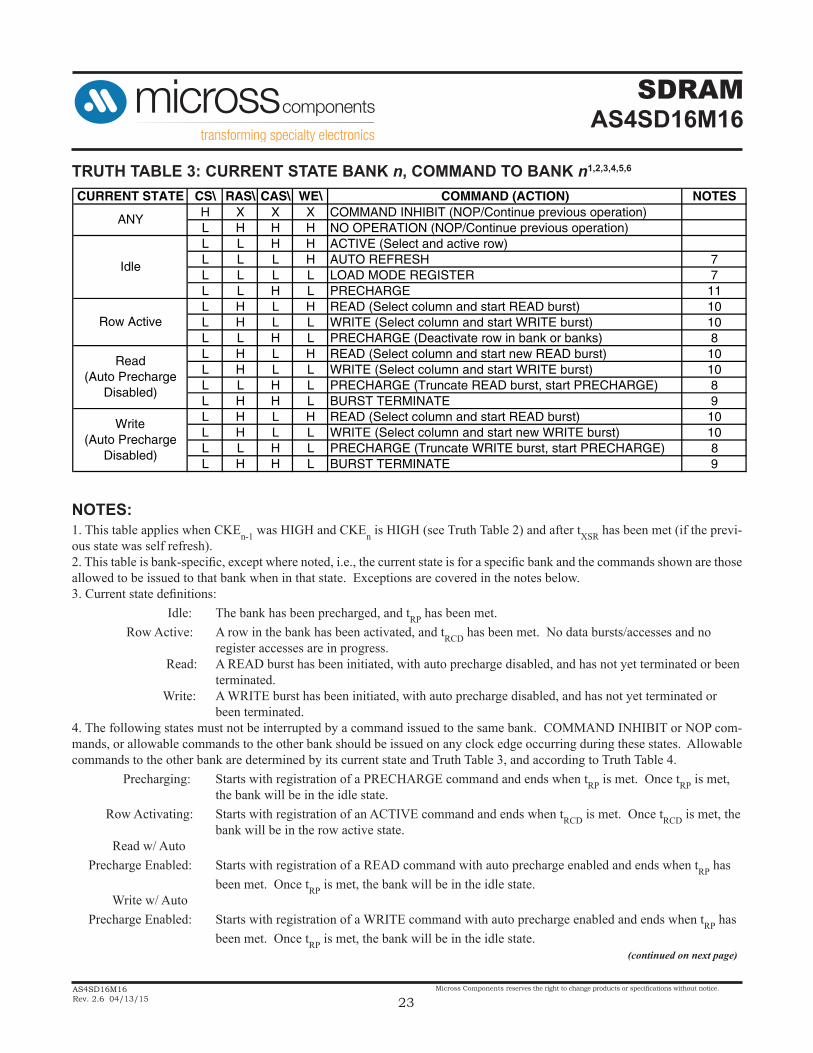
TRUTH TABLE 3: CURRENT STATE BANK n, COMMAND TO BANK n1,2,3,4,5,6
CURRENT STATE CS\ RAS\ CAS\ WE\ COMMAND (ACTION) NOTESH X X X COMMAND INHIBIT (NOP/Continue previous operation)L H H H NO OPERATION (NOP/Continue previous operation)L L H H ACTIVE (Select and active row)L L L H AUTO REFRESH 7L L L L LOAD MODE REGISTER 7L L H L PRECHARGE 11L H L H READ (Select column and start READ burst) 10L H L L WRITE (Select column and start WRITE burst) 10L L H L PRECHARGE (Deactivate row in bank or banks) 8L H L H READ (Select column and start new READ burst) 10L H L L WRITE (Select column and start WRITE burst) 10L L H L PRECHARGE (Truncate READ burst, start PRECHARGE) 8L H H L BURST TERMINATE 9L H L H READ (Select column and start READ burst) 10L H L L WRITE (Select column and start new WRITE burst) 10L L H L PRECHARGE (Truncate WRITE burst, start PRECHARGE) 8L H H L BURST TERMINATE 9
Write (Auto Precharge
Disabled)
ANY
Idle
Row Active
Read (Auto Precharge
Disabled)
SDRAMAS4SD16M16
AS4SD16M16Rev. 2.6 04/13/15
Micross Components reserves the right to change products or specifications without notice.
24
NOTES (continued):5. The following states must not be interrupted by any executable command; COMMAND INHIBIT or NOP commands must be applied on each positive clock edge during these states. Refreshing: Starts with registration of an AUTO REFRESH command and ends when tRC is met. Once tRC is met, the SDRAM will be in the all banks idle state. Accessing Mode Register: Starts with registration of a LOAD MODE REGISTER command and ends when tMRD has been met. Once tMRD is met, the SDRAM will be in the all banks idle state. Precharging All: States with registration of a PRECHARGE ALL command and ends when tRP is met. Once tRP is met, all banks will be in the idle state.6. All states and sequences not shown are illegal or reserved.7. Not bank-specific; requires that all banks are idle.8. May or may not be bank-specific; if all banks are to be precharged, all must be in valid state for precharging.9. Not bank-specific; BURST TERMINATE affects the most recent READ or WRITE burst, regardless of bank.10. READs or WRITEs listed in the Command column include READs or WRITEs with auto precharge enabled and READs or WRITEs with auto precharge disabled.11. Does not affect the state of the bank and acts as a NOP to that bank.
SDRAMAS4SD16M16
AS4SD16M16Rev. 2.6 04/13/15
Micross Components reserves the right to change products or specifications without notice.
25
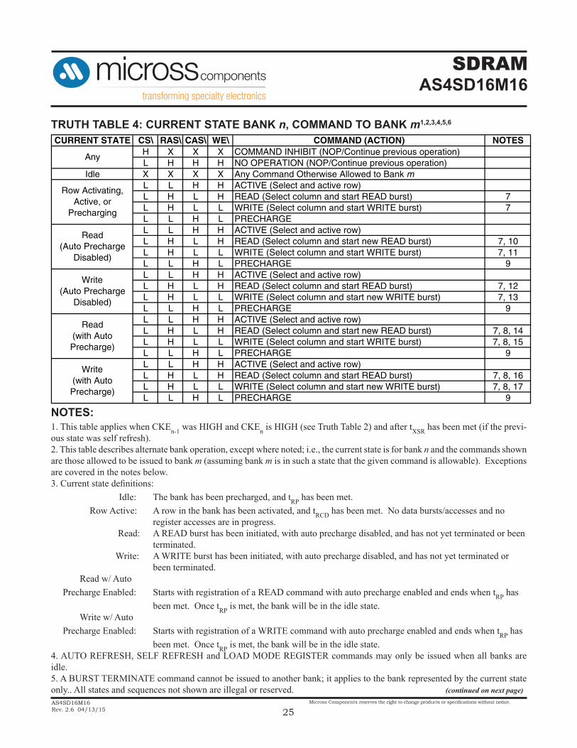
TRUTH TABLE 4: CURRENT STATE BANK n, COMMAND TO BANK m1,2,3,4,5,6
CURRENT STATE CS\ RAS\ CAS\ WE\ COMMAND (ACTION) NOTESH X X X COMMAND INHIBIT (NOP/Continue previous operation)L H H H NO OPERATION (NOP/Continue previous operation)
Idle X X X X Any Command Otherwise Allowed to Bank mL L H H ACTIVE (Select and active row)L H L H READ (Select column and start READ burst) 7L H L L WRITE (Select column and start WRITE burst) 7L L H L PRECHARGEL L H H ACTIVE (Select and active row)L H L H READ (Select column and start new READ burst) 7, 10L H L L WRITE (Select column and start WRITE burst) 7, 11L L H L PRECHARGE 9L L H H ACTIVE (Select and active row)L H L H READ (Select column and start READ burst) 7, 12L H L L WRITE (Select column and start new WRITE burst) 7, 13L L H L PRECHARGE 9L L H H ACTIVE (Select and active row)L H L H READ (Select column and start new READ burst) 7, 8, 14L H L L WRITE (Select column and start WRITE burst) 7, 8, 15L L H L PRECHARGE 9L L H H ACTIVE (Select and active row)L H L H READ (Select column and start READ burst) 7, 8, 16L H L L WRITE (Select column and start new WRITE burst) 7, 8, 17L L H L PRECHARGE 9
Write (Auto Precharge
Disabled)
Row Activating, Active, or
Precharging
Read (with Auto Precharge)
Write (with Auto Precharge)
Any
Read (Auto Precharge
Disabled)
NOTES:1. This table applies when CKEn-1 was HIGH and CKEn is HIGH (see Truth Table 2) and after tXSR has been met (if the previ-ous state was self refresh).2. This table describes alternate bank operation, except where noted; i.e., the current state is for bank n and the commands shown are those allowed to be issued to bank m (assuming bank m is in such a state that the given command is allowable). Exceptions are covered in the notes below.3. Current state definitions: Idle: The bank has been precharged, and tRP has been met. Row Active: A row in the bank has been activated, and tRCD has been met. No data bursts/accesses and no register accesses are in progress. Read: A READ burst has been initiated, with auto precharge disabled, and has not yet terminated or been terminated. Write: A WRITE burst has been initiated, with auto precharge disabled, and has not yet terminated or been terminated. Read w/ Auto Precharge Enabled: Starts with registration of a READ command with auto precharge enabled and ends when tRP has been met. Once tRP is met, the bank will be in the idle state. Write w/ Auto Precharge Enabled: Starts with registration of a WRITE command with auto precharge enabled and ends when tRP has been met. Once tRP is met, the bank will be in the idle state.4. AUTO REFRESH, SELF REFRESH and LOAD MODE REGISTER commands may only be issued when all banks are idle.5. A BURST TERMINATE command cannot be issued to another bank; it applies to the bank represented by the current state only.. All states and sequences not shown are illegal or reserved. (continued on next page)
SDRAMAS4SD16M16
AS4SD16M16Rev. 2.6 04/13/15
Micross Components reserves the right to change products or specifications without notice.
26
NOTES (continued):5. A BURST TERMINATE command cannot be issued to another bank; it applies to the bank represented by the current state only.6. All states and sequences not shown are illegal or reserved.7. READs or WRITEs to bank m listed in the Command column include READs or WRITEs with auto precharge enabled and READs or WRITEs with auto precharge disabled.8. CONCURRENT AUTO PRECHARGE: bank n will initiate the auto precharge command when its burst has been interrupted by bank m’s burst.9. Burst in bank n continues as initiated.10. For a READ without auto precharge interrupted by a READ (with or without auto precharge), the READ to bank m will interrupt the READ on bank n, CAS latency later (Figure 7).11. For a READ without auto precharge interrupted by a WRITE (with or without auto precharge), the WRITE to bank m will interrupt the READ on bank n when registered (Figures 9 and 10). DQM should be used one clock prior to the WRITE com-mand to prevent bus contention.12. For a WRITE without auto precharge interrupted by a READ (with or without auto precharge), the READ to bank m will interrupt the WRITE on bank n when registered (Figure 17), with the data-out appearing CAS latency later. The last valid WRITE to bank n will be data-in registered one clock prior to the READ on bank m.13. For a WRITE without auto precharge interrupted by a WRITE (with or without auto precharge), the WRITE to bank m will interrupt the WRITE on bank n when registered (Figure 15). The last valid WRITE to bank n will be data-in registered one clock prior to the READ to bank m.14. For a READ with auto precharge interrupted by a READ (with or without auto precharge), the READ to bank m will inter-rupt the READ on bank n, CAS latency later. The PRECHARGE to bank n will begin when the READ to bank m is registered (Figure 25).15. For a READ with auto precharge interrupted by a WRITE (with or without auto precharge), the WRITE to bank m will interrupt the READ on bank n when registered. DQM should be used two clocks prior to the WRITE command to prevent bus contention. The PRECHARGE to bank n will begin when the WRITE to bank m is registered (Figure 25). 16. For a WRITE with auto precharge interrupted by a READ (with or without auto precharge), the READ to bank m will interrupt the WRITE on bank n when registered, with the data-out appearing CAS latency later. The PRECHARGE to bank n will begin after tWR is met, where tWR begins when the READ to bank m is registered. The last valid WRITE to bank n will be data-in registered one clock prior to the READ to bank m (Figure 26).17. For a WRITE with auto precharge interrupted by a WRITE (with or without auto precharge), the WRITE to bank m will interrupt the WRITE on bank n when registered. The PRECHARGE to bank n will begin after tWR is met, where tWR begins when the WRITE to bank m is registered. The last valid WRITE to bank n will be data registered one clock prior to the WRITE to bank m (Figure 27).
SDRAMAS4SD16M16
AS4SD16M16Rev. 2.6 04/13/15
Micross Components reserves the right to change products or specifications without notice.
27
*Stresses greater than those listed under “Absolute Maximum Ratings” may cause permanent damage to the device. This is a stress rating only and functional operation of the device at these or any other conditions above those indicated in the operation section of this specification is not implied. Exposure to absolute maximum rating conditions for extended periods may affect reliability.**Junction temperature depends upon package type, cycle time, loading, ambient temperature and airflow, and humidity (plastics).
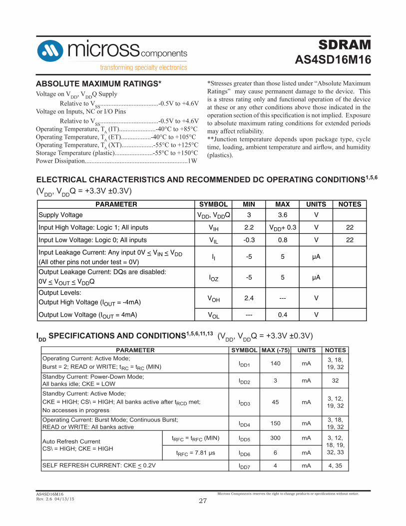
ABSOLUTE MAXIMUM RATINGS*Voltage on VDD, VDDQ Supply Relative to VSS...................................-0.5V to +4.6VVoltage on Inputs, NC or I/O Pins Relative to VSS...................................-0.5V to +4.6VOperating Temperature, TA (IT)......................-40°C to +85°COperating Temperature, TA (ET)..................-40°C to +105°COperating Temperature, TA (XT)...................-55°C to +125°CStorage Temperature (plastic).......................-55°C to +150°CPower Dissipation..............................................................1W
ELECTRICAL CHARACTERISTICS AND RECOMMENDED DC OPERATING CONDITIONS1,5,6
(VDD, VDDQ = +3.3V ±0.3V)PARAMETER SYMBOL MIN MAX UNITS NOTES
Supply Voltage VDD, VDDQ 3 3.6 V
Input High Voltage: Logic 1; All inputs VIH 2.2 VDD+ 0.3 V 22
Input Low Voltage: Logic 0; All inputs VIL -0.3 0.8 V 22
Input Leakage Current: Any input 0V < VIN < VDD
(All other pins not under test = 0V)II -5 5 µA
Output Leakage Current: DQs are disabled: 0V < VOUT < VDDQ
IOZ -5 5 µA
Output Levels: Output High Voltage (IOUT = -4mA)
VOH 2.4 --- V
Output Low Voltage (IOUT = 4mA) VOL --- 0.4 V
IDD SPECIFICATIONS AND CONDITIONS1,5,6,11,13 (VDD, VDDQ = +3.3V ±0.3V)
SYMBOL MAX (-75) UNITS NOTES
IDD1 140 mA 3, 18, 19, 32
IDD2 3 mA 32
IDD3 45 mA 3, 12, 19, 32
IDD4 150 mA 3, 18, 19, 32
tRFC = tRFC (MIN) IDD5 300 mA
tRFC = 7.81 µs IDD6 6 mA
IDD7 4 mA 4, 35SELF REFRESH CURRENT: CKE < 0.2V
Operating Current: Burst Mode; Continuous Burst;READ or WRITE: All banks active
Auto Refresh CurrentCS\ = HIGH; CKE = HIGH
3, 12, 18, 19, 32, 33
PARAMETEROperating Current: Active Mode;Burst = 2; READ or WRITE; tRC = tRC (MIN)
Standby Current: Power-Down Mode;All banks idle; CKE = LOWStandby Current: Active Mode;CKE = HIGH; CS\ = HIGH; All banks active after tRCD met;No accesses in progress
SDRAMAS4SD16M16
AS4SD16M16Rev. 2.6 04/13/15
Micross Components reserves the right to change products or specifications without notice.
28
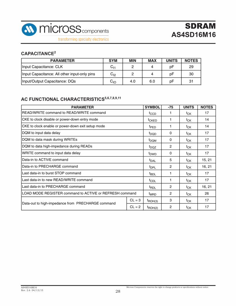
CAPACITANCE2
PARAMETER SYM MIN MAX UNITS NOTES
Input Capacitance: CLK CI1 2 4 pF 29
Input Capacitance: All other input-only pins CI2 2 4 pF 30
Input/Output Capacitance: DQs CIO 4.0 6.0 pF 31
AC FUNCTIONAL CHARACTERISTICS5,6,7,8,9,11
SYMBOL -75 UNITS NOTES
tCCD 1 tCK 17
tCKED 1 tCK 14
tPED 1 tCK 14
tDQD 0 tCK 17
tDQM 0 tCK 17
tDQZ 2 tCK 17
tDWD 0 tCK 17
tDAL 5 tCK 15, 21
tDPL 2 tCK 16, 21
tBDL 1 tCK 17
tCDL 1 tCK 17
tRDL 2 tCK 16, 21
tMRD 2 tCK 26
CL = 3 tROH(3) 3 tCK 17
CL = 2 tROH(2) 2 tCK 17
PARAMETER
LOAD MODE REGISTER command to ACTIVE or REFRESH command
Data-out to high-impedance from PRECHARGE command
DQM to input data delay
CKE to clock enable or power-down exit setup mode
CKE to clock disable or power-down entry mode
READ/WRITE command to READ/WRITE command
DQM to data high-impedance during READs
WRITE command to input data delay
Data-in to ACTIVE command
DQM to data mask during WRITEs
Last data-in to PRECHARGE command
Last data-in to new READ/WRITE command
Last data-in to burst STOP command
Data-in to PRECHARGE command
SDRAMAS4SD16M16
AS4SD16M16Rev. 2.6 04/13/15
Micross Components reserves the right to change products or specifications without notice.
29
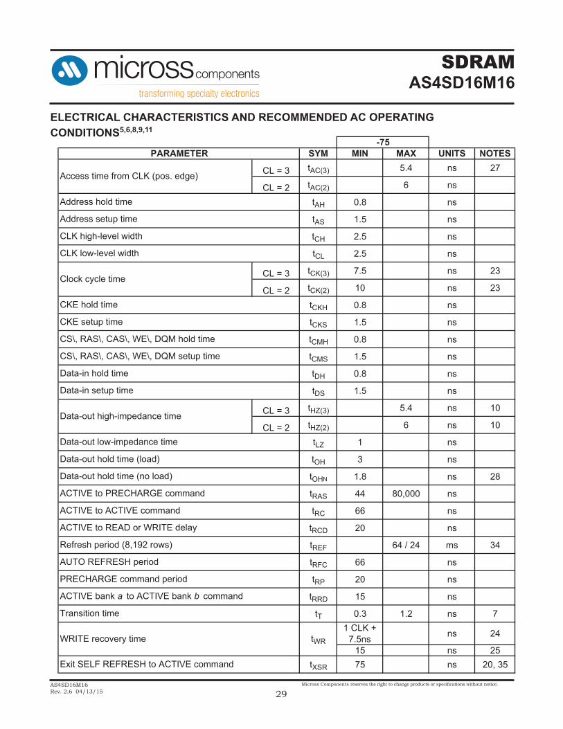
SYM MIN MAX UNITS NOTES
CL = 3 tAC(3) 5.4 ns 27
CL = 2 tAC(2) 6 ns
tAH 0.8 ns
tAS 1.5 ns
tCH 2.5 ns
tCL 2.5 ns
CL = 3 tCK(3) 7.5 ns 23
CL = 2 tCK(2) 10 ns 23
tCKH 0.8 ns
tCKS 1.5 ns
tCMH 0.8 ns
tCMS 1.5 ns
tDH 0.8 ns
tDS 1.5 ns
CL = 3 tHZ(3) 5.4 ns 10
CL = 2 tHZ(2) 6 ns 10
tLZ 1 ns
tOH 3 ns
tOHN 1.8 ns 28
tRAS 44 80,000 ns
tRC 66 ns
tRCD 20 ns
tREF 64 / 24 ms 34
tRFC 66 ns
tRP 20 ns
tRRD 15 ns
tT 0.3 1.2 ns 71 CLK +
7.5ns ns 24
15 ns 25tXSR 75 ns 20, 35
-75
Access time from CLK (pos. edge)
Clock cycle time
Data-out high-impedance time
CS\, RAS\, CAS\, WE\, DQM setup time
CS\, RAS\, CAS\, WE\, DQM hold time
CKE setup time
CKE hold time
Address hold time
Address setup time
tWR
PARAMETER
WRITE recovery time
AUTO REFRESH period
ACTIVE to READ or WRITE delay
Refresh period (8,192 rows)
ACTIVE to ACTIVE command
ACTIVE to PRECHARGE command
Data-out hold time (no load)
CLK high-level width
Exit SELF REFRESH to ACTIVE command
Transition time
ACTIVE bank a to ACTIVE bank b command
PRECHARGE command period
CLK low-level width
Data-out hold time (load)
Data-out low-impedance time
Data-in setup time
Data-in hold time
ELECTRICAL CHARACTERISTICS AND RECOMMENDED AC OPERATING CONDITIONS5,6,8,9,11
SDRAMAS4SD16M16
AS4SD16M16Rev. 2.6 04/13/15
Micross Components reserves the right to change products or specifications without notice.
30
NOTES:1. All voltages referenced to VSS.2. This parameter is sampled. VDD, VDDQ = +3.3V; f = 1 MHz, TA = 25°C; pin under test biased at 1.4V.3. IDD is dependent on output loading and cycle rates. Speci-fied values are obtained with minimum cycle time and the outputs open.4. Enables on-chip refresh and address counters.5. The minimum specifications are used only to indicate cycle time at which proper operation over the full temperature range is ensured: (0°C < TA < +125°C for XT), (-40°C < TA < +85°C for IT), and (-45°C < TA < +105°C for ET).6. An initial pause of 100µs is required after power-up, followed by two AUTO REFRESH commands, before proper device operation is ensured. (VDD and VDDQ must be powered up si-multaneously. VSS and VSSQ must be at the same potential.) The two AUTO REFRESH command wake-ups should be repeated any time the tREF refresh requirement is exceeded.7. AC characteristics assume tT = 1ns.8. In addition to meeting the transition rate specification, the clock and CKE must transit between VIH and VIL (or between VIL and VIH) in a monotonic manner.9. Outputs measured at 1.5V with equivalent load:
10. tHZ defines the time at which the output achieves the open circuit condition; it is not a reference to VOH or VOL. The last valid data element will meet tOH before going High-Z.11. AC operating and IDD test conditions have VIL = 0V and VIH = 3.0V using a measurement reference level of 1.5V. If the input transition time is longer than 1ns, then the timing is measured from VIL (MAX) and VIH (MIN) and no longer from the 1.5V mid-point.12. Other input signals are allowed to transition no more than once every two clocks and are otherwise at valid VIH or VIL levels.13. IDD specifications are tested after the device is properly initialized.14. Timing actually specified by tCKS; clock(s) specified as a reference only at minimum cycle rate.15. Timing actually specified by tWR plus tRP; clock(s) specified as a reference only at minimum cycle rate.16. Timing actually specified by tWR.17. Required clocks are specified by JEDEC functionality and are not dependent on any timing parameter.
18. The IDD current will increase or decrease proportionally according to the amount of frequency alteration for the test condition.19. Address transitions average one transition every two clocks.20. CLK must be toggled a minimum of two times during this period.21. Based on tCK = 7.5ns for -75.22. VIH overshoot: VIL (MAX) = VDDQ = 2V for a pulse width < 3ns, and the pulse width cannot be greater than one third of the cycle rate. VIL undershoot: VIL (MIN) = -2V for a pulse width < 3ns.23. The clock frequency must remain constant (stable clock is defined as a signal cycling within timing constraints specified for the clock pin) during access or precharge states (READ, WRITE, including tWR, and PRECHARGE commands). CKE may be used to reduce the data rate.24. Auto precharge mode only. The precharge timing budget (tRP) begins 7.5ns after the first clock delay, after the last WRITE is executed. May not exceed limit set for precharge mode.25. Precharge mode only.26. JEDEC and PC100 specify three clock.27. for -75 at CL = 3 with no load is 4.6ns and is guaranteed by design.28. Parameter guaranteed by design.29. PC100 specifies a maximum of 4pF.30. PC100 specifies a maximum of 5pF.31. PC100 specifies a maximum of 6.5pF.32. CL = 3 and tCK = 7.5ns.33. CKE is HIGH during refresh command period tRFC (MIN) else CKE is LOW. The IDD6 limit is actually a nominal value and does not result in a fail value.34. 64ms refresh for IT, ET temperature options, 24ms refresh for XT temperature option.35. Self refresh mode available for IT and ET only.
SDRAMSDRAMSDRAMSDRAMSDRAMAS4SD16M16
AS4SD16M16Rev. 1.7 3/2/09
Austin Semiconductor, Inc. reserves the right to change products or specifications without notice.
30
Austin Semiconductor, Inc.
NOTES:1. All voltages referenced to V
SS.
2. This parameter is sampled. VDD
, VDD
Q = +3.3V; f = 1 MHz, TA
= 25°C; pin under test biased at 1.4V.3. I
DD is dependent on output loading and cycle rates. Speci-
fied values are obtained with minimum cycle time and the out-puts open.4. Enables on-chip refresh and address counters.5. The minimum specifications are used only to indicate cycletime at which proper operation over the full temperature rangeis ensured: (0°C < T
A < +125°C for XT), (-40°C < T
A < +85°C
for IT), and (-45°C < TA < +105°C for IT+).
6. An initial pause of 100µs is required after power-up, followedby two AUTO REFRESH commands, before proper device op-eration is ensured. (V
DD and V
DDQ must be powered up simul-
taneously. VSS
and VSS
Q must be at the same potential.) Thetwo AUTO REFRESH command wake-ups should be repeatedany time the tREF refresh requirement is exceeded.7. AC characteristics assume t
T = 1ns.
8. In addition to meeting the transition rate specification, theclock and CKE must transit between V
IH and V
IL (or between V
IL
and VIH
) in a monotonic manner.9. Outputs measured at 1.5V with equivalent load:
10. tHZ
defines the time at which the output achieves the opencircuit condition; it is not a reference to V
OH or V
OL. The last
valid data element will meet tOH
before going High-Z.11. AC operating and I
DD test conditions have V
IL = 0V and V
IH
= 3.0V using a measurement reference level of 1.5V. If the inputtransition time is longer than 1ns, then the timing is measuredfrom V
IL (MAX) and V
IH (MIN) and no longer from the 1.5V
mid-point.12. Other input signals are allowed to transition no more thanonce every two clocks and are otherwise at valid V
IH or V
IL
levels.13. I
DD specifications are tested after the device is properly ini-
tialized.14. Timing actually specified by t
CKS; clock(s) specified as a
reference only at minimum cycle rate.15. Timing actually specified by t
WR plus t
RP; clock(s) specified
as a reference only at minimum cycle rate.16. Timing actually specified by t
WR.
17. Required clocks are specified by JEDEC functionality andare not dependent on any timing parameter.
18. The IDD
current will increase or decrease proportionally ac-cording to the amount of frequency alteration for the test con-dition.19. Address transitions average one transition every two clocks.20. CLK must be toggled a minimum of two times during thisperiod.21. Based on t
CK = 7.5ns for -75.
22. VIH
overshoot: VIL
(MAX) = VDD
Q = 2V for a pulse width <3ns, and the pulse width cannot be greater than one third of thecycle rate. V
IL undershoot: V
IL (MIN) = -2V for a pulse width <
3ns.23. The clock frequency must remain constant (stable clock isdefined as a signal cycling within timing constraints specifiedfor the clock pin) during access or precharge states (READ,WRITE, including t
WR, and PRECHARGE commands). CKE
may be used to reduce the data rate.24. Auto precharge mode only. The precharge timing budget(t
RP) begins 7.5ns after the first clock delay, after the last WRITE
is executed. May not exceed limit set for precharge mode.25. Precharge mode only.26. JEDEC and PC100 specify three clock.27. for -75 at CL = 3 with no load is 4.6ns and is guaranteed bydesign.28. Parameter guaranteed by design.29. PC100 specifies a maximum of 4pF.30. PC100 specifies a maximum of 5pF.31. PC100 specifies a maximum of 6.5pF.32. CL = 3 and tCK = 7.5ns.33. CKE is HIGH during refresh command period t
RFC (MIN) else
CKE is LOW. The IDD
6 limit is actually a nominal value anddoes not result in a fail value.34. 64ms refresh for IT, IT+ temperature options, 24ms refreshfor XT temperature option.35. Self refresh mode available for IT and IT+ only.
SDRAMAS4SD16M16
AS4SD16M16Rev. 2.6 04/13/15
Micross Components reserves the right to change products or specifications without notice.
31
INITIALIZE AND LOAD MODE REGISTER2
TIMING PARAMETERS
MIN MAX MIN MAX
tAH 0.8 ns tCKS 1.5 ns
tAS 1.5 ns tCMH 0.8 ns
tCH 2.5 ns tCMS 1.5 ns
tCL 2.5 ns tMRD3 2 tCK
tCK(3) 7.5 ns tRFC 66 ns
tCK(2) 10 ns tRP 20 ns
tCKH 0.8 ns
-75UNITS
-75SYMBOL* UNITS SYMBOL*
*CAS latency indicated in parentheses.
NOTES:1. The mode register may be loaded prior to the AUTO REFRESH cycles if desired.2. If CS is HIGH at clock HIGH time, all commands applied are NOP, with CKE a “Don’t Care”.3. JEDEC and PC100 specify three clocks4. Outputs are guaranteed High-Z after command is issued.5. A12 should be a LOW at tP + 1.
SDRAMAS4SD16M16
AS4SD16M16Rev. 2.6 04/13/15
Micross Components reserves the right to change products or specifications without notice.
32
POWER DOWN MODE1
*CAS latency indicated in parentheses.
NOTES:1. Violating refresh requirements during power-down may result in loss of data.
TIMING PARAMETERS
MIN MAX MIN MAX
tAH 0.8 ns tCK(2) 10 ns
tAS 1.5 ns tCKH 0.8 ns
tCH 2.5 ns tCKS 1.5 ns
tCL 2.5 ns tCMH 0.8 ns
tCK(3) 7 ns tCMS 1.5 ns
-75UNITS
-75SYMBOL* UNITS SYMBOL*
SDRAMAS4SD16M16
AS4SD16M16Rev. 2.6 04/13/15
Micross Components reserves the right to change products or specifications without notice.
33
CLOCK SUSPEND MODE1
*CAS latency indicated in parentheses.
NOTES:1. For this example, the burst length = 2, the CAS latency = 3, and auto precharge is disabled.2. A9, A11 and A12 = “Don’t Care”
TIMING PARAMETERS
MIN MAX MIN MAX
tAC(3) 5.4 ns tCKS 1.5 ns
tAC(2) 6 ns tCMH 0.8 ns
tAH 0.8 ns tCMS 1.5 ns
tAS 1.5 ns tDH 0.8 ns
tCH 2.5 ns tDS 1.5 ns
tCL 2.5 ns tHZ(3) 5.4 ns
tCK(3) 7.5 ns tHZ(2) 6 ns
tCK(2) 10 ns tLZ 1 ns
tCKH 0.8 ns tOH 3 ns
-75UNITS
-75SYMBOL* UNITS SYMBOL*
SDRAMAS4SD16M16
AS4SD16M16Rev. 2.6 04/13/15
Micross Components reserves the right to change products or specifications without notice.
34
AUTO REFRESH MODE
*CAS latency indicated in parentheses.
TIMING PARAMETERS
MIN MAX MIN MAX
tAH 0.8 ns tCKH 0.8 ns
tAS 1.5 ns tCKS 1.5 ns
tCH 2.5 ns tCMH 0.8 ns
tCL 2.5 ns tCMS 1.5 ns
tCK(3) 7.5 ns tRFC 66 ns
tCK(2) 10 ns tRP 20 ns
-75UNITS
-75SYMBOL* UNITS SYMBOL*
SDRAMAS4SD16M16
AS4SD16M16Rev. 2.6 04/13/15
Micross Components reserves the right to change products or specifications without notice.
35
SELF REFRESH MODE (IT & ET Temp options ONLY)
*CAS latency indicated in parentheses.
NOTES:1. No maximum time limit for Self Refresh. tRAS(MAX) applied to non-Self Refresh mode.2. tXSR requires minimum of two clocks regardless of frequency or timing.
TIMING PARAMETERS
MIN MAX MIN MAX
tAH 0.8 ns tCKS 1.5 ns
tAS 1.5 ns tCMH 0.8 ns
tCH 2.5 ns tCMS 1.5 ns
tCL 2.5 ns tRAS 44 80,000 ns
tCK(3) 7.5 ns tRP 20 ns
tCK(2) 10 ns tXSR 75 ns
tCKH 0.8 ns
-75UNITS
-75SYMBOL* UNITS SYMBOL*
SDRAMAS4SD16M16
AS4SD16M16Rev. 2.6 04/13/15
Micross Components reserves the right to change products or specifications without notice.
36
READ - WITHOUT AUTO PRECHARGE1
*CAS latency indicated in parentheses.
NOTES:1. For this example, the burst length = 4, the CAS latency = 2, and the READ burst is followed by a “manual” PRECHARGE.2. A9, A11, and A12 = “Don’t Care”
TIMING PARAMETERS
MIN MAX MIN MAX
tAC(3) 5.4 ns tCMH 0.8 ns
tAC(2) 6 ns tCMS 1.5 ns
tAH 0.8 ns tHZ(3) 5.4 ns
tAS 1.5 ns tHZ(2) 6 ns
tCH 2.5 ns tLZ 1 ns
tCL 2.5 ns tOH 3 ns
tCK(3) 7.5 ns tRAS 44 80,000 ns
tCK(2) 10 ns tRC 66 ns
tCKH 0.8 ns tRCD 20 ns
tCKS 1.5 ns tRP 20 ns
-75UNITS
-75SYMBOL* UNITS SYMBOL*
SDRAMAS4SD16M16
AS4SD16M16Rev. 2.6 04/13/15
Micross Components reserves the right to change products or specifications without notice.
37
READ - WITH AUTO PRECHARGE1
*CAS latency indicated in parentheses.
NOTES:1. For this example, the burst length = 4, the CAS latency = 2, and the READ burst is followed by a “manual” PRECHARGE.2. A9, A11, and A12 = “Don’t Care”
TIMING PARAMETERS
MIN MAX MIN MAX
tAC(3) 5.4 ns tCMH 0.8 ns
tAC(2) 6 ns tCMS 1.5 ns
tAH 0.8 ns tHZ(3) 5.4 ns
tAS 1.5 ns tHZ(2) 6 ns
tCH 2.5 ns tLZ 1 ns
tCL 2.5 ns tOH 3 ns
tCK(3) 7.5 ns tRAS 44 80,000 ns
tCK(2) 10 ns tRC 66 ns
tCKH 0.8 ns tRCD 20 ns
tCKS 1.5 ns tRP 20 ns
-75UNITS
-75SYMBOL* UNITS SYMBOL*
SDRAMAS4SD16M16
AS4SD16M16Rev. 2.6 04/13/15
Micross Components reserves the right to change products or specifications without notice.
38
SINGLE READ - WITHOUT AUTO PRECHARGE1
*CAS latency indicated in parentheses.
NOTES:1. For this example, the burst length = 1, the CAS latency = 2, and the READ burst is followed by a “manual” PRECHARGE.2. A9, A11, and A12 = “Don’t Care”3. PRECHARGE command not allowed else tRAS would be violated.
TIMING PARAMETERS
MIN MAX MIN MAX
tAC(3) 5.4 ns tCMH 0.8 ns
tAC(2) 6 ns tCMS 1.5 ns
tAH 0.8 ns tHZ(3) 5.4 ns
tAS 1.5 ns tHZ(2) 6 ns
tCH 2.5 ns tLZ 1 ns
tCL 2.5 ns tOH 3 ns
tCK(3) 7.5 ns tRAS 44 80,000 ns
tCK(2) 10 ns tRC 66 ns
tCKH 0.8 ns tRCD 20 ns
tCKS 1.5 ns tRP 20 ns
-75UNITS
-75SYMBOL* UNITS SYMBOL*
SDRAMAS4SD16M16
AS4SD16M16Rev. 2.6 04/13/15
Micross Components reserves the right to change products or specifications without notice.
39
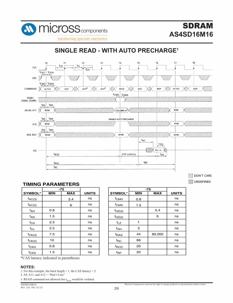
SINGLE READ - WITH AUTO PRECHARGE1
*CAS latency indicated in parentheses.
NOTES:1. For this example, the burst length = 1, the CAS latency = 2.2. A9, A11, and A12 = “Don’t Care”3. READ command not allowed else tRAS would be violated.
TIMING PARAMETERS
MIN MAX MIN MAX
tAC(3) 5.4 ns tCMH 0.8 ns
tAC(2) 6 ns tCMS 1.5 ns
tAH 0.8 ns tHZ(3) 5.4 ns
tAS 1.5 ns tHZ(2) 6 ns
tCH 2.5 ns tLZ 1 ns
tCL 2.5 ns tOH 3 ns
tCK(3) 7.5 ns tRAS 44 80,000 ns
tCK(2) 10 ns tRC 66 ns
tCKH 0.8 ns tRCD 20 ns
tCKS 1.5 ns tRP 20 ns
-75UNITS
-75SYMBOL* UNITS SYMBOL*
SDRAMAS4SD16M16
AS4SD16M16Rev. 2.6 04/13/15
Micross Components reserves the right to change products or specifications without notice.
40
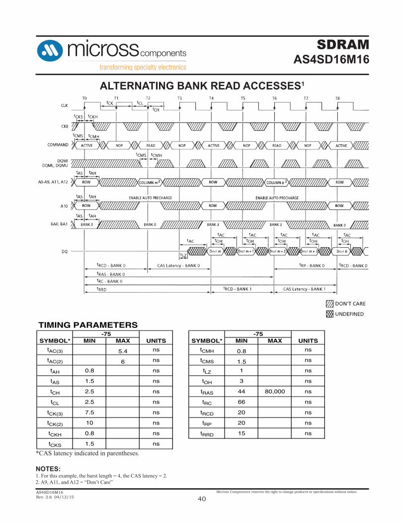
ALTERNATING BANK READ ACCESSES1
*CAS latency indicated in parentheses.
NOTES:1. For this example, the burst length = 4, the CAS latency = 2.2. A9, A11, and A12 = “Don’t Care”
TIMING PARAMETERS
MIN MAX MIN MAX
tAC(3) 5.4 ns tCMH 0.8 ns
tAC(2) 6 ns tCMS 1.5 ns
tAH 0.8 ns tLZ 1 ns
tAS 1.5 ns tOH 3 ns
tCH 2.5 ns tRAS 44 80,000 ns
tCL 2.5 ns tRC 66 ns
tCK(3) 7.5 ns tRCD 20 ns
tCK(2) 10 ns tRP 20 ns
tCKH 0.8 ns tRRD 15 ns
tCKS 1.5 ns
-75UNITS
-75SYMBOL* UNITS SYMBOL*
SDRAMAS4SD16M16
AS4SD16M16Rev. 2.6 04/13/15
Micross Components reserves the right to change products or specifications without notice.
41
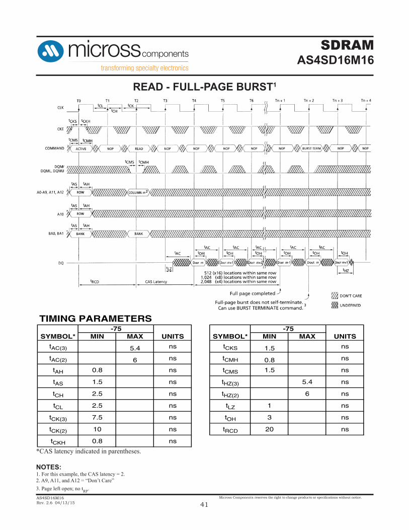
READ - FULL-PAGE BURST1
*CAS latency indicated in parentheses.
NOTES:1. For this example, the CAS latency = 2.2. A9, A11, and A12 = “Don’t Care”3. Page left open; no tRP.
TIMING PARAMETERS
MIN MAX MIN MAX
tAC(3) 5.4 ns tCKS 1.5 ns
tAC(2) 6 ns tCMH 0.8 ns
tAH 0.8 ns tCMS 1.5 ns
tAS 1.5 ns tHZ(3) 5.4 ns
tCH 2.5 ns tHZ(2) 6 ns
tCL 2.5 ns tLZ 1 ns
tCK(3) 7.5 ns tOH 3 ns
tCK(2) 10 ns tRCD 20 ns
tCKH 0.8 ns
-75UNITS
-75SYMBOL* UNITS SYMBOL*
SDRAMAS4SD16M16
AS4SD16M16Rev. 2.6 04/13/15
Micross Components reserves the right to change products or specifications without notice.
42
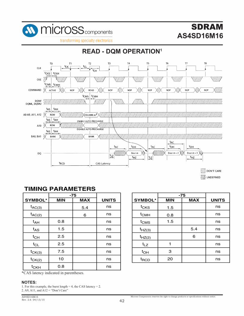
READ - DQM OPERATION1
*CAS latency indicated in parentheses.
NOTES:1. For this example, the burst length = 4, the CAS latency = 2.2. A9, A11, and A12 = “Don’t Care”
TIMING PARAMETERS
MIN MAX MIN MAX
tAC(3) 5.4 ns tCKS 1.5 ns
tAC(2) 6 ns tCMH 0.8 ns
tAH 0.8 ns tCMS 1.5 ns
tAS 1.5 ns tHZ(3) 5.4 ns
tCH 2.5 ns tHZ(2) 6 ns
tCL 2.5 ns tLZ 1 ns
tCK(3) 7.5 ns tOH 3 ns
tCK(2) 10 ns tRCD 20 ns
tCKH 0.8 ns
-75UNITS
-75SYMBOL* UNITS SYMBOL*
SDRAMAS4SD16M16
AS4SD16M16Rev. 2.6 04/13/15
Micross Components reserves the right to change products or specifications without notice.
43
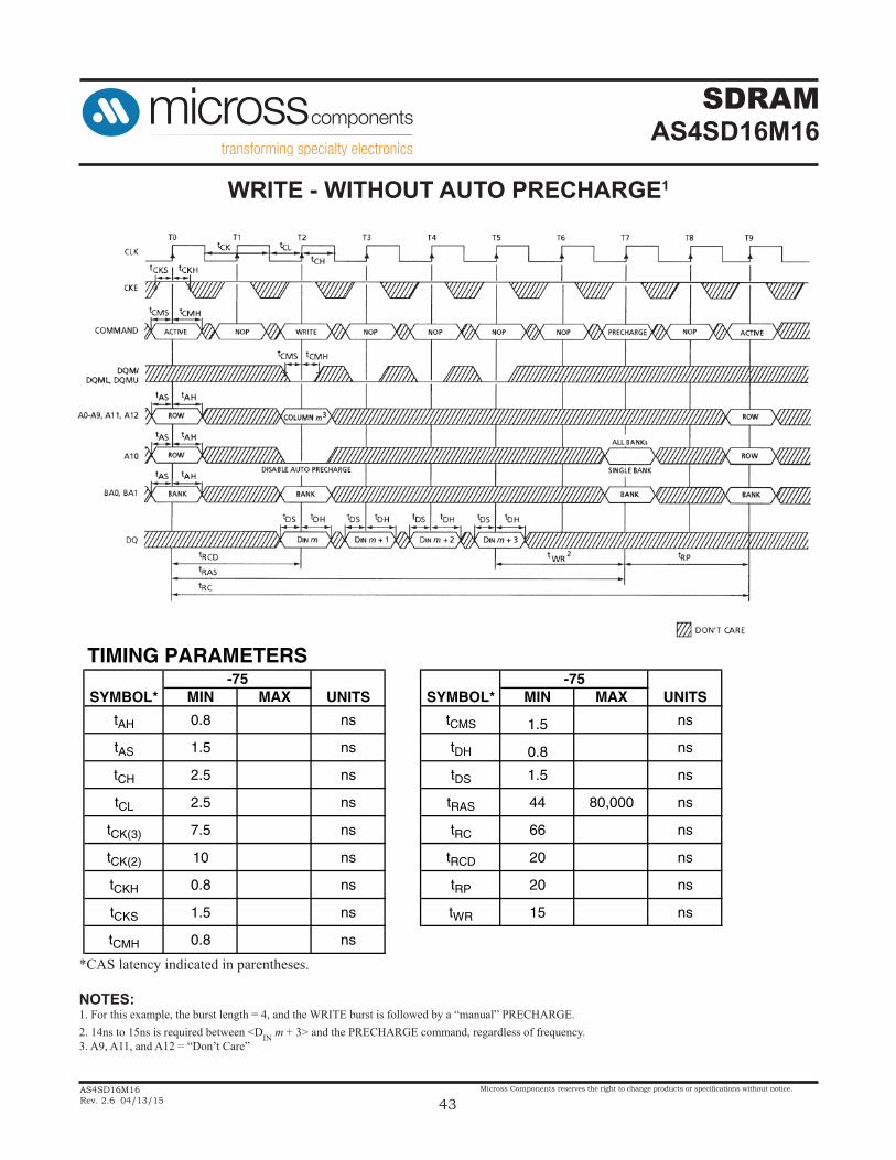
WRITE - WITHOUT AUTO PRECHARGE1
*CAS latency indicated in parentheses.
NOTES:1. For this example, the burst length = 4, and the WRITE burst is followed by a “manual” PRECHARGE.2. 14ns to 15ns is required between <DIN m + 3> and the PRECHARGE command, regardless of frequency.3. A9, A11, and A12 = “Don’t Care”
TIMING PARAMETERS
MIN MAX MIN MAX
tAH 0.8 ns tCMS 1.5 ns
tAS 1.5 ns tDH 0.8 ns
tCH 2.5 ns tDS 1.5 ns
tCL 2.5 ns tRAS 44 80,000 ns
tCK(3) 7.5 ns tRC 66 ns
tCK(2) 10 ns tRCD 20 ns
tCKH 0.8 ns tRP 20 ns
tCKS 1.5 ns tWR 15 ns
tCMH 0.8 ns
-75UNITS
-75SYMBOL* UNITS SYMBOL*
SDRAMAS4SD16M16
AS4SD16M16Rev. 2.6 04/13/15
Micross Components reserves the right to change products or specifications without notice.
44
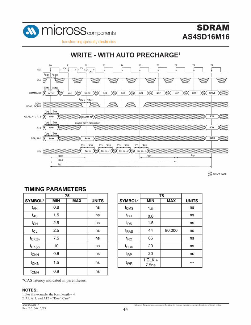
WRITE - WITH AUTO PRECHARGE1
*CAS latency indicated in parentheses.
NOTES:1. For this example, the burst length = 4.2. A9, A11, and A12 = “Don’t Care”
TIMING PARAMETERS
MIN MAX MIN MAX
tAH 0.8 ns tCMS 1.5 ns
tAS 1.5 ns tDH 0.8 ns
tCH 2.5 ns tDS 1.5 ns
tCL 2.5 ns tRAS 44 80,000 ns
tCK(3) 7.5 ns tRC 66 ns
tCK(2) 10 ns tRCD 20 ns
tCKH 0.8 ns tRP 20 ns
tCKS 1.5 ns tWR1 CLK +
7.5ns---
tCMH 0.8 ns
-75UNITS
-75SYMBOL* UNITS SYMBOL*
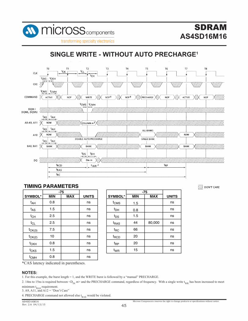
SDRAMAS4SD16M16
AS4SD16M16Rev. 2.6 04/13/15
Micross Components reserves the right to change products or specifications without notice.
45
SINGLE WRITE - WITHOUT AUTO PRECHARGE1
*CAS latency indicated in parentheses.
NOTES:1. For this example, the burst length = 1, and the WRITE burst is followed by a “manual” PRECHARGE.2. 14ns to 15ns is required between <DIN m> and the PRECHARGE command, regardless of frequency. With a single write tWR has been increased to meet minimum tRAS requirement.3. A9, A11, and A12 = “Don’t Care”4. PRECHARGE command not allowed else tRAS would be violated.
TIMING PARAMETERS
MIN MAX MIN MAX
tAH 0.8 ns tCMS 1.5 ns
tAS 1.5 ns tDH 0.8 ns
tCH 2.5 ns tDS 1.5 ns
tCL 2.5 ns tRAS 44 80,000 ns
tCK(3) 7.5 ns tRC 66 ns
tCK(2) 10 ns tRCD 20 ns
tCKH 0.8 ns tRP 20 ns
tCKS 1.5 ns tWR 15 ns
tCMH 0.8 ns
-75UNITS
-75SYMBOL* UNITS SYMBOL*
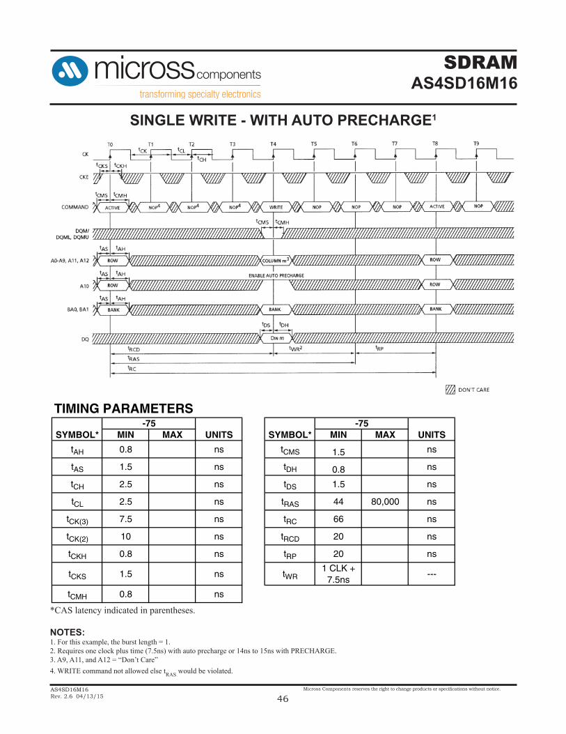
SDRAMAS4SD16M16
AS4SD16M16Rev. 2.6 04/13/15
Micross Components reserves the right to change products or specifications without notice.
46
SINGLE WRITE - WITH AUTO PRECHARGE1
*CAS latency indicated in parentheses.
NOTES:1. For this example, the burst length = 1.2. Requires one clock plus time (7.5ns) with auto precharge or 14ns to 15ns with PRECHARGE.3. A9, A11, and A12 = “Don’t Care”4. WRITE command not allowed else tRAS would be violated.
TIMING PARAMETERS
MIN MAX MIN MAX
tAH 0.8 ns tCMS 1.5 ns
tAS 1.5 ns tDH 0.8 ns
tCH 2.5 ns tDS 1.5 ns
tCL 2.5 ns tRAS 44 80,000 ns
tCK(3) 7.5 ns tRC 66 ns
tCK(2) 10 ns tRCD 20 ns
tCKH 0.8 ns tRP 20 ns
tCKS 1.5 ns tWR1 CLK +
7.5ns---
tCMH 0.8 ns
-75UNITS
-75SYMBOL* UNITS SYMBOL*
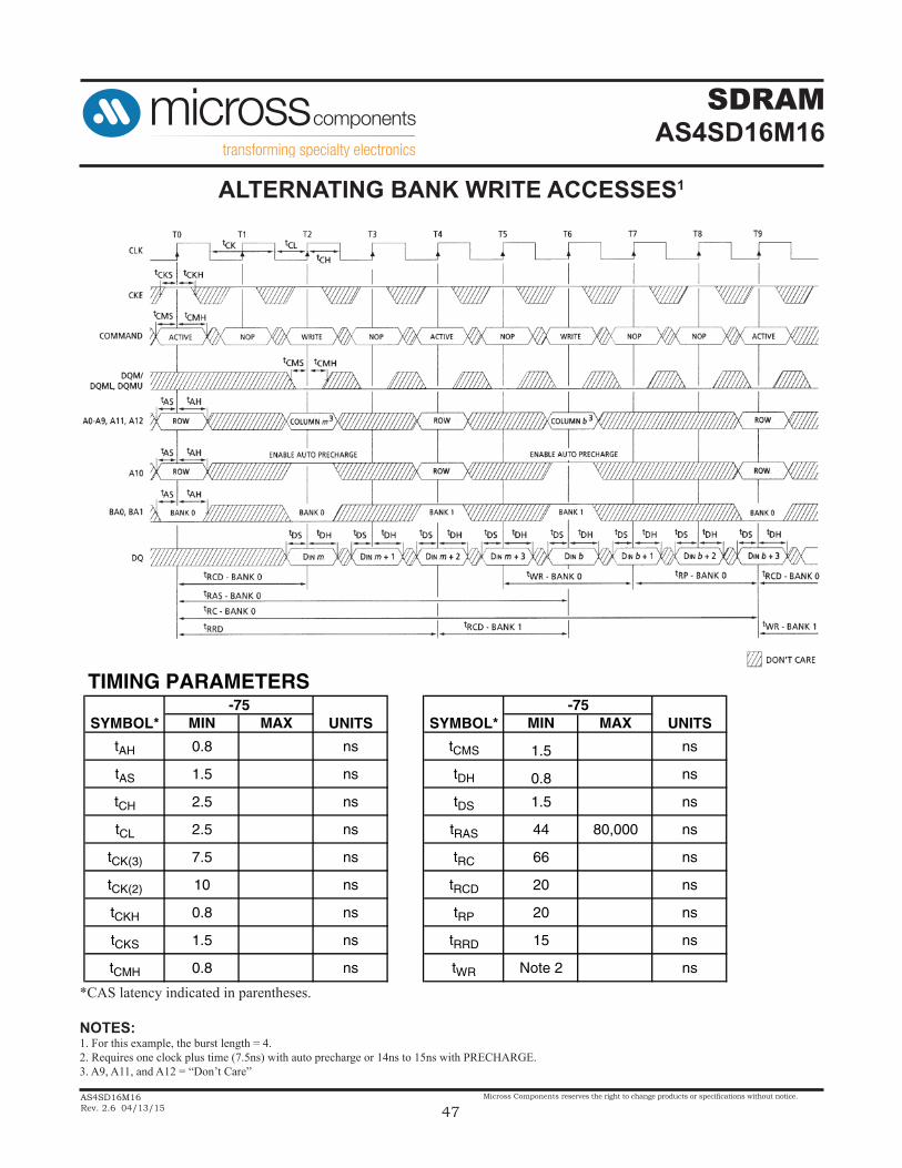
SDRAMAS4SD16M16
AS4SD16M16Rev. 2.6 04/13/15
Micross Components reserves the right to change products or specifications without notice.
47
ALTERNATING BANK WRITE ACCESSES1
*CAS latency indicated in parentheses.
NOTES:1. For this example, the burst length = 4.2. Requires one clock plus time (7.5ns) with auto precharge or 14ns to 15ns with PRECHARGE.3. A9, A11, and A12 = “Don’t Care”
TIMING PARAMETERS
MIN MAX MIN MAX
tAH 0.8 ns tCMS 1.5 ns
tAS 1.5 ns tDH 0.8 ns
tCH 2.5 ns tDS 1.5 ns
tCL 2.5 ns tRAS 44 80,000 ns
tCK(3) 7.5 ns tRC 66 ns
tCK(2) 10 ns tRCD 20 ns
tCKH 0.8 ns tRP 20 ns
tCKS 1.5 ns tRRD 15 ns
tCMH 0.8 ns tWR Note 2 ns
-75UNITS
-75SYMBOL* UNITS SYMBOL*
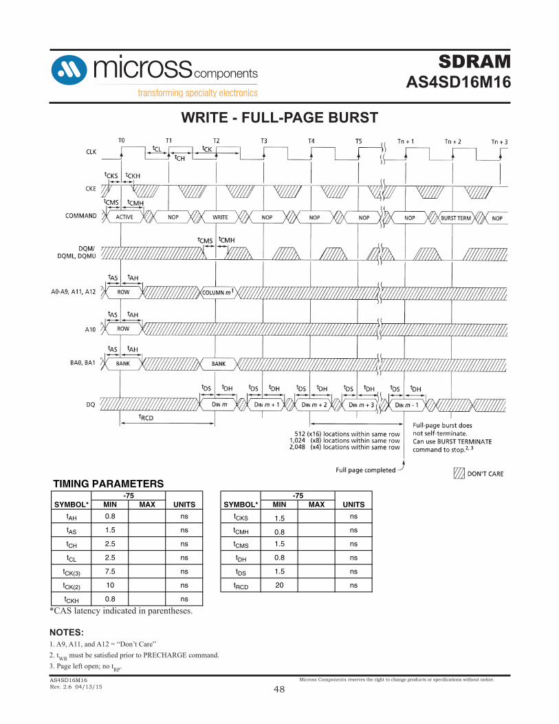
SDRAMAS4SD16M16
AS4SD16M16Rev. 2.6 04/13/15
Micross Components reserves the right to change products or specifications without notice.
48
WRITE - FULL-PAGE BURST
*CAS latency indicated in parentheses.
NOTES:1. A9, A11, and A12 = “Don’t Care”2. tWR must be satisfied prior to PRECHARGE command.3. Page left open; no tRP.
TIMING PARAMETERS
MIN MAX MIN MAX
tAH 0.8 ns tCKS 1.5 ns
tAS 1.5 ns tCMH 0.8 ns
tCH 2.5 ns tCMS 1.5 ns
tCL 2.5 ns tDH 0.8 ns
tCK(3) 7.5 ns tDS 1.5 ns
tCK(2) 10 ns tRCD 20 ns
tCKH 0.8 ns
-75UNITS
-75SYMBOL* UNITS SYMBOL*
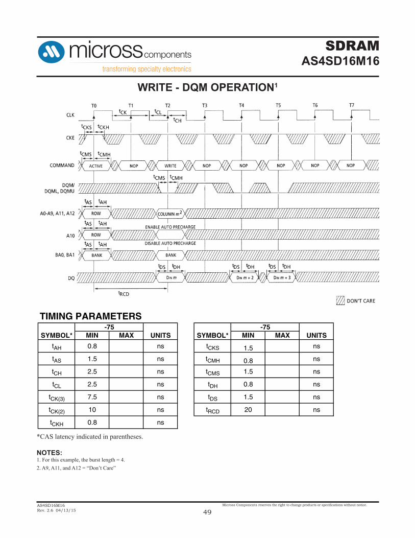
SDRAMAS4SD16M16
AS4SD16M16Rev. 2.6 04/13/15
Micross Components reserves the right to change products or specifications without notice.
49
WRITE - DQM OPERATION1
*CAS latency indicated in parentheses.
NOTES:1. For this example, the burst length = 4.2. A9, A11, and A12 = “Don’t Care”
TIMING PARAMETERS
MIN MAX MIN MAX
tAH 0.8 ns tCKS 1.5 ns
tAS 1.5 ns tCMH 0.8 ns
tCH 2.5 ns tCMS 1.5 ns
tCL 2.5 ns tDH 0.8 ns
tCK(3) 7.5 ns tDS 1.5 ns
tCK(2) 10 ns tRCD 20 ns
tCKH 0.8 ns
-75UNITS
-75SYMBOL* UNITS SYMBOL*
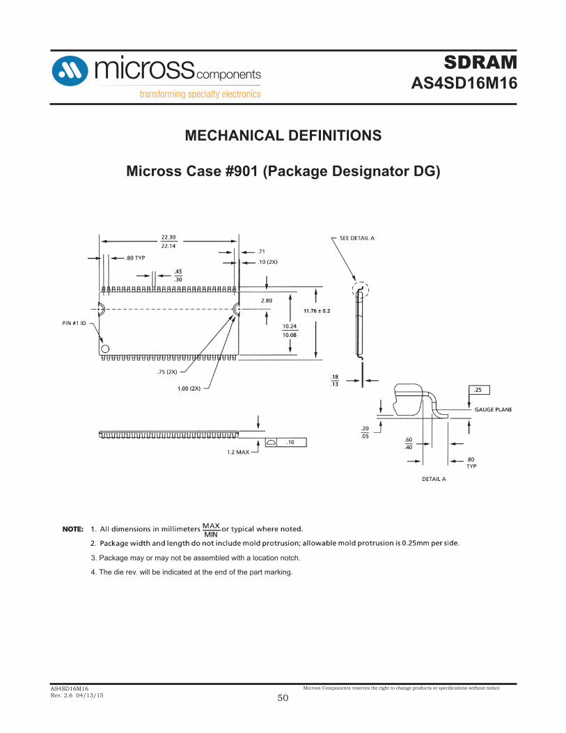
SDRAMAS4SD16M16
AS4SD16M16Rev. 2.6 04/13/15
Micross Components reserves the right to change products or specifications without notice.
50
MECHANICAL DEFINITIONS
Micross Case #901 (Package Designator DG)
3. Package may or may not be assembled with a location notch.
4. The die rev. will be indicated at the end of the part marking.
SDRAMAS4SD16M16
AS4SD16M16Rev. 2.6 04/13/15
Micross Components reserves the right to change products or specifications without notice.
51
ORDERING INFORMATION
*AVAILABLE PROCESSESIT = Industrial Temperature Range -40oC to +85oCET = Enhanced Temperature Range -40°C to +105°CXT = Military Temperature Range -55oC to +125oC
Device Number Package Type Speed Process
AS4SD16M16DG-75/IT 54-pin TSOPII, PbSn plating 133MHz Industrial
AS4SD16M16DG-75/ET 54-pin TSOPII, PbSn plating 133MHz Enhanced
AS4SD16M16DG-75/XT 54-pin TSOPII, PbSn plating 133MHz Military
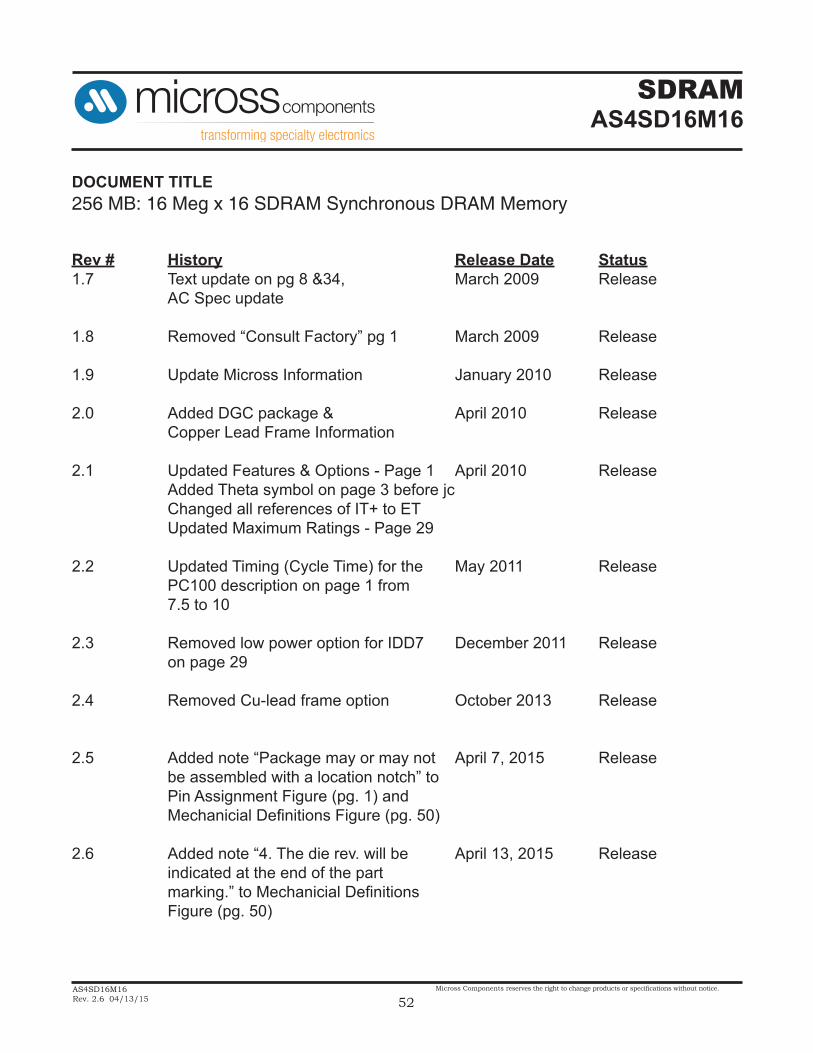
SDRAMAS4SD16M16
AS4SD16M16Rev. 2.6 04/13/15
Micross Components reserves the right to change products or specifications without notice.
52
DOCUMENT TITLE256 MB: 16 Meg x 16 SDRAM Synchronous DRAM Memory
Rev # History Release Date Status1.7 Text update on pg 8 &34, March 2009 Release AC Spec update
1.8 Removed “Consult Factory” pg 1 March 2009 Release
1.9 Update Micross Information January 2010 Release
2.0 Added DGC package & April 2010 Release Copper Lead Frame Information
2.1 Updated Features & Options - Page 1 April 2010 Release Added Theta symbol on page 3 before jc Changed all references of IT+ to ET Updated Maximum Ratings - Page 29
2.2 Updated Timing (Cycle Time) for the May 2011 Release PC100 description on page 1 from 7.5 to 10
2.3 Removed low power option for IDD7 December 2011 Release on page 29
2.4 Removed Cu-lead frame option October 2013 Release
2.5 Added note “Package may or may not April 7, 2015 Release be assembled with a location notch” to Pin Assignment Figure (pg. 1) and MechanicialDefinitionsFigure(pg.50)
2.6 Added note “4. The die rev. will be April 13, 2015 Release indicated at the end of the part marking.”toMechanicialDefinitions Figure (pg. 50)