Embed Size (px)
Citation preview
256MB, 512MB, 1GB (x72, SR, ECC) 240-Pin DDR2 SDRAM UDIMMFeatures
DDR2 SDRAM Unbuffered DIMMMT9HTF3272A – 256MB MT9HTF6472A – 512MBMT9HTF12872A – 1GBFor the latest data sheet, please refer to the Micron® Web site: www.micron.com/products/modules
Features• 240-pin, unbuffered dual in-line memory module
(UDIMM)• Fast data transfer rates: PC2-3200, PC2-4200, or
PC2-5300• 256MB (32 Meg x 72), 512MB (64 Meg x 72)
1GB (128 Meg x 72)• VDD = VDDQ = +1.8V• VDDSPD = +1.7V to +3.6V• JEDEC standard 1.8V I/O (SSTL_18-compatible)• Differential data strobe (DQS, DQS#) option• Four-bit prefetch architecture• DLL to align DQ and DQS transitions with CK• Multiple internal device banks for concurrent
operation• Programmable CAS# latency (CL)• Posted CAS# additive latency (AL)• WRITE latency = READ latency - 1 tCK• Programmable burst lengths: 4 or 8• Adjustable data-output drive strength• 64ms, 8,192-cycle refresh• On-die termination (ODT)• Serial Presence Detect (SPD) with EEPROM• Gold edge contacts• Single rank
Products and specifications discussed herein are
pdf: 09005aef80e6f860, source: 09005aef80e5b799HTF9C32_64_128x72AG_1.fm - Rev. C 6/05 EN 1
Figure 1: 240-Pin DIMM (MO-237 R/C “A”)
Notes: 1. CL = CAS (READ) Latency.2. Not available in 1GB density.
Options Marking• Package
240-pin DIMM (lead-free) Y• Frequency/CAS Latency1
3ns @ CL = 5 (DDR2-667)2 -6673.75ns @ CL = 4 (DDR2-533) -53E5.0ns @ CL = 3 (DDR2-400) -40E
• PCB Height1.18in. (29.97mm)
Height 1.18in. (29.97mm)
subject to change by Micron without notice.
Micron Technology, Inc., reserves the right to change products or specifications without notice.©2003, 2004, 2005 Micron Technology, Inc. All rights reserved.
256MB, 512MB, 1GB (x72, SR, ECC) 240-Pin DDR2 SDRAM UDIMMFeatures
Notes: 1. All part numbers end with a two-place code (not shown), designating component and PCB revisions. Consult factory for current revision codes. Example: MT9HTF6472AY-40EC2.
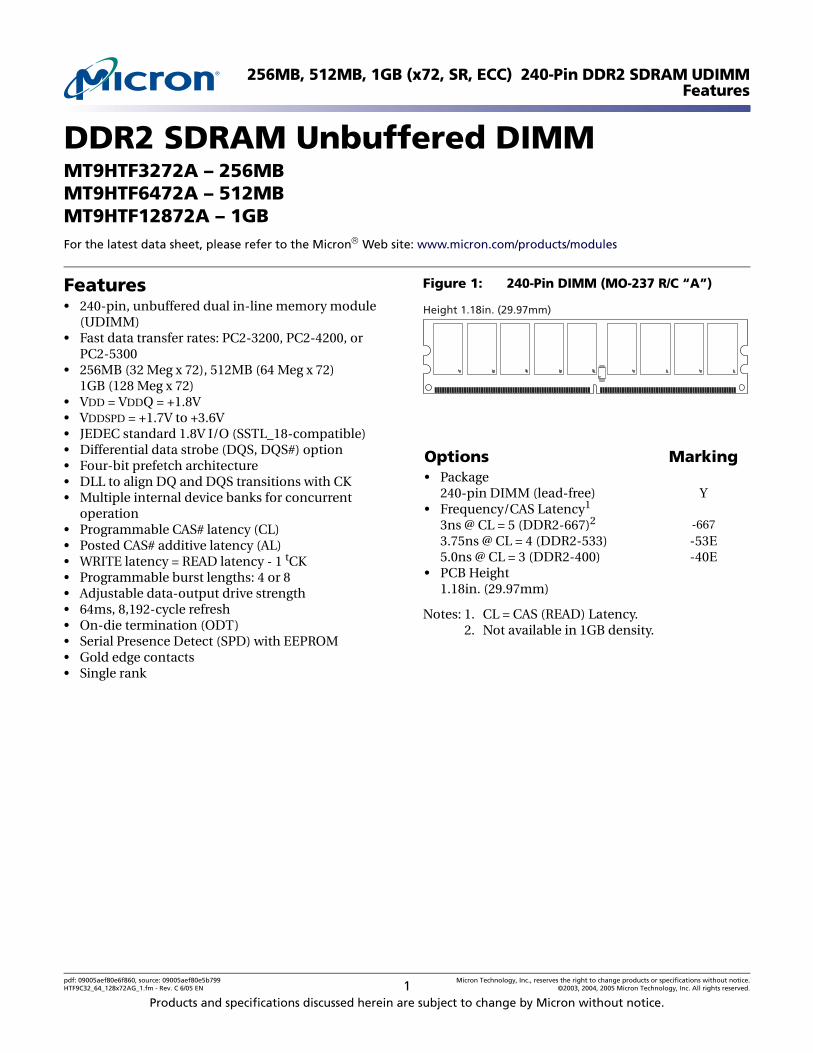
Table 1: Address Table
256MB 512MB 1GB
Refresh Count 8K 8K 8K
Row Addressing 8K (A0–A12) 16K (A0–A13) 16K (A0–A13)
Device Bank Addressing 4 (BA0, BA1) 4 (BA0, BA1) 8 (BA0, BA1, BA2)
Device Page Size per Bank 1KB 1KB 1KB
Device Configuration 256Mb (32 Meg x 8) 512Mb (64 Meg x 8) 1Gb (128 Meg x 8)
Column Addressing 1K (A0–A9) 1K (A0-A9) 1K (A0-A9)
Module Rank Addressing 1 (S0#) 1 (S0#) 1 (S0#)
Table 2: Key Timing Parameters
Speed Grade
Data Rate (MT/s)tRCD(ns)
tRP(ns)
tRC(ns)CL = 3 CL = 4 CL = 5
-667 — 533 667 15 15 55-53E 400 533 — 15 15 55-40E 400 400 — 15 15 55
Table 3: Part Numbers and Timing Parameters
Part Number1Module Densit Configuration
Module Bandwidth
Memory Clock/Data Rate
Latency (CL - tRCD - tRP)
MT9HTF3272AY-667__ 256MB 32 Meg x 72 5.3 GB/s 3.0ns/667 MT/s 5-5-5
MT9HTF3272AY-53E__ 256MB 32 Meg x 72 4.3 GB/s 3.75ns/533 MT/s 4-4-4
MT9HTF3272AY-40E__ 256MB 32 Meg x 72 3.2 GB/s 5.0ns/400 MT/s 3-3-3
MT9HTF6472AY-667__ 512MB 64 Meg x 72 5.3 GB/s 3.0ns/667 MT/s 5-5-5
MT9HTF6472AY-53E__ 512MB 64 Meg x 72 4.3 GB/s 3.75ns/533 MT/s 4-4-4
MT9HTF6472AY-40E__ 512MB 64 Meg x 72 3.2 GB/s 5.0ns/400 MT/s 3-3-3
MT9HTF12872AY-667__ 1GB 128 Meg x 72 5.3 GB/s 3.0ns/667 MT/s 5-5-5
MT9HTF12872AY-53E__ 1GB 128 Meg x 72 4.3 GB/s 3.75ns/533 MT/s 4-4-4
MT9HTF12872AY-40E__ 1GB 128 Meg x 72 3.2 GB/s 5.0ns/400 MT/s 3-3-3
pdf: 09005aef80e6f860, source: 09005aef80e5b799 Micron Technology, Inc., reserves the right to change products or specifications without notice.HTF9C32_64_128x72AG_1.fm - Rev. C 6/05 EN 2 ©2003, 2004, 2005 Micron Technology, Inc. All rights reserved.
pdf: 09005aef80e6f860, source: 09005aef80e5b799 Micron Technology, Inc., reserves the right to change products or specifications without notice.HTF9C32_64_128x72AGTOC.fm - Rev. C 6/05 EN 3 ©2003, 2004, 2005 Micron Technology, Inc. All rights reserved.
256MB, 512MB, 1GB (x72, SR, ECC) 240-Pin DDR2 SDRAM UDIMMTable of Contents
Table of ContentsFeatures . . . . . . . . . . . . . . . . . . . . . . . . . . . . . . . . . . . . . . . . . . . . . . . . . . . . . . . . . . . . . . . . . . . . . . . . . . . . . . . . . . . . . .1Table of Contents . . . . . . . . . . . . . . . . . . . . . . . . . . . . . . . . . . . . . . . . . . . . . . . . . . . . . . . . . . . . . . . . . . . . . . . . . . . . . .3List of Figures . . . . . . . . . . . . . . . . . . . . . . . . . . . . . . . . . . . . . . . . . . . . . . . . . . . . . . . . . . . . . . . . . . . . . . . . . . . . . . . . .4List of Tables . . . . . . . . . . . . . . . . . . . . . . . . . . . . . . . . . . . . . . . . . . . . . . . . . . . . . . . . . . . . . . . . . . . . . . . . . . . . . . . . . .5Pin Assignments and Descriptions. . . . . . . . . . . . . . . . . . . . . . . . . . . . . . . . . . . . . . . . . . . . . . . . . . . . . . . . . . . . . . .6Functional Block Diagram . . . . . . . . . . . . . . . . . . . . . . . . . . . . . . . . . . . . . . . . . . . . . . . . . . . . . . . . . . . . . . . . . . . . . .9General Description. . . . . . . . . . . . . . . . . . . . . . . . . . . . . . . . . . . . . . . . . . . . . . . . . . . . . . . . . . . . . . . . . . . . . . . . . . .10Serial Presence-Detect Operation . . . . . . . . . . . . . . . . . . . . . . . . . . . . . . . . . . . . . . . . . . . . . . . . . . . . . . . . . . . . . .10Initialization . . . . . . . . . . . . . . . . . . . . . . . . . . . . . . . . . . . . . . . . . . . . . . . . . . . . . . . . . . . . . . . . . . . . . . . . . . . . . . . . .11Mode Register (MR) . . . . . . . . . . . . . . . . . . . . . . . . . . . . . . . . . . . . . . . . . . . . . . . . . . . . . . . . . . . . . . . . . . . . . . . . . . .13Burst Length . . . . . . . . . . . . . . . . . . . . . . . . . . . . . . . . . . . . . . . . . . . . . . . . . . . . . . . . . . . . . . . . . . . . . . . . . . . . . . . . .13Burst Type . . . . . . . . . . . . . . . . . . . . . . . . . . . . . . . . . . . . . . . . . . . . . . . . . . . . . . . . . . . . . . . . . . . . . . . . . . . . . . . . . . .13Operating Mode . . . . . . . . . . . . . . . . . . . . . . . . . . . . . . . . . . . . . . . . . . . . . . . . . . . . . . . . . . . . . . . . . . . . . . . . . . . . . .15DLL Reset . . . . . . . . . . . . . . . . . . . . . . . . . . . . . . . . . . . . . . . . . . . . . . . . . . . . . . . . . . . . . . . . . . . . . . . . . . . . . . . . . . . .15Write Recovery . . . . . . . . . . . . . . . . . . . . . . . . . . . . . . . . . . . . . . . . . . . . . . . . . . . . . . . . . . . . . . . . . . . . . . . . . . . . . . .15Power-Down Mode . . . . . . . . . . . . . . . . . . . . . . . . . . . . . . . . . . . . . . . . . . . . . . . . . . . . . . . . . . . . . . . . . . . . . . . . . . .16CAS Latency (CL) . . . . . . . . . . . . . . . . . . . . . . . . . . . . . . . . . . . . . . . . . . . . . . . . . . . . . . . . . . . . . . . . . . . . . . . . . . . . .16Extended Mode Register (EMR) . . . . . . . . . . . . . . . . . . . . . . . . . . . . . . . . . . . . . . . . . . . . . . . . . . . . . . . . . . . . . . . .18DLL Enable/Disable. . . . . . . . . . . . . . . . . . . . . . . . . . . . . . . . . . . . . . . . . . . . . . . . . . . . . . . . . . . . . . . . . . . . . . . . . . .18Output Drive Strength. . . . . . . . . . . . . . . . . . . . . . . . . . . . . . . . . . . . . . . . . . . . . . . . . . . . . . . . . . . . . . . . . . . . . . . . .18DQS# Enable/Disable . . . . . . . . . . . . . . . . . . . . . . . . . . . . . . . . . . . . . . . . . . . . . . . . . . . . . . . . . . . . . . . . . . . . . . . . .19RDQS Enable/Disable . . . . . . . . . . . . . . . . . . . . . . . . . . . . . . . . . . . . . . . . . . . . . . . . . . . . . . . . . . . . . . . . . . . . . . . . .20Output Enable/Disable . . . . . . . . . . . . . . . . . . . . . . . . . . . . . . . . . . . . . . . . . . . . . . . . . . . . . . . . . . . . . . . . . . . . . . . .20On Die Termination (ODT) . . . . . . . . . . . . . . . . . . . . . . . . . . . . . . . . . . . . . . . . . . . . . . . . . . . . . . . . . . . . . . . . . . . .20Off-Chip Driver (OCD) Impedance Calibration. . . . . . . . . . . . . . . . . . . . . . . . . . . . . . . . . . . . . . . . . . . . . . . . . . .20Posted CAS Additive Latency (AL) . . . . . . . . . . . . . . . . . . . . . . . . . . . . . . . . . . . . . . . . . . . . . . . . . . . . . . . . . . . . . .20Extended Mode Register 2 (EMR2) . . . . . . . . . . . . . . . . . . . . . . . . . . . . . . . . . . . . . . . . . . . . . . . . . . . . . . . . . . . . . .22Extended Mode Register 3 (EMR3) . . . . . . . . . . . . . . . . . . . . . . . . . . . . . . . . . . . . . . . . . . . . . . . . . . . . . . . . . . . . . .23Command Truth Tables . . . . . . . . . . . . . . . . . . . . . . . . . . . . . . . . . . . . . . . . . . . . . . . . . . . . . . . . . . . . . . . . . . . . . . .24Absolute Maximum Ratings . . . . . . . . . . . . . . . . . . . . . . . . . . . . . . . . . . . . . . . . . . . . . . . . . . . . . . . . . . . . . . . . . . . .25DC Operating Specifications . . . . . . . . . . . . . . . . . . . . . . . . . . . . . . . . . . . . . . . . . . . . . . . . . . . . . . . . . . . . . . . . . . .25Input Electrical Characteristics and Operating Conditions . . . . . . . . . . . . . . . . . . . . . . . . . . . . . . . . . . . . . . . .26IDD Specifications and Conditions . . . . . . . . . . . . . . . . . . . . . . . . . . . . . . . . . . . . . . . . . . . . . . . . . . . . . . . . . . . . . .26IDD7 Conditions . . . . . . . . . . . . . . . . . . . . . . . . . . . . . . . . . . . . . . . . . . . . . . . . . . . . . . . . . . . . . . . . . . . . . . . . . . . . . .27Capacitance . . . . . . . . . . . . . . . . . . . . . . . . . . . . . . . . . . . . . . . . . . . . . . . . . . . . . . . . . . . . . . . . . . . . . . . . . . . . . . . . . .27AC Timing and Operating Conditions . . . . . . . . . . . . . . . . . . . . . . . . . . . . . . . . . . . . . . . . . . . . . . . . . . . . . . . . . . .31Notes . . . . . . . . . . . . . . . . . . . . . . . . . . . . . . . . . . . . . . . . . . . . . . . . . . . . . . . . . . . . . . . . . . . . . . . . . . . . . . . . . . . . . . . .35Serial Presence-Detect . . . . . . . . . . . . . . . . . . . . . . . . . . . . . . . . . . . . . . . . . . . . . . . . . . . . . . . . . . . . . . . . . . . . . . . .38SPD Clock and Data Conventions . . . . . . . . . . . . . . . . . . . . . . . . . . . . . . . . . . . . . . . . . . . . . . . . . . . . . . . . . . . . . .38SPD Start Condition. . . . . . . . . . . . . . . . . . . . . . . . . . . . . . . . . . . . . . . . . . . . . . . . . . . . . . . . . . . . . . . . . . . . . . . . . . .38SPD Stop Condition . . . . . . . . . . . . . . . . . . . . . . . . . . . . . . . . . . . . . . . . . . . . . . . . . . . . . . . . . . . . . . . . . . . . . . . . . . .38SPD Acknowledge. . . . . . . . . . . . . . . . . . . . . . . . . . . . . . . . . . . . . . . . . . . . . . . . . . . . . . . . . . . . . . . . . . . . . . . . . . . . .38Module Dimensions . . . . . . . . . . . . . . . . . . . . . . . . . . . . . . . . . . . . . . . . . . . . . . . . . . . . . . . . . . . . . . . . . . . . . . . . . .44Data Sheet Designation. . . . . . . . . . . . . . . . . . . . . . . . . . . . . . . . . . . . . . . . . . . . . . . . . . . . . . . . . . . . . . . . . . . . . . . .44Revision History . . . . . . . . . . . . . . . . . . . . . . . . . . . . . . . . . . . . . . . . . . . . . . . . . . . . . . . . . . . . . . . . . . . . . . . . . . . . . .45
pdf: 09005aef80e6f860, source: 09005aef80e5b799 Micron Technology, Inc., reserves the right to change products or specifications without notice.HTF9C32_64_128x72AGLOF.fm - Rev. C 6/05 EN 4 ©2003, 2004, 2005 Micron Technology, Inc. All rights reserved.
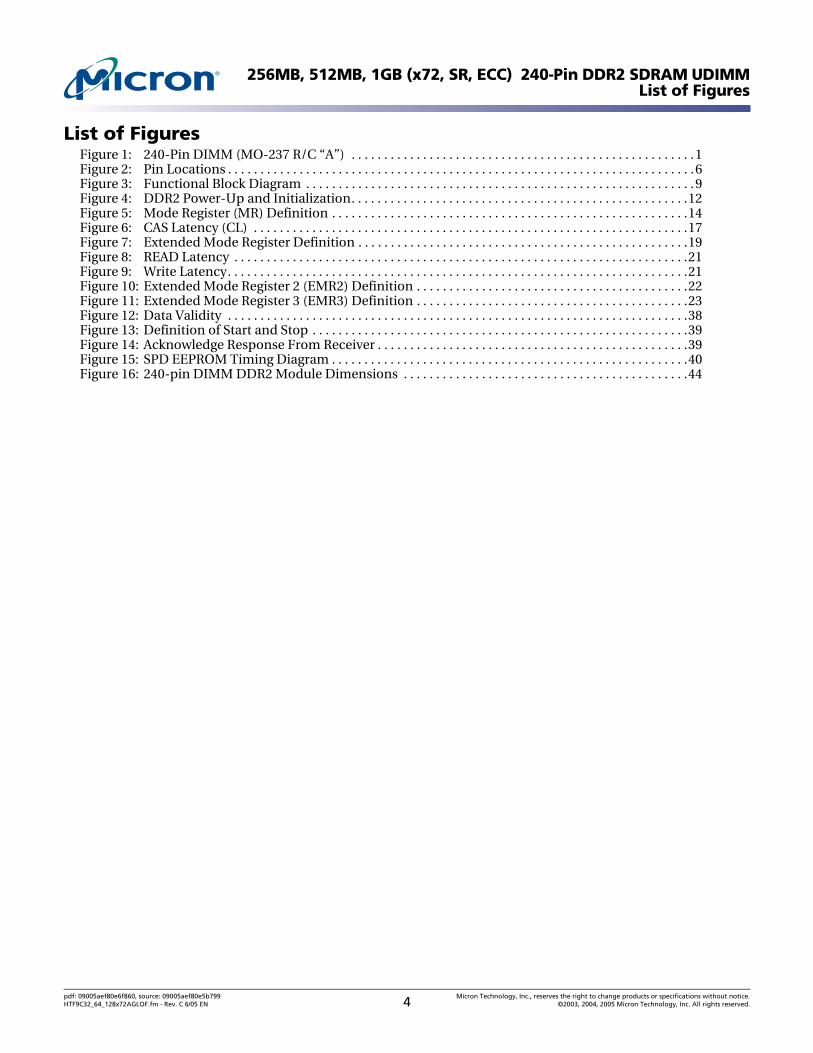
256MB, 512MB, 1GB (x72, SR, ECC) 240-Pin DDR2 SDRAM UDIMMList of Figures
List of FiguresFigure 1: 240-Pin DIMM (MO-237 R/C “A”) . . . . . . . . . . . . . . . . . . . . . . . . . . . . . . . . . . . . . . . . . . . . . . . . . . . . .1Figure 2: Pin Locations . . . . . . . . . . . . . . . . . . . . . . . . . . . . . . . . . . . . . . . . . . . . . . . . . . . . . . . . . . . . . . . . . . . . . . . .6Figure 3: Functional Block Diagram . . . . . . . . . . . . . . . . . . . . . . . . . . . . . . . . . . . . . . . . . . . . . . . . . . . . . . . . . . . .9Figure 4: DDR2 Power-Up and Initialization. . . . . . . . . . . . . . . . . . . . . . . . . . . . . . . . . . . . . . . . . . . . . . . . . . . .12Figure 5: Mode Register (MR) Definition . . . . . . . . . . . . . . . . . . . . . . . . . . . . . . . . . . . . . . . . . . . . . . . . . . . . . . .14Figure 6: CAS Latency (CL) . . . . . . . . . . . . . . . . . . . . . . . . . . . . . . . . . . . . . . . . . . . . . . . . . . . . . . . . . . . . . . . . . . .17Figure 7: Extended Mode Register Definition . . . . . . . . . . . . . . . . . . . . . . . . . . . . . . . . . . . . . . . . . . . . . . . . . . .19Figure 8: READ Latency . . . . . . . . . . . . . . . . . . . . . . . . . . . . . . . . . . . . . . . . . . . . . . . . . . . . . . . . . . . . . . . . . . . . . .21Figure 9: Write Latency. . . . . . . . . . . . . . . . . . . . . . . . . . . . . . . . . . . . . . . . . . . . . . . . . . . . . . . . . . . . . . . . . . . . . . .21Figure 10: Extended Mode Register 2 (EMR2) Definition . . . . . . . . . . . . . . . . . . . . . . . . . . . . . . . . . . . . . . . . . .22Figure 11: Extended Mode Register 3 (EMR3) Definition . . . . . . . . . . . . . . . . . . . . . . . . . . . . . . . . . . . . . . . . . .23Figure 12: Data Validity . . . . . . . . . . . . . . . . . . . . . . . . . . . . . . . . . . . . . . . . . . . . . . . . . . . . . . . . . . . . . . . . . . . . . . .38Figure 13: Definition of Start and Stop . . . . . . . . . . . . . . . . . . . . . . . . . . . . . . . . . . . . . . . . . . . . . . . . . . . . . . . . . .39Figure 14: Acknowledge Response From Receiver . . . . . . . . . . . . . . . . . . . . . . . . . . . . . . . . . . . . . . . . . . . . . . . .39Figure 15: SPD EEPROM Timing Diagram . . . . . . . . . . . . . . . . . . . . . . . . . . . . . . . . . . . . . . . . . . . . . . . . . . . . . . .40Figure 16: 240-pin DIMM DDR2 Module Dimensions . . . . . . . . . . . . . . . . . . . . . . . . . . . . . . . . . . . . . . . . . . . .44
pdf: 09005aef80e6f860, source: 09005aef80e5b799 Micron Technology, Inc., reserves the right to change products or specifications without notice.HTF9C32_64_128x72AGLOT.fm - Rev. C 6/05 EN 5 ©2003, 2004, 2005 Micron Technology, Inc. All rights reserved.
256MB, 512MB, 1GB (x72, SR, ECC) 240-Pin DDR2 SDRAM UDIMMList of Tables
List of TablesTable 1: Address Table . . . . . . . . . . . . . . . . . . . . . . . . . . . . . . . . . . . . . . . . . . . . . . . . . . . . . . . . . . . . . . . . . . . . . . .2Table 2: Key Timing Parameters . . . . . . . . . . . . . . . . . . . . . . . . . . . . . . . . . . . . . . . . . . . . . . . . . . . . . . . . . . . . . . .2Table 3: Part Numbers and Timing Parameters . . . . . . . . . . . . . . . . . . . . . . . . . . . . . . . . . . . . . . . . . . . . . . . . .2Table 4: Pin Assignment . . . . . . . . . . . . . . . . . . . . . . . . . . . . . . . . . . . . . . . . . . . . . . . . . . . . . . . . . . . . . . . . . . . . . .6Table 5: Pin Descriptions . . . . . . . . . . . . . . . . . . . . . . . . . . . . . . . . . . . . . . . . . . . . . . . . . . . . . . . . . . . . . . . . . . . . .7Table 6: Burst Definition. . . . . . . . . . . . . . . . . . . . . . . . . . . . . . . . . . . . . . . . . . . . . . . . . . . . . . . . . . . . . . . . . . . . .15Table 7: Commands Truth Table . . . . . . . . . . . . . . . . . . . . . . . . . . . . . . . . . . . . . . . . . . . . . . . . . . . . . . . . . . . . .24Table 8: Absolute Maximum DC Ratings . . . . . . . . . . . . . . . . . . . . . . . . . . . . . . . . . . . . . . . . . . . . . . . . . . . . . .25Table 9: Recommended DC Operating Conditions . . . . . . . . . . . . . . . . . . . . . . . . . . . . . . . . . . . . . . . . . . . . .25Table 10: Input DC Logic Levels . . . . . . . . . . . . . . . . . . . . . . . . . . . . . . . . . . . . . . . . . . . . . . . . . . . . . . . . . . . . . . .26Table 11: Input AC Logic Levels . . . . . . . . . . . . . . . . . . . . . . . . . . . . . . . . . . . . . . . . . . . . . . . . . . . . . . . . . . . . . . .26Table 12: General IDD Parameters . . . . . . . . . . . . . . . . . . . . . . . . . . . . . . . . . . . . . . . . . . . . . . . . . . . . . . . . . . . . .26Table 13: IDD7 Timing Patterns – 256MB and 512MB . . . . . . . . . . . . . . . . . . . . . . . . . . . . . . . . . . . . . . . . . . . .27Table 14: IDD7 Timing Patterns – 1GB . . . . . . . . . . . . . . . . . . . . . . . . . . . . . . . . . . . . . . . . . . . . . . . . . . . . . . . . . .27Table 15: DDR2 IDD Specifications and Conditions – 256MB. . . . . . . . . . . . . . . . . . . . . . . . . . . . . . . . . . . . . .28Table 16: DDR2 IDD Specifications and Conditions – 512MB. . . . . . . . . . . . . . . . . . . . . . . . . . . . . . . . . . . . . .29Table 17: DDR2 IDD Specifications and Conditions – 1GB . . . . . . . . . . . . . . . . . . . . . . . . . . . . . . . . . . . . . . . .30Table 18: AC Operating Conditions . . . . . . . . . . . . . . . . . . . . . . . . . . . . . . . . . . . . . . . . . . . . . . . . . . . . . . . . . . . .31Table 19: EEPROM Device Select Code . . . . . . . . . . . . . . . . . . . . . . . . . . . . . . . . . . . . . . . . . . . . . . . . . . . . . . . . .40Table 20: EEPROM Operating Modes . . . . . . . . . . . . . . . . . . . . . . . . . . . . . . . . . . . . . . . . . . . . . . . . . . . . . . . . . .40Table 21: Serial Presence-Detect EEPROM DC Operating Conditions. . . . . . . . . . . . . . . . . . . . . . . . . . . . . .41Table 22: Serial Presence-Detect EEPROM AC Operating Conditions . . . . . . . . . . . . . . . . . . . . . . . . . . . . . .41Table 23: Serial Presence-Detect Matrix . . . . . . . . . . . . . . . . . . . . . . . . . . . . . . . . . . . . . . . . . . . . . . . . . . . . . . . .42
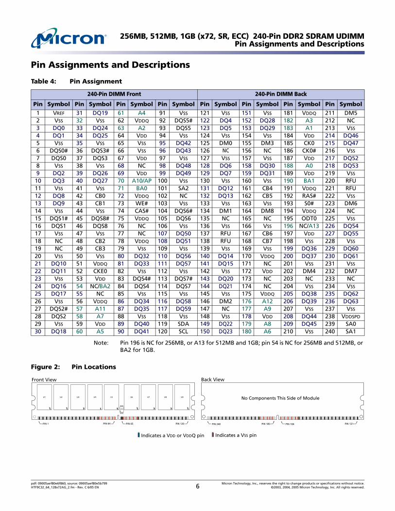
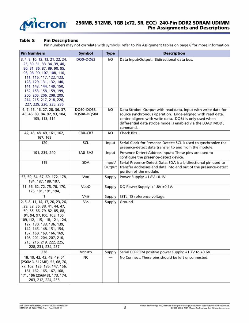
256MB, 512MB, 1GB (x72, SR, ECC) 240-Pin DDR2 SDRAM UDIMMPin Assignments and Descriptions
Pin Assignments and Descriptions
Note: Pin 196 is NC for 256MB, or A13 for 512MB and 1GB; pin 54 is NC for 256MB and 512MB, or BA2 for 1GB.
Figure 2: Pin Locations
Table 4: Pin Assignment
240-Pin DIMM Front 240-Pin DIMM Back
Pin Symbol Pin Symbol Pin Symbol Pin Symbol Pin Symbol Pin Symbol Pin Symbol Pin Symbol
1 VREF 31 DQ19 61 A4 91 VSS 121 VSS 151 VSS 181 VDDQ 211 DM52 VSS 32 VSS 62 VDDQ 92 DQS5# 122 DQ4 152 DQ28 182 A3 212 NC3 DQ0 33 DQ24 63 A2 93 DQS5 123 DQ5 153 DQ29 183 A1 213 VSS
4 DQ1 34 DQ25 64 VDD 94 VSS 124 VSS 154 VSS 184 VDD 214 DQ465 VSS 35 VSS 65 VSS 95 DQ42 125 DM0 155 DM3 185 CK0 215 DQ476 DQS0# 36 DQS3# 66 VSS 96 DQ43 126 NC 156 NC 186 CK0# 216 VSS
7 DQS0 37 DQS3 67 VDD 97 VSS 127 VSS 157 VSS 187 VDD 217 DQ528 VSS 38 VSS 68 NC 98 DQ48 128 DQ6 158 DQ30 188 A0 218 DQ539 DQ2 39 DQ26 69 VDD 99 DQ49 129 DQ7 159 DQ31 189 VDD 219 VSS
10 DQ3 40 DQ27 70 A10/AP 100 VSS 130 VSS 160 VSS 190 BA1 220 RFU11 VSS 41 VSS 71 BA0 101 SA2 131 DQ12 161 CB4 191 VDDQ 221 RFU12 DQ8 42 CB0 72 VDDQ 102 NC 132 DQ13 162 CB5 192 RAS# 222 VSS
13 DQ9 43 CB1 73 WE# 103 VSS 133 VSS 163 VSS 193 S0# 223 DM614 VSS 44 VSS 74 CAS# 104 DQS6# 134 DM1 164 DM8 194 VDDQ 224 NC15 DQS1# 45 DQS8# 75 VDDQ 105 DQS6 135 NC 165 NC 195 ODT0 225 VSS
16 DQS1 46 DQS8 76 NC 106 VSS 136 VSS 166 VSS 196 NC/A13 226 DQ5417 VSS 47 VSS 77 NC 107 DQ50 137 RFU 167 CB6 197 VDD 227 DQ5518 NC 48 CB2 78 VDDQ 108 DQ51 138 RFU 168 CB7 198 VSS 228 VSS
19 NC 49 CB3 79 VSS 109 VSS 139 VSS 169 VSS 199 DQ36 229 DQ6020 VSS 50 VSS 80 DQ32 110 DQ56 140 DQ14 170 VDDQ 200 DQ37 230 DQ6121 DQ10 51 VDDQ 81 DQ33 111 DQ57 141 DQ15 171 NC 201 VSS 231 VSS
22 DQ11 52 CKE0 82 VSS 112 VSS 142 VSS 172 VDD 202 DM4 232 DM723 VSS 53 VDD 83 DQS4# 113 DQS7# 143 DQ20 173 NC 203 NC 233 NC24 DQ16 54 NC/BA2 84 DQS4 114 DQS7 144 DQ21 174 NC 204 VSS 234 VSS
25 DQ17 55 NC 85 VSS 115 VSS 145 VSS 175 VDDQ 205 DQ38 235 DQ6226 VSS 56 VDDQ 86 DQ34 116 DQ58 146 DM2 176 A12 206 DQ39 236 DQ6327 DQS2# 57 A11 87 DQ35 117 DQ59 147 NC 177 A9 207 VSS 237 VSS
28 DQS2 58 A7 88 VSS 118 VSS 148 VSS 178 VDD 208 DQ44 238 VDDSPD
29 VSS 59 VDD 89 DQ40 119 SDA 149 DQ22 179 A8 209 DQ45 239 SA030 DQ18 60 A5 90 DQ41 120 SCL 150 DQ23 180 A6 210 VSS 240 SA1
U1 U2 U3 U4
U10
U6 U7 U8 U9 No Components This Side of Module
PIN 121PIN 184PIN 185PIN 240PIN 1 PIN 64 PIN 65 PIN 120
Front View Back View
Indicates a VDD or VDDQ pin Indicates a VSS pin
U5
pdf: 09005aef80e6f860, source: 09005aef80e5b799 Micron Technology, Inc., reserves the right to change products or specifications without notice.HTF9C32_64_128x72AG_2.fm - Rev. C 6/05 EN 6 ©2003, 2004, 2005 Micron Technology, Inc. All rights reserved.
256MB, 512MB, 1GB (x72, SR, ECC) 240-Pin DDR2 SDRAM UDIMMPin Assignments and Descriptions
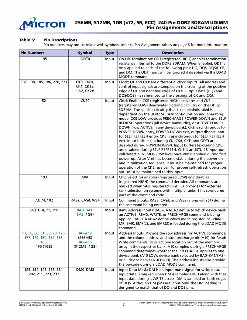
Table 5: Pin DescriptionsPin numbers may not correlate with symbols; refer to Pin Assignment tables on page 6 for more information
Pin Numbers Symbol Type Description
195 ODT0 Input On-Die Termination: ODT (registered HIGH) enables termination resistance internal to the DDR2 SDRAM. When enabled, ODT is only applied to each of the following pins: DQ, DQS, DQS#, CB, and DM. The ODT input will be ignored if disabled via the LOAD MODE command.
137, 138, 185, 186, 220, 221 CK0, CK0#,CK1, CK1#,CK2, CK2#
Input Clock: CK and CK# are differential clock inputs. All address and control input signals are sampled on the crossing of the positive edge of CK and negative edge of CK#. Output data (DQs and DQS/DQS#) is referenced to the crossings of CK and CK#.
52 CKE0 Input Clock Enable: CKE (registered HIGH) activates and CKE (registered LOW) deactivates clocking circuitry on the DDR2 SDRAM. The specific circuitry that is enabled/disabled is dependent on the DDR2 SDRAM configuration and operating mode. CKE LOW provides PRECHARGE POWER-DOWN and SELF REFRESH operations (all device banks idle), or ACTIVE POWER-DOWN (row ACTIVE in any device bank). CKE is synchronous for POWER-DOWN entry, POWER-DOWN exit, output disable, and for SELF REFRESH entry. CKE is asynchronous for SELF REFRESH exit. Input buffers (excluding CK, CK#, CKE, and ODT) are disabled during POWER-DOWN. Input buffers (excluding CKE) are disabled during SELF REFRESH. CKE is an SSTL_18 input but will detect a LVCMOS LOW level once VDD is applied during first power-up. After Vref has become stable during the power on and initialization sequence, it must be maintained for proper operation of the CKE receiver. For proper self-refresh operation VREF must be maintained to this input.
193 S0# Input Chip Select: S# enables (registered LOW) and disables (registered HIGH) the command decoder. All commands are masked when S# is registered HIGH. S# provides for external rank selection on systems with multiple ranks. S# is considered part of the command code.
73, 74, 192 RAS#, CAS#, WE# Input Command Inputs: RAS#, CAS#, and WE# (along with S#) define the command being entered.
54 (1GB), 71, 190 BA0, BA1, BA2 (1GB)
Input Bank Address Inputs: BA0–BA1/BA2 define to which device bank an ACTIVE, READ, WRITE, or PRECHARGE command is being applied. BA0–BA1/BA2 define which mode register including MR, EMR, EMR(2), and EMR(3) is loaded during the LOAD MODE command.
57, 58, 60, 61, 63, 70, 176, 177, 179, 180, 182, 183,
188,196 (1GB)
A0–A12 (256MB)A0–A13
(512MB, 1GB)
Input Address Inputs: Provide the row address for ACTIVE commands, and the column address and auto precharge bit (A10) for Read/Write commands, to select one location out of the memory array in the respective bank. A10 sampled during a PRECHARGE command determines whether the PRECHARGE applies to one device bank (A10 LOW, device bank selected by BA0–BA1/BA2) or all device banks (A10 HIGH). The address inputs also provide the op-code during a LOAD MODE command.
125, 134, 146, 155, 164, 202, 211, 223, 232
DM0–DM8 Input Input Data Mask: DM is an input mask signal for write data. Input data is masked when DM is sampled HIGH along with that input data during a WRITE access. DM is sampled on both edges of DQS. Although DM pins are input-only, the DM loading is designed to match that of DQ and DQS pins.
pdf: 09005aef80e6f860, source: 09005aef80e5b799 Micron Technology, Inc., reserves the right to change products or specifications without notice.HTF9C32_64_128x72AG_2.fm - Rev. C 6/05 EN 7 ©2003, 2004, 2005 Micron Technology, Inc. All rights reserved.
256MB, 512MB, 1GB (x72, SR, ECC) 240-Pin DDR2 SDRAM UDIMMPin Assignments and Descriptions
3, 4, 9, 10, 12, 13, 21, 22, 24, 25, 30, 31, 33, 34, 39, 40, 80, 81, 86, 87, 89, 90, 95, 96, 98, 99, 107, 108, 110, 111, 116, 117, 122, 123, 128, 129, 131, 132, 140, 141, 143, 144, 149, 150, 152, 153, 158, 159, 199, 200, 205, 206, 208, 209, 214, 215, 217, 218, 226, 227, 229, 230, 235, 236
DQ0–DQ63 I/O Data Input/Output: Bidirectional data bus.
6, 7, 15, 16, 27, 28, 36, 37, 45, 46, 83, 84, 92, 93, 104,
105, 113, 114
DQS0–DQS8,DQS0#–DQS8#
I/O Data Strobe: Output with read data, input with write data for source synchronous operation. Edge-aligned with read data, center aligned with write data. DQS# is only used when differential data strobe mode is enabled via the LOAD MODE command.
42, 43, 48, 49, 161, 162, 167, 168
CB0–CB7 I/O Check Bits.
120 SCL Input Serial Clock for Presence-Detect: SCL is used to synchronize the presence-detect data transfer to and from the module.
101, 239, 240 SA0–SA2 Input Presence-Detect Address Inputs: These pins are used to configure the presence-detect device.
119 SDA Input/Output
Serial Presence-Detect Data: SDA is a bidirectional pin used to transfer addresses and data into and out of the presence-detect portion of the module.
53, 59, 64, 67, 69, 172, 178, 184, 187, 189, 197,
VDD Supply Power Supply: +1.8V ±0.1V.
51, 56, 62, 72, 75, 78, 170, 175, 181, 191, 194,
VDDQ Supply DQ Power Supply: +1.8V ±0.1V.
1 VREF Supply SSTL_18 reference voltage.2, 5, 8, 11, 14, 17, 20, 23, 26,
29, 32, 35, 38, 41, 44, 47, 50, 65, 66, 79, 82, 85, 88, 91, 94, 97,100, 103, 106,
109,112, 115, 118, 121, 124, 127, 130, 133, 136, 139, 142, 145, 148, 151, 154, 157, 160, 163, 166, 169, 198, 201, 204, 207, 210, 213, 216, 219, 222, 225,
228, 231, 234, 237
VSS Supply Ground.
238 VDDSPD Supply Serial EEPROM positive power supply: +1.7V to +3.6V.18, 19, 42, 43, 48, 49, 54
(256MB, 512MB), 55, 68, 76, 77, 102, 126, 135, 147, 156,
161, 162, 165, 167, 168, 171, 196 (256MB), 173, 174,
203, 212, 224, 233
NC — No Connect: These pins should be left unconnected.
Table 5: Pin DescriptionsPin numbers may not correlate with symbols; refer to Pin Assignment tables on page 6 for more information
Pin Numbers Symbol Type Description
pdf: 09005aef80e6f860, source: 09005aef80e5b799 Micron Technology, Inc., reserves the right to change products or specifications without notice.HTF9C32_64_128x72AG_2.fm - Rev. C 6/05 EN 8 ©2003, 2004, 2005 Micron Technology, Inc. All rights reserved.
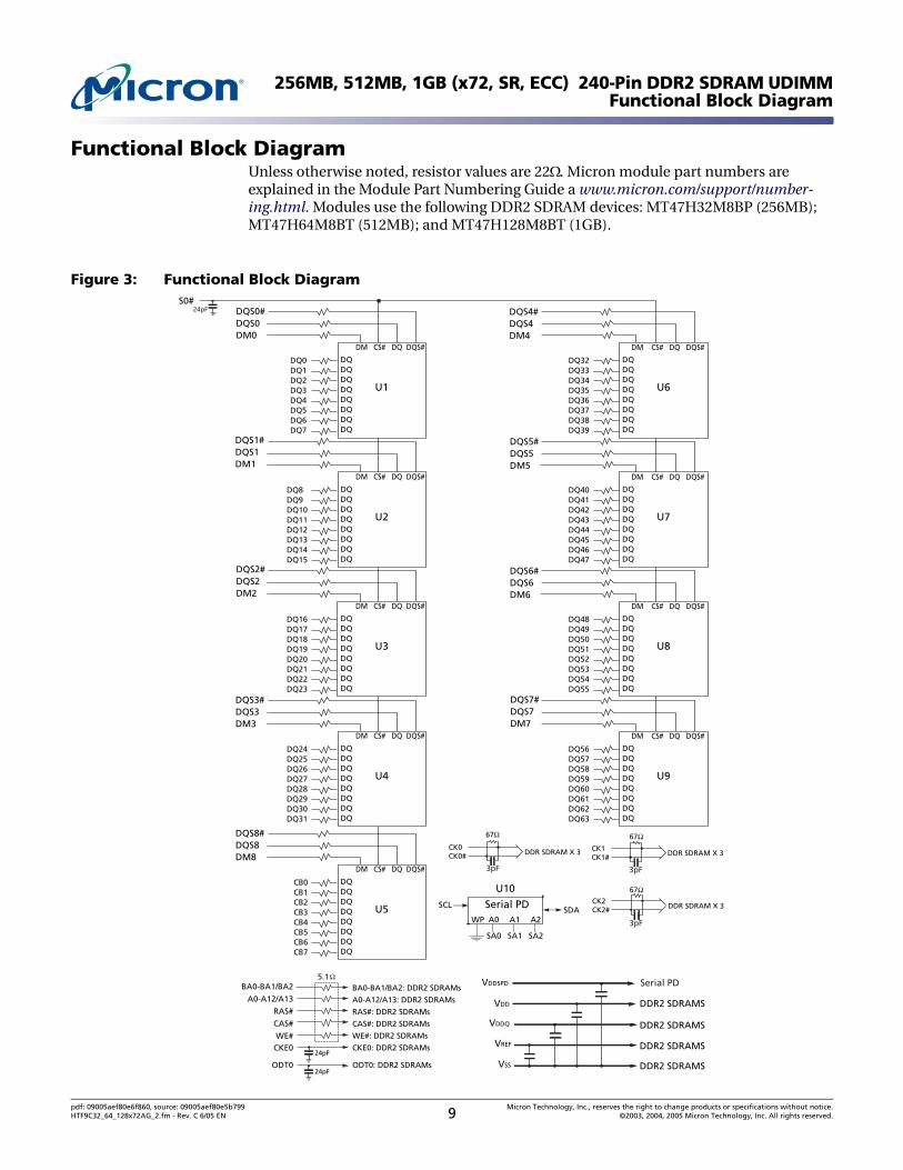
256MB, 512MB, 1GB (x72, SR, ECC) 240-Pin DDR2 SDRAM UDIMMFunctional Block Diagram
Functional Block DiagramUnless otherwise noted, resistor values are 22Ω. Micron module part numbers are explained in the Module Part Numbering Guide a www.micron.com/support/number-ing.html. Modules use the following DDR2 SDRAM devices: MT47H32M8BP (256MB); MT47H64M8BT (512MB); and MT47H128M8BT (1GB).
Figure 3: Functional Block Diagram
DQDQDQDQDQDQDQDQ
DQ0DQ1DQ2DQ3DQ4DQ5DQ6DQ7
U1
DM CS# DQ DQS#
DQDQDQDQDQDQDQDQ
DQ32DQ33DQ34DQ35DQ36DQ37DQ38DQ39
U6
DM CS# DQ DQS#
DQDQDQDQDQDQDQDQ
DQ8DQ9DQ10DQ11DQ12DQ13DQ14DQ15
U2
DM CS# DQ DQS#
DQDQDQDQDQDQDQDQ
DQ16DQ17DQ18DQ19DQ20DQ21DQ22DQ23
U3
DM CS# DQ DQS#
DQDQDQDQDQDQDQDQ
DQ24DQ25DQ26DQ27DQ28DQ29DQ30DQ31
U4
DM CS# DQ DQS#
DQDQDQDQDQDQDQDQ
DQ40DQ41DQ42DQ43DQ44DQ45DQ46DQ47
U7
DM CS# DQ DQS#
DQDQDQDQDQDQDQDQ
DQ48DQ49DQ50DQ51DQ52DQ53DQ54DQ55
U8
DM CS# DQ DQS#
DQDQDQDQDQDQDQDQ
DQ56DQ57DQ58DQ59DQ60DQ61DQ62DQ63
U9
DM CS# DQ DQS#
DQS0#DQS0DM0
S0#
DQS1#DQS1DM1
DQS2#DQS2DM2
DQS3#DQS3DM3
DQS4#DQS4DM4
DQS5#DQS5DM5
DQS6#DQS6DM6
DQS7#DQS7DM7
DDR SDRAM X 3CK0CK0# DDR SDRAM X 3
CK1CK1#
DDR SDRAM X 3CK2CK2#
A0
Serial PDA1 A2
SA0 SA1 SA2
SDASCL
WP
U10
BA0-BA1/BA2
A0-A12/A13
RAS#
CAS#
WE#CKE0
ODT0
BA0-BA1/BA2: DDR2 SDRAMs
A0-A12/A13: DDR2 SDRAMs
RAS#: DDR2 SDRAMs
CAS#: DDR2 SDRAMs
WE#: DDR2 SDRAMs
CKE0: DDR2 SDRAMs
ODT0: DDR2 SDRAMs
VREF
VSS
DDR2 SDRAMS
DDR2 SDRAMS
VDD
DDR2 SDRAMS
VDDSPD Serial PD
VDDQ
DDR2 SDRAMS
3pF 3pF
3pF
5.1
24pF
24pF
24pF
DQDQDQDQDQDQDQDQ
CB0CB1CB2CB3CB4CB5CB6CB7
U5
DM CS# DQ DQS#
DQS8#DQS8DM8
67Ω 67Ω
67Ω
pdf: 09005aef80e6f860, source: 09005aef80e5b799 Micron Technology, Inc., reserves the right to change products or specifications without notice.HTF9C32_64_128x72AG_2.fm - Rev. C 6/05 EN 9 ©2003, 2004, 2005 Micron Technology, Inc. All rights reserved.
256MB, 512MB, 1GB (x72, SR, ECC) 240-Pin DDR2 SDRAM UDIMMGeneral Description
General DescriptionThe MT9HTF3272A, MT9HTF6472A, and MT9HTF12872A DDR2 SDRAM modules are high-speed, CMOS, dynamic random-access 256MB, 512MB, and 1GB memory modules organized in x64 configuration. DDR2 SDRAM modules use internally configured quad-bank (256MB, 512MB) or eight-bank (1GB) DDR2 SDRAM devices.
DDR2 SDRAM modules use double data rate architecture to achieve high-speed opera-tion. The double data rate architecture is essentially a 4n-prefetch architecture with an interface designed to transfer two data words per clock cycle at the I/O pins. A single read or write access for the DDR2 SDRAM module effectively consists of a single 4n-bit-wide, one-clock-cycle data transfer at the internal DRAM core and four corresponding n-bit-wide, one-half-clock-cycle data transfers at the I/O pins.
A bidirectional data strobe (DQS, DQS#) is transmitted externally, along with data, for use in data capture at the receiver. DQS is a strobe transmitted by the DDR2 SDRAM device during READs and by the memory controller during WRITEs. DQS is edge-aligned with data for READs and center-aligned with data for WRITEs.
DDR2 SDRAM modules operate from a differential clock (CK and CK#); the crossing of CK going HIGH and CK# going LOW will be referred to as the positive edge of CK. Com-mands (address and control signals) are registered at every positive edge of CK. Input data is registered on both edges of DQS, and output data is referenced to both edges of DQS, as well as to both edges of CK.
Read and write accesses to DDR2 SDRAM modules are burst-oriented; accesses start at a selected location and continue for a programmed number of locations in a programmed sequence. Accesses begin with the registration of an ACTIVE command, which is then followed by a READ or WRITE command. The address bits registered coincident with the ACTIVE command are used to select the device bank and row to be accessed. The address bits registered coincident with the READ or WRITE command are used to select the device bank and the starting column location for the burst access.
DDR2 SDRAM modules provide for programmable read or write burst lengths of four or eight locations. DDR2 SDRAM devices support interrupting a burst read of eight with another read, or a burst write of eight with another write. An auto precharge function may be enabled to provide a self-timed row precharge that is initiated at the end of the burst access.
The pipelined, multibank architecture of DDR2 SDRAM devices allows for concurrent operation, thereby providing high, effective bandwidth by hiding row precharge and activation time.
A self refresh mode is provided, along with a power-saving power-down mode.
All inputs are compatible with the JEDEC standard for SSTL_18. All full drive-strength outputs are SSTL_18-compatible.
Serial Presence-Detect OperationDDR2 SDRAM modules incorporate serial presence-detect (SPD). The SPD function is implemented using a 2,048-bit EEPROM. This nonvolatile storage device contains 256 bytes. The first 128 bytes can be programmed by Micron to identify the module type and various SDRAM organizations and timing parameters. The remaining 128 bytes of stor-age are available for use by the customer. System READ/WRITE operations between the master (system logic) and the slave EEPROM device occur via a standard I2C bus using the DIMM’s SCL (clock) and SDA (data) signals, together with SA (2:0), which provide eight unique DIMM/EEPROM addresses. Write protect (WP) is tied to ground on the module, permanently disabling hardware write protect.
pdf: 09005aef80e6f860, source: 09005aef80e5b799 Micron Technology, Inc., reserves the right to change products or specifications without notice.HTF9C32_64_128x72AG_2.fm - Rev. C 6/05 EN 10 ©2003, 2004, 2005 Micron Technology, Inc. All rights reserved.
256MB, 512MB, 1GB (x72, SR, ECC) 240-Pin DDR2 SDRAM UDIMMInitialization
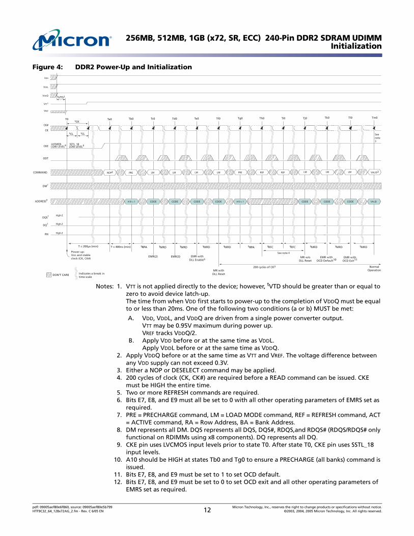
InitializationThe following sequence is required for power-up and initialization and is shown in Figure 4, DDR2 Power-Up and Initialization, on page 12.
1. Apply power; if CKE is maintained below 20 percent of VDDQ, outputs remain dis-abled. To guarantee RTT (ODT Resistance) is off, VREF must be valid and a low levelmust be applied to the ODT pin (all other inputs may be undefined). The time fromwhen VDD first starts to power-up to the completion of VDDQ must be equal to or lessthan 20ms. At least one of the following two sets of conditions (A or B) must be met:
A. CONDITION SET A• VDD, VDDL and VDDQ are driven from a single power converter output• VTT is limited to 0.95V MAX• VREF tracks VDDQ/2
B. CONDITION SET B• Apply VDD before or at the same time as VDDL.• Apply VDDL before or at the same time as VDDQ• Apply VDDQ before or at the same time as VTT and VREF
3. The voltage difference between any VDD supply can not exceed 0.3V. For a minimumof 200µs after stable power and clock (CK, CK#), apply NOP or DESELECT commandsand take CKE HIGH
4. Wait a minimum of 400ns, then issue a PRECHARGE ALL command.5. Issue a LOAD MODE command to the EMR(2) register. (To issue an EMR(2) com-
mand, provide LOW to BA0 and BA2, provide HIGH to BA1.)6. Issue a LOAD MODE command to the EMR(3) register. (To issue an EMR(3) com-
mand, provide HIGH to BA0 and BA1, provide LOW to BA2.)7. Issue a LOAD MODE command to the EMR register to enable DLL. To issue a DLL
ENABLE command, provide LOW to BA1, BA2, and A0, provide HIGH to BA0. Bits E7,E8, and E9 must all be set to 0.
8. Issue a LOAD MODE command for DLL Reset. 200 cycles of clock input is required tolock the DLL. (To issue a DLL Reset, provide HIGH to A8 and provide LOW to BA2, BA1and BA0.) CKE must be HIGH the entire time.
9. Issue PRECHARGE ALL command.10. Issue two or more REFRESH commands.11. Issue a LOAD MODE command with LOW to A8 to initialize device operation (i.e., to
program operating parameters without resetting the DLL).12. Issue a LOAD MODE command to the EMR to enable OCD default by setting Bits E7,
E8, and E9 to 1 and set all other desired parameters.13. Issue a LOAD MODE command to the EMR to enable OCD exit by setting Bits E7, E8,
and E9 to 0 and set all other desired parameters.The DDR2 SDRAM device is now intialized and ready for normal operation 200 clocks after DLL Reset in step 8.
pdf: 09005aef80e6f860, source: 09005aef80e5b799 Micron Technology, Inc., reserves the right to change products or specifications without notice.HTF9C32_64_128x72AG_2.fm - Rev. C 6/05 EN 11 ©2003, 2004, 2005 Micron Technology, Inc. All rights reserved.
256MB, 512MB, 1GB (x72, SR, ECC) 240-Pin DDR2 SDRAM UDIMMInitialization
Figure 4: DDR2 Power-Up and Initialization
Notes: 1. VTT is not applied directly to the device; however, tVTD should be greater than or equal to zero to avoid device latch-up.The time from when VDD first starts to power-up to the completion of VDDQ must be equal to or less than 20ms. One of the following two conditions (a or b) MUST be met:
A. VDD, VDDL, and VDDQ are driven from a single power converter output.VTT may be 0.95V maximum during power up.VREF tracks VDDQ/2.
B. Apply VDD before or at the same time as VDDL.Apply VDDL before or at the same time as VDDQ.
2. Apply VDDQ before or at the same time as VTT and VREF. The voltage difference between any VDD supply can not exceed 0.3V.
3. Either a NOP or DESELECT command may be applied.4. 200 cycles of clock (CK, CK#) are required before a READ command can be issued. CKE
must be HIGH the entire time.5. Two or more REFRESH commands are required.6. Bits E7, E8, and E9 must all be set to 0 with all other operating parameters of EMRS set as
required.7. PRE = PRECHARGE command, LM = LOAD MODE command, REF = REFRESH command, ACT
= ACTIVE command, RA = Row Address, BA = Bank Address.8. DM represents all DM. DQS represents all DQS, DQS#, RDQS,and RDQS# (RDQS/RDQS# only
functional on RDIMMs using x8 components). DQ represents all DQ.9. CKE pin uses LVCMOS input levels prior to state T0. After state T0, CKE pin uses SSTL_18
input levels. 10. A10 should be HIGH at states Tb0 and Tg0 to ensure a PRECHARGE (all banks) command is
issued.11. Bits E7, E8, and E9 must be set to 1 to set OCD default.12. Bits E7, E8, and E9 must be set to 0 to set OCD exit and all other operating parameters of
EMRS set as required.
tVTD1
CKE
Rtt
Power-up:VDD and stableclock (CK, CK#)
T = 200µs (min)
High-Z
DM7
DQS7 High-Z
ADDRESS9
CK
CK#
tCL
VTT1
VREF
VDDL
VDDQ
COMMAND NOP2 PRE
T0 Ta0
DON’T CARE
tCL
tCK
VDD
ODT
DQ7 High-Z
T = 400ns (min)
Tb0
200 cycles of CK3
EMR withDLL Enable5
MR withDLL Reset
tMRD tMRD t tRFC tRFC
LM PRELM REF REF LM
Tg0 Th0 Ti0 Tj0
MR w/oDLL Reset
EMR withOCD Default10
tMRD tMRD tMRD
Tk0 Tl0 Tm0Te0 Tf0
EMR(2) EMR(3)
tMRD tMRD
LMLM
A10 = 1
tRPA
Tc0 Td0
LVCMOS LOW LEVEL8 SSTL_18
LOW LEVEL8
VALID3
VALID
Indicates a break in time scale
RPA
LM
EMR withOCD Exit11
LM
NormalOperation
See note 4
See note 3
CODE CODE A10 = 1CODE CODE CODE CODE CODE
pdf: 09005aef80e6f860, source: 09005aef80e5b799 Micron Technology, Inc., reserves the right to change products or specifications without notice.HTF9C32_64_128x72AG_2.fm - Rev. C 6/05 EN 12 ©2003, 2004, 2005 Micron Technology, Inc. All rights reserved.
256MB, 512MB, 1GB (x72, SR, ECC) 240-Pin DDR2 SDRAM UDIMMMode Register (MR)
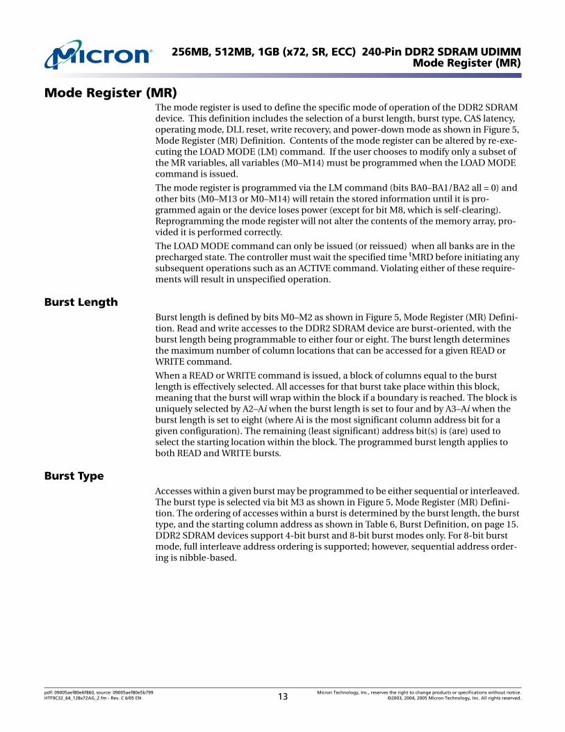
Mode Register (MR)The mode register is used to define the specific mode of operation of the DDR2 SDRAM device. This definition includes the selection of a burst length, burst type, CAS latency, operating mode, DLL reset, write recovery, and power-down mode as shown in Figure 5, Mode Register (MR) Definition. Contents of the mode register can be altered by re-exe-cuting the LOAD MODE (LM) command. If the user chooses to modify only a subset of the MR variables, all variables (M0–M14) must be programmed when the LOAD MODE command is issued.
The mode register is programmed via the LM command (bits BA0–BA1/BA2 all = 0) and other bits (M0–M13 or M0–M14) will retain the stored information until it is pro-grammed again or the device loses power (except for bit M8, which is self-clearing). Reprogramming the mode register will not alter the contents of the memory array, pro-vided it is performed correctly.
The LOAD MODE command can only be issued (or reissued) when all banks are in the precharged state. The controller must wait the specified time tMRD before initiating any subsequent operations such as an ACTIVE command. Violating either of these require-ments will result in unspecified operation.
Burst LengthBurst length is defined by bits M0–M2 as shown in Figure 5, Mode Register (MR) Defini-tion. Read and write accesses to the DDR2 SDRAM device are burst-oriented, with the burst length being programmable to either four or eight. The burst length determines the maximum number of column locations that can be accessed for a given READ or WRITE command.
When a READ or WRITE command is issued, a block of columns equal to the burst length is effectively selected. All accesses for that burst take place within this block, meaning that the burst will wrap within the block if a boundary is reached. The block is uniquely selected by A2–Ai when the burst length is set to four and by A3–Ai when the burst length is set to eight (where Ai is the most significant column address bit for a given configuration). The remaining (least significant) address bit(s) is (are) used to select the starting location within the block. The programmed burst length applies to both READ and WRITE bursts.
Burst TypeAccesses within a given burst may be programmed to be either sequential or interleaved. The burst type is selected via bit M3 as shown in Figure 5, Mode Register (MR) Defini-tion. The ordering of accesses within a burst is determined by the burst length, the burst type, and the starting column address as shown in Table 6, Burst Definition, on page 15. DDR2 SDRAM devices support 4-bit burst and 8-bit burst modes only. For 8-bit burst mode, full interleave address ordering is supported; however, sequential address order-ing is nibble-based.
pdf: 09005aef80e6f860, source: 09005aef80e5b799 Micron Technology, Inc., reserves the right to change products or specifications without notice.HTF9C32_64_128x72AG_2.fm - Rev. C 6/05 EN 13 ©2003, 2004, 2005 Micron Technology, Inc. All rights reserved.
256MB, 512MB, 1GB (x72, SR, ECC) 240-Pin DDR2 SDRAM UDIMMMode Register (MR)
Figure 5: Mode Register (MR) Definition
Burst LengthCAS# Latency BTPD
A9 A7 A6 A5 A4 A3A8 A2 A1 A0
Mode Register (Mx)
Address Bus
9 7 6 5 4 38 2 1 0
A10A12 A11BA0BA1
1011121314DLL TMWRMR
Burst LengthCAS# Latency BTPD
A9 A7 A6 A5 A4 A3A8 A2 A1 A0
Mode Register (Mx)
Address Bus
9 7 6 5 4 38 2 1 0
A10A12 A11BA0BA1
101112130*
1415DLL TMWR
A13
MR
256MB Address Bus
512MB Address Bus
Burst LengthCAS# Latency BTPD
A9 A7 A6 A5 A4 A3A8 A2 A1 A0
Mode Register (Mx)
Address Bus
9 7 6 5 4 38 2 1 0
A10A12 A11BA0BA1
101112130*
14
Burst Length
Reserved
Reserved
4
8
Reserved
Reserved
Reserved
Reserved
M0
0
1
0
1
0
1
0
1
M1
0
0
1
1
0
0
1
1
M2
0
0
0
0
1
1
1
1
0
1
Burst Type
Sequential
Interleaved
M3
CAS Latency
Reserved
Reserved
Reserved
3
4
Reserved
Reserved
Reserved
M4
0
1
0
1
0
1
0
1
M5
0
0
1
1
0
0
1
1
M6
0
0
0
0
1
1
1
1
0
1
Mode
Normal
Test
M7
15DLL TM
0
1
DLL Reset
No
Yes
M8
WRITE RECOVERY
Reserved
2
3
4
5
6
Reserved
Reserved
M9
0
1
0
1
0
1
0
1
M10
0
0
1
1
0
0
1
1
M11
0
0
0
0
1
1
1
1
WR
A13
MR
0
1
0
1
Mode Register Definition
Mode Register (MR)
Extended Mode Register (EMR)
Extended Mode Register (EMR2)
Extended Mode Register (EMR3)
M15
0
0
1
1
0
1
PD mode
Fast Exit
(Normal)
Slow Exit
(Low Power)
M12
M14
BA2
160*
1GB Address Bus
pdf: 09005aef80e6f860, source: 09005aef80e5b799 Micron Technology, Inc., reserves the right to change products or specifications without notice.HTF9C32_64_128x72AG_2.fm - Rev. C 6/05 EN 14 ©2003, 2004, 2005 Micron Technology, Inc. All rights reserved.
256MB, 512MB, 1GB (x72, SR, ECC) 240-Pin DDR2 SDRAM UDIMMMode Register (MR)
Operating ModeThe normal operating mode is selected by issuing a LOAD MODE command with bit M7 set to zero, and all other bits set to the desired values as shown in Figure 5, Mode Register (MR) Definition, on page 14. When bit M7 is ‘1,’ no other bits of the mode register are programmed. Programming bit M7 to ‘1’ places the DDR2 SDRAM device into a test mode that is only used by the Manufacturer and should NOT be used. No operation or functionality is guaranteed if M7 bit is ‘1.’
DLL ResetDLL reset is defined by bit M8 as shown in Figure 5, Mode Register (MR) Definition, on page 14. Programming bit M8 to ‘1’ will activate the DLL RESET function. Bit M8 is self-clearing, meaning it returns back to a value of ‘0’ after the DLL RESET function has been issued.
Anytime the DLL RESET function is used, 200 clock cycles must occur before a READ command can be issued to allow time for the internal clock to be synchronized with the external clock. Failing to wait for synchronization to occur may result in a violation of the tAC or tDQSCK parameters.
Write RecoveryWrite recovery (WR) time is defined by bits M9–M11 as shown in Figure 5, Mode Register (MR) Definition, on page 14. The WR Register is used by the DDR2 SDRAM device during WRITE with AUTO PRECHARGE operation. During WRITE with AUTO PRECHARGE operation, the DDR2 SDRAM device delays the internal AUTO PRECHARGE operation by WR clocks (programmed in bits M9–M11) from the last data burst.
Write Recovery (WR) values of 2, 3, 4, 5, or 6 clocks may be used for programming bits M9–M11. The user is required to program the value of write recovery, which is calculated by dividing tWR (in ns) by tCK (in ns) and rounding up a noninteger value to the next integer; WR [cycles] = tWR [ns] / tCK [ns]. Reserved states should not be used as unknown operation or incompatibility with future versions may result.
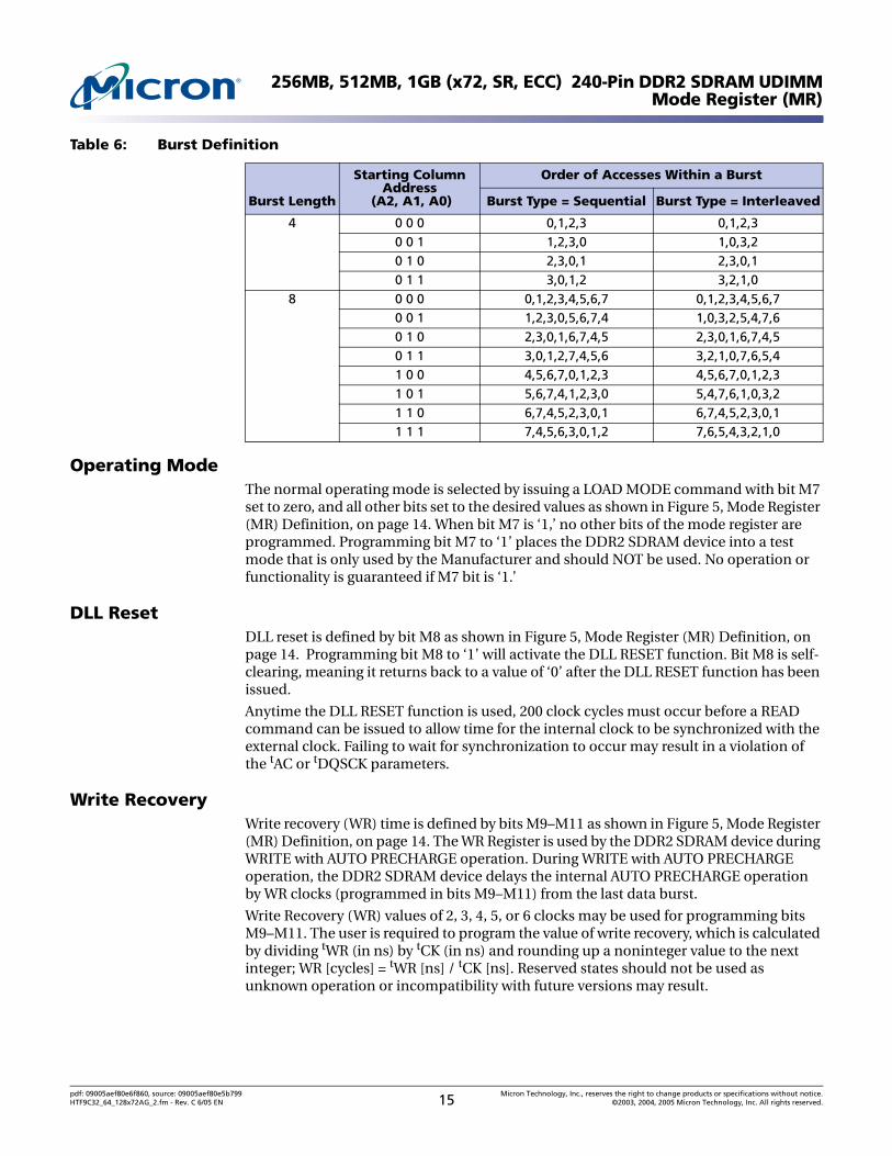
Table 6: Burst Definition
Burst Length
Starting Column Address
(A2, A1, A0)
Order of Accesses Within a Burst
Burst Type = Sequential Burst Type = Interleaved
4 0 0 0 0,1,2,3 0,1,2,30 0 1 1,2,3,0 1,0,3,20 1 0 2,3,0,1 2,3,0,10 1 1 3,0,1,2 3,2,1,0
8 0 0 0 0,1,2,3,4,5,6,7 0,1,2,3,4,5,6,70 0 1 1,2,3,0,5,6,7,4 1,0,3,2,5,4,7,60 1 0 2,3,0,1,6,7,4,5 2,3,0,1,6,7,4,50 1 1 3,0,1,2,7,4,5,6 3,2,1,0,7,6,5,41 0 0 4,5,6,7,0,1,2,3 4,5,6,7,0,1,2,31 0 1 5,6,7,4,1,2,3,0 5,4,7,6,1,0,3,21 1 0 6,7,4,5,2,3,0,1 6,7,4,5,2,3,0,11 1 1 7,4,5,6,3,0,1,2 7,6,5,4,3,2,1,0
pdf: 09005aef80e6f860, source: 09005aef80e5b799 Micron Technology, Inc., reserves the right to change products or specifications without notice.HTF9C32_64_128x72AG_2.fm - Rev. C 6/05 EN 15 ©2003, 2004, 2005 Micron Technology, Inc. All rights reserved.
256MB, 512MB, 1GB (x72, SR, ECC) 240-Pin DDR2 SDRAM UDIMMMode Register (MR)
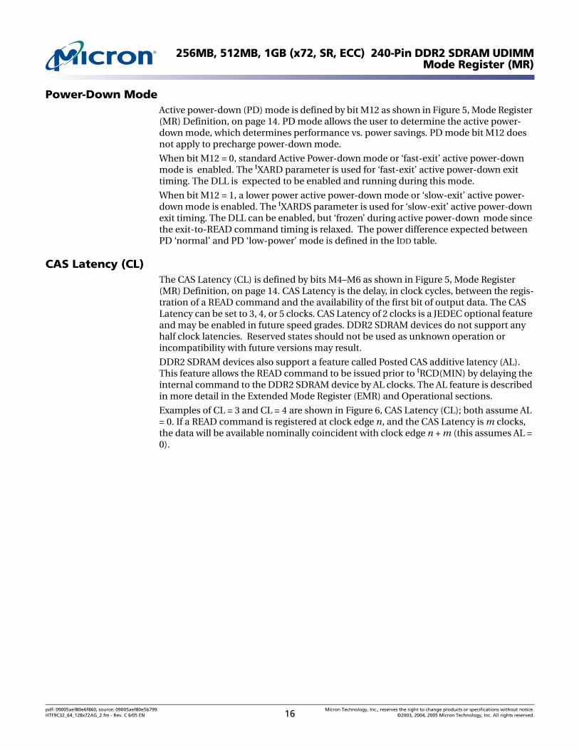
Power-Down ModeActive power-down (PD) mode is defined by bit M12 as shown in Figure 5, Mode Register (MR) Definition, on page 14. PD mode allows the user to determine the active power-down mode, which determines performance vs. power savings. PD mode bit M12 does not apply to precharge power-down mode.
When bit M12 = 0, standard Active Power-down mode or ‘fast-exit’ active power-down mode is enabled. The tXARD parameter is used for ‘fast-exit’ active power-down exit timing. The DLL is expected to be enabled and running during this mode.
When bit M12 = 1, a lower power active power-down mode or ‘slow-exit’ active power-down mode is enabled. The tXARDS parameter is used for ‘slow-exit’ active power-down exit timing. The DLL can be enabled, but ‘frozen’ during active power-down mode since the exit-to-READ command timing is relaxed. The power difference expected between PD ‘normal’ and PD ‘low-power’ mode is defined in the IDD table.
CAS Latency (CL)The CAS Latency (CL) is defined by bits M4–M6 as shown in Figure 5, Mode Register (MR) Definition, on page 14. CAS Latency is the delay, in clock cycles, between the regis-tration of a READ command and the availability of the first bit of output data. The CAS Latency can be set to 3, 4, or 5 clocks. CAS Latency of 2 clocks is a JEDEC optional feature and may be enabled in future speed grades. DDR2 SDRAM devices do not support any half clock latencies. Reserved states should not be used as unknown operation or incompatibility with future versions may result.
DDR2 SDRAM devices also support a feature called Posted CAS additive latency (AL). This feature allows the READ command to be issued prior to tRCD(MIN) by delaying the internal command to the DDR2 SDRAM device by AL clocks. The AL feature is described in more detail in the Extended Mode Register (EMR) and Operational sections.
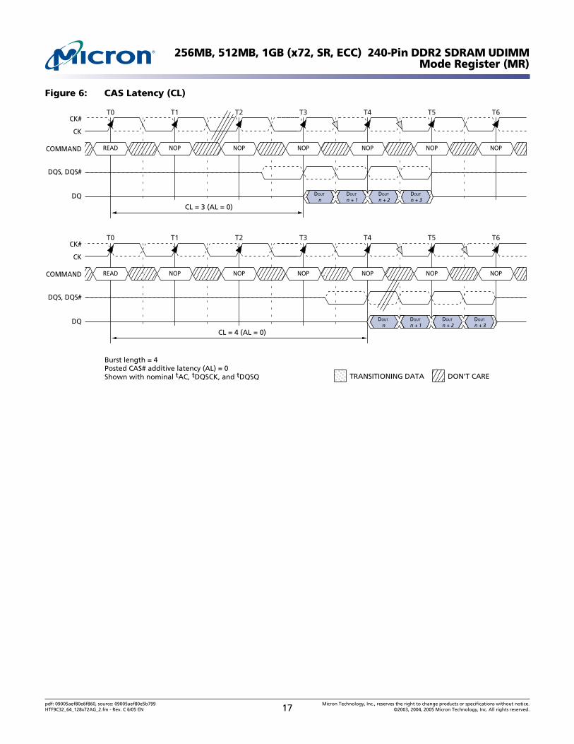
Examples of CL = 3 and CL = 4 are shown in Figure 6, CAS Latency (CL); both assume AL = 0. If a READ command is registered at clock edge n, and the CAS Latency is m clocks, the data will be available nominally coincident with clock edge n + m (this assumes AL = 0).
pdf: 09005aef80e6f860, source: 09005aef80e5b799 Micron Technology, Inc., reserves the right to change products or specifications without notice.HTF9C32_64_128x72AG_2.fm - Rev. C 6/05 EN 16 ©2003, 2004, 2005 Micron Technology, Inc. All rights reserved.
256MB, 512MB, 1GB (x72, SR, ECC) 240-Pin DDR2 SDRAM UDIMMMode Register (MR)
Figure 6: CAS Latency (CL)
DOUT
n + 3DOUT
n + 2DOUT
n + 1
CK
CK#
COMMAND
DQ
DQS, DQS#
CL = 3 (AL = 0)
READ
Burst length = 4Posted CAS# additive latency (AL) = 0Shown with nominal tAC, tDQSCK, and tDQSQ
T0 T1 T2
DON’T CARETRANSITIONING DATA
NOP NOP NOP
DOUT
n
T3 T4 T5
NOP NOP
T6
NOP
DOUT
n + 3DOUT
n + 2DOUT
n + 1
CK
CK#
COMMAND
DQ
DQS, DQS#
CL = 4 (AL = 0)
READ
T0 T1 T2
NOP NOP NOP
DOUT
n
T3 T4 T5
NOP NOP
T6
NOP
pdf: 09005aef80e6f860, source: 09005aef80e5b799 Micron Technology, Inc., reserves the right to change products or specifications without notice.HTF9C32_64_128x72AG_2.fm - Rev. C 6/05 EN 17 ©2003, 2004, 2005 Micron Technology, Inc. All rights reserved.
256MB, 512MB, 1GB (x72, SR, ECC) 240-Pin DDR2 SDRAM UDIMMExtended Mode Register (EMR)
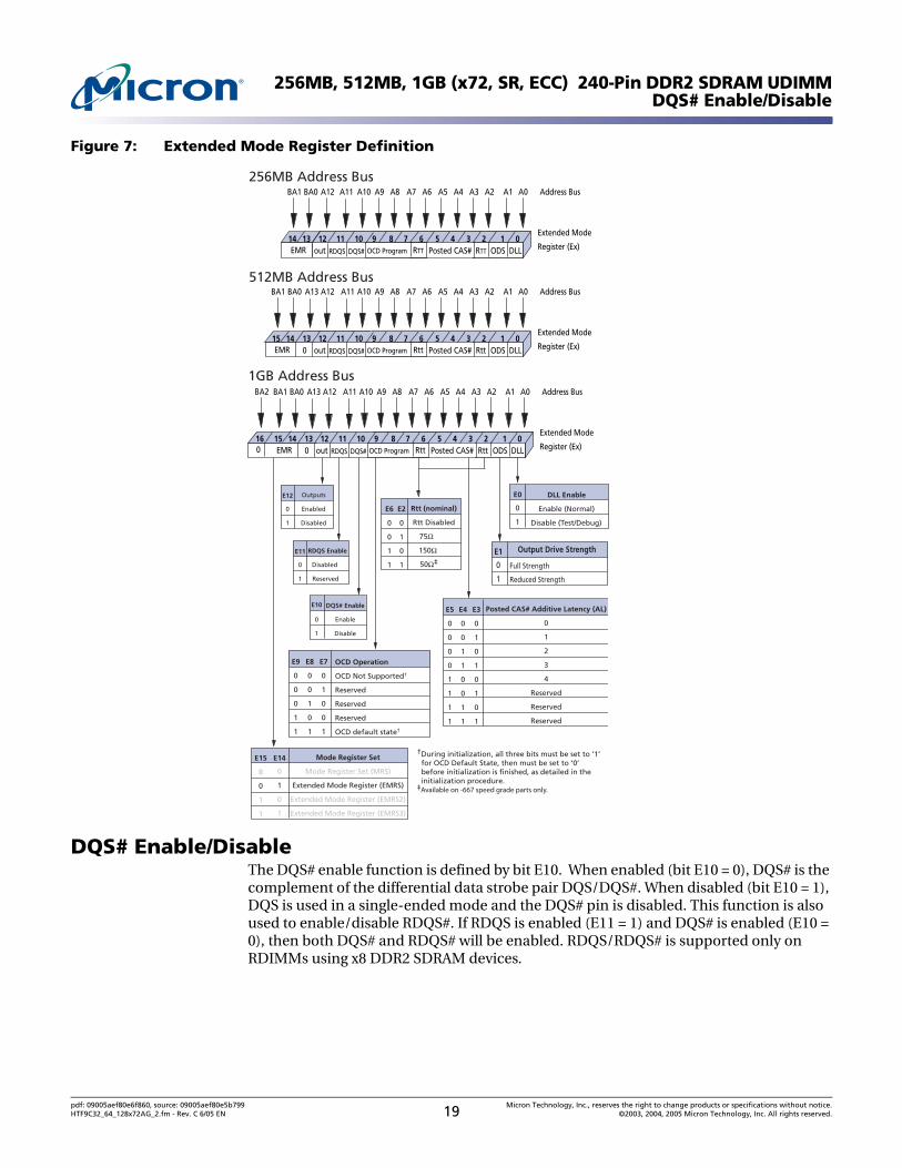
Extended Mode Register (EMR)The extended mode register controls functions beyond those controlled by the mode register; these additional functions are DLL enable/disable, output drive strength, ODT (RTT), Posted CAS additive latency (AL), off-chip driver impedance calibration (OCD), DQS# enable/disable, RDQS/RDQS# enable/disable, and OUTPUT disable/enable. These functions are controlled via the bits shown in Figure 7, Extended Mode Register Definition. The extended mode register is programmed via the LOAD MODE (LM) com-mand and will retain the stored information until it is programmed again or the device loses power. Reprogramming the extended mode register will not alter the contents of the memory array, provided it is performed correctly.
The extended mode register must be loaded when all banks are idle and no bursts are in progress, and the controller must wait the specified time tMRD before initiating any sub-sequent operation. Violating either of these requirements could result in unspecified operation.
DLL Enable/DisableThe DLL may be enabled or disabled by programming bit E0 during the LOAD MODE command as shown in Figure 7, Extended Mode Register Definition. The DLL must be enabled for normal operation. DLL enable is required during power-up initialization and upon returning to normal operation after having disabled the DLL for the purpose of debugging or evaluation. Enabling the DLL should always be followed by resetting the DLL using a LOAD MODE command.
The DLL is automatically disabled when entering self refresh operation and is automati-cally re-enabled and reset upon exit of self refresh operation.
Any time the DLL is enabled (and subsequently reset), 200 clock cycles must occur before a READ command can be issued to allow time for the internal clock to be syn-chronized with the external clock. Failing to wait for synchronization to occur may result in a violation of the tAC or tDQSCK parameters.
Output Drive StrengthThe output drive strength is defined by bit E1 as shown in Figure 7, Extended Mode Reg-ister Definition. The normal drive strength for all outputs are specified to be SSTL_18. Programming bit E1 = 0 selects normal (100 percent) drive strength for all outputs. Selecting a reduced drive strength option (bit E1 = 1) will reduce all outputs to approxi-mately 60 percent of the SSTL_18 drive strength. This option is intended for the support of the lighter load and/or point-to-point environments.
pdf: 09005aef80e6f860, source: 09005aef80e5b799 Micron Technology, Inc., reserves the right to change products or specifications without notice.HTF9C32_64_128x72AG_2.fm - Rev. C 6/05 EN 18 ©2003, 2004, 2005 Micron Technology, Inc. All rights reserved.
256MB, 512MB, 1GB (x72, SR, ECC) 240-Pin DDR2 SDRAM UDIMMDQS# Enable/Disable
Figure 7: Extended Mode Register Definition
DQS# Enable/DisableThe DQS# enable function is defined by bit E10. When enabled (bit E10 = 0), DQS# is the complement of the differential data strobe pair DQS/DQS#. When disabled (bit E10 = 1), DQS is used in a single-ended mode and the DQS# pin is disabled. This function is also used to enable/disable RDQS#. If RDQS is enabled (E11 = 1) and DQS# is enabled (E10 = 0), then both DQS# and RDQS# will be enabled. RDQS/RDQS# is supported only on RDIMMs using x8 DDR2 SDRAM devices.
DLLPosted CAS# RTTout
A9 A7 A6 A5 A4 A3A8 A2 A1 A0
Extended Mode
Register (Ex)
Address Bus
9 7 6 5 4 38 2 1 0
A10A12 A11BA0BA1
1011121314OCD Program ODSRTTDQS#RDQSEMR
DLLPosted CAS# Rttout
A9 A7 A6 A5 A4 A3A8 A2 A1 A0
Extended Mode
Register (Ex)
Address Bus
9 7 6 5 4 38 2 1 0
A10A12 A11BA0BA1
101112130
1415OCD Program
A13
ODSRttDQS#RDQSEMR
256MB Address Bus
512MB Address Bus
DLLPosted CAS# Rttout
A9 A7 A6 A5 A4 A3A8 A2 A1 A0
Extended Mode
Register (Ex)
Address Bus
9 7 6 5 4 38 2 1 0
A10A12 A11BA0BA1
101112130
1415OCD Program
A13
ODSRttDQS#RDQSEMR
BA2
160
1GB Address Bus
Posted CAS# Additive Latency (AL)
0
1
2
3
4
Reserved
Reserved
Reserved
E3
0
1
0
1
0
1
0
1
E4
0
0
1
1
0
0
1
1
E5
0
0
0
0
1
1
1
1
0
1
DLL Enable
Enable (Normal)
Disable (Test/Debug)
E0
0
1
RDQS Enable
Disabled
Reserved
E11
0
1
DQS# Enable
Enable
Disable
E10
Rtt (nominal)
Rtt Disabled
75Ω
150Ω
50Ω‡
E2
0
1
0
1
E6
0
0
1
1
0
1
Outputs
Enabled
Disabled
E12
0
1
0
1
Mode Register Set
Mode Register Set (MRS)
Extended Mode Register (EMRS)
Extended Mode Register (EMRS2)
Extended Mode Register (EMRS3)
E15
0
0
1
1
E14
OCD Operation
OCD Not Supported†
Reserved
Reserved
Reserved
OCD default state†
E7
0
1
0
0
1
E8
0
0
1
0
1
E9
0
0
0
1
1
†During initialization, all three bits must be set to ‘1’ for OCD Default State, then must be set to ‘0’ before initialization is finished, as detailed in the initialization procedure.‡Available on -667 speed grade parts only.
0
1
Output Drive StrengthE1
Full Strength
Reduced Strength
pdf: 09005aef80e6f860, source: 09005aef80e5b799 Micron Technology, Inc., reserves the right to change products or specifications without notice.HTF9C32_64_128x72AG_2.fm - Rev. C 6/05 EN 19 ©2003, 2004, 2005 Micron Technology, Inc. All rights reserved.
256MB, 512MB, 1GB (x72, SR, ECC) 240-Pin DDR2 SDRAM UDIMMRDQS Enable/Disable
RDQS Enable/DisableRDQS/RDQS# is supported only on RDIMMs using x8 DDR2 SDRAM devices. The RDQS enable function is defined by bit E11 as shown in Figure 7, Extended Mode Register Defi-nition, on page 19. When enabled (E11 = 1), RDQS is identical in function and timing to data strobe DQS during a READ. During a WRITE operation, RDQS is ignored by the DDR2 SDRAM device.
Output Enable/DisableThe OUTPUT enable function is defined by bit E12 as shown in Figure 7, Extended Mode Register Definition, on page 19. When enabled (E12 = 0), all outputs (DQs, DQS, DQS#, RDQS, RDQS#) function normally. When disabled (E12 = 1), all DDR2 SDRAM device outputs (DQs, DQS, DQS#, RDQS, RDQS#) are disabled removing output buffer current. The OUTPUT disable feature is intended to be used during IDD characterization of read current.
On Die Termination (ODT)ODT effective resistance RTT(EFF ) is defined by bits E2 and E6 of the EMR as shown in Figure 7, Extended Mode Register Definition, on page 19. The ODT feature is designed to improve signal integrity of the memory channel by allowing the DDR2 SDRAM device controller to independently turn on/off ODT for any or all devices. RTT effective resis-tance values of 75Ω and 150Ω are selectable and apply to each DQ, DQS/DQS#, RDQS/RDQS#, and DM signals. Additionally, the -667 speed modules offer a third option of 50Ω. Reserved states should not be used, as unknown operation or incompatibility with future versions may result.
The ODT control pin is used to determine when RTT(EFF ) is turned on and off, assuming ODT has been enabled via bits E2 and E6 of the EMR. The ODT feature and ODT input pin are only used during active, active power-down (both fast-exit and slow-exit modes), and precharge power-down modes of operation. If SELF REFRESH operation is used, RTT(EFF ) should always be disabled and the ODT input pin is disabled by the DDR2 SDRAM device. During power-up and initialization of the DDR2 SDRAM device, ODT should be disabled until the EMR command is issued to enable the ODT feature, at which point the ODT pin will determine the RTT(EFF ) value. Refer to the 256Mb, 512Mb, or 1Gb DDR2 SDRAM discrete data sheet for ODT timing diagrams.
Off-Chip Driver (OCD) Impedance CalibrationThe OCD function is not supported and must be set to the default state. e “Initialization” on page 11, to properly set OCD defaults.
Posted CAS Additive Latency (AL)Posted CAS additive latency (AL) is supported to make the command and data bus effi-cient for sustainable bandwidths in DDR2 SDRAM device. Bits E3–E5 define the value of AL as shown in Figure 7, Extended Mode Register Definition, on page 19. Bits E3–E5 allow the user to program the DDR2 SDRAM device with a CAS# additive latency of 0, 1, 2, 3, or 4 clocks. Reserved states should not be used as unknown operation or incompat-ibility with future versions may result.
In this operation, the DDR2 SDRAM device allows a READ or WRITE command to be issued prior to tRCD (MIN) with the requirement that AL ≤ tRCD(MIN). A typical appli-cation using this feature would set AL = tRCD (MIN) - 1 x tCK. The READ or WRITE com-mand is held for the time of the additive latency (AL) before it is issued internally to the DDR2 SDRAM device. READ Latency (RL) is controlled by the sum of the Posted CAS
pdf: 09005aef80e6f860, source: 09005aef80e5b799 Micron Technology, Inc., reserves the right to change products or specifications without notice.HTF9C32_64_128x72AG_2.fm - Rev. C 6/05 EN 20 ©2003, 2004, 2005 Micron Technology, Inc. All rights reserved.
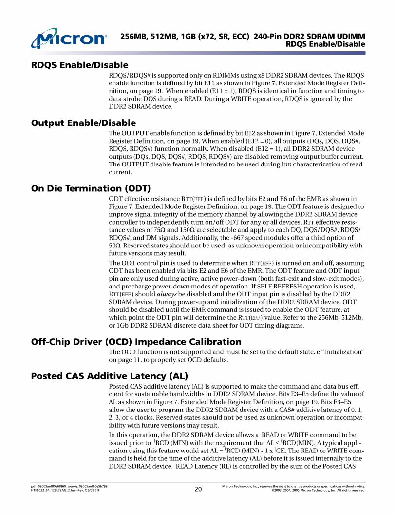
256MB, 512MB, 1GB (x72, SR, ECC) 240-Pin DDR2 SDRAM UDIMMPosted CAS Additive Latency (AL)
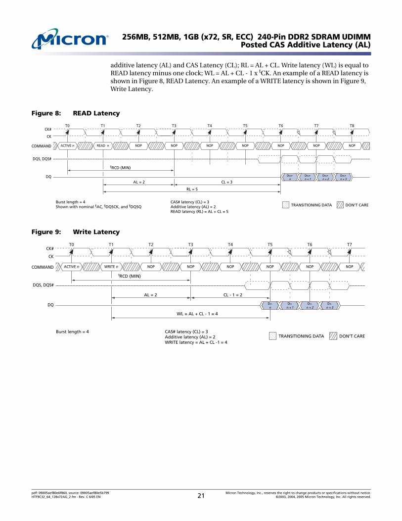
additive latency (AL) and CAS Latency (CL); RL = AL + CL. Write latency (WL) is equal to READ latency minus one clock; WL = AL + CL - 1 x tCK. An example of a READ latency is shown in Figure 8, READ Latency. An example of a WRITE latency is shown in Figure 9, Write Latency.
Figure 8: READ Latency
Figure 9: Write Latency
DOUT
n + 3DOUT
n + 2DOUT
n + 1
CK
CK#
COMMAND
DQ
DQS, DQS#
AL = 2
ACTIVE n
Burst length = 4 Shown with nominal tAC, tDQSCK, and tDQSQ
T0 T1 T2
DON’T CARETRANSITIONING DATA
READ n NOP NOP
DOUT
n
T3 T4 T5
NOP
T6
NOP
T7 T8
NOP NOP
CL = 3
RL = 5
CAS# latency (CL) = 3Additive latency (AL) = 2READ latency (RL) = AL + CL = 5
tRCD (MIN)
NOP
CK
CK#
COMMAND
DQ
DQS, DQS#
ACTIVE n
Burst length = 4
T0 T1 T2
DON’T CARETRANSITIONING DATA
NOP NOP
T3 T4 T5
NOPWRITE n
T6
NOP
Din
n + 3Din
n + 2Din
n + 1
WL = AL + CL - 1 = 4
T7
NOP
Din
n
CAS# latency (CL) = 3Additive latency (AL) = 2WRITE latency = AL + CL -1 = 4
tRCD (MIN)
NOP
AL = 2 CL - 1 = 2
pdf: 09005aef80e6f860, source: 09005aef80e5b799 Micron Technology, Inc., reserves the right to change products or specifications without notice.HTF9C32_64_128x72AG_2.fm - Rev. C 6/05 EN 21 ©2003, 2004, 2005 Micron Technology, Inc. All rights reserved.
256MB, 512MB, 1GB (x72, SR, ECC) 240-Pin DDR2 SDRAM UDIMMExtended Mode Register 2 (EMR2)
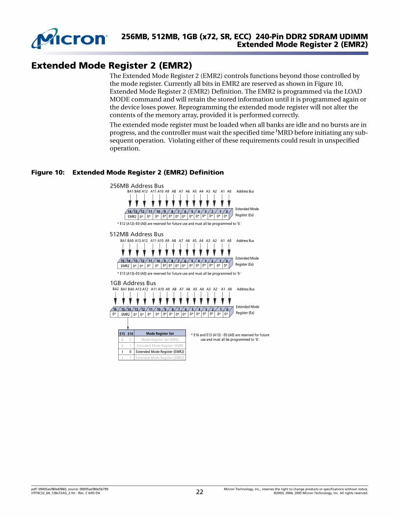
Extended Mode Register 2 (EMR2)The Extended Mode Register 2 (EMR2) controls functions beyond those controlled by the mode register. Currently all bits in EMR2 are reserved as shown in Figure 10, Extended Mode Register 2 (EMR2) Definition. The EMR2 is programmed via the LOAD MODE command and will retain the stored information until it is programmed again or the device loses power. Reprogramming the extended mode register will not alter the contents of the memory array, provided it is performed correctly.
The extended mode register must be loaded when all banks are idle and no bursts are in progress, and the controller must wait the specified time tMRD before initiating any sub-sequent operation. Violating either of these requirements could result in unspecified operation.
Figure 10: Extended Mode Register 2 (EMR2) Definition
A9 A7 A6 A5 A4 A3A8 A2 A1 A0
Extended Mode
Register (Ex)
Address Bus
9 7 6 5 4 38 2 1 0
A10A12 A11BA0BA1
10111213
* E12 (A12)–E0 (A0) are reserved for future use and must all be programmed to '0.'
14EMR2 0* 0* 0* 0* 0* 0* 0* 0* 0* 0* 0* 0* 0*
A9 A7 A6 A5 A4 A3A8 A2 A1 A0
Extended Mode
Register (Ex)
Address Bus
9 7 6 5 4 38 2 1 0
A10A12 A11BA0BA1
101112130*
1415
A13
EMR2 0* 0* 0* 0* 0* 0* 0* 0* 0* 0* 0* 0* 0*
256MB Address Bus
512MB Address Bus
A9 A7 A6 A5 A4 A3A8 A2 A1 A0
Extended Mode
Register (Ex)
Address Bus
9 7 6 5 4 38 2 1 0
A10A12 A11BA0BA1
101112130*
14
* E16 and E13 (A13) - E0 (A0) are reserved for futureuse and must all be programmed to '0'.
15
A13
0
1
0
1
Mode Register Set
Mode Register Set (MRS)
Extended Mode Register (EMR)
Extended Mode Register (EMR2)
Extended Mode Register (EMR3)
E15
0
0
1
1
E14
EMR2 0* 0* 0* 0* 0* 0* 0* 0* 0* 0* 0* 0* 0*
BA2
160*
1GB Address Bus
* E13 (A13)–E0 (A0) are reserved for future use and must all be programmed to '0.'
pdf: 09005aef80e6f860, source: 09005aef80e5b799 Micron Technology, Inc., reserves the right to change products or specifications without notice.HTF9C32_64_128x72AG_2.fm - Rev. C 6/05 EN 22 ©2003, 2004, 2005 Micron Technology, Inc. All rights reserved.

256MB, 512MB, 1GB (x72, SR, ECC) 240-Pin DDR2 SDRAM UDIMMExtended Mode Register 3 (EMR3)
Extended Mode Register 3 (EMR3)The Extended Mode Register 3 (EMR3) controls functions beyond those controlled by the mode register. Currently all bits in EMR3 are reserved as shown in Figure 11, Extended Mode Register 3 (EMR3) Definition. The EMR3 is programmed via the LOAD MODE command and will retain the stored information until it is programmed again or the device loses power. Reprogramming the extended mode register will not alter the contents of the memory array, provided it is performed correctly.
The extended mode register must be loaded when all banks are idle and no bursts are in progress, and the controller must wait the specified time tMRD before initiating any sub-sequent operation. Violating either of these requirements could result in unspecified operation.
Figure 11: Extended Mode Register 3 (EMR3) Definition
A9 A7 A6 A5 A4 A3A8 A2 A1 A0
Extended Mode
Register (Ex)
Address Bus
9 7 6 5 4 38 2 1 0
A10A12 A11BA0BA1
10111213
* E12 (A12)–E0 (A0) are reserved for future use and must all be programmed to '0.'
14EMR3 0* 0* 0* 0* 0* 0* 0* 0* 0* 0* 0* 0* 0*
A9 A7 A6 A5 A4 A3A8 A2 A1 A0
Extended Mode
Register (Ex)
Address Bus
9 7 6 5 4 38 2 1 0
A10A12 A11BA0BA1
101112130*
1415
A13
EMR3 0* 0* 0* 0* 0* 0* 0* 0* 0* 0* 0* 0* 0*
256MB Address Bus
512MB Address Bus
A9 A7 A6 A5 A4 A3A8 A2 A1 A0
Extended Mode
Register (Ex)
Address Bus
9 7 6 5 4 38 2 1 0
A10A12 A11BA0BA1
101112130*
1415
A13
0
1
0
1
Mode Register Set
Mode Register Set (MRS)
Extended Mode Register (EMR)
Extended Mode Register (EMR2)
Extended Mode Register (EMR3)
E15
0
0
1
1
E14
EMR3 0* 0* 0* 0* 0* 0* 0* 0* 0* 0* 0* 0* 0*
* E16 and E13 (A13) - E0 (A0) are reserved for futureuse and must all be programmed to '0'.
BA2
160*
* E13 (A13)–E0 (A0) are reserved for future use and must all be programmed to '0.'
1GB Address Bus
pdf: 09005aef80e6f860, source: 09005aef80e5b799 Micron Technology, Inc., reserves the right to change products or specifications without notice.HTF9C32_64_128x72AG_2.fm - Rev. C 6/05 EN 23 ©2003, 2004, 2005 Micron Technology, Inc. All rights reserved.
256MB, 512MB, 1GB (x72, SR, ECC) 240-Pin DDR2 SDRAM UDIMMCommand Truth Tables
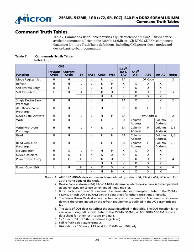
Command Truth TablesTable 7, Commands Truth Table provides a quick reference of DDR2 SDRAM device available commands. Refer to the 256Mb, 512Mb, or 1Gb DDR2 SDRAM component data sheet for more Truth Table definitions, including CKE power-down modes and device bank-to-bank commands.
Notes: 1. All DDR2 SDRAM device commands are defined by states of S#, RAS#, CAS#, WE#, and CKE at the rising edge of the clock.
2. Device Bank addresses (BA) BA0–BA1/BA2 determine which device bank is to be operated upon. For EMR, BA selects an extended mode register.
3. Burst reads or writes at BL = 4 cannot be terminated or interrupted. Refer to the 256Mb, 512Mb, or 1Gb DDR2 SDRAM discrete data sheet for other restrictions or details.
4. The Power Down Mode does not perform any refresh operations. The duration of power-down is therefore limited by the refresh requirements outlined in the AC parametric sec-tion.
5. The state of ODT does not affect the states described in this table. The ODT function is not available during self refresh. Refer to the 256Mb, 512Mb, or 1Gb DDR2 SDRAM discrete data sheet for other restrictions or details.
6. “X” means “H or L” (but a defined logic level).7. Self refresh exit is asynchronous.8. BA2 valid for 1GB only; A13 valid for 512MB and 1GB only.
Table 7: Commands Truth TableNotes: 1, 5, 6
Function
CKE
S# RAS# CAS# WE#
BA28, BA1,BA0
A138–A11 A10 A9–A0 Notes
Previous Cycle
Current Cycle
Mode Register Set H H L L L L BA OP Code 2
Refresh H H L L L H X X X X
Self Refresh Entry H L L L L H X X X X
Self Refresh Exit L H X X X X X X X X 7L H H H X X X X
Single Device Bank Precharge
H H L L H L BA X L X 2
ALL Device Banks Precharge
H H L L H L X X H X
Device Bank Activate H H L L H H BA Row Address 2
Write H H L H L L BA Column Address
L Column Address
2, 3
Write with Auto Precharge
H H L H L L BA Column Address
H Column Address
2, 3
Read H H L H L H BA Column Address
L Column Address
2, 3
Read with Auto Precharge
H H L H L H BA Column Address
H Column Address
2, 3
No Operation H X L H H H X X X X
Device Deselect H X H X X X X X X X
Power-Down Entry H L H X X X X X X X 4L H H H X X X X
Power-Down Exit L H H X X X X X X X 4L H H H X X X X
pdf: 09005aef80e6f860, source: 09005aef80e5b799 Micron Technology, Inc., reserves the right to change products or specifications without notice.HTF9C32_64_128x72AG_2.fm - Rev. C 6/05 EN 24 ©2003, 2004, 2005 Micron Technology, Inc. All rights reserved.
256MB, 512MB, 1GB (x72, SR, ECC) 240-Pin DDR2 SDRAM UDIMMAbsolute Maximum Ratings
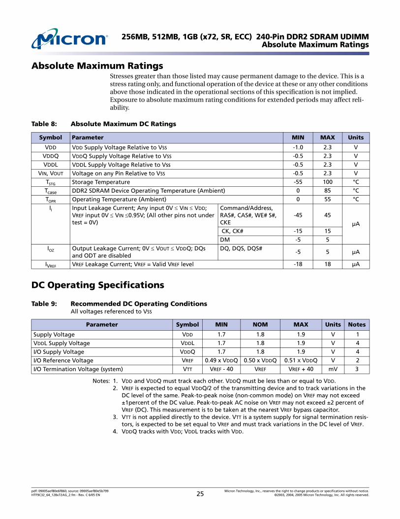
Absolute Maximum RatingsStresses greater than those listed may cause permanent damage to the device. This is a stress rating only, and functional operation of the device at these or any other conditions above those indicated in the operational sections of this specification is not implied. Exposure to absolute maximum rating conditions for extended periods may affect reli-ability.
DC Operating Specifications
Notes: 1. VDD and VDDQ must track each other. VDDQ must be less than or equal to VDD.2. VREF is expected to equal VDDQ/2 of the transmitting device and to track variations in the
DC level of the same. Peak-to-peak noise (non-common mode) on VREF may not exceed ±1percent of the DC value. Peak-to-peak AC noise on VREF may not exceed ±2 percent of VREF (DC). This measurement is to be taken at the nearest VREF bypass capacitor.
3. VTT is not applied directly to the device. VTT is a system supply for signal termination resis-tors, is expected to be set equal to VREF and must track variations in the DC level of VREF.
4. VDDQ tracks with VDD; VDDL tracks with VDD.
Table 8: Absolute Maximum DC Ratings
Symbol Parameter MIN MAX Units
VDD VDD Supply Voltage Relative to VSS -1.0 2.3 VVDDQ VDDQ Supply Voltage Relative to VSS -0.5 2.3 VVDDL VDDL Supply Voltage Relative to Vss -0.5 2.3 V
VIN, VOUT Voltage on any Pin Relative to VSS -0.5 2.3 VTSTG Storage Temperature -55 100 °CTcase DDR2 SDRAM Device Operating Temperature (Ambient) 0 85 °CTOPR Operating Temperature (Ambient) 0 55 °C
II Input Leakage Current; Any input 0V ≤ VIN ≤ VDD; VREF input 0V ≤ VIN ≤0.95V; (All other pins not under test = 0V)
Command/Address, RAS#, CAS#, WE# S#, CKE
-45 45µA
CK, CK# -15 15DM -5 5
IOZ Output Leakage Current; 0V ≤ VOUT ≤ VDDQ; DQs and ODT are disabled
DQ, DQS, DQS#-5 5 µA
IVREF VREF Leakage Current; VREF = Valid VREF level -18 18 µA
Table 9: Recommended DC Operating ConditionsAll voltages referenced to VSS
Parameter Symbol MIN NOM MAX Units Notes
Supply Voltage VDD 1.7 1.8 1.9 V 1
VDDL Supply Voltage VDDL 1.7 1.8 1.9 V 4
I/O Supply Voltage VDDQ 1.7 1.8 1.9 V 4
I/O Reference Voltage VREF 0.49 x VDDQ 0.50 x VDDQ 0.51 X VDDQ V 2
I/O Termination Voltage (system) VTT VREF - 40 VREF VREF + 40 mV 3
pdf: 09005aef80e6f860, source: 09005aef80e5b799 Micron Technology, Inc., reserves the right to change products or specifications without notice.HTF9C32_64_128x72AG_2.fm - Rev. C 6/05 EN 25 ©2003, 2004, 2005 Micron Technology, Inc. All rights reserved.
256MB, 512MB, 1GB (x72, SR, ECC) 240-Pin DDR2 SDRAM UDIMMInput Electrical Characteristics and Operating Conditions
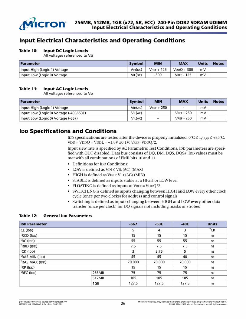
Input Electrical Characteristics and Operating Conditions
IDD Specifications and ConditionsIDD specifications are tested after the device is properly initialized. 0°C ≤ TCASE ≤ +85°C. VDD = VDDQ = VDDL = +1.8V ±0.1V; VREF=VDDQ/2.
Input slew rate is specified by AC Parametric Test Conditions. IDD parameters are speci-fied with ODT disabled. Data bus consists of DQ, DM, DQS, DQS#. IDD values must be met with all combinations of EMR bits 10 and 11.
• Definitions for IDD Conditions: • LOW is defined as VIN ≤ VIL (AC) (MAX)• HIGH is defined as VIN ≥ VIH (AC) (MIN)• STABLE is defined as inputs stable at a HIGH or LOW level• FLOATING is defined as inputs at VREF = VDDQ/2• SWITCHING is defined as inputs changing between HIGH and LOW every other clock
cycle (once per two clocks) for address and control signals• Switching is defined as inputs changing between HIGH and LOW every other data
transfer (once per clock) for DQ signals not including masks or strobes
Table 10: Input DC Logic LevelsAll voltages referenced to VSS
Parameter Symbol MIN MAX Units Notes
Input High (Logic 1) Voltage VIH(DC) VREF + 125 VDDQ + 300 mV
Input Low (Logic 0) Voltage VIL(DC) -300 VREF - 125 mV
Table 11: Input AC Logic LevelsAll voltages referenced to VSS
Parameter Symbol MIN MAX Units Notes
Input High (Logic 1) Voltage VIH(AC) VREF + 250 - mV
Input Low (Logic 0) Voltage (-40E/-53E) VIL(AC) – VREF - 250 mV
Input Low (Logic 0) Voltage (-667) VIL(AC) – VREF - 250 mV
Table 12: General IDD Parameters
IDD Parameter -667 -53E -40E Units
CL (IDD) 5 4 3 tCKtRCD (IDD) 15 15 15 nstRC (IDD) 55 55 55 nstRRD (IDD) 7.5 7.5 7.5 nstCK (IDD) 3 3.75 5 nstRAS MIN (IDD) 45 45 40 nstRAS MAX (IDD) 70,000 70,000 70,000 nstRP (IDD) 15 15 15 nstRFC (IDD) 256MB 75 75 75 ns
512MB 105 105 105 ns
1GB 127.5 127.5 127.5 ns
pdf: 09005aef80e6f860, source: 09005aef80e5b799 Micron Technology, Inc., reserves the right to change products or specifications without notice.HTF9C32_64_128x72AG_2.fm - Rev. C 6/05 EN 26 ©2003, 2004, 2005 Micron Technology, Inc. All rights reserved.
256MB, 512MB, 1GB (x72, SR, ECC) 240-Pin DDR2 SDRAM UDIMMIDD Specifications and Conditions
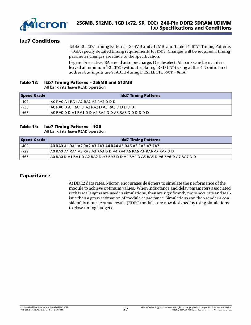
IDD7 ConditionsTable 13, IDD7 Timing Patterns – 256MB and 512MB, and Table 14, IDD7 Timing Patterns – 1GB, specify detailed timing requirements for IDD7. Changes will be required if timing parameter changes are made to the specification.
Legend: A = active; RA = read auto precharge; D = deselect. All banks are being inter-leaved at minimum tRC (IDD) without violating tRRD (IDD) using a BL = 4. Control and address bus inputs are STABLE during DESELECTs. IOUT = 0mA.
CapacitanceAt DDR2 data rates, Micron encourages designers to simulate the performance of the module to achieve optimum values. When inductance and delay parameters associated with trace lengths are used in simulations, they are significantly more accurate and real-istic than a gross estimation of module capacitance. Simulations can then render a con-siderably more accurate result. JEDEC modules are now designed by using simulations to close timing budgets.
Table 13: IDD7 Timing Patterns – 256MB and 512MBAll bank interleave READ operation
Speed Grade Idd7 Timing Patterns
-40E A0 RA0 A1 RA1 A2 RA2 A3 RA3 D D D -53E A0 RA0 D A1 RA1 D A2 RA2 D A3 RA3 D D D D D-667 A0 RA0 D D A1 RA1 D D A2 RA2 D D A3 RA3 D D D D D D
Table 14: IDD7 Timing Patterns – 1GBAll bank interleave READ operation
Speed Grade Idd7 Timing Patterns
-40E A0 RA0 A1 RA1 A2 RA2 A3 RA3 A4 RA4 A5 RA5 A6 RA6 A7 RA7-53E A0 RA0 A1 RA1 A2 RA2 A3 RA3 D D A4 RA4 A5 RA5 A6 RA6 A7 RA7 D D-667 A0 RA0 D A1 RA1 D A2 RA2 D A3 RA3 D D A4 RA4 D A5 RA5 D A6 RA6 D A7 RA7 D D
pdf: 09005aef80e6f860, source: 09005aef80e5b799 Micron Technology, Inc., reserves the right to change products or specifications without notice.HTF9C32_64_128x72AG_2.fm - Rev. C 6/05 EN 27 ©2003, 2004, 2005 Micron Technology, Inc. All rights reserved.
256MB, 512MB, 1GB (x72, SR, ECC) 240-Pin DDR2 SDRAM UDIMMIDD Specifications and Conditions
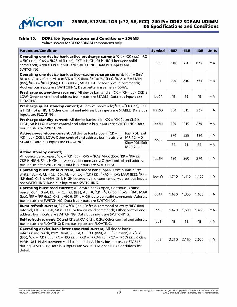
Table 15: DDR2 IDD Specifications and Conditions – 256MBValues shown for DDR2 SDRAM components only
Parameter/Condition Symbol -667 -53E -40E Units
Operating one device bank active-precharge current; tCK = tCK (IDD), tRC = tRC (IDD), tRAS = tRAS MIN (IDD); CKE is HIGH, S# is HIGH between valid commands; Address bus inputs are SWITCHING; Data bus inputs are SWITCHING.
IDD0 810 720 675 mA
Operating one device bank active-read-precharge current; IOUT = 0mA; BL = 4, CL = CL(IDD), AL = 0; tCK = tCK (IDD), tRC = tRC (IDD), tRAS = tRAS MIN (IDD), tRCD = tRCD (IDD); CKE is HIGH, S# is HIGH between valid commands; Address bus inputs are SWITCHING; Data pattern is same as IDD4W.
IDD1 900 810 765 mA
Precharge power-down current; All device banks idle; tCK = tCK (IDD); CKE is LOW; Other control and address bus inputs are STABLE; Data bus inputs are FLOATING.
IDD2P 45 45 45 mA
Precharge quiet standby current; All device banks idle; tCK = tCK (IDD); CKE is HIGH, S# is HIGH; Other control and address bus inputs are STABLE; Data bus inputs are FLOATING.
IDD2Q 360 315 225 mA
Precharge standby current; All device banks idle; tCK = tCK (IDD); CKE is HIGH, S# is HIGH; Other control and address bus inputs are SWITCHING; Data bus inputs are SWITCHING.
IDD2N 360 315 270 mA
Active power-down current; All device banks open; tCK = tCK (IDD); CKE is LOW; Other control and address bus inputs are STABLE; Data bus inputs are FLOATING.
Fast PDN Exit MR[12] = 0
IDD3P270 225 180 mA
Slow PDN Exit MR[12] = 1
54 54 54 mA
Active standby current;All device banks open; tCK = tCK(IDD), tRAS = tRAS MAX (IDD), tRP = tRP(IDD); CKE is HIGH, S# is HIGH between valid commands; Other control and address bus inputs are SWITCHING; Data bus inputs are SWITCHING.
IDD3N 450 360 270 mA
Operating burst write current; All device banks open, Continuous burst writes; BL = 4, CL = CL (IDD), AL = 0; tCK = tCK (IDD), tRAS = tRAS MAX (IDD), tRP = tRP (IDD); CKE is HIGH, S# is HIGH between valid commands; Address bus inputs are SWITCHING; Data bus inputs are SWITCHING.
IDD4W 1,710 1,440 1,125 mA
Operating burst read current; All device banks open, Continuous burst reads, IOUT = 0mA; BL = 4, CL = CL (IDD), AL = 0; tCK = tCK (IDD), tRAS = tRAS MAX (IDD), tRP = tRP (IDD); CKE is HIGH, S# is HIGH between valid commands; Address bus inputs are SWITCHING; Data bus inputs are SWITCHING.
IDD4R 1,620 1,350 1,035 mA
Burst refresh current; tCK = tCK (IDD); Refresh command at every tRFC (IDD) interval; CKE is HIGH, S# is HIGH between valid commands; Other control and address bus inputs are SWITCHING; Data bus inputs are SWITCHING.
IDD5 1,620 1,530 1,485 mA
Self refresh current; CK and CK# at 0V; CKE ≤ 0.2V; Other control and address bus inputs are FLOATING; Data bus inputs are FLOATING.
IDD6 45 45 45 mA
Operating device bank interleave read current; All device banks interleaving reads, IOUT= 0mA; BL = 4, CL = CL (IDD), AL = tRCD (IDD)-1 x tCK (IDD); tCK = tCK (IDD), tRC = tRC(IDD), tRRD = tRRD(IDD), tRCD = tRCD(IDD); CKE is HIGH, S# is HIGH between valid commands; Address bus inputs are STABLE during DESELECTs; Data bus inputs are SWITCHING; See IDD7 Conditions for detail.
IDD7 2,250 2,160 2,070 mA
pdf: 09005aef80e6f860, source: 09005aef80e5b799 Micron Technology, Inc., reserves the right to change products or specifications without notice.HTF9C32_64_128x72AG_2.fm - Rev. C 6/05 EN 28 ©2003, 2004, 2005 Micron Technology, Inc. All rights reserved.

256MB, 512MB, 1GB (x72, SR, ECC) 240-Pin DDR2 SDRAM UDIMMIDD Specifications and Conditions
Table 16: DDR2 IDD Specifications and Conditions – 512MBValues shown for DDR2 SDRAM components only
Parameter/Condition Symbol -667 -53E -40E Units
Operating one device bank active-precharge current; tCK = tCK (IDD), tRC = tRC (IDD), tRAS = tRAS MIN (IDD); CKE is HIGH, S# is HIGH between valid commands; Address bus inputs are SWITCHING; Data bus inputs are SWITCHING.
IDD0 810 720 720 mA
Operating one device bank active-read-precharge current; IOUT = 0mA; BL = 4, CL = CL(IDD), AL = 0; tCK = tCK (IDD), tRC = tRC (IDD), tRAS = tRAS MIN (IDD), tRCD = tRCD (IDD); CKE is HIGH, S# is HIGH between valid commands; Address bus inputs are SWITCHING; Data pattern is same as IDD4W.
IDD1 945 855 810 mA
Precharge power-down current; All device banks idle; tCK = tCK (IDD); CKE is LOW; Other control and address bus inputs are STABLE; Data bus inputs are FLOATING.
IDD2P 45 45 45 mA
Precharge quiet standby current; All device banks idle; tCK = tCK (IDD); CKE is HIGH, S# is HIGH; Other control and address bus inputs are STABLE; Data bus inputs are FLOATING.
IDD2Q 450 360 315 mA
Precharge standby current; All device banks idle; tCK = tCK (IDD); CKE is HIGH, S# is HIGH; Other control and address bus inputs are SWITCHING; Data bus inputs are SWITCHING.
IDD2N 495 405 360 mA
Active power-down current; All device banks open; tCK = tCK (IDD); CKE is LOW; Other control and address bus inputs are STABLE; Data bus inputs are FLOATING.
Fast PDN Exit MR[12] = 0
IDD3P315 270 225 mA
Slow PDN Exit MR[12] = 1
90 90 90 mA
Active standby current;All device banks open; tCK = tCK(IDD), tRAS = tRAS MAX (IDD), tRP = tRP(IDD); CKE is HIGH, S# is HIGH between valid commands; Other control and address bus inputs are SWITCHING; Data bus inputs are SWITCHING.
IDD3N 585 495 405 mA
Operating burst write current; All device banks open, Continuous burst writes; BL = 4, CL = CL (IDD), AL = 0; tCK = tCK (IDD), tRAS = tRAS MAX (IDD), tRP = tRP (IDD); CKE is HIGH, S# is HIGH between valid commands; Address bus inputs are SWITCHING; Data bus inputs are SWITCHING.
IDD4W 1,395 1,170 990 mA
Operating burst read current; All device banks open, Continuous burst reads, IOUT = 0mA; BL = 4, CL = CL (IDD), AL = 0; tCK = tCK (IDD), tRAS = tRAS MAX (IDD), tRP = tRP (IDD); CKE is HIGH, S# is HIGH between valid commands; Address bus inputs are SWITCHING; Data bus inputs are SWITCHING.
IDD4R 1,575 1,305 1,035 mA
Burst refresh current; tCK = tCK (IDD); Refresh command at every tRFC (IDD) interval; CKE is HIGH, S# is HIGH between valid commands; Other control and address bus inputs are SWITCHING; Data bus inputs are SWITCHING.
IDD5 1,890 1,800 1,710 mA
Self refresh current; CK and CK# at 0V; CKE ≤ 0.2V; Other control and address bus inputs are FLOATING; Data bus inputs are FLOATING.
IDD6 45 45 45 mA
Operating device bank interleave read current; All device banks interleaving reads, IOUT= 0mA; BL = 4, CL = CL (IDD), AL = tRCD (IDD)-1 x tCK (IDD); tCK = tCK (IDD), tRC = tRC(IDD), tRRD = tRRD(IDD), tRCD = tRCD(IDD); CKE is HIGH, S# is HIGH between valid commands; Address bus inputs are STABLE during DESELECTs; Data bus inputs are SWITCHING; See IDD7 Conditions for detail.
IDD7 2,520 2,340 2,070 mA
pdf: 09005aef80e6f860, source: 09005aef80e5b799 Micron Technology, Inc., reserves the right to change products or specifications without notice.HTF9C32_64_128x72AG_2.fm - Rev. C 6/05 EN 29 ©2003, 2004, 2005 Micron Technology, Inc. All rights reserved.

256MB, 512MB, 1GB (x72, SR, ECC) 240-Pin DDR2 SDRAM UDIMMIDD Specifications and Conditions
Table 17: DDR2 IDD Specifications and Conditions – 1GBValues shown for DDR2 SDRAM components only
Parameter/Condition Symbol -667 -53E -40E Units
Operating one device bank active-precharge current; tCK = tCK (IDD), tRC = tRC (IDD), tRAS = tRAS MIN (IDD); CKE is HIGH, S# is HIGH between valid commands; Address bus inputs are SWITCHING; Data bus inputs are SWITCHING.
IDD0 900 720 720 mA
Operating one device bank active-read-precharge current; IOUT = 0mA; BL = 4, CL = CL(IDD), AL = 0; tCK = tCK (IDD), tRC = tRC (IDD), tRAS = tRAS MIN (IDD), tRCD = tRCD (IDD); CKE is HIGH, S# is HIGH between valid commands; Address bus inputs are SWITCHING; Data pattern is same as IDD4W.
IDD1 1,305 855 855 mA
Precharge power-down current; All device banks idle; tCK = tCK (IDD); CKE is LOW; Other control and address bus inputs are STABLE; Data bus inputs are FLOATING.
IDD2P 63 45 45 mA
Precharge quiet standby current; All device banks idle; tCK = tCK (IDD); CKE is HIGH, S# is HIGH; Other control and address bus inputs are STABLE; Data bus inputs are FLOATING.
IDD2Q 540 369 315 mA
Precharge standby current; All device banks idle; tCK = tCK (IDD); CKE is HIGH, S# is HIGH; Other control and address bus inputs are SWITCHING; Data bus inputs are SWITCHING.
IDD2N 585 405 315 mA
Active power-down current; All device banks open; tCK = tCK (IDD); CKE is LOW; Other control and address bus inputs are STABLE; Data bus inputs are FLOATING.
Fast PDN Exit MR[12] = 0
IDD3P360 270 225 mA
Slow PDN Exit MR[12] = 1
45 45 45 mA
Active standby current;All device banks open; tCK = tCK(IDD), tRAS = tRAS MAX (IDD), tRP = tRP(IDD); CKE is HIGH, S# is HIGH between valid commands; Other control and address bus inputs are SWITCHING; Data bus inputs are SWITCHING.
IDD3N 630 450 360 mA
Operating burst write current; All device banks open, Continuous burst writes; BL = 4, CL = CL (IDD), AL = 0; tCK = tCK (IDD), tRAS = tRAS MAX (IDD), tRP = tRP (IDD); CKE is HIGH, S# is HIGH between valid commands; Address bus inputs are SWITCHING; Data bus inputs are SWITCHING.
IDD4W 1,620 1,170 1,080 mA
Operating burst read current; All device banks open, Continuous burst reads, IOUT = 0mA; BL = 4, CL = CL (IDD), AL = 0; tCK = tCK (IDD), tRAS = tRAS MAX (IDD), tRP = tRP (IDD); CKE is HIGH, S# is HIGH between valid commands; Address bus inputs are SWITCHING; Data bus inputs are SWITCHING.
IDD4R 1,845 1,305 1,215 mA
Burst refresh current; tCK = tCK (IDD); Refresh command at every tRFC (IDD) interval; CKE is HIGH, S# is HIGH between valid commands; Other control and address bus inputs are SWITCHING; Data bus inputs are SWITCHING.
IDD5 2,430 2,250 2,160 mA
Self refresh current; CK and CK# at 0V; CKE ≤ 0.2V; Other control and address bus inputs are FLOATING; Data bus inputs are FLOATING.
IDD6 63 45 45 mA
Operating device bank interleave read current; All device banks interleaving reads, IOUT= 0mA; BL = 4, CL = CL (IDD), AL = tRCD (IDD)-1 x tCK (IDD); tCK = tCK (IDD), tRC = tRC(IDD), tRRD = tRRD(IDD), tRCD = tRCD(IDD); CKE is HIGH, S# is HIGH between valid commands; Address bus inputs are STABLE during DESELECTs; Data bus inputs are SWITCHING; See IDD7 Conditions for detail.
IDD7 3,060 2,655 2,655 mA
pdf: 09005aef80e6f860, source: 09005aef80e5b799 Micron Technology, Inc., reserves the right to change products or specifications without notice.HTF9C32_64_128x72AG_2.fm - Rev. C 6/05 EN 30 ©2003, 2004, 2005 Micron Technology, Inc. All rights reserved.
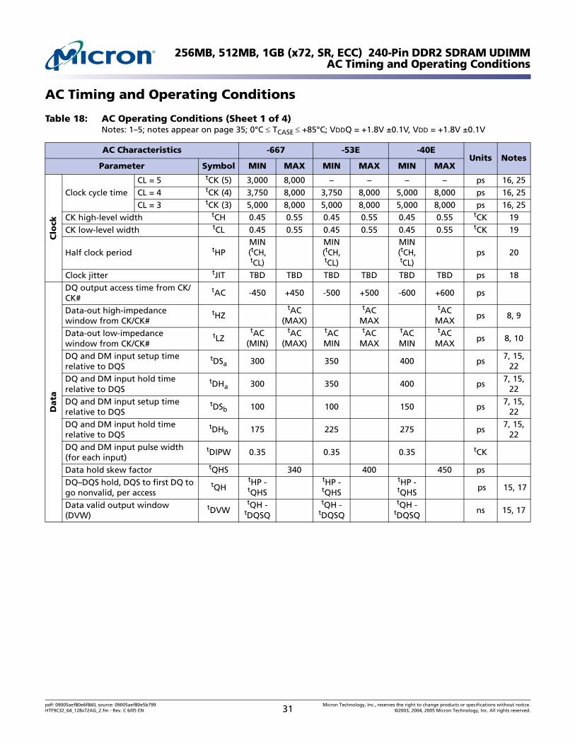
256MB, 512MB, 1GB (x72, SR, ECC) 240-Pin DDR2 SDRAM UDIMMAC Timing and Operating Conditions
AC Timing and Operating Conditions
Table 18: AC Operating Conditions (Sheet 1 of 4)Notes: 1–5; notes appear on page 35; 0°C ≤ TCASE ≤ +85°C; VDDQ = +1.8V ±0.1V, VDD = +1.8V ±0.1V
AC Characteristics -667 -53E -40EUnits Notes
Parameter Symbol MIN MAX MIN MAX MIN MAX
Clo
ck
Clock cycle timeCL = 5 tCK (5) 3,000 8,000 – – – – ps 16, 25CL = 4 tCK (4) 3,750 8,000 3,750 8,000 5,000 8,000 ps 16, 25CL = 3 tCK (3) 5,000 8,000 5,000 8,000 5,000 8,000 ps 16, 25
CK high-level width tCH 0.45 0.55 0.45 0.55 0.45 0.55 tCK 19CK low-level width tCL 0.45 0.55 0.45 0.55 0.45 0.55 tCK 19
Half clock period tHPMIN (tCH, tCL)
MIN (tCH, tCL)
MIN (tCH, tCL)
ps 20
Clock jitter tJIT TBD TBD TBD TBD TBD TBD ps 18
Da
ta
DQ output access time from CK/CK#
tAC -450 +450 -500 +500 -600 +600 ps
Data-out high-impedance window from CK/CK#
tHZtAC
(MAX)
tAC MAX
tAC MAX
ps 8, 9
Data-out low-impedance window from CK/CK#
tLZtAC
(MIN)
tAC (MAX)
tAC MIN
tAC MAX
tAC MIN
tAC MAX
ps 8, 10
DQ and DM input setup time relative to DQS
tDSa 300 350 400 ps7, 15,
22DQ and DM input hold time relative to DQS
tDHa 300 350 400 ps7, 15,
22DQ and DM input setup time relative to DQS
tDSb 100 100 150 ps7, 15,
22DQ and DM input hold time relative to DQS
tDHb 175 225 275 ps7, 15,
22DQ and DM input pulse width (for each input)
tDIPW 0.35 0.35 0.35 tCK
Data hold skew factor tQHS 340 400 450 psDQ–DQS hold, DQS to first DQ to go nonvalid, per access
tQHtHP -tQHS
tHP -tQHS
tHP -tQHS
ps 15, 17
Data valid output window (DVW)
tDVWtQH -
tDQSQ
tQH - tDQSQ
tQH - tDQSQ
ns 15, 17
pdf: 09005aef80e6f860, source: 09005aef80e5b799 Micron Technology, Inc., reserves the right to change products or specifications without notice.HTF9C32_64_128x72AG_2.fm - Rev. C 6/05 EN 31 ©2003, 2004, 2005 Micron Technology, Inc. All rights reserved.
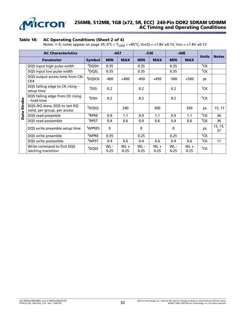
256MB, 512MB, 1GB (x72, SR, ECC) 240-Pin DDR2 SDRAM UDIMMAC Timing and Operating Conditions
Data
Str
ob
e
DQS input high pulse width tDQSH 0.35 0.35 0.35 tCKDQS input low pulse width tDQSL 0.35 0.35 0.35 tCKDQS output access time from CK/CK#
tDQSCK -400 +400 -450 +450 -500 +500 ps
DQS falling edge to CK rising – setup time
tDSS 0.2 0.2 0.2 tCK
DQS falling edge from CK rising – hold time
tDSH 0.2 0.2 0.2 tCK
DQS–DQ skew, DQS to last DQ valid, per group, per access
tDQSQ 240 300 350 ps 15, 17
DQS read preamble tRPRE 0.9 1.1 0.9 1.1 0.9 1.1 tCK 36DQS read postamble tRPST 0.4 0.6 0.4 0.6 0.4 0.6 tCK 36
DQS write preamble setup time tWPRES 0 0 0 ps12, 13,
37DQS write preamble tWPRE 0.35 0.25 0.25 tCKDQS write postamble tWPST 0.4 0.6 0.4 0.6 0.4 0.6 tCK 11Write command to first DQS latching transition
tDQSSWL - 0.25
WL + 0.25
WL - 0.25
WL + 0.25
WL - 0.25
WL + 0.25
tCK
Table 18: AC Operating Conditions (Sheet 2 of 4)Notes: 1–5; notes appear on page 35; 0°C ≤ TCASE ≤ +85°C; VDDQ = +1.8V ±0.1V, VDD = +1.8V ±0.1V
AC Characteristics -667 -53E -40EUnits Notes
Parameter Symbol MIN MAX MIN MAX MIN MAX
pdf: 09005aef80e6f860, source: 09005aef80e5b799 Micron Technology, Inc., reserves the right to change products or specifications without notice.HTF9C32_64_128x72AG_2.fm - Rev. C 6/05 EN 32 ©2003, 2004, 2005 Micron Technology, Inc. All rights reserved.
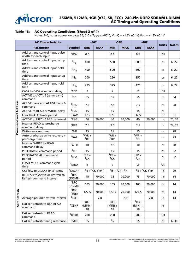
256MB, 512MB, 1GB (x72, SR, ECC) 240-Pin DDR2 SDRAM UDIMMAC Timing and Operating Conditions
Co
mm
an
d a
nd
Ad
dre
ss
Address and control input pulse width for each input
tIPW 0.6 0.6 0.6 tCK
Address and control input setup time
tISa 400 500 600 ps 6, 22
Address and control input hold time
tIHa 400 500 600 ps 6, 22
Address and control input setup time
tISb 200 250 350 ps 6, 22
Address and control input hold time
tIHb 275 375 475 ps 6, 22
CAS# to CAS# command delay tCCD 2 2 2 tCKACTIVE to ACTIVE (same bank) command
tRC 55 55 55 ns 34
ACTIVE bank a to ACTIVE bank b command
tRRD 7.5 7.5 7.5 ns 28
ACTIVE to READ or WRITE delay tRCD 15 15 15 nsFour Bank Activate period tFAW 37.5 37.5 37.5 ns 31ACTIVE to PRECHARGE command tRAS 40 70,000 40 70,000 40 70,000 ns 21, 34Internal READ to precharge command delay
tRTP 7.5 7.5 7.5 ns 24, 28
Write recovery time tWR 15 15 15 ns 28Auto precharge write recovery + precharge time
tDALtWR +
tRP
tWR + tRP
tWR + tRP
ns 23
Internal WRITE to READ command delay
tWTR 10 7.5 10 ns 28
PRECHARGE command period tRP 15 15 15 ns 32PRECHARGE ALL command period
tRPAtRP + tCK
tRP + tCK
tRP + tCK
ns 32
LOAD MODE command cycle time
tMRD 2 2 2 tCK
CKE low to CK,CK# uncertainty tDELAY tIS + tCK +tIH tIS + tCK +tIH tIS + tCK +tIH ns 29
Se
lf R
efr
esh
REFRESH to Active or Refresh to Refresh command interval
tRFC (256MB)
75 70,000 75 70,000 75 70,000 ns 14
tRFC (512MB)
105 70,000 105 70,000 105 70,000 ns 14
tRFC (1GB)
127.5 70,000 127.5 70,000 127.5 70,000 ns 14
Average periodic refresh interval tREFI 7.8 7.8 7.8 µs 14
Exit self refresh to non-READ command
tXSNR
tRFC(MIN) +
10
tRFC(MIN) +
10
tRFC(MIN) +
10ns
Exit self refresh to READ command
tXSRD 200 200 200 tCK
Exit self refresh timing reference tISXR tIS tIS tIS ps 6, 30
Table 18: AC Operating Conditions (Sheet 3 of 4)Notes: 1–5; notes appear on page 35; 0°C ≤ TCASE ≤ +85°C; VDDQ = +1.8V ±0.1V, VDD = +1.8V ±0.1V
AC Characteristics -667 -53E -40EUnits Notes
Parameter Symbol MIN MAX MIN MAX MIN MAX
pdf: 09005aef80e6f860, source: 09005aef80e5b799 Micron Technology, Inc., reserves the right to change products or specifications without notice.HTF9C32_64_128x72AG_2.fm - Rev. C 6/05 EN 33 ©2003, 2004, 2005 Micron Technology, Inc. All rights reserved.
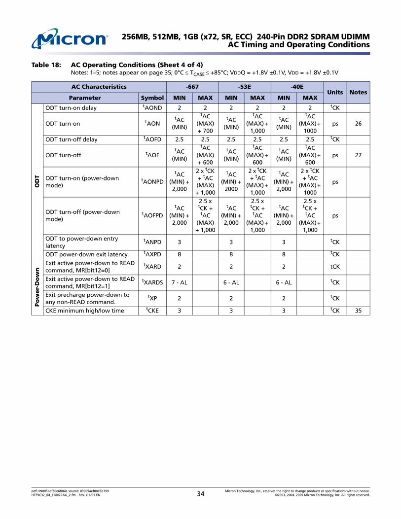
256MB, 512MB, 1GB (x72, SR, ECC) 240-Pin DDR2 SDRAM UDIMMAC Timing and Operating Conditions
OD
T
ODT turn-on delay tAOND 2 2 2 2 2 2 tCK
ODT turn-on tAONtAC
(MIN)
tAC (MAX) + 700
tAC(MIN)
tAC(MAX) +
1,000
tAC (MIN)
tAC (MAX) +
1000ps 26
ODT turn-off delay tAOFD 2.5 2.5 2.5 2.5 2.5 2.5 tCK
ODT turn-off tAOFtAC
(MIN)
tAC (MAX) + 600
tAC(MIN)
tAC(MAX) +
600
tAC (MIN)
tAC (MAX) +
600ps 27
ODT turn-on (power-down mode)
tAONPD
tAC(MIN) + 2,000
2 x tCK + tAC(MAX) + 1,000
tAC(MIN) +
2000
2 x tCK + tAC
(MAX) + 1,000
tAC(MIN) + 2,000
2 x tCK + tAC
(MAX) + 1000
ps
ODT turn-off (power-down mode)
tAOFPD
tAC (MIN) + 2,000
2.5 x
tCK + tAC
(MAX) + 1,000
tAC (MIN) + 2,000
2.5 x
tCK + tAC
(MAX) + 1,000
tAC (MIN) + 2,000
2.5 x
tCK + tAC
(MAX) + 1,000
ps
ODT to power-down entry latency
tANPD 3 3 3 tCK
ODT power-down exit latency tAXPD 8 8 8 tCK
Po
wer-
Do
wn
Exit active power-down to READ command, MR[bit12=0]
tXARD 2 2 2 tCK
Exit active power-down to READ command, MR[bit12=1]
tXARDS 7 - AL 6 - AL 6 - AL tCK
Exit precharge power-down to any non-READ command.
tXP 2 2 2 tCK
CKE minimum high/low time tCKE 3 3 3 tCK 35
Table 18: AC Operating Conditions (Sheet 4 of 4)Notes: 1–5; notes appear on page 35; 0°C ≤ TCASE ≤ +85°C; VDDQ = +1.8V ±0.1V, VDD = +1.8V ±0.1V
AC Characteristics -667 -53E -40EUnits Notes
Parameter Symbol MIN MAX MIN MAX MIN MAX
pdf: 09005aef80e6f860, source: 09005aef80e5b799 Micron Technology, Inc., reserves the right to change products or specifications without notice.HTF9C32_64_128x72AG_2.fm - Rev. C 6/05 EN 34 ©2003, 2004, 2005 Micron Technology, Inc. All rights reserved.
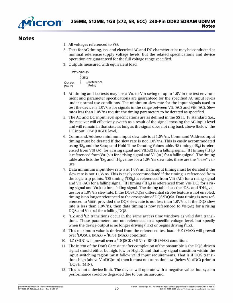
256MB, 512MB, 1GB (x72, SR, ECC) 240-Pin DDR2 SDRAM UDIMMNotes
Notes1. All voltages referenced to VSS.2. Tests for AC timing, IDD, and electrical AC and DC characteristics may be conducted at
nominal reference/supply voltage levels, but the related specifications and deviceoperation are guaranteed for the full voltage range specified.
3. Outputs measured with equivalent load:
4. AC timing and IDD tests may use a VIL-to-VIH swing of up to 1.0V in the test environ-ment and parameter specifications are guaranteed for the specified AC input levelsunder normal use conditions. The minimum slew rate for the input signals used totest the device is 1.0V/ns for signals in the range between VIL (AC) and VIH (AC). Slewrates less than 1.0V/ns require the timing parameters to be derated as specified.
5. The AC and DC input level specifications are as defined in the SSTL_18 standard (i.e.,the receiver will effectively switch as a result of the signal crossing the AC input leveland will remain in that state as long as the signal does not ring back above [below] theDC input LOW [HIGH] level).
6. Command/Address minimum input slew rate is at 1.0V/ns. Command/Address inputtiming must be derated if the slew rate is not 1.0V/ns. This is easily accommodatedusing tISb and the Setup and Hold Time Derating Values table. tIS timing (tISb) is refer-enced from VIH (AC) for a rising signal and VIL(AC) for a falling signal. tIH timing (tIHb)is referenced from VIH(AC) for a rising signal and VIL(DC) for a falling signal. The timingtable also lists the tISb and tIHb values for a 1.0V/ns slew rate; these are the “base” val-ues.
7. Data minimum input slew rate is at 1.0V/ns. Data input timing must be derated if theslew rate is not 1.0V/ns. This is easily accommodated if the timing is referenced fromthe logic trip points. tDS timing (tDSb) is referenced from VIH (AC) for a rising signaland VIL (AC) for a falling signal. tIH timing (tIHb) is referenced from VIH(DC) for a ris-ing signal and VIL(DC) for a falling signal. The timing table lists the tDSb and tDHb val-ues for a 1.0V/ns slew rate. If the DQS/DQS# differential strobe feature is not enabled,timing is no longer referenced to the crosspoint of DQS/DQS#. Data timing is now ref-erenced to VREF, provided the DQS slew rate is not less than 1.0V/ns. If the DQS slewrate is less than 1.0V/ns, then data timing is now referenced to VIH(AC) for a risingDQS and VIL(DC) for a falling DQS.
8. tHZ and tLZ transitions occur in the same access time windows as valid data transi-tions. These parameters are not referenced to a specific voltage level, but specifywhen the device output is no longer driving (tHZ) or begins driving (tLZ).
9. This maximum value is derived from the referenced test load. tHZ (MAX) will prevailover tDQSCK (MAX) + tRPST (MAX) condition.
10. tLZ (MIN) will prevail over a tDQSCK (MIN) + tRPRE (MAX) condition.11. The intent of the Don’t Care state after completion of the postamble is the DQS-driven
signal should either be high, low or High-Z and that any signal transition within theinput switching region must follow valid input requirements. That is if DQS transi-tions high (above VIHDC(min) then it must not transition low (below VIH(DC) prior totDQSH (MIN).
12. This is not a device limit. The device will operate with a negative value, but systemperformance could be degraded due to bus turnaround.
Output(VOUT)
Reference Point
25Ω
VTT = VDDQ/2
pdf: 09005aef80e6f860, source: 09005aef80e5b799 Micron Technology, Inc., reserves the right to change products or specifications without notice.HTF9C32_64_128x72AG_2.fm - Rev. C 6/05 EN 35 ©2003, 2004, 2005 Micron Technology, Inc. All rights reserved.
256MB, 512MB, 1GB (x72, SR, ECC) 240-Pin DDR2 SDRAM UDIMMNotes
13. It is recommended that DQS be valid (HIGH or LOW) on or before the WRITE com-mand. The case shown (DQS going from High-Z to logic LOW) applies when noWRITEs were previously in progress on the bus. If a previous WRITE was in progress,DQS could be HIGH during this time, depending on tDQSS.
14. The refresh period is 64ms. This equates to an average refresh rate of 7.8125µs. How-ever, a REFRESH command must be asserted at least once every 70.3µs or tRFC(MAX). To ensure all rows of all banks are properly refreshed, 8192 REFRESH com-mands must be issued every 64ms.
15. Each byte lane has a corresponding DQS.16. CK and CK# input slew rate must be ≥ 1V/ns (≥ 2 V/ns if measured differentially).17. The data valid window is derived by achieving other specifications - tHP. (tCK/2),
tDQSQ, and tQH (tQH = tHP - tQHS). The data valid window derates in direct propor-tion to the clock duty cycle and a practical data valid window can be derived.
18. tJIT specification is currently TBD.19. MIN(tCL, tCH) refers to the smaller of the actual clock low time and the actual clock
high time as provided to the device (i.e. This value can be greater than the minimumspecification limits for tCL and tCH). For example, tCL and tCH are = 50 percent of theperiod, less the half period jitter [tJIT(HP)] of the clock source, and less the half periodjitter due to cross talk [tJIT(cross talk)] into the clock traces.
20. tHP (MIN) is the lesser of tCL minimum and tCH minimum actually applied to thedevice CK and CK# inputs.
21. READs and WRITEs with auto precharge are allowed to be issued before tRAS (MIN) issatisfied since tRAS lockout feature is supported in DDR2 SDRAM devices.
22. VIL/VIH DDR2 overshoot/undershoot. REFER TO the 256Mb, 512Mb, or 1Gb DDR2SDRAM data sheet for more detail.
23. tDAL = (nWR) + (tRP/tCK): For each of the terms above, if not already an integer,round to the next highest integer. tCK refers to the application clock period; nWRrefers to the tWR parameter stored in the MR[11,10,9]. Example: For -53E at tCK = 3.75ns with tWR programmed to four clocks. tDAL = 4 + (15 ns/3.75 ns) clocks = 4 +(4)clocks = 8 clocks.
24. The minimum READ to internal PRECHARGE time. This parameter is only applicablewhen tRTP/(2*tCK) > 1. If tRTP/(2*tCK) ≤ 1, then equation AL + BL/2 applies. Notwith-standing, tRAS (MIN) has to be satisfied as well. The DDR2 SDRAM device will auto-matically delay the internal PRECHARGE command until tRAS (MIN) has beensatisfied.
25. Operating frequency is only allowed to change during self refresh mode, prechargepower-down mode, and system reset condition.
26. ODT turn-on time tAON (MIN) is when the device leaves high impedance and ODTresistance begins to turn on. ODT turn-on time tAON (MAX) is when the ODT resis-tance is fully on. Both are measured from tAOND.
27. ODT turn-off time tAOF (MIN) is when the device starts to turn off ODT resistance.ODT turn off time tAOF (MAX) is when the bus is in high impedance. Both are mea-sured from tAOFD.
28. This parameter has a two clock minimum requirement at any tCK.29. tDELAY is calculated from tIS + tCK + tIH so that CKE registration LOW is guaranteed
prior to CK, CK# being removed in a system RESET condition.30. tISXR is equal to tIS and is used for CKE setup time during self refresh exit.31. No more than 4 bank ACTIVE commands may be issued in a given tFAW(min) period.
tRRD(min) restriction still applies. The tFAW(min) parameter applies to all 8 bankDDR2 devices, regardless of the number of banks already open or closed.
pdf: 09005aef80e6f860, source: 09005aef80e5b799 Micron Technology, Inc., reserves the right to change products or specifications without notice.HTF9C32_64_128x72AG_2.fm - Rev. C 6/05 EN 36 ©2003, 2004, 2005 Micron Technology, Inc. All rights reserved.
256MB, 512MB, 1GB (x72, SR, ECC) 240-Pin DDR2 SDRAM UDIMMNotes
32. tRPA timing applies when the PRECHARGE(ALL) command is issued, regardless of thenumber of banks already open or closed. If a single-bank PRECHARGE command isissued, tRP timing applies. tRPA(MIN) applies to all 8-bank DDR2 devices.
33. Value is minimum pulse width, not the number of clock registrations.34. Applicable to Read cycles only. Write cycles generally require additional time due to
Write recovery time (tWR) during auto precharge.35. tCKE (MIN) of 3 clocks means CKE must be registered on three consecutive positive
clock edges. CKE must remain at the valid input level the entire time it takes toachieve the 3 clocks of registration. Thus, after any CKE transition, CKE may not tran-sition from its valid level during the time period of tIS + 2 x tCK + tIH.
36. This parameter is not referenced to a specific voltage level, but specified whwen thedevice output is no longer driving (tRPST) or beginning to drive (tRPRE).
37. When DQS is used single-ended, the minimum limit is reduced by 100ps.
pdf: 09005aef80e6f860, source: 09005aef80e5b799 Micron Technology, Inc., reserves the right to change products or specifications without notice.HTF9C32_64_128x72AG_2.fm - Rev. C 6/05 EN 37 ©2003, 2004, 2005 Micron Technology, Inc. All rights reserved.
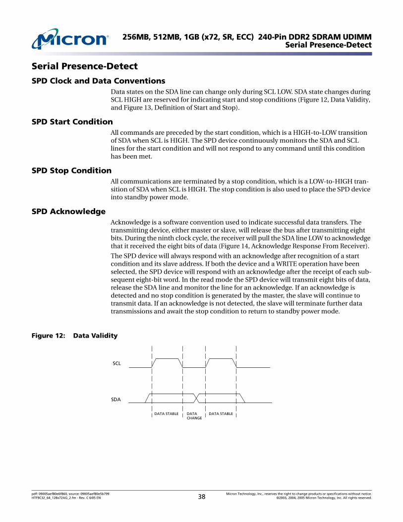
256MB, 512MB, 1GB (x72, SR, ECC) 240-Pin DDR2 SDRAM UDIMMSerial Presence-Detect
Serial Presence-Detect
SPD Clock and Data ConventionsData states on the SDA line can change only during SCL LOW. SDA state changes during SCL HIGH are reserved for indicating start and stop conditions (Figure 12, Data Validity, and Figure 13, Definition of Start and Stop).
SPD Start ConditionAll commands are preceded by the start condition, which is a HIGH-to-LOW transition of SDA when SCL is HIGH. The SPD device continuously monitors the SDA and SCL lines for the start condition and will not respond to any command until this condition has been met.
SPD Stop ConditionAll communications are terminated by a stop condition, which is a LOW-to-HIGH tran-sition of SDA when SCL is HIGH. The stop condition is also used to place the SPD device into standby power mode.
SPD AcknowledgeAcknowledge is a software convention used to indicate successful data transfers. The transmitting device, either master or slave, will release the bus after transmitting eight bits. During the ninth clock cycle, the receiver will pull the SDA line LOW to acknowledge that it received the eight bits of data (Figure 14, Acknowledge Response From Receiver).
The SPD device will always respond with an acknowledge after recognition of a start condition and its slave address. If both the device and a WRITE operation have been selected, the SPD device will respond with an acknowledge after the receipt of each sub-sequent eight-bit word. In the read mode the SPD device will transmit eight bits of data, release the SDA line and monitor the line for an acknowledge. If an acknowledge is detected and no stop condition is generated by the master, the slave will continue to transmit data. If an acknowledge is not detected, the slave will terminate further data transmissions and await the stop condition to return to standby power mode.
Figure 12: Data Validity
SCL
SDA
DATA STABLE DATA STABLEDATACHANGE
pdf: 09005aef80e6f860, source: 09005aef80e5b799 Micron Technology, Inc., reserves the right to change products or specifications without notice.HTF9C32_64_128x72AG_2.fm - Rev. C 6/05 EN 38 ©2003, 2004, 2005 Micron Technology, Inc. All rights reserved.
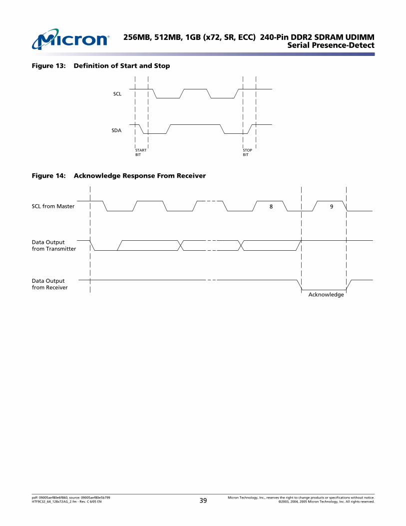
256MB, 512MB, 1GB (x72, SR, ECC) 240-Pin DDR2 SDRAM UDIMMSerial Presence-Detect
Figure 13: Definition of Start and Stop
Figure 14: Acknowledge Response From Receiver
SCL
SDA
STARTBIT
STOPBIT
SCL from Master
Data Outputfrom Transmitter
Data Outputfrom Receiver
98
Acknowledge
pdf: 09005aef80e6f860, source: 09005aef80e5b799 Micron Technology, Inc., reserves the right to change products or specifications without notice.HTF9C32_64_128x72AG_2.fm - Rev. C 6/05 EN 39 ©2003, 2004, 2005 Micron Technology, Inc. All rights reserved.
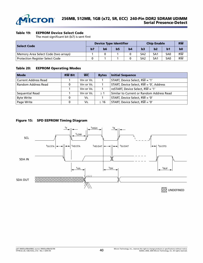
256MB, 512MB, 1GB (x72, SR, ECC) 240-Pin DDR2 SDRAM UDIMMSerial Presence-Detect
Figure 15: SPD EEPROM Timing Diagram
Table 19: EEPROM Device Select CodeThe most significant bit (b7) is sent first
Select CodeDevice Type Identifier Chip Enable RW
b7 b6 b5 b4 b3 b2 b1 b0
Memory Area Select Code (two arrays) 1 0 1 0 SA2 SA1 SA0 RW
Protection Register Select Code 0 1 1 0 SA2 SA1 SA0 RW
Table 20: EEPROM Operating Modes
Mode RW Bit WC Bytes Initial Sequence
Current Address Read 1 VIH or VIL 1 START, Device Select, RW = ‘1’Random Address Read 0 VIH or VIL 1 START, Device Select, RW = ‘0’, Address
1 VIH or VIL 1 reSTART, Device Select, RW = ‘1’Sequential Read 1 VIH or VIL ≥ 1 Similar to Current or Random Address ReadByte Write 0 VIL 1 START, Device Select, RW = ‘0’Page Write 0 VIL ≤ 16 START, Device Select, RW = ‘0’
SCL
SDA IN
SDA OUT
tLOW
tSU:STA tHD:STA
tF tHIGH tR
tBUFtDHtAA
tSU:STOtSU:DATtHD:DAT
UNDEFINED
pdf: 09005aef80e6f860, source: 09005aef80e5b799 Micron Technology, Inc., reserves the right to change products or specifications without notice.HTF9C32_64_128x72AG_2.fm - Rev. C 6/05 EN 40 ©2003, 2004, 2005 Micron Technology, Inc. All rights reserved.
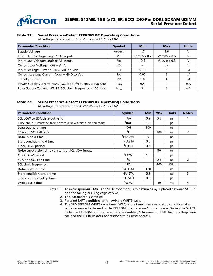
256MB, 512MB, 1GB (x72, SR, ECC) 240-Pin DDR2 SDRAM UDIMMSerial Presence-Detect
Notes: 1. To avoid spurious START and STOP conditions, a minimum delay is placed between SCL = 1 and the falling or rising edge of SDA.
2. This parameter is sampled.3. For a reSTART condition, or following a WRITE cycle.4. The SPD EEPROM WRITE cycle time (tWRC) is the time from a valid stop condition of a
write sequence to the end of the EEPROM internal erase/program cycle. During the WRITE cycle, the EEPROM bus interface circuit is disabled, SDA remains HIGH due to pull-up resis-tor, and the EEPROM does not respond to its slave address.
Table 21: Serial Presence-Detect EEPROM DC Operating ConditionsAll voltages referenced to VSS; VDDSPD = +1.7V to +3.6V
Parameter/Condition Symbol Min Max Units
Supply Voltage VDDSPD 1.7 3.6 V
Input High Voltage: Logic 1; All inputs VIH VDDSPD X 0.7 VDDSPD + 0.5 V
Input Low Voltage: Logic 0; All inputs VIL -0.6 VDDSPD x 0.3 V
Output Low Voltage: IOUT = 3mA VOL – 0.4 V
Input Leakage Current: VIN = GND to VDD ILI 0.10 3 µA
Output Leakage Current: VOUT = GND to VDD ILO 0.05 3 µA
Standby Current ISB 1.6 4 µA
Power Supply Current, READ: SCL clock frequency = 100 KHz ICCR 0.4 1 mA
Powr Supply Current, WRITE: SCL clock frequency = 100 KHz ICCW 2 3 mA
Table 22: Serial Presence-Detect EEPROM AC Operating ConditionsAll voltages referenced to VSS; VDDSPD = +1.7V to +3.6V
Parameter/Condition Symbol Min Max Units Notes
SCL LOW to SDA data-out valid tAA 0.2 0.9 µs 1
Time the bus must be free before a new transition can start tBUF 1.3 µs
Data-out hold time tDH 200 ns
SDA and SCL fall time tF 300 ns 2
Data-in hold time tHD:DAT 0 µs
Start condition hold time tHD:STA 0.6 µs
Clock HIGH period tHIGH 0.6 µs
Noise suppression time constant at SCL, SDA inputs tI 50 ns
Clock LOW period tLOW 1.3 µs
SDA and SCL rise time tR 0.3 µs 2
SCL clock frequency fSCL 400 KHz
Data-in setup time tSU:DAT 100 ns
Start condition setup time tSU:STA 0.6 µs 3
Stop condition setup time tSU:STO 0.6 µs
WRITE cycle time tWRC 10 ms 4
pdf: 09005aef80e6f860, source: 09005aef80e5b799 Micron Technology, Inc., reserves the right to change products or specifications without notice.HTF9C32_64_128x72AG_2.fm - Rev. C 6/05 EN 41 ©2003, 2004, 2005 Micron Technology, Inc. All rights reserved.
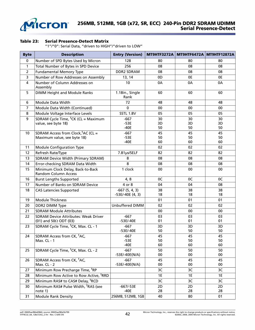
256MB, 512MB, 1GB (x72, SR, ECC) 240-Pin DDR2 SDRAM UDIMMSerial Presence-Detect
Table 23: Serial Presence-Detect Matrix“1”/“0”: Serial Data, “driven to HIGH”/“driven to LOW”
Byte Description Entry (Version) MT9HTF3272A MT9HTF6472A MT9HTF12872A
0 Number of SPD Bytes Used by Micron 128 80 80 801 Total Number of Bytes in SPD Device 256 08 08 082 Fundamental Memory Type DDR2 SDRAM 08 08 083 Number of Row Addresses on Assembly 13, 14 0D 0E 0E4 Number of Column Addresses on
Assembly10 0A 0A 0A
5 DIMM Height and Module Ranks 1.18in., Single Rank
60 60 60
6 Module Data Width 72 48 48 487 Module Data Width (Continued) 0 00 00 008 Module Voltage Interface Levels SSTL 1.8V 05 05 059 SDRAM Cycle Time, tCK (CL = Maximum
value, see byte 18)-667-53E-40E
303D50
303D50
303D50
10 SDRAM Access from Clock,tAC (CL = Maximum value, see byte 18)
-667-53E-40E
455060
455060
455060
11 Module Configuration Type 02 02 0212 Refresh Rate/Type 7.81µs/SELF 82 82 8213 SDRAM Device Width (Primary SDRAM) 8 08 08 0814 Error-checking SDRAM Data Width 8 08 08 0815 Minimum Clock Delay, Back-to-Back
Random Column Access1 clock 00 00 00
16 Burst Lengths Supported 4, 8 0C 0C 0C17 Number of Banks on SDRAM Device 4 or 8 04 04 0818 CAS Latencies Supported -667 (5, 4, 3)
-53E/-40E (4, 3)3818
3818
3818
19 Module Thickness 01 01 0120 DDR2 DIMM Type Unbuffered DIMM 02 02 0221 SDRAM Module Attributes 00 00 0022 SDRAM Device Attributes: Weak Driver
(01) and 50Ω ODT (03)-667
-53E/-40E0301
0301
0301
23 SDRAM Cycle Time, tCK, Max. CL - 1 -667-53E/-40E
3D50
3D50
3D50
24 SDRAM Access from CK, tAC, Max. CL - 1
-667-53E-40E
455060
455060
455060
25 SDRAM Cycle Time, tCK, Max. CL - 2 -667-53E/-40E(N/A)
5000
5000
5000
26 SDRAM Access from CK, tAC, Max. CL - 2
-667-53E/-40E(N/A)
4500
4500
4500
27 Minimum Row Precharge Time, tRP 3C 3C 3C28 Minimum Row Active to Row Active, tRRD 1E 1E 1E29 Minimum RAS# to CAS# Delay, tRCD 3C 3C 3C30 Minimum RAS# Pulse Width, tRAS (see
note 1)-667/-53E
-40E2D28
2D28
2D28
31 Module Rank Density 256MB, 512MB, 1GB 40 80 01
pdf: 09005aef80e6f860, source: 09005aef80e5b799 Micron Technology, Inc., reserves the right to change products or specifications without notice.HTF9C32_64_128x72AG_2.fm - Rev. C 6/05 EN 42 ©2003, 2004, 2005 Micron Technology, Inc. All rights reserved.
256MB, 512MB, 1GB (x72, SR, ECC) 240-Pin DDR2 SDRAM UDIMMSerial Presence-Detect
Notes: 1. The tRAS SPD value shown is based on the JEDEC standard value of 45 ns; the actual device specification is tRAS = 40ns.
32 Address and Command Setup Time, tISb -667-53E-40E
202535
202535
202535
33 Address and Command Hold Time, tIHb -667-53E-40E
273747
273747
273747
34 Data/ Data Mask Input Setup Time, tDSb -667/-53E-40E
1015
1015
1015
35 Data/ Data Mask Input Hold Time, tDHb -667-53E-40E
172227
172227
172227
36 Write Recovery Time, tWR 3C 3C 3C37 Write to Read CMD Delay, tWTR -667/-53E
-40E1E28
1E28
1E28
38 Read to Precharge CMD Delay, tRTP 1E 1E 1E39 Mem Analysis Probe 00 00 0040 Extension for bytes 41 and 42 00 00 0641 Min Active Auto Refresh Time, tRC -667/-53E
-40E3C37
3C37
3C37
42 Minimum Auto Refresh to Active/Auto Refresh Command Period, tRFC
4B 69 7F
43 SDRAM Device Max Cycle Time, tCKMAX 80 80 8044 SDRAM Device Max DQS-DQ Skew Time,
tDQSQ-667-53E-40E
181E23
181E23
181E23
45 SDRAM Device Max Read Data Hold Skew Factor, tQHS
-667-53E-40E
22282D
22282D
22282D
46 PLL Relock Time 00 00 0047–61 Optional features, not supported 00 00 00
62 SPD Revision Release 1.2 12 12 1263 Checksum For Bytes 0–62 -667
-53E-40E
FEA910
5D086F
FEA910
64 Manufacturer’s JEDEC ID Code MICRON 2C 2C 2C65-71 Manufacturer’s JEDEC ID Code (Continued) FF FF FF
72 Manufacturing Location 01–12 01–0C 01–0C 01–0C73-90 Module Part Number (ASCII) Variable Data Variable Data Variable Data
91 PCB Identification Code 1–9 01-09 01-09 01-0992 Identification Code (Continued) 0 00 00 0093 Year of Manufacture in BCD Variable Data Variable Data Variable Data94 Week of Manufacture in BCD Variable Data Variable Data Variable Data
95-98 Module Serial Number Variable Data Variable Data Variable Data99–127 Manufacturer-Specific Data (RSVD) – – –
Table 23: Serial Presence-Detect Matrix“1”/“0”: Serial Data, “driven to HIGH”/“driven to LOW”
Byte Description Entry (Version) MT9HTF3272A MT9HTF6472A MT9HTF12872A
pdf: 09005aef80e6f860, source: 09005aef80e5b799 Micron Technology, Inc., reserves the right to change products or specifications without notice.HTF9C32_64_128x72AG_2.fm - Rev. C 6/05 EN 43 ©2003, 2004, 2005 Micron Technology, Inc. All rights reserved.
256MB, 512MB, 1GB (x72, SR, ECC) 240-Pin DDR2 SDRAM UDIMMModule Dimensions
Module DimensionsAll dimensions are in inches (millimeters); or typical where noted.
The dimensional diagram is for reference only. Refer to the MO document for complete design dimensions.
Figure 16: 240-pin DIMM DDR2 Module Dimensions
Data Sheet DesignationReleased (No Mark): This data sheet contains minimum and maximum limits specified over the complete power supply and temperature range for production devices. Although considered final, these specifications are subject to change, as further product development and data characterization sometimes occur.
MAXMIN
1.200 (30.50)1.175 (29.85)
PIN 1
0.700 (17.78)TYP.
0.098 (2.50) D(2X)
0.091 (2.30) TYP.
0.197 (5.0) TYP.
4.840 (123.0)TYP.
0.039 (1.0)TYP.
0.031 (0.80)TYP.
0.079 (2.00) R(4X)
0.030 (0.76) R
PIN 120
FRONT VIEW5.256 (133.50)5.244 (133.20)
2.165 (55.0)TYP.
2.48 (63.0)TYP.
0.394 (10.00)TYP.
BACK VIEW
PIN 240 PIN 121
0.054 (1.37)0.046 (1.17)
0.106 (2.70)MAX
U1 U2 U3 U4
U10
U6 U7 U8 U9
No Components This Side of Module
U5
®
8000 S. Federal Way, P.O. Box 6, Boise, ID 83707-0006, Tel: [email protected] www.micron.com Customer Comment Line: 800-932-4992
Micron, the M logo, and the Micron logo are trademarks of Micron Technology, Inc. All other trademarks are the property of their respective owners.
This data sheet contains minimum and maximum limits specified over the complete power supply and temperature range for production devices. Although considered final, these specifications are subject to change, as further product
development and data characterization sometimes occur.
pdf: 09005aef80e6f860, source: 09005aef80e5b799 Micron Technology, Inc., reserves the right to change products or specifications without notice.HTF9C32_64_128x72AG_2.fm - Rev. C 6/05 EN 44 ©2003, 2004, 2005 Micron Technology, Inc. All rights reserved.