Embed Size (px)
Citation preview

866 IEEE TRANSACTIONS ON MICROWAVE THEORY AND TECHNIQUES, VOL. 59, NO. 4, APRIL 2011
A 1.2–1.6-GHz Substrate-Integrated-WaveguideRF MEMS Tunable Filter
Vikram Sekar, Student Member, IEEE, Marcelino Armendariz, Member, IEEE, and Kamran Entesari, Member, IEEE
Abstract—This paper presents a high-performance substrate-in-tegrated-waveguide RF microelectromechanical systems (MEMS)tunable filter for 1.2–1.6-GHz frequency range. The proposedfilter is developed using packaged RF MEMS switches and utilizesa two-layer structure that effectively isolates the cavity filter fromthe RF MEMS switch circuitry. The two-pole filter implementedon RT/Duroid 6010LM exhibits an insertion loss of 2.2–4.1 dB anda return loss better than 15 dB for all tuning states. The relativebandwidth of the filter is 3.7 0.5% over the tuning range. Themeasured of the filter is 93–132 over the tuning range, whichis the best reported in filters using off-the-shelf RF MEMSswitches on conventional printed circuit board substrates. In ad-dition, an upper stopband rejection better than 28 dB is obtainedup to 4.0 GHz by employing low-pass filters at the bandpass filterterminals at the cost of 0.7–1.0-dB increase in the insertion loss.
Index Terms—RF microelectromechanical systems (RF MEMS),spurious suppression, substrate integrated waveguide (SIW), tun-able filter.
I. INTRODUCTION
L OW-LOSS tunable filters are essential componentsin multiband communication systems and wideband
tracking receivers. Recently, tunable filters at frequencies10 GHz employing RF microelectromechanical systems (RF
MEMS) switches have demonstrated high quality factor ,wide tuning range and high linearity, while having zero powerconsumption [1]. Since RF MEMS switches are inherentlyvery low loss, the of planar tunable filters, and consequently,insertion loss, is mostly limited by the resonator .
In recent years, a wide variety of planar techniques resultingin filter values between 50–170 have been reported [2]–[4].These filters require the RF MEMS switches to be constructedmonolithically along with the filter structure for good perfor-mance. To drastically improve the filter , an RF MEMS tun-able filter from 4–6 GHz using evanescent-mode waveguidecavities was developed in [5] and resulted in exceptionalvalues from 300 to 500 over the tuning range. Here, the valueis only limited by the losses in the RF MEMS switches since
Manuscript received August 05, 2010; revised December 13, 2010; acceptedDecember 22, 2010. Date of publication February 24, 2011; date of current ver-sion April 08, 2011. This work was supported by the National Science Founda-tion (NSF) under Grant 0901088.
V. Sekar and K. Entesari are with the Department of Electrical and ComputerEngineering, Texas A&M University, College Station, TX 77843 USA (e-mail:[email protected]; [email protected]).
M. Armendariz is with Raytheon, Dallas, TX 75243 USA (e-mail: [email protected]).
Color versions of one or more of the figures in this paper are available onlineat http://ieeexplore.ieee.org.
Digital Object Identifier 10.1109/TMTT.2011.2109006
waveguide cavity resonators have very high ( 1000). Thisfilter requires a fabricated monolithic MEMS chip module in-serted into the waveguide structure to implement the tunablefilter. As a result, the fabrication of filters reported in [2]–[5]is complicated and requires expensive microfabrication tech-nology.
Recently, there has also been a drive toward using commer-cially available surface-mount RF MEMS switches for the de-velopment of tunable filters using conventional printed circuitboard (PCB) etching technology. A 4-bit lumped-element tun-able filter from 25 to 75 MHz was demonstrated in [6] using RFMEMS switches developed by Radant MEMS Inc.1 An accu-rate model of the RF MEMS switch including package parasiticswas developed for successful filter design. The reported valuewas between 50–70 due to limited of the surface mount induc-tors. Using the same packaged switch, a planar switched filterwith around 75 was developed in the 1.5–2.3-GHz frequencyrange [7]. However, factors 100 are difficult to achieveusing packaged RF MEMS switches and planar filter topolo-gies due to limited of planar and surface-mount componentsat microwave frequencies.
As an alternative to planar filters, substrate-integrated-wave-guide (SIW) filters on planar dielectric substrates have been pro-posed due to their high quality factor [8], [9]. Such filters pro-vide a low-profile low-cost alternative to bulky metallic wave-guide filters and are fabricated using conventional PCB tech-nology. In [10], a method has been proposed to tune the reso-nant frequency of a SIW cavity resonator by 5% around 10 GHzbased on vertical tuning posts within the cavity and metal stripsthat emulate the presence of a closed switch. This technique isextended to a tunable filter with six tuning states from 1.5 to2.0 GHz developed by the authors using p-i-n diodes with afactor between 100–120 [11]. However, utilizing p-i-n diodesfor filter tuning results in intermodulation distortion and powerconsumption. Recently, RF MEMS switch technology has beenemployed to develop a tunable SIW filter on a low-temperatureco-fired ceramic (LTCC) substrate with limited tuning range( 7%) [12].
In this paper, a SIW RF MEMS tunable filter with 28% tuningrange from 1.2 to 1.6 GHz and quality factor between 93–132is presented for the first time. The frequency band is coveredby 14 tuning responses (states) with very fine frequency resolu-tion so as to behave as a continuous-type filter. Vertical tuningposts are used for frequency tuning by employing packaged RFMEMS switches from the Omron Corporation2 because theycan be directly soldered on to the filter circuit without utilizing
1Radant MEMS Inc., Stow, MA. [Online]. Available: www.radantmems.com.2Omron Corporation, Kyoto, Japan. [Online]. Available: www.omron.com.
0018-9480/$26.00 © 2011 IEEE

SEKAR et al.: 1.2–1.6-GHz SIW RF MEMS TUNABLE FILTER 867
wirebonds. As a result, the package parasitics are reduced con-siderably enabling the realization of a high-performance tun-able filter. The tunable filter is constructed using a two-layerstructure to isolate the RF MEMS switches and biasing linesfrom the SIW filter. Using low-pass filters (LPFs) at the filterinput/output, the upper stopband performance of the tunablebandpass filter is greatly improved.
II. TUNABLE RESONATOR STRUCTURE
A. SIW Cavity
Fig. 1(a) and (b) shows the top and cross-sectional views ofthe two-layer SIW cavity resonator that is tuned using pack-aged RF MEMS switches, respectively. The bottom substrateof height is used to design the SIW cavity with widthand length , where the top and bottom cavity walls are formedby the middle and bottom metal layers, respectively. The res-onator sidewalls are formed by periodic vias of diameter with acenter-to-center pitch between adjacent via holes. A thick sub-strate is utilized for the SIW cavity to minimize the conductorlosses in the waveguide [13]. To access the cavity and perform
-parameter measurement using SMA connectors, microstripfeed lines need to be on the top metal layer. They are con-nected to the tapered microstrip lines on the middle metal layerusing via-holes. The additional insertion loss of the via-holesthrough the thin top substrate layer with height is negli-gible ( 0.01 dB) in the 1–2-GHz frequency range. The taperedmicrostrip lines excite the cavity by gradually converting thequasi-TEM waves in the microstrip lines into -mode wavesinside the SIW sections of length . The amount of energycoupled into the cavity depends on the width of the inductiveirises, , at the input/output of the cavity. In addition, using atop substrate layer of height allows placement of tuning el-ements and associated bias-line routing (not shown) on the topmetal layer without affecting the SIW cavity performance.
To design the filter passband, the dominant -mode res-onance at a frequency is employed, and is given by
(1)
where is the velocity of light in vacuum and and are therelative permeability and permittivity of the substrate, respec-tively [9]. A higher order resonance mode is also excitedin a waveguide cavity and leads to poor upper stopband per-formance when used in filter design. However, by orienting thecavity excitations along adjacent sidewalls, the SIW cavity actsas a dual-mode resonator that provides a transmission zero in theupper passband due to cancellation of signals passing throughthe and modes, thereby improving stopband re-jection performance [9]. The position of the transmission zerodepends on the relative coupling of the incident wave to the
and modes, and can be controlled by adjustingthe relative distance between input and output excitations [14].
Fig. 1. (a) Top view of the tunable SIW cavity using packaged RF MEMSswitches. (b)�–� cross section of the tuning cavity. (c) Top view of the tuningelement employing an RF MEMS switch package, two tuning posts and a topvia. (d) �–� cross section of the tuning element.
B. Tuning Mechanism
To make the resonator tunable, tuning elements consistingof via-posts and RF MEMS switches are placed at variouslocations within the cavity, as shown in Fig. 1(a). The topand cross-sectional views of a tuning element are shown inFig. 1(c) and (d), respectively. Metallic vias between the topand bottom metal layers are used to change the cavity resonancefrequency, and are hence called tuning posts. To avoid shortinga tuning post to the cavity top wall (middle metal layer), squareopenings with edge in the cavity top wall are placed aroundeach tuning post. Since these openings are small compared tothe dimensions of the cavity, the cavity fields remain relativelyunaffected.
To change the dominant cavity resonance frequency, tuningposts in the cavity are connected to the cavity top wall (middlemetal layer) through top vias located between the top and middle

868 IEEE TRANSACTIONS ON MICROWAVE THEORY AND TECHNIQUES, VOL. 59, NO. 4, APRIL 2011
Fig. 2. (a) Photograph and structure of the packaged SPDT RF MEMS switch.(b) Side view of the SPST switch. (c) Schematic of the SPDT switch. (d) Mea-sured �-parameters of the RF MEMS switch.
metal layers, by closing RF MEMS switches appropriately. Byeffectively shorting the tuning posts to the cavity top wall, theresulting cavity field perturbation causes a shift in resonancefrequency. However, when all RF MEMS switches are open,each tuning post is isolated from the cavity top wall. Hence, thedominant fields inside the cavity remain relatively un-perturbed and the resulting resonance frequency is very closeto . The tuning range is maximized by reducing the para-sitic elements between the tuning post and cavity top wall. Thisimplies that the upper substrate layer must be thin so that the in-ductance of the top via is small. The parasitics associated withthe packaged RF MEMS switches and mounting pads also im-pose tuning limitations. For maximum tuning, every tuning post
TABLE ICAVITY PARAMETERS
Fig. 3. Surface current distribution on the tuning post and vector magnetic fielddistribution within the cavity resonator at resonance frequency, when tuning postP is: (a) disconnected and (b) connected.
and top via must be located as close as possible to the mountingpad of an RF MEMS switch package. Otherwise, the increasedinductance from the metal line connecting the tuning post (ortop via) to the switch mounting pad decreases the amount offrequency shift, and limits the filter tuning range. Hence, thelocations of tuning posts and top via are fixed with respect toa single RF MEMS switch package, and depend on the place-ment of mounting pads in the layout footprint of the switchpackage. This practical consideration imposes a design con-straint on the allowable locations for a pair of tuning posts. Asa result, extra tuning posts may be required to achieve symmet-rical tuning states, as discussed in Section III-C. The details ofthe RF MEMS switch package are provided in Section II-C.
C. Packaged RF MEMS Switch
The RF MEMS switch package (2SMES-01) from the OmronCorporation is shown in Fig. 2(a) and consists of a single-poledual-throw (SPDT) RF MEMS switch in which each switch canbe controlled individually. The SPDT switch has been testedto 100 million cycles for 32 units by the Omron Corpora-tion [15]. The cross-sectional view of one switch is shown inFig. 2(b). Each RF MEMS switch is a fixed-fixed bridge struc-ture constructed on glass substrate using movable silicon elec-trodes and gold metal contacts [16]. When a dc voltage is ap-plied, the switch connects the Cr/Au coplanar waveguide (CPW)signal lines present at the RF ports of the RF MEMS switchpackage and disconnects them when the biasing voltage is re-moved. Two such RF MEMS switches are flip-chip mounted ona ceramic package and nitrogen sealed in a hollow glass capusing frit-glass sealing. A resin is then applied on top to protect
SEKAR et al.: 1.2–1.6-GHz SIW RF MEMS TUNABLE FILTER 869
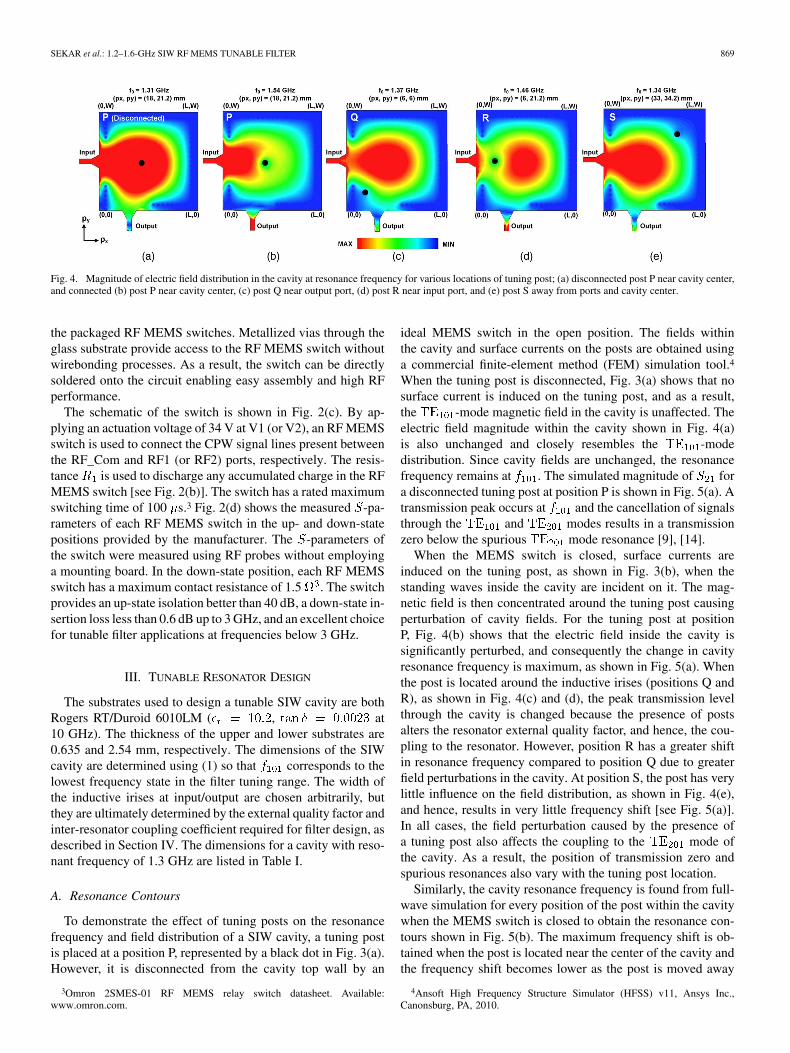
Fig. 4. Magnitude of electric field distribution in the cavity at resonance frequency for various locations of tuning post; (a) disconnected post P near cavity center,and connected (b) post P near cavity center, (c) post Q near output port, (d) post R near input port, and (e) post S away from ports and cavity center.
the packaged RF MEMS switches. Metallized vias through theglass substrate provide access to the RF MEMS switch withoutwirebonding processes. As a result, the switch can be directlysoldered onto the circuit enabling easy assembly and high RFperformance.
The schematic of the switch is shown in Fig. 2(c). By ap-plying an actuation voltage of 34 V at V1 (or V2), an RF MEMSswitch is used to connect the CPW signal lines present betweenthe RF_Com and RF1 (or RF2) ports, respectively. The resis-tance is used to discharge any accumulated charge in the RFMEMS switch [see Fig. 2(b)]. The switch has a rated maximumswitching time of 100 s.3 Fig. 2(d) shows the measured -pa-rameters of each RF MEMS switch in the up- and down-statepositions provided by the manufacturer. The -parameters ofthe switch were measured using RF probes without employinga mounting board. In the down-state position, each RF MEMSswitch has a maximum contact resistance of 1.5 . The switchprovides an up-state isolation better than 40 dB, a down-state in-sertion loss less than 0.6 dB up to 3 GHz, and an excellent choicefor tunable filter applications at frequencies below 3 GHz.
III. TUNABLE RESONATOR DESIGN
The substrates used to design a tunable SIW cavity are bothRogers RT/Duroid 6010LM ( , at10 GHz). The thickness of the upper and lower substrates are0.635 and 2.54 mm, respectively. The dimensions of the SIWcavity are determined using (1) so that corresponds to thelowest frequency state in the filter tuning range. The width ofthe inductive irises at input/output are chosen arbitrarily, butthey are ultimately determined by the external quality factor andinter-resonator coupling coefficient required for filter design, asdescribed in Section IV. The dimensions for a cavity with reso-nant frequency of 1.3 GHz are listed in Table I.
A. Resonance Contours
To demonstrate the effect of tuning posts on the resonancefrequency and field distribution of a SIW cavity, a tuning postis placed at a position P, represented by a black dot in Fig. 3(a).However, it is disconnected from the cavity top wall by an
3Omron 2SMES-01 RF MEMS relay switch datasheet. Available:www.omron.com.
ideal MEMS switch in the open position. The fields withinthe cavity and surface currents on the posts are obtained usinga commercial finite-element method (FEM) simulation tool.4
When the tuning post is disconnected, Fig. 3(a) shows that nosurface current is induced on the tuning post, and as a result,the -mode magnetic field in the cavity is unaffected. Theelectric field magnitude within the cavity shown in Fig. 4(a)is also unchanged and closely resembles the -modedistribution. Since cavity fields are unchanged, the resonancefrequency remains at . The simulated magnitude of fora disconnected tuning post at position P is shown in Fig. 5(a). Atransmission peak occurs at and the cancellation of signalsthrough the and modes results in a transmissionzero below the spurious mode resonance [9], [14].
When the MEMS switch is closed, surface currents areinduced on the tuning post, as shown in Fig. 3(b), when thestanding waves inside the cavity are incident on it. The mag-netic field is then concentrated around the tuning post causingperturbation of cavity fields. For the tuning post at positionP, Fig. 4(b) shows that the electric field inside the cavity issignificantly perturbed, and consequently the change in cavityresonance frequency is maximum, as shown in Fig. 5(a). Whenthe post is located around the inductive irises (positions Q andR), as shown in Fig. 4(c) and (d), the peak transmission levelthrough the cavity is changed because the presence of postsalters the resonator external quality factor, and hence, the cou-pling to the resonator. However, position R has a greater shiftin resonance frequency compared to position Q due to greaterfield perturbations in the cavity. At position S, the post has verylittle influence on the field distribution, as shown in Fig. 4(e),and hence, results in very little frequency shift [see Fig. 5(a)].In all cases, the field perturbation caused by the presence ofa tuning post also affects the coupling to the mode ofthe cavity. As a result, the position of transmission zero andspurious resonances also vary with the tuning post location.
Similarly, the cavity resonance frequency is found from full-wave simulation for every position of the post within the cavitywhen the MEMS switch is closed to obtain the resonance con-tours shown in Fig. 5(b). The maximum frequency shift is ob-tained when the post is located near the center of the cavity andthe frequency shift becomes lower as the post is moved away
4Ansoft High Frequency Structure Simulator (HFSS) v11, Ansys Inc.,Canonsburg, PA, 2010.

870 IEEE TRANSACTIONS ON MICROWAVE THEORY AND TECHNIQUES, VOL. 59, NO. 4, APRIL 2011
Fig. 5. (a) Simulated magnitude of � for the tuning post configurations inFig. 4. (b) Resonance contours for a single tuning post within the cavity.
from the center. Interestingly, the resonance contours closely re-semble the electric and magnetic field distributions of themode within the cavity [see Figs. 3(a), 4(a)]. Placing the metallicpost at points of maximum electric field or minimum magneticfield magnitudes produces large frequency shift.
To qualitatively understand this effect, the SIW cavity can beassumed to be a parallel L–C resonator with a resonance fre-quency . Since surface currents are induced onthe tuning post when it is connected inside a cavity (Fig. 3), thetuning post can equivalently be represented by a shunt induc-tance [17]. The value of the shunt inductance depends onthe electric field magnitudes at the position of the post and canbe calculated for a cavity using formulas in [17]. Aroundthe center of the cavity, where the electric field magnitudes arehighest, the value of is minimum. Thus, for a tuning postaround the center of the cavity, the resonance frequency shiftsto its highest value, which is given by , where
is the parallel combination of and . By properly con-trolling the position of the tuning post, the resonant frequency ofthe cavity can be adjusted to a desired value. The dependence offrequency shift on the field magnitudes within the cavity formsthe basis for design of the tunable SIW resonator.
B. External Quality Factor
While the contours in Fig. 5(b) imply that there are multiplepost positions for a given resonant frequency, some of these po-
Fig. 6. Normalized variation of external quality factor for various locations ofthe tuning post with respect to: (a) input port and (b) output port.
Fig. 7. (a) Tunable SIW resonator employing six tuning posts controlled bythree SPDT RF MEMS switch packages. (b) Coarse tuning states obtained usingonly tuning posts ����.
sitions affect the coupling to the cavity. In a tunable filter, devi-ation of coupling coefficients from the designed value results inbandwidth variation and matching degradation. To find these po-sitions, external quality factor at the input and output portsis evaluated using full-wave simulations for a singly loaded res-onator, as the position of the post is varied. The width of the in-ductive irises, , is assumed unchanged. The variation ofis normalized to the external quality factor of the cavity with nopost present, to obtain a normalized value, .
The variation of with post position at input and outputports is shown in Fig. 6(a) and (b). At both input and outputports, the external quality factor drastically increases if the postis located close to the input/output inductive irises because thepost affects coupling to the cavity. Thus, tuning posts must beplaced sufficiently far away from the inductive irises to avoid

SEKAR et al.: 1.2–1.6-GHz SIW RF MEMS TUNABLE FILTER 871
TABLE IIPOSITIONS OF TUNING POSTS
matching and bandwidth degradation as the filter is tuned. Iflarge frequency shifts are desired, tuning posts must be locatedaround the middle of the cavity where shows relatively lessvariation. Placing tuning posts away from the center, and towardthe top or right walls of the cavity provides smaller frequencyshifts while maintaining relatively constant .
C. Tunable Cavity Implementation
To implement a tunable cavity resonator with maximumtuning range and 16 symmetric tuning states, six tuning posts
controlled by three RF MEMS switch packagesare used, as shown in Fig. 7(a). Four tuning postslocated around the middle of the cavity are used
for coarse tuning control of the resonator because they producehigh-frequency shifts. Two tuning posts located awayfrom the middle and toward the top of the cavity provide smallfrequency shifts and are used for fine tuning control. Althoughthe fine tuning posts may also be placed near the right wallof the cavity, the proposed locations allow easy routing ofbias lines to the switch package. The positions of tuning postsare always such that the coupling mechanism to the cavity isrelatively unaffected. Accordingly, the regions in Fig. 6 corre-sponding to high values of are avoided. Also, the tuningposts and top via corresponding to a MEMS switch package areplaced as close as possible to the mounting pads of the packageto minimize parasitic elements and extend the tuning range.
The positions of the coarse tuning posts are optimized byfull-wave simulation in Sonnet5 using -parameters of the RFMEMS switch in Fig. 2(d) so that maximum frequency shift isobtained when all switches are in the closed position. Althoughit seems that four tuning posts are sufficient to give dis-tinct tuning frequencies, it is difficult to obtain maximum tuningrange with symmetric tuning frequencies simultaneously. Theoptimized positions of the coarse tuning posts shown in Table IIfor the cavity with dimensions given in Table I provide around30% tuning range. The 16 possible coarse tuning states areshown in Fig. 7(b) where state 1 corresponds to(all switches in the open position), and state 16 correspondsto (all switches in the closed position). Thetuning frequencies obtained with only coarse tuning posts arenonmonotonic and have unequal spacings between each other,and some of the states are unacceptable for a tunable filter withsymmetrically located tuning states. However, coarse tuningstates that are equally spaced and monotonically increasing, asshown in the inset of Fig. 7(b), can be used to obtain symmetrictuning capability with the help of fine tuning posts.
The fine tuning posts are designed to obtain linearlyincreasing fine tuning states between two coarse tuning states.
5Sonnet 12.52, Sonnet Software Inc., Syracuse, NY, 2009.
TABLE IIICOARSE AND FINE TUNING CONFIGURATIONS
Fig. 8. Simulated resonant frequency of the SIW cavity for different tuningstates.
The fine tuning post locations obtained from full-wave simula-tions are given in Table II. For each coarse tuning configuration
, three fine tuning states may be obtained using postsand . The allowable post configurations for coarse and fine
tuning are shown in Table III. The fine tuning stateis not utilized because the frequency increment produced is al-most the same as that of . This is because the elec-tric field magnitude at the location of post is low due to thefield perturbation caused by the connected post . As a result,the frequency increments for fine tuning states and
have similar values due to negligible field pertur-bation caused by post , when post is connected to the topcavity wall.
The proposed coarse and fine tuning mechanism results in 15frequency states, as shown in Fig. 8. The coarse and fine tuningconfigurations corresponding to each state are represented bya tuning code where is the coarse tuningconfiguration and is the fine tuning configuration.However, states 9 and 10 with configurations and havethe same resonance frequency. Thus, only state 9 is used, re-sulting in 14 distinct cavity tuning states.
Fig. 9 shows the simulated resonator unloaded quality factorfor 14 different tuning states. This is done using full-
wave simulation of a single resonator weakly coupled at theinput and output ports by employing the switch -parameters inFig. 2(d). The resonator has highest when all switches arein the up-state position (state 1), but decreases when a singleMEMS switch is closed due to the down-state resistance of the

872 IEEE TRANSACTIONS ON MICROWAVE THEORY AND TECHNIQUES, VOL. 59, NO. 4, APRIL 2011
Fig. 9. Simulated unloaded quality factor �� � of the SIW cavity for differenttuning states.
Fig. 10. Layout of the two-pole SIW RF MEMS tunable filter.
RF MEMS switch. For states 2–4, it is also seen that de-creases as a single tuning post approaches regions with higherelectric field magnitude near the center of the cavity. For states5–6, two tuning posts are connected and further decreasesdue to extra losses in fine tuning posts. For tuning states 7–14,two or more connected tuning posts result in high cavity fieldperturbation. As a result, values no longer follow a simpletrend, and vary between 93–108. The lowest correspondsto state 14 due to down-state resistances of five RF MEMSswitches in configuration .
IV. FILTER DESIGN
Since the upper transmission zero generated due to cancella-tion of the and modes is sufficiently far away fromthe filter passband, a pure Chebyshev response in the filter pass-band can be achieved. Fig. 10 shows the layout of the two-pole3.5% tunable SIW filter. The inter-resonator coupling coeffi-cient and the external quality factor are calculated usinglow-pass Chebyshev prototype values as [18]
(2)
where denotes the filter fractional bandwidth. For0.01-dB passband ripple, these formulas result inand , respectively.
To determine the coupling coefficient , the input/outputports are weakly coupled to the cavities with all MEMS switchesin the open position, using narrow inductive irises at the input/output. The width of the inductive iris between resonators, ,
is then adjusted to obtain the required coupling value, which isgiven by [18]
(3)
where and are the odd- and even-mode resonance frequen-cies, respectively, obtained from full-wave simulations when thetwo resonators are weakly coupled to the input/output ports.Next, the width of the input/output inductive iris, , is ad-justed to obtain the required value of . This can be extractedfrom full-wave simulation of a singly loaded cavity resonatorwith all MEMS switches in the open position, by employing theexpression [18]
(4)
where is the resonant frequency of the cavity andare the frequencies corresponding to a phase shift of 90 inthe simulated of the cavity, respectively. The final widthsof inductive irises used for filter design are mm and
mm, respectively.The entire tunable filter is simulated using Sonnet to take into
account all parasitics associated with mounting pads on the toplayer and bias line routing to the RF MEMS switches. The -pa-rameters of each RF MEMS switch are included in the completefilter simulation and the whole filter is fine tuned to achieve sym-metric tuning states with maximum return loss. The simulatedinsertion loss and return loss for the tunable SIW filter are shownin Fig. 11(a) and (b).
V. FABRICATION AND MEASUREMENT
A. Fabrication, Implementation, and Biasing
The photograph of the 1.2–1.6-GHz SIW RF MEMS tunablefilter fabricated on a two-layer RT/Duroid 6010LM substratewhose parameters are given in Section III is shown in Fig. 12.First, the mounting pads and bias lines for the RF MEMSswitches, and 50- feed lines to the filter are etched on thetop-side metallization of the upper substrate. The middle layer,which has tapered microstrip transitions and the cavity top wallwith openings for tuning posts (Fig. 1), is then etched on thebackside of the 0.635-mm-thick substrate. The top vias con-necting the top metal layer to the cavity top wall on the middlelayer are fabricated on the upper substrate using metallizedplated via-holes with 0.6-mm diameter.
Next, the topside metallization of the 2.54-mm-thick sub-strate is completely removed, while the backside metallizationis preserved to form the cavity bottom wall. The backside of theupper substrate is bonded to the topside of the lower substrateusing standard glass fiber (GF) pre-preg materialwith a thickness of 0.09 mm. Full-wave simulation of the filtershows that the GF pre-preg bonding material does not affectthe performance of the cavity filter. Then, plated via-holes with0.6-mm diameter are drilled through both substrates at appro-priate locations to form the tuning posts and sidewalls of theSIW filter. Packaged RF MEMS switches (2SMES-01) from theOmron Corporation are soldered onto the mounting pads on thetop layer. A 1-M resistor is connected between each bias

SEKAR et al.: 1.2–1.6-GHz SIW RF MEMS TUNABLE FILTER 873
Fig. 11. Simulated: (a) insertion loss and (b) return loss of the two-pole1.2–1.6-GHz tunable SIW filter.
Fig. 12. Fabricated 1.2–1.6-GHz SIW RF MEMS tunable filter.
line and dc ground to provide a discharge path for accumulatedcharge in each MEMS switch. DC ground is easily accessedthrough a via connecting the top-layer to the cavity top wall lo-cated in the middle layer. Since this dc ground via lies above theSIW cavity, it does not interfere with the RF performance of thecavity.
B. Measurements
The fabricated filter is measured using an Agilent N5230Avector network analyzer after calibration with the short-open-load-thru (SOLT) technique. The calibration is performed to the
Fig. 13. Measured: (a) insertion loss and (b) return loss of the two-pole1.2–1.6-GHz tunable SIW filter.
SMA connectors at the input/output of the filter, as indicated bythe reference planes and in Fig. 12. The measured insertionand return losses of the tunable SIW filter for 14 different statesare shown in Fig. 13(a) and (b), respectively. The measured in-sertion loss response includes the losses of the SMA connectorsat the filter input/output, which is negligible ( 0.1 dB) at around1–2 GHz. The measured return loss is better than 15 dB for alltuning states.
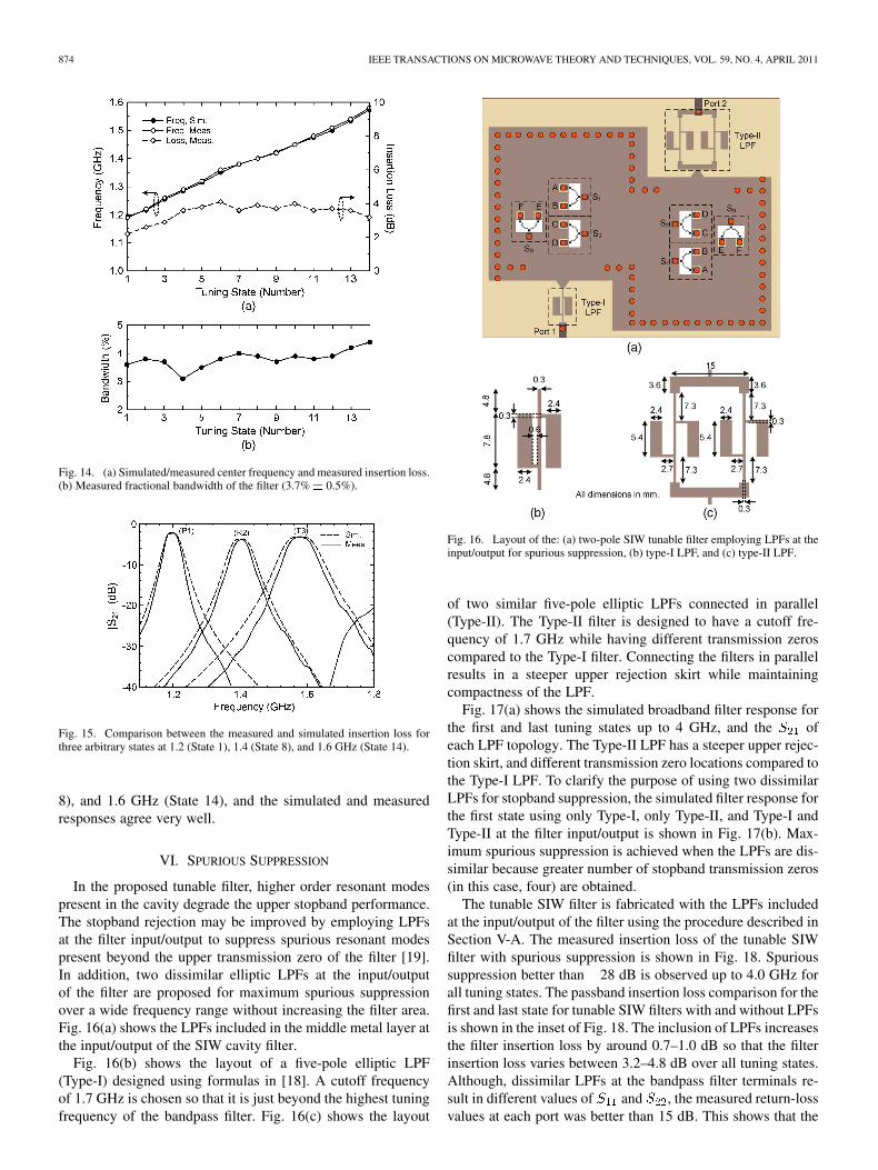
Fig. 14(a) shows the simulated/measured center frequencyand measured insertion loss for each filter response. The sim-ulated and measured center frequencies from 1.2 to 1.6 GHzare in very good agreement. The center frequency variation of1.2–1.6 GHz is equivalent to 28% tuning range with respectto 1.4 GHz. The measured frequency response shows aranging from 93 to 132 with associated insertion losses between2.2–4.1 dB for all tuning states. The filter has lowest insertionloss when all switches are in the up-state position, and theloss increases as more switches are in the down-state position.However, the maximum measured insertion loss correspondsto state 6 (config: ) although state 14 (config: ) hasthe lowest value (Fig. 9), and is attributed to higher filterfractional bandwidth at state 14 compared to state 6.
Fig. 14(b) shows the measured fractional bandwidth, whichvaries between 3.7% 0.5% for all responses. The rela-tively constant fractional bandwidth is obtained by placingtuning posts in regions within the cavity where the externalquality factor shows relatively less variation, as explained inSection III-B. Fig. 15 compares the measured and simulatedinsertion loss for three arbitrary states at 1.2 (State 1), 1.4 (State
874 IEEE TRANSACTIONS ON MICROWAVE THEORY AND TECHNIQUES, VOL. 59, NO. 4, APRIL 2011
Fig. 14. (a) Simulated/measured center frequency and measured insertion loss.(b) Measured fractional bandwidth of the filter (3.7% � 0.5%).
Fig. 15. Comparison between the measured and simulated insertion loss forthree arbitrary states at 1.2 (State 1), 1.4 (State 8), and 1.6 GHz (State 14).
8), and 1.6 GHz (State 14), and the simulated and measuredresponses agree very well.
VI. SPURIOUS SUPPRESSION
In the proposed tunable filter, higher order resonant modespresent in the cavity degrade the upper stopband performance.The stopband rejection may be improved by employing LPFsat the filter input/output to suppress spurious resonant modespresent beyond the upper transmission zero of the filter [19].In addition, two dissimilar elliptic LPFs at the input/outputof the filter are proposed for maximum spurious suppressionover a wide frequency range without increasing the filter area.Fig. 16(a) shows the LPFs included in the middle metal layer atthe input/output of the SIW cavity filter.
Fig. 16(b) shows the layout of a five-pole elliptic LPF(Type-I) designed using formulas in [18]. A cutoff frequencyof 1.7 GHz is chosen so that it is just beyond the highest tuningfrequency of the bandpass filter. Fig. 16(c) shows the layout
Fig. 16. Layout of the: (a) two-pole SIW tunable filter employing LPFs at theinput/output for spurious suppression, (b) type-I LPF, and (c) type-II LPF.
of two similar five-pole elliptic LPFs connected in parallel(Type-II). The Type-II filter is designed to have a cutoff fre-quency of 1.7 GHz while having different transmission zeroscompared to the Type-I filter. Connecting the filters in parallelresults in a steeper upper rejection skirt while maintainingcompactness of the LPF.
Fig. 17(a) shows the simulated broadband filter response forthe first and last tuning states up to 4 GHz, and the ofeach LPF topology. The Type-II LPF has a steeper upper rejec-tion skirt, and different transmission zero locations compared tothe Type-I LPF. To clarify the purpose of using two dissimilarLPFs for stopband suppression, the simulated filter response forthe first state using only Type-I, only Type-II, and Type-I andType-II at the filter input/output is shown in Fig. 17(b). Max-imum spurious suppression is achieved when the LPFs are dis-similar because greater number of stopband transmission zeros(in this case, four) are obtained.
The tunable SIW filter is fabricated with the LPFs includedat the input/output of the filter using the procedure described inSection V-A. The measured insertion loss of the tunable SIWfilter with spurious suppression is shown in Fig. 18. Spurioussuppression better than 28 dB is observed up to 4.0 GHz forall tuning states. The passband insertion loss comparison for thefirst and last state for tunable SIW filters with and without LPFsis shown in the inset of Fig. 18. The inclusion of LPFs increasesthe filter insertion loss by around 0.7–1.0 dB so that the filterinsertion loss varies between 3.2–4.8 dB over all tuning states.Although, dissimilar LPFs at the bandpass filter terminals re-sult in different values of and , the measured return-lossvalues at each port was better than 15 dB. This shows that the

SEKAR et al.: 1.2–1.6-GHz SIW RF MEMS TUNABLE FILTER 875
Fig. 17. (a) Simulated wideband response of the tunable filter and lowpass re-sponses of Type-I and Type-II filters. (b) Spurious suppression for the lowesttuning state for various combinations of LPFs.
Fig. 18. Measured wideband response of the 1.2–1.6-GHz tunable SIW filterwith spurious suppression.
filter can still be used as a symmetric two-port network withoutaffecting system performance.
VII. NONLINEAR CHARACTERIZATION
The third-order intermodulation components of the tunablefilters with and without LPFs were measured using a setup sim-ilar to the one shown in [20]. For a particular tuning state, a two-tone signal was applied to each tunable filter within the filterpassband with a separation frequency of 10 kHz (or 1 MHz), andthe third-order intermodulation products were measured using a
spectrum analyzer. Due to the extremely linear behavior of theRF MEMS switches, the third-order intermodulation level wasalways below the noise level of the Agilent E4446A spectrumanalyzer as long as the RF mixer of the spectrum analyzer wasnot saturated by the input signal (a maximum power of 15 dBmwas used). As a result, it was impossible to measure the ofthe tunable filters for any tuning state. Thus, it can be concludedthat the of the RF MEMS tunable filters is 65 dBm, whichis an incredible number compared to other tuning technologiessuch as p-i-n diodes.
For comparison, intermodulation components of the tunableSIW filter employing p-i-n diodes developed earlier by the au-thors [11] was measured. For a two-tone signal with 10-kHzbeat frequency, the worst case measured for this filter was25 dBm when all p-i-n diodes were reverse biased. The worstcase was also measured for various beat frequencies (up to1 MHz), and remained approximately constant.
Although resistance variations in metal-contact MEMSswitches result in intermodulation distortion, the of suchMEMS switches due to this mechanism is calculated to bearound 80 dBm [22]. As a result, the intermodulation prod-ucts in circuits employing metal-contact RF MEMS switchesare very hard to measure.
VIII. CONCLUSION
This paper has demonstrated an SIW RF MEMS tunablefilter with a tuning range of 1.2–1.6 GHz employing packagedRF MEMS switches. The measured filter of 93–132 is thehighest reported in filters using off-the-shelf RF MEMSswitches on conventional PCB substrates. Out-of-band inter-ference is greatly reduced by including LPFs at the bandpassfilter terminals for improved upper stopband rejection. Sincefabrication of this filter only requires conventional PCB pro-cesses, the manufacturing cost is significantly lower. Successfulimplementation of this filter proves that commercialization ofRF MEMS switch technology as off-the-shelf components willbe highly useful in developing low-cost tunable filters with lowloss, wide tuning, and very high linearity.
REFERENCES
[1] G. M. Rebeiz, K. Entesari, I. Reines, S.-J. Park, M. El-Tanani, A. Grich-ener, and A. Brown, “Tuning in to RF MEMS,” in IEEE MTT-S Int.Microw. Symp. Dig., Oct. 2009, vol. 10, no. 6, pp. 55–72.
[2] S.-J. Park, K.-Y. Lee, and G. M. Rebeiz, “Low-loss 5.15–5.70 GHzRF MEMS switchable filter for wireless WLAN applications,” IEEETrans. Microw. Theory Tech., vol. 54, no. 11, pp. 3931–3939, Nov.2006.
[3] S.-J. Park, I. Reines, and G. M. Rebeiz, “Low-loss 4–6 GHz tunablefilter with 3-bit high-� orthogonal bias RF MEMS capacitancenetwork,” IEEE Trans. Microw. Theory Tech., vol. 56, no. 10, pp.2348–2355, Oct. 2008.
[4] M. A. El-Tanani and G. M. Rebeiz, “High-performance 1.5–2.5 GHzRF MEMS tunable filters for wireless applications,” IEEE Trans. Mi-crow. Theory Tech., vol. 58, no. 6, pp. 1629–1637, Jun. 2010.
[5] S.-J. Park, I. Reines, C. Patel, and G. M. Rebeiz, “High-� RF MEMS4–6 GHz tunable evanescent-mode cavity filter,” IEEE Trans. Microw.Theory Tech., vol. 58, no. 2, pp. 381–389, Feb. 2010.
[6] K. Entesari and G. M. Rebeiz, “A 25–75-MHz RF MEMS tun-able filter,” IEEE Trans. Microw. Theory Tech., vol. 55, no. 11, pp.2399–2405, Nov. 2007.
[7] V. Sekar and K. Entesari, “Inductively-loaded RF MEMS reconfig-urable filters,” Int. J. RF Microw. Comput.-Aided Eng., vol. 19, no. 6,pp. 692–700, Dec. 2009.

876 IEEE TRANSACTIONS ON MICROWAVE THEORY AND TECHNIQUES, VOL. 59, NO. 4, APRIL 2011
[8] D. Deslandes and K. Wu, “Single-substrate integration technique ofplanar circuits and waveguide filters,” IEEE Trans. Microw. TheoryTech., vol. 51, no. 2, pp. 593–596, Feb. 2003.
[9] X.-P. Chen, K. Wu, and D. Drolet, “Substrate integrated waveguidefilter with improved stopband performance for satellite ground ter-minal,” IEEE Trans. Microw. Theory Tech., vol. 57, no. 3, pp. 674–683,Mar. 2009.
[10] J. C. Bohorquez, B. Potelon, C. Person, E. Rius, C. Quendo, G. Tanne,and E. Fourn, “Reconfigurable planar SIW cavity resonator and filter,”in IEEE MTT-S Int. Microw. Symp. Dig., San Francisco, CA, Jun. 2006,pp. 947–950.
[11] M. Armendariz, V. Sekar, and K. Entesari, “Tunable SIW bandpassfilters with PIN diodes,” in 40th Eur. Microw. Conf., Paris, France, Sep.28–30, 2010, pp. 830–833.
[12] W. Gautier, A. Stehle, B. Schoenlinner, V. Ziegler, U. Prechtel, andW. Menzel, “RF MEMS tunable filters on low-loss LTCC substratefor UAV data-link,” in Proc. 4th Eur. Microw. Integr. Circuits Conf.,Rome, Italy, Sep. 28–29, 2009, pp. 347–350.
[13] K. Wu, D. Deslandes, and Y. Cassivi, “The substrate integrated cir-cuits—A new concept for high-frequency electronics and optoelec-tronics,” in 6th Int. Telecommun. Modern Satellite, Cable Broadcast.Service Conf. , Oct. 1–3, 2003, vol. 1, pp. P-III–P-X.
[14] S. Amari and U. Rosenberg, “Characteristics of cross (bypass) cou-pling through higher/lower order modes and their applications in el-liptic filter design,” IEEE Trans. Microw. Theory Tech., vol. 53, no. 10,pp. 3135–3141, Oct. 2005.
[15] Y. Uno, K. Narise, T. Masuda, K. Inoue, Y. Adachi, K. Hosoya, T. Seki,and F. Sato, “Development of SPDT-structured RF MEMS switch,” in15th Int. Solid-State Sens., Actuators Microsyst. Conf., Denver, CO,Jun. 21–25, 2009, pp. 541–544.
[16] T. Seki, F. Sato, T. Masuda, I. Kimura, and K. Imanaka, “Low-lossRF MEMS metal-to-metal contact switch with CSP structure,” in 12thInt. Solid-State Sensors, Actuators Microsyste. Conf., Boston, MA, Jun.9–12, 2003, vol. 1, pp. 340–341.
[17] N. Marcuvitz, Waveguide Handbook. New York: Dover, 1951.[18] J. S. Hong and M. J. Lancaster, Microstrip Filters For RF/Microwave
Applications. New York: Wiley, 2001.[19] T.-S. Yun, H. Nam, J.-Y. Kim, B. Lee, J.-J. Choi, K.-B. Kim, T.-J. Ha,
and J.-C. Lee, “Harmonics suppressed substrate-integrated-waveguidefilter with integration of low-pass filter,” Microw. Opt. Technol. Lett.,vol. 50, pp. 447–450, Jan. 2008.
[20] K. Entesari and G. M. Rebeiz, “A 12-18-GHz three-pole RF MEMStunable filter,” IEEE Trans. Microw. Theory Tech., vol. 53, no. 8, pp.2566–2571, Aug. 2005.
[21] G. M. Rebeiz, RF MEMS Theory, Design and Technology. New York:Wiley, 2003.
[22] J. Johnson, G. G. Adams, and N. E. McGruer, “Determination of in-termodulation distortion in a contact-type MEMS microswitch,” IEEETrans. Microw. Theory Tech., vol. 53, no. 8, pp. 2566–2571, Aug. 2005.
Vikram Sekar (S’07) received the Bachelors degreein electrical engineering from Visveswariah Tech-nological University, Belgaum, India, in 2006, theM.S. degree in electrical engineering from TexasA&M University, College Station, in 2008, andis currently working toward the Ph.D. degree inelectrical engineering at Texas A&M University.
During the summers of 2007 and 2008, he was anIntern with Texas Instruments Incorporated, Dallas,TX, where he was involved with signal integrityissues and system-level electromagnetic analysis
of printed-circuit boards for wireless handsets. From 2008 to 2009, he wasa Teaching Assistant with the Department of Electrical Engineering, TexasA&M University. His research interests include fixed-frequency and tunablemicrowave filters, nonlinearity and noise in tunable filters, RF MEMS, andmicrowave sensors.
Marcelino Armendariz (M’10) received the B.S.degree in electrical engineering from the UnitedStates Air Force Academy, Colorado Springs, CO, in2000, and the M.S. degree in electrical engineeringfrom Texas A&M University, College Station, in2010.
From 2000 to 2007, he served in the UnitedStates military as an Electronic Warfare Pilot and anInstructor Pilot for the Air Education and TrainingCommand. From 2008 to 2010, he was a TeachingAssistant with the Department of Electrical Engi-
neering, Texas A&M University. He is currently a Senior RF Engineer withSpace and Airborne Systems, Raytheon, Dallas, TX. His research interestsinclude tunable microwave filters, passive RF components, and microelectroniccircuit fabrication.
Kamran Entesari (S’03–M’06) received the B.S.degree in electrical engineering from the SharifUniversity of Technology, Tehran, Iran, in 1995, theM.S. degree in electrical engineering from TehranPolytechnic University, Tehran, Iran, in 1999, andthe Ph.D. degree from The University of Michiganat Ann Arbor, in 2005.
In 2006, he joined the Department of Electricaland Computer Engineering, Texas A&M University,College Station, where he is currently an AssistantProfessor. His research interests include design of
RF/microwave/millimeter-wave integrated circuits and systems, RF MEMS,and medical electronics.
Dr. Entesari was the recipient of the 2011 National Science Foundation (NSF)CAREER Award. He was the corecipient of the 2009 Semiconductor ResearchCorporation (SRC) Design Contest Second Project Award for his work on dual-band millimeter-wave receivers on silicon.