Embed Size (px)
Citation preview
Disclaimer: This course was prepared, in its entirety, by Adam Teman. Many materials were copied from sources freely available on the internet. When possible, these sources have been cited;
however, some references may have been cited incorrectly or overlooked. If you feel that a picture, graph, or code example has been copied from you and either needs to be cited or removed,
please feel free to email [email protected] and I will address this as soon as possible.
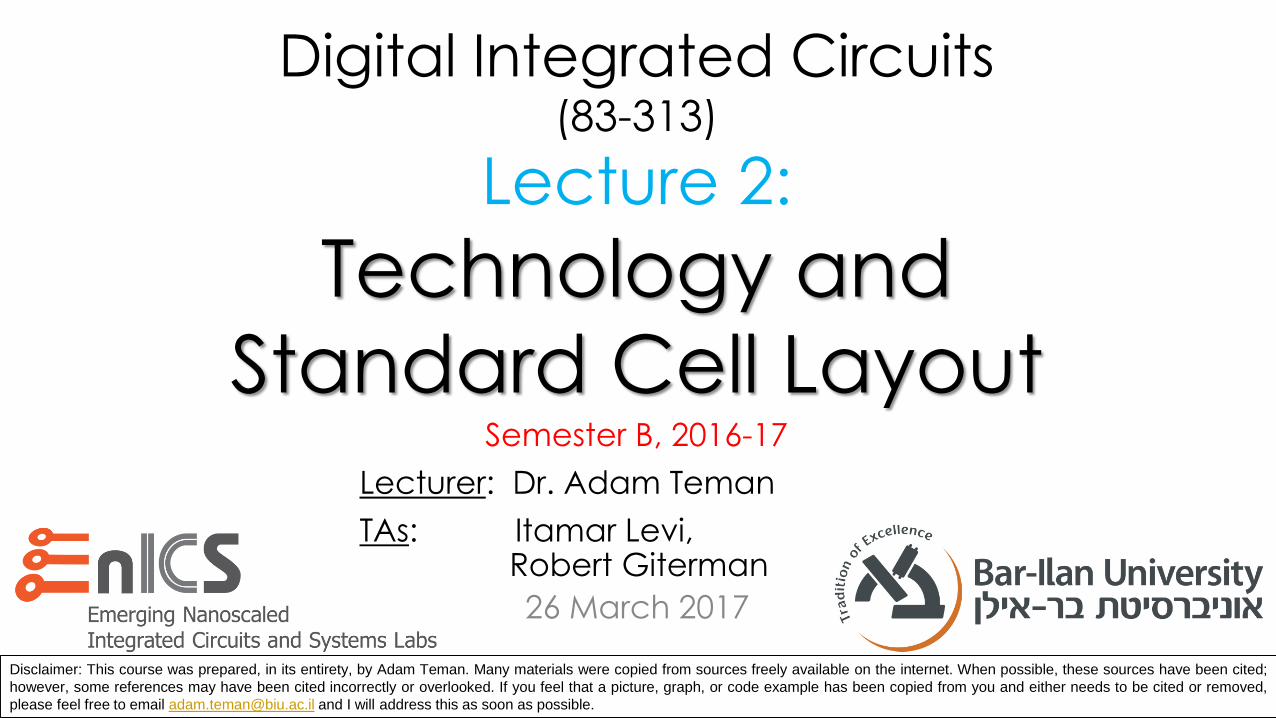
Digital Integrated Circuits(83-313)
Lecture 2:
Technology and
Standard Cell LayoutSemester B, 2016-17
Lecturer: Dr. Adam Teman
TAs: Itamar Levi, Robert Giterman
26 March 2017
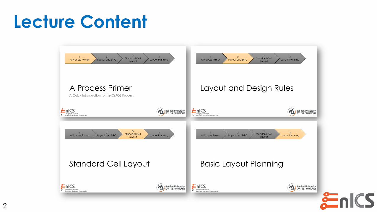
Lecture Content
2
A Process PrimerA Quick Introduction to the CMOS Process
3
1
A Process Primer
2
Layout and DRC
4
Layout Planning
3
Standard Cell
Layout
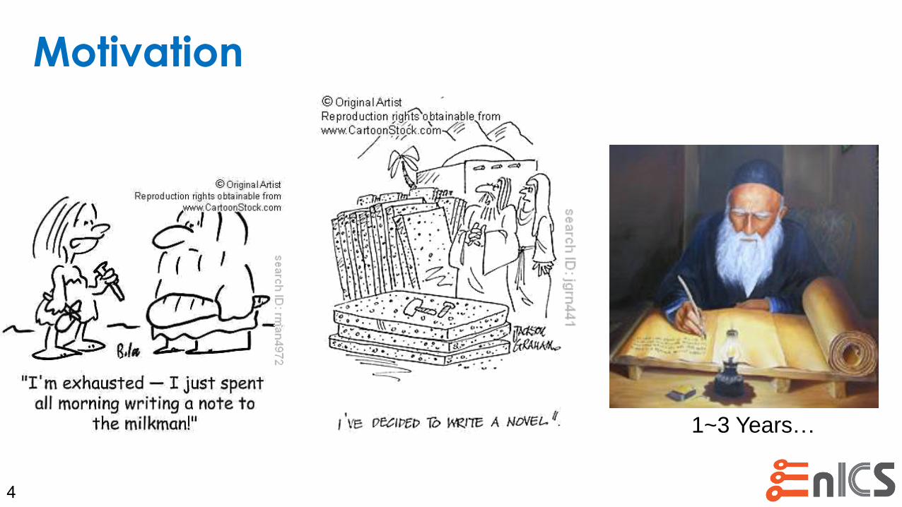
Motivation
4
1~3 Years…
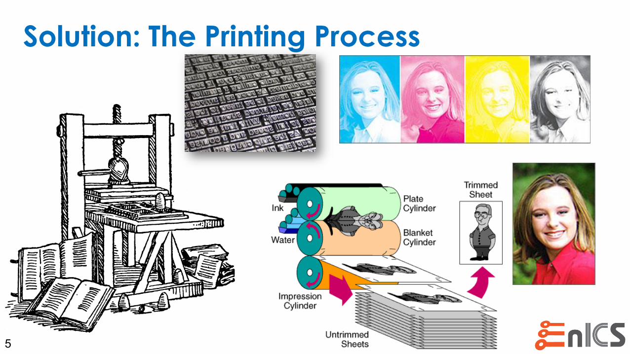
Solution: The Printing Process
5
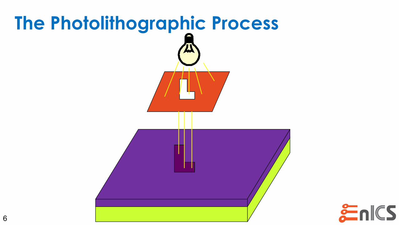
The Photolithographic Process
6
CMOS Process/Transistors
7
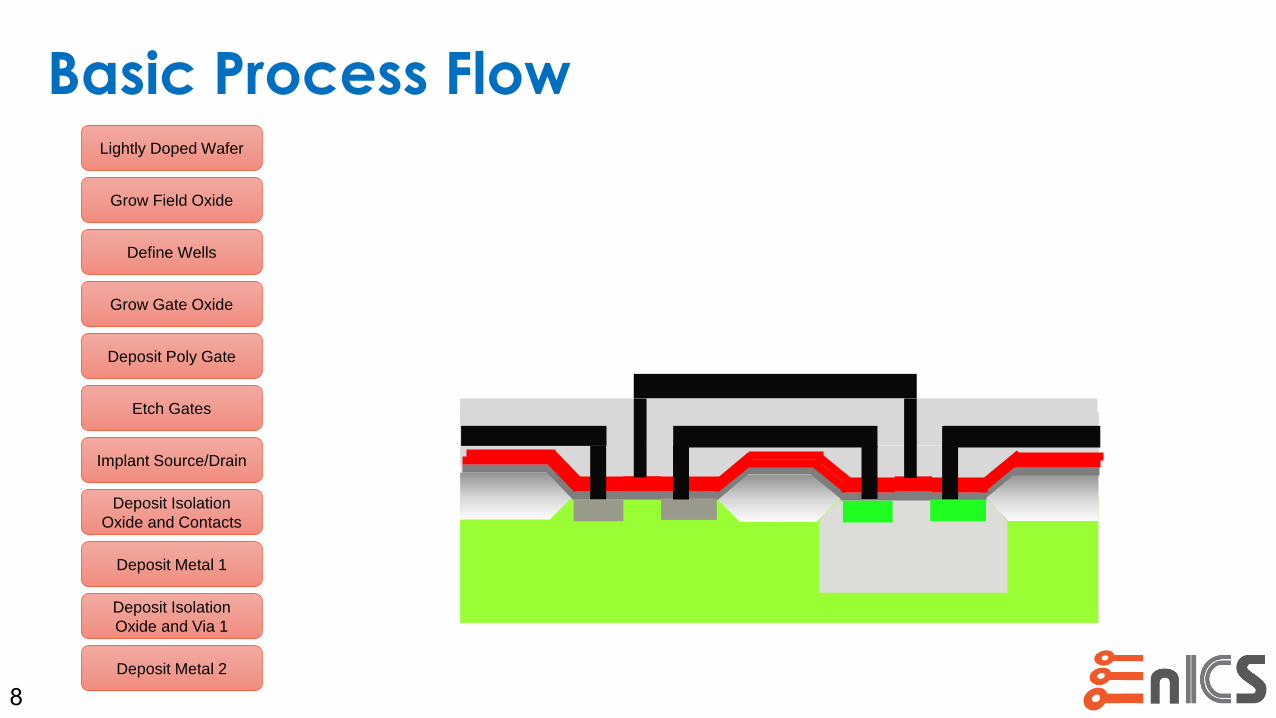
Basic Process Flow
8
Lightly Doped Wafer
Grow Field Oxide
Define Wells
Grow Gate Oxide
Deposit Poly Gate
Etch Gates
Implant Source/Drain
Deposit Isolation
Oxide and Contacts
Deposit Metal 1
Deposit Isolation
Oxide and Via 1
Deposit Metal 2
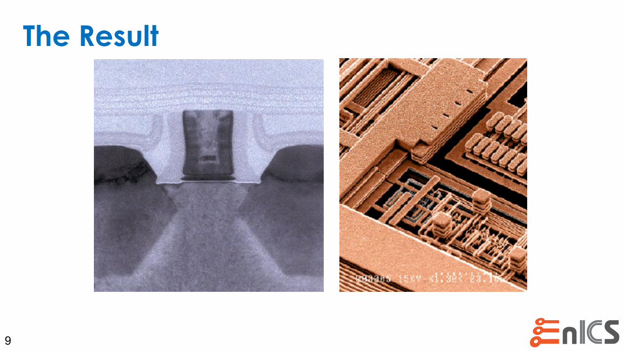
The Result
9
Layout and Design Rules
10
1
A Process Primer
2
Layout and DRC
4
Layout Planning
3
Standard Cell
Layout
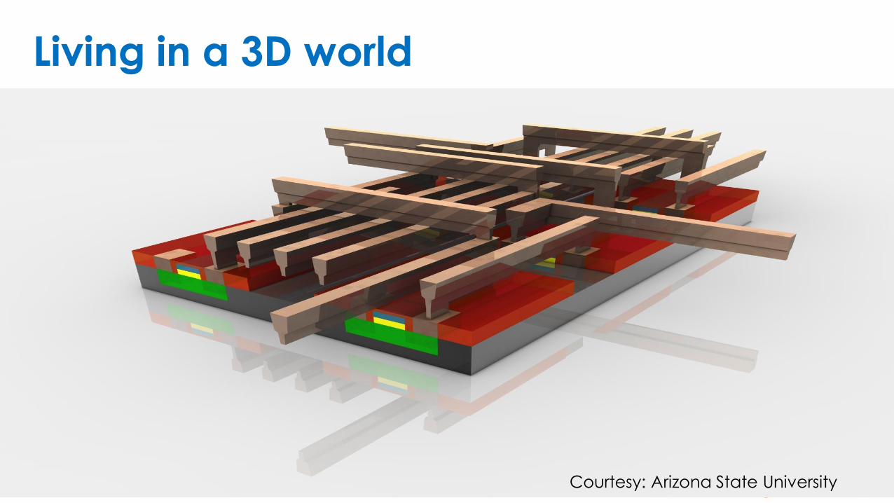
Living in a 3D world
11 Courtesy: Arizona State University
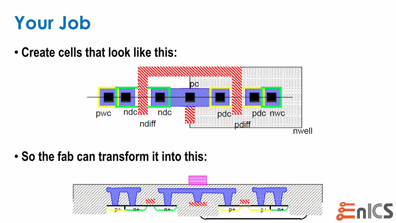
Your Job
• Create cells that look like this:
• So the fab can transform it into this:
12
How do we layout a transistor?
13
The Design Rule Manual
• Design Rules (also known as DRCs), are the interface between the
designer and process engineer.• The Design Rule Manual (DRM) provides guidelines for constructing process
masks.
• These are generally categorized as:• Intra-layer rules: minimum widths, spacing,
area, etc., only relating to a single layer.
• Inter-layer rules: minimum enclosures,
extensions, overlaps, etc., between two layers.
• Special rules: non geometric rules, such as
antenna rules, density, distance to welltap, etc.
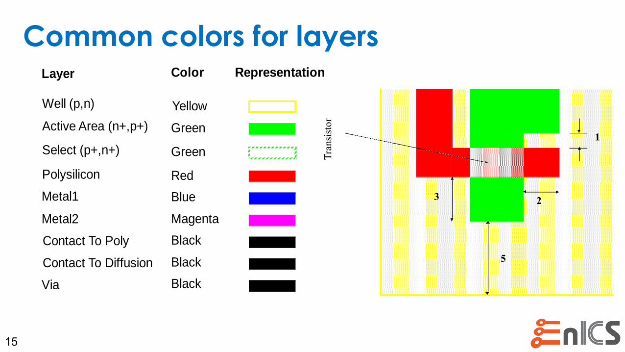
Common colors for layers
15
Layer
Polysilicon
Metal1
Metal2
Contact To Poly
Contact To Diffusion
Via
Well (p,n)
Active Area (n+,p+)
Color Representation
Yellow
Green
Red
Blue
Magenta
Black
Black
Black
Select (p+,n+) Green
1
2
5
3
Transistor
Layer
Polysilicon
Metal1
Metal2
Contact To Poly
Contact To Diffusion
Via
Well (p,n)
Active Area (n+,p+)
Color Representation
Yellow
Green
Red
Blue
Magenta
Black
Black
Black
Select (p+,n+) Green
Layer
Polysilicon
Metal1
Metal2
Contact To Poly
Contact To Diffusion
Via
Well (p,n)
Active Area (n+,p+)
Color Representation
Yellow
Green
Red
Blue
Magenta
Black
Black
Black
Select (p+,n+) Green
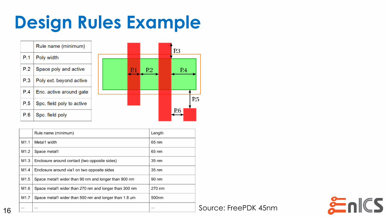
Design Rules Example
16 Source: FreePDK 45nm
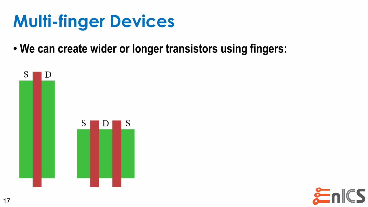
Multi-finger Devices
• We can create wider or longer transistors using fingers:
17
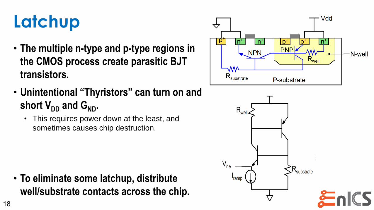
Latchup
• The multiple n-type and p-type regions in
the CMOS process create parasitic BJT
transistors.
• Unintentional “Thyristors” can turn on and
short VDD and GND.• This requires power down at the least, and
sometimes causes chip destruction.
• To eliminate some latchup, distribute
well/substrate contacts across the chip.18
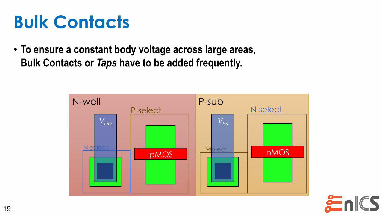
Bulk Contacts
• To ensure a constant body voltage across large areas,
Bulk Contacts or Taps have to be added frequently.
19
N-well P-subP-select N-select
pMOS nMOSN-select P-select
VDD VSS
Standard Cell Layout
20
1
A Process Primer
2
Layout and DRC
4
Layout Planning
3
Standard Cell
Layout
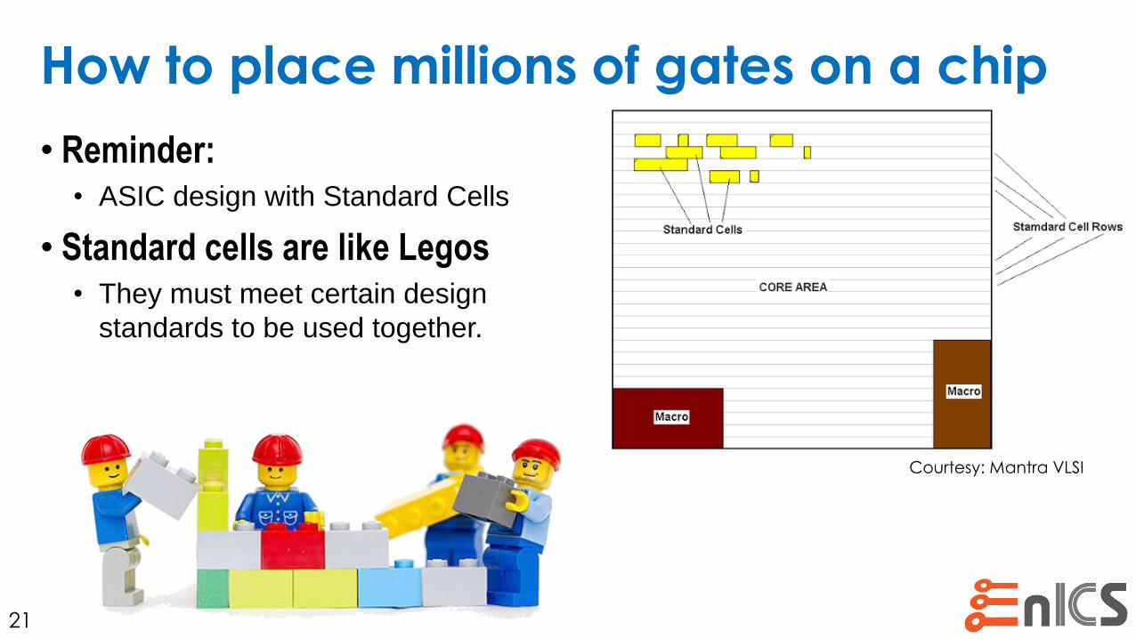
How to place millions of gates on a chip
• Reminder: • ASIC design with Standard Cells
• Standard cells are like Legos• They must meet certain design
standards to be used together.
21
Courtesy: Mantra VLSI
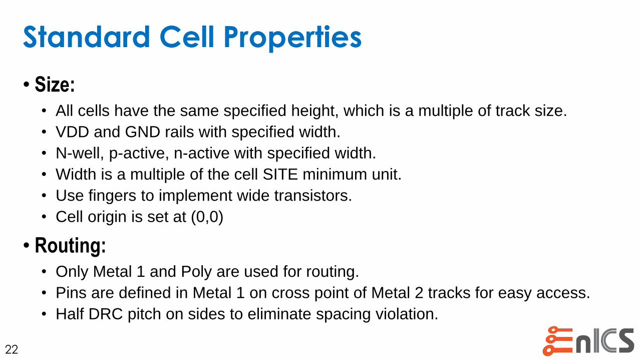
Standard Cell Properties
• Size:• All cells have the same specified height, which is a multiple of track size.
• VDD and GND rails with specified width.
• N-well, p-active, n-active with specified width.
• Width is a multiple of the cell SITE minimum unit.
• Use fingers to implement wide transistors.
• Cell origin is set at (0,0)
• Routing:• Only Metal 1 and Poly are used for routing.
• Pins are defined in Metal 1 on cross point of Metal 2 tracks for easy access.
• Half DRC pitch on sides to eliminate spacing violation.
22
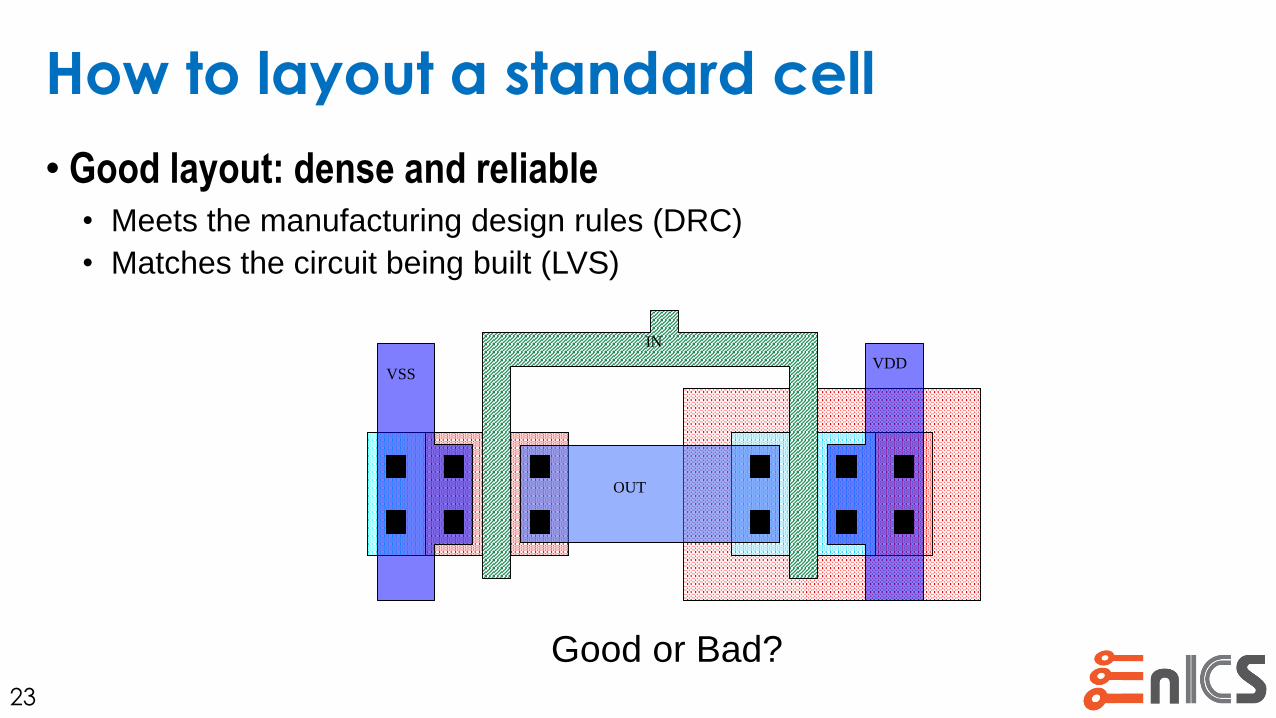
How to layout a standard cell
• Good layout: dense and reliable• Meets the manufacturing design rules (DRC)
• Matches the circuit being built (LVS)
23
VSSVDD
IN
OUT
Good or Bad?
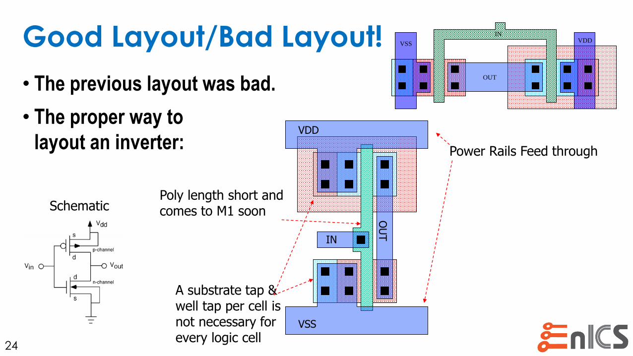
Good Layout/Bad Layout!
• The previous layout was bad.
• The proper way to
layout an inverter:
24
VSS
OU
TIN
VDD
Poly length short and comes to M1 soon
Power Rails Feed through
Schematic
A substrate tap &well tap per cell isnot necessary for every logic cell
VSSVDD
IN
OUT
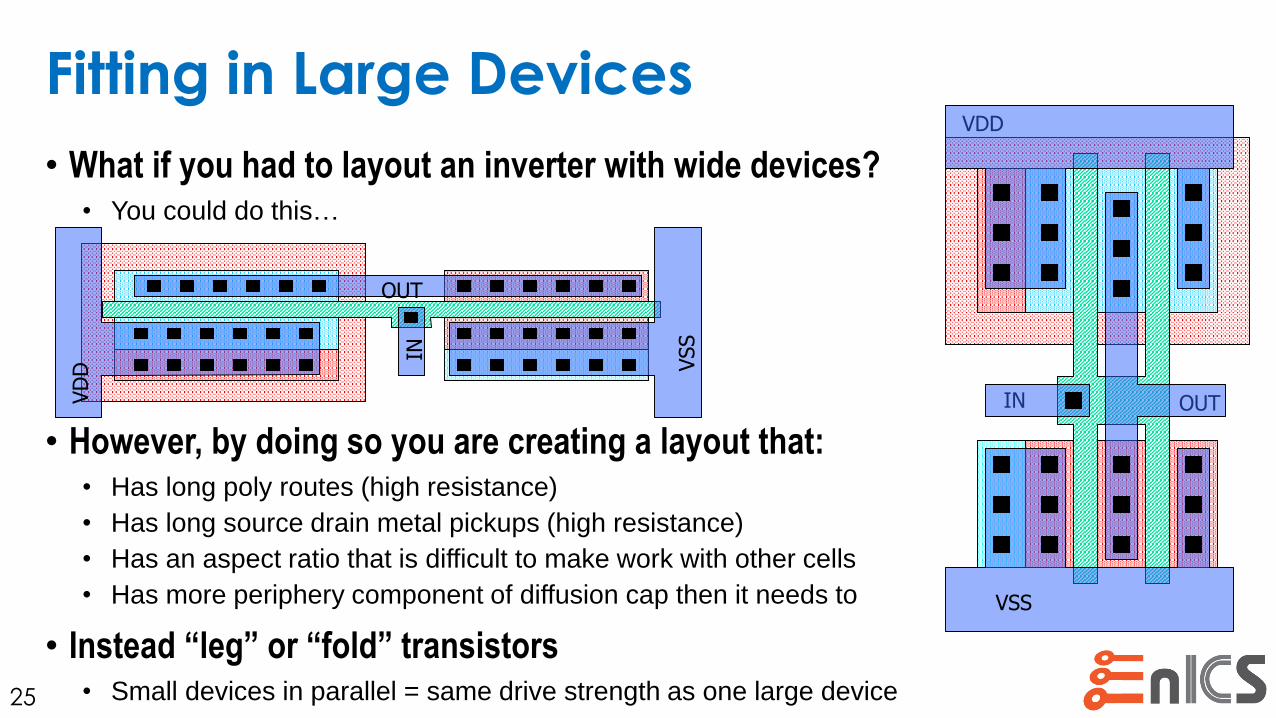
Fitting in Large Devices
• What if you had to layout an inverter with wide devices?• You could do this…
• However, by doing so you are creating a layout that:• Has long poly routes (high resistance)
• Has long source drain metal pickups (high resistance)
• Has an aspect ratio that is difficult to make work with other cells
• Has more periphery component of diffusion cap then it needs to
• Instead “leg” or “fold” transistors• Small devices in parallel = same drive strength as one large device25
VSS
OUT
IN
VD
D
IN
VDD
OUT
VSS
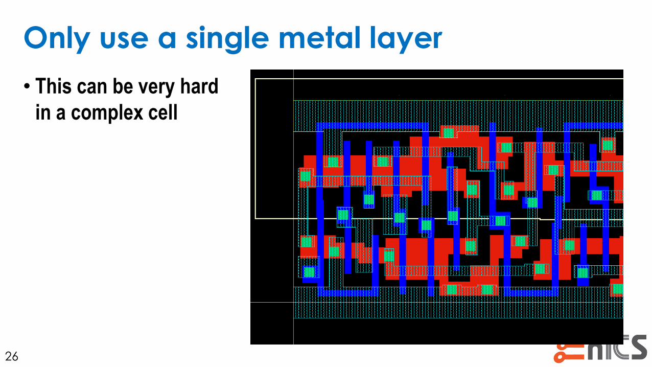
Only use a single metal layer
• This can be very hard
in a complex cell
26
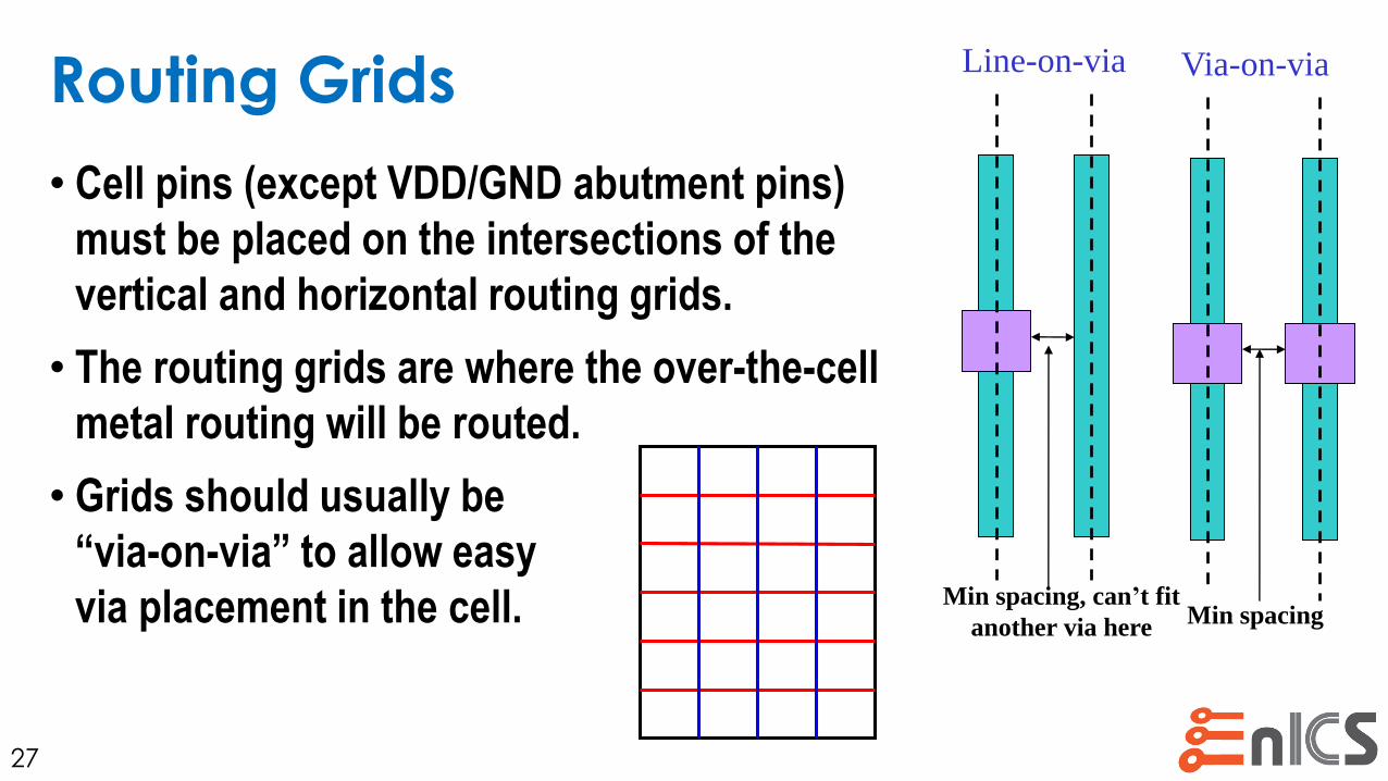
Routing Grids
• Cell pins (except VDD/GND abutment pins)
must be placed on the intersections of the
vertical and horizontal routing grids.
• The routing grids are where the over-the-cell
metal routing will be routed.
• Grids should usually be
“via-on-via” to allow easy
via placement in the cell.
27
Via-on-via
Min spacing
Line-on-via
Min spacing, can’t fit
another via here
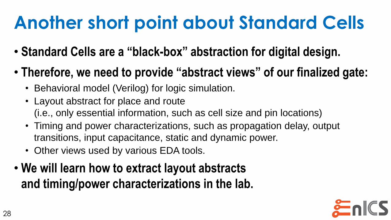
Another short point about Standard Cells
• Standard Cells are a “black-box” abstraction for digital design.
• Therefore, we need to provide “abstract views” of our finalized gate:• Behavioral model (Verilog) for logic simulation.
• Layout abstract for place and route
(i.e., only essential information, such as cell size and pin locations)
• Timing and power characterizations, such as propagation delay, output
transitions, input capacitance, static and dynamic power.
• Other views used by various EDA tools.
• We will learn how to extract layout abstracts
and timing/power characterizations in the lab.
28
Basic Layout Planning
29
1
A Process Primer
2
Layout and DRC
4
Layout Planning
3
Standard Cell
Layout
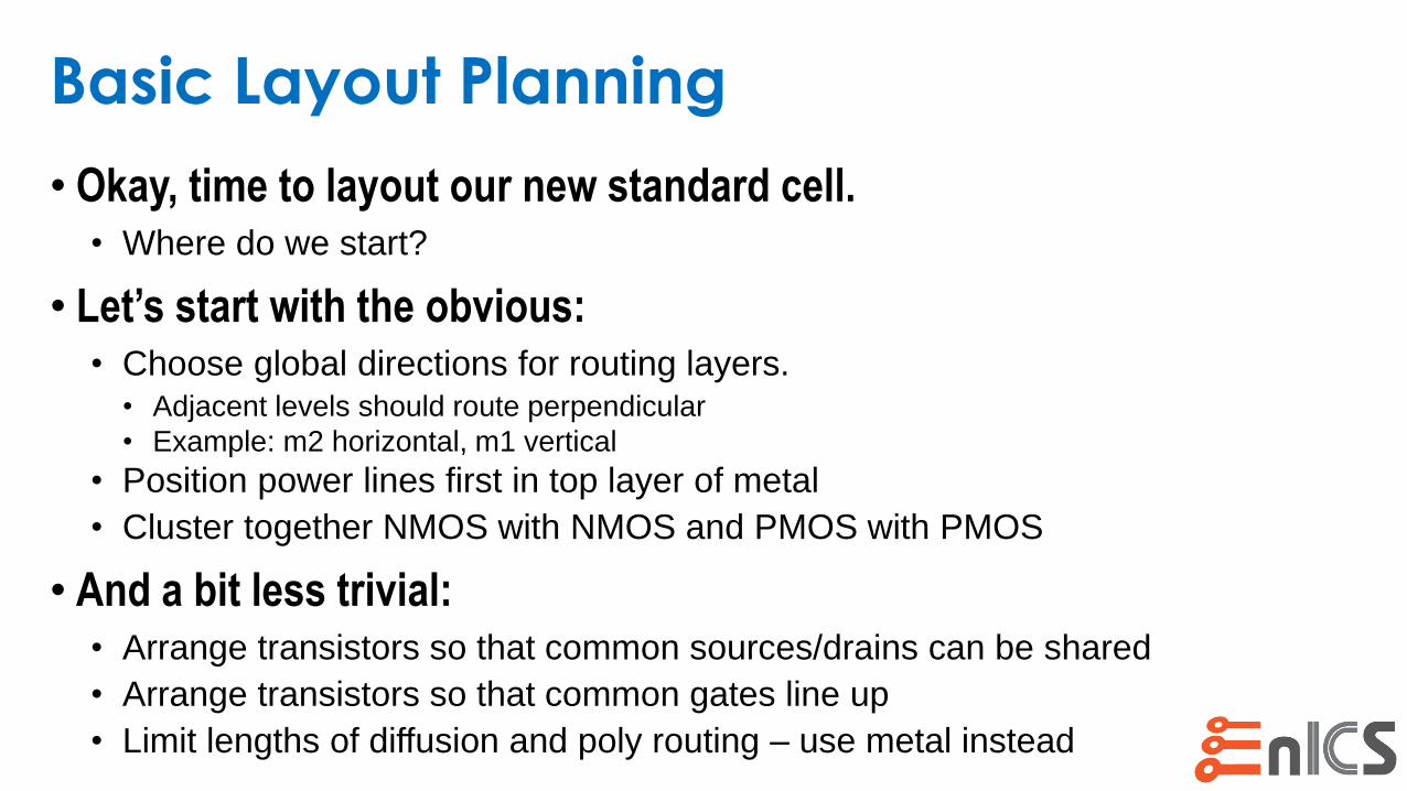
Basic Layout Planning
• Okay, time to layout our new standard cell. • Where do we start?
• Let’s start with the obvious:• Choose global directions for routing layers. • Adjacent levels should route perpendicular
• Example: m2 horizontal, m1 vertical
• Position power lines first in top layer of metal
• Cluster together NMOS with NMOS and PMOS with PMOS
• And a bit less trivial:• Arrange transistors so that common sources/drains can be shared
• Arrange transistors so that common gates line up
• Limit lengths of diffusion and poly routing – use metal instead
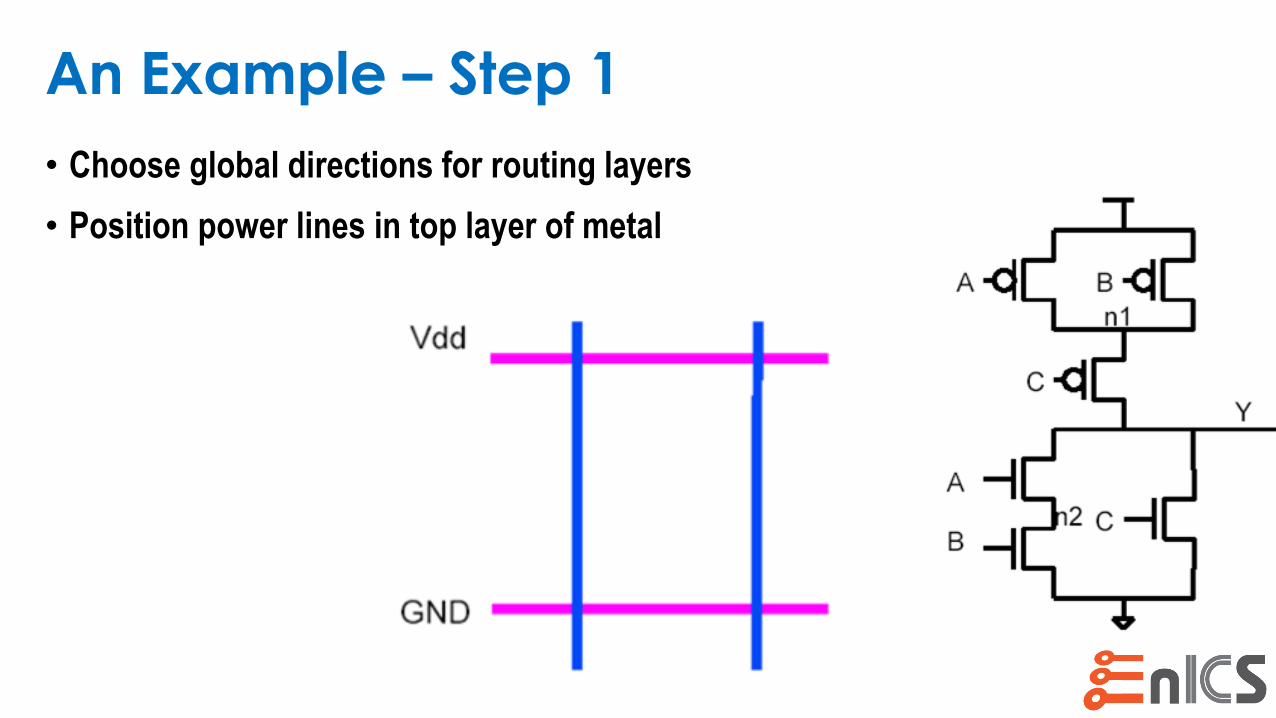
An Example – Step 1
• Choose global directions for routing layers
• Position power lines in top layer of metal
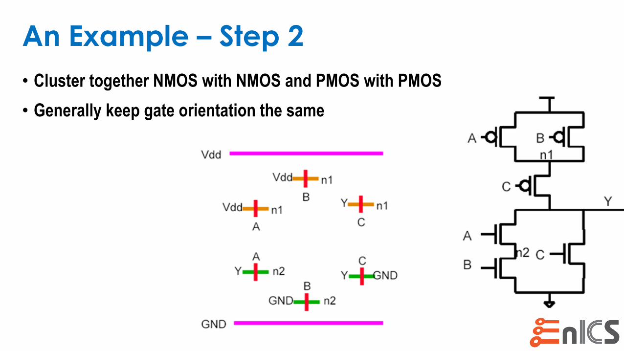
An Example – Step 2
• Cluster together NMOS with NMOS and PMOS with PMOS
• Generally keep gate orientation the same
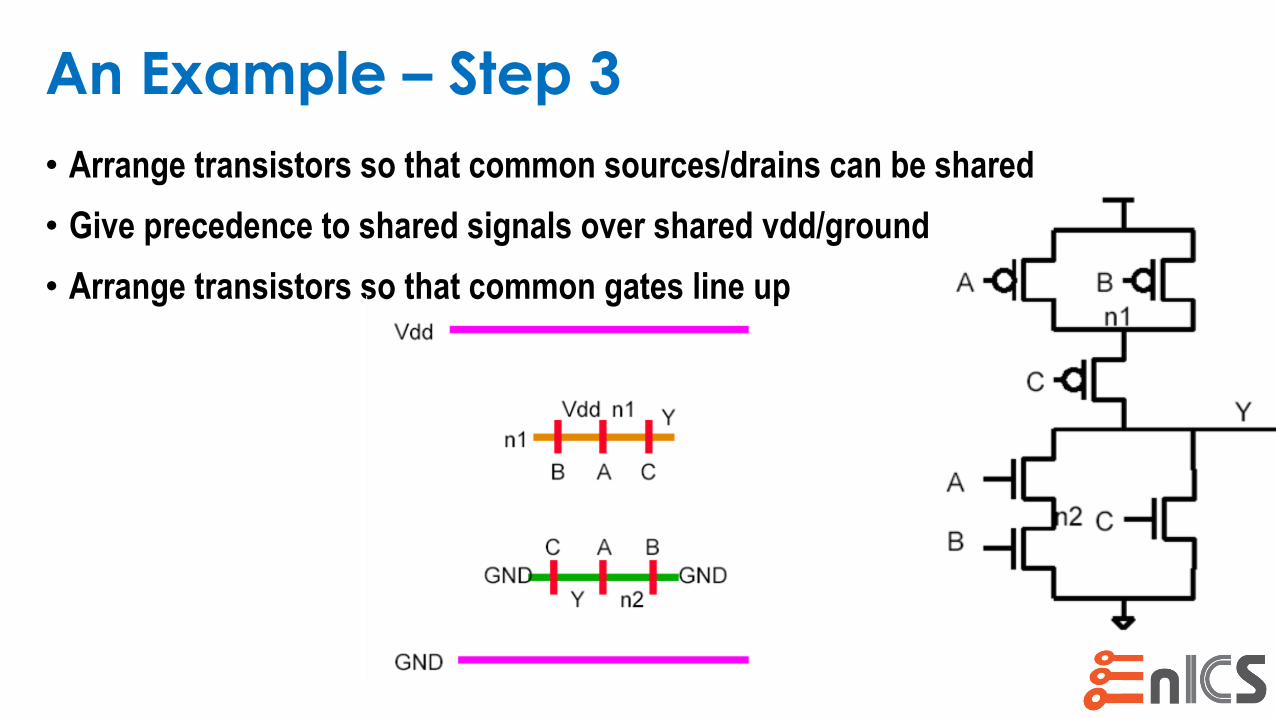
An Example – Step 3
• Arrange transistors so that common sources/drains can be shared
• Give precedence to shared signals over shared vdd/ground
• Arrange transistors so that common gates line up
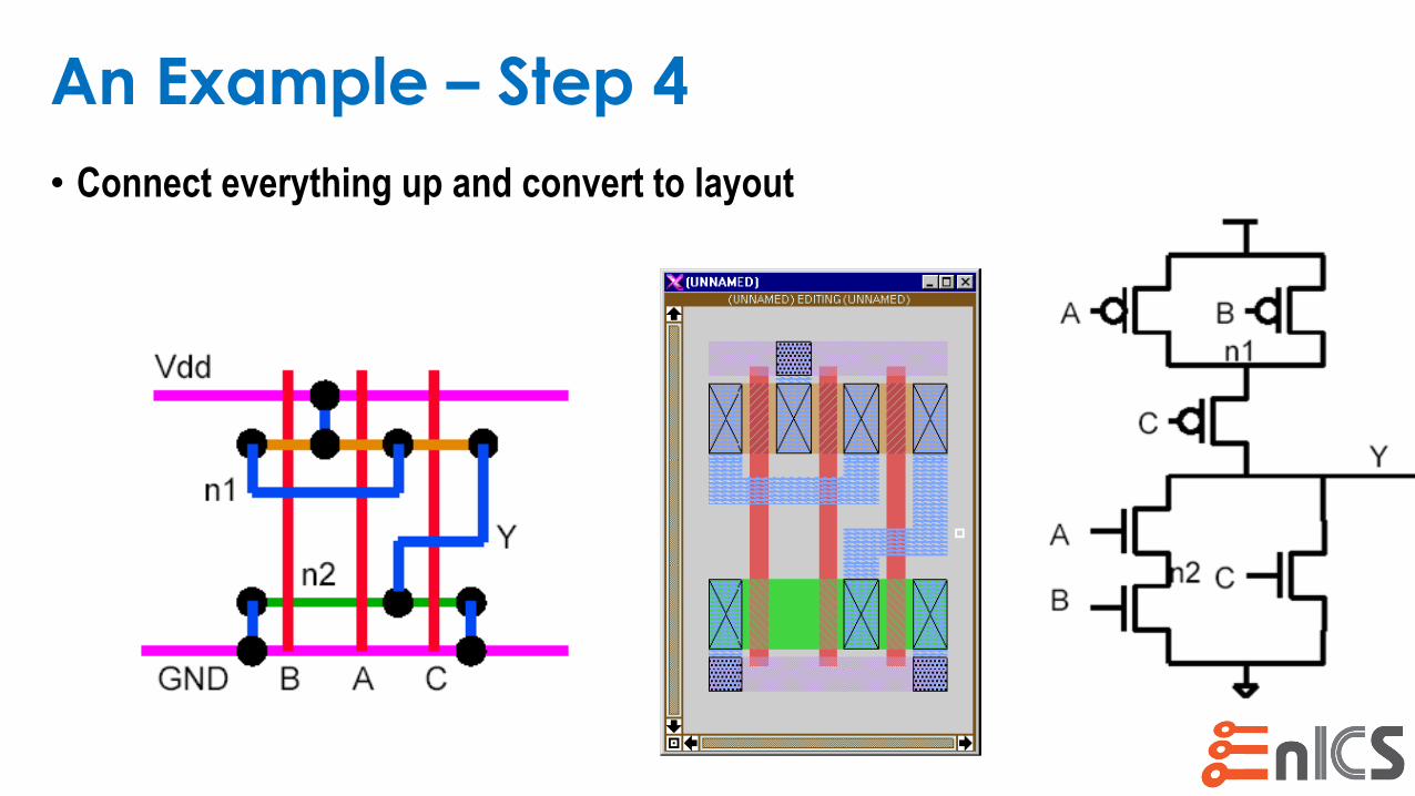
An Example – Step 4
• Connect everything up and convert to layout
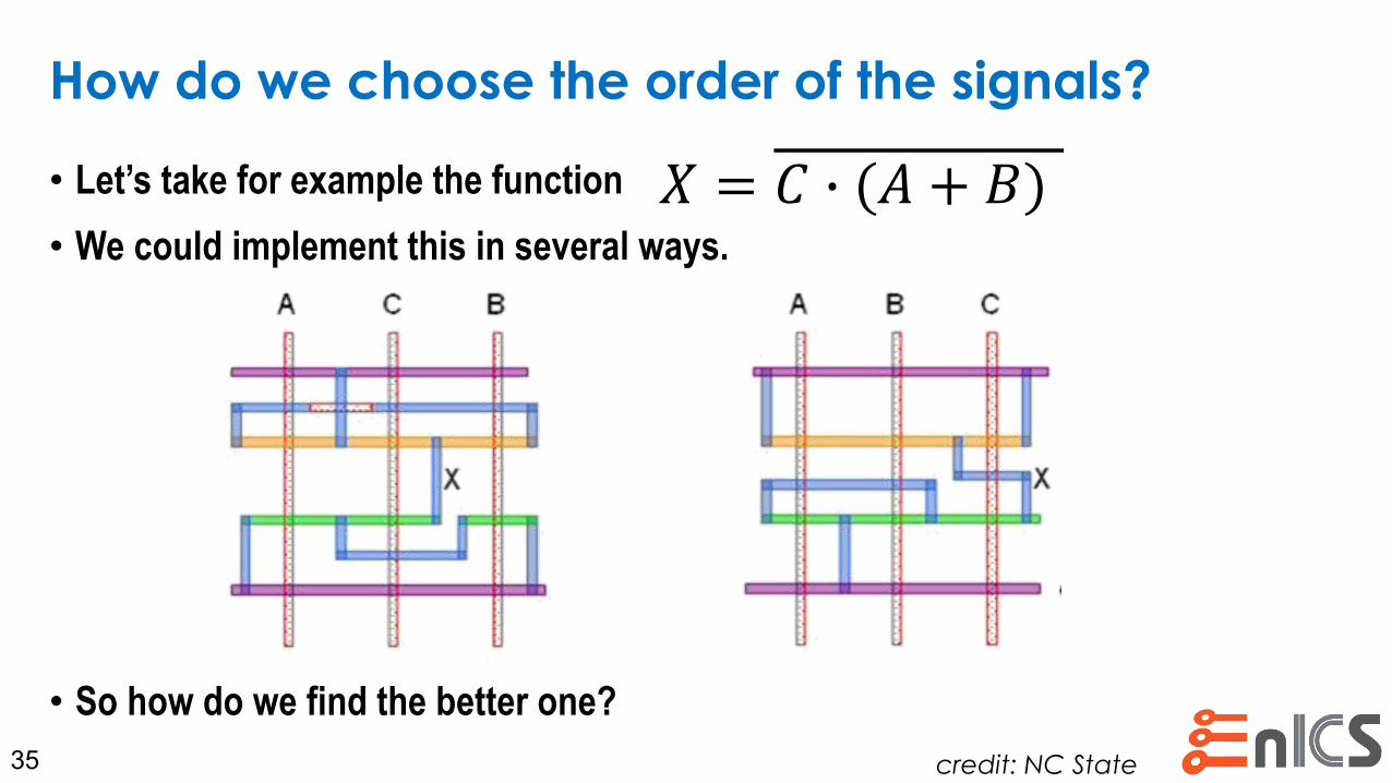
How do we choose the order of the signals?
• Let’s take for example the function
• We could implement this in several ways.
35
𝑋 = 𝐶 ∙ (𝐴 + 𝐵)
• So how do we find the better one?
credit: NC State
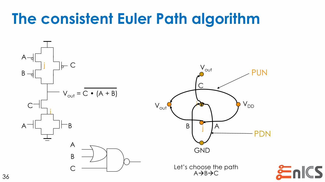
36
j
VDDVout
Vout
i
GND
AB
C
PDN
PUN
B
C
C
A
B
A
i
j
A
B
C
Vout = C • (A + B)
The consistent Euler Path algorithm
Let’s choose the path ABC
The consistent Euler Path algorithm
37
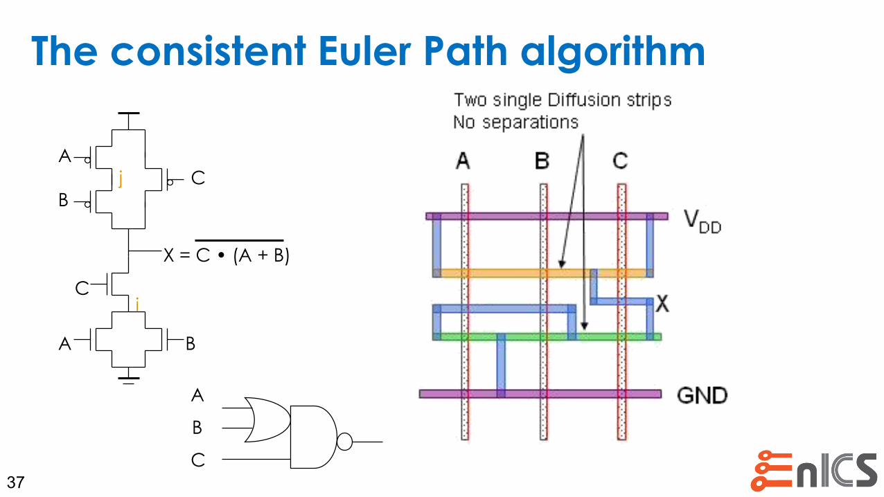
B
C
C
A
B
A
i
j
A
B
C
X = C • (A + B)
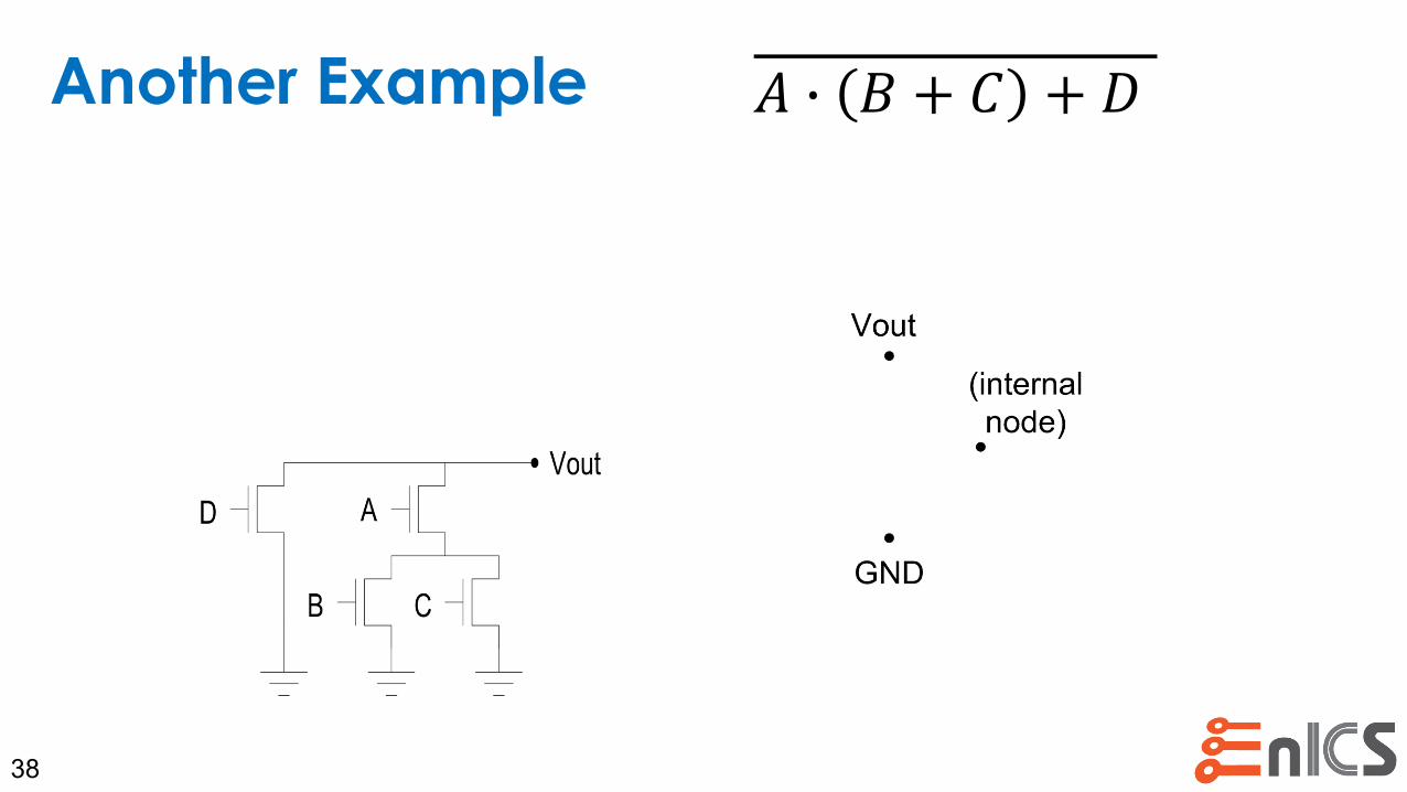
Another Example
38
𝐴 ∙ 𝐵 + 𝐶 + 𝐷
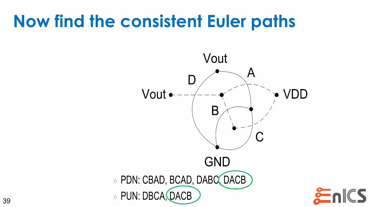
Now find the consistent Euler paths
39
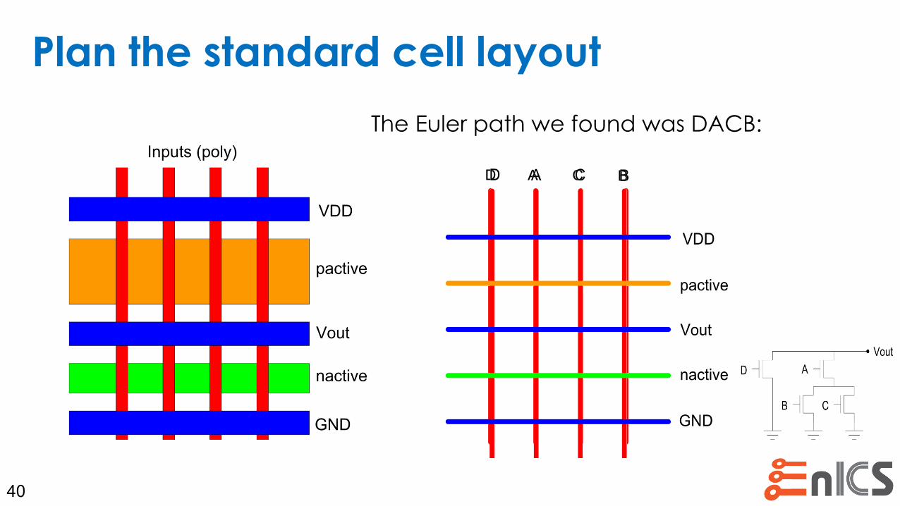
Plan the standard cell layout
40
The Euler path we found was DACB:
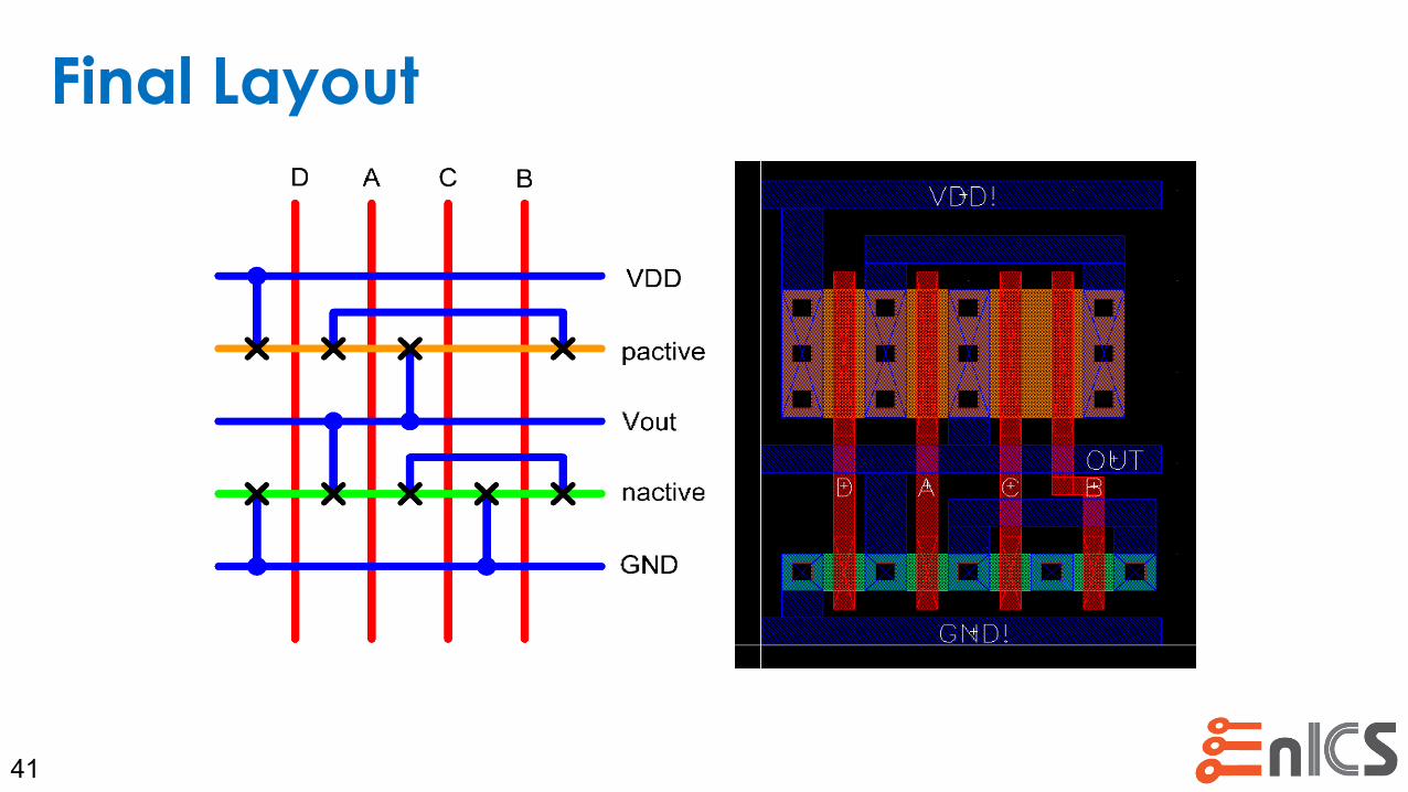
Final Layout
41 Slide 19© W. Rhett Davis NC State University ECE 546 Fall 2012
Then Draw the Layout
Height of cell determined by metal width and spacing
Increase “fingers” parameter in p-cells to eliminate contacts on one side of the cell
» In older technologies, this allowed some savings of area as illustrated here.
» In newer technologies (45nm), poly pitch cannot be reduced, even if there are no contacts.

Further Reading
• Arizona State University EEE 525 (Lawrence Clark)
• NC State University
42


![Made in Germany - DrendelE 801 M 313 010 450 [BR-S45] E 801 M 313 012 450 [BR-S46] E 802 M 313 012 450 [BC-S43] E 802 M 313 014 450 [BC-S42] E 805 M 313 012 450 [SI-S46] E 805 M 313](https://img.pdfslide.us/doc/110x75/60c76cf0ec78b45beb132cfa/made-in-germany-e-801-m-313-010-450-br-s45-e-801-m-313-012-450-br-s46-e-802.jpg)