Embed Size (px)
Citation preview

82545GM Gigabit Ethernet ControllerNetworking Silicon
Datasheet
Product Features
• PCI/PCI-X—PCI-X Revision 1.0a support for
frequencies up to 133 MHz
—Multi-function PCI device
—PCI Revision 2.3 support for 32-bit wide or 64-bit wide interface at 33 MHz and 66 MHz
• MAC—IEEE 802.3x compliant flow control
support with software controllable pause times and threshold values
—Programmable host memory receive buffers (256 Bytes to 16 Kbytes) and cache line size (16 Bytes to 256 Bytes)
—Wide, optimized internal data path architecture (128 bits)
—64 Kbyte configurable Transmit and Receive FIFO buffers
—Optimized descriptor fetching and write-back mechanisms
• PHY—Integrated PHY for 10/100/1000 Mbps
full and half duplex operation
—IEEE 802.3ab Auto-Negotiation support
—IEEE 802.3ab PHY compliance and compatibility
—PHY ability to automatically detect polarity and cable lengths and MDI versus MDI-X cable at all speeds
• Host Offloading—Transmit and receive IP, TCP and UDP
checksum off-loading capabilities
—Transmit TCP segmentation
—IEEE 802.1q VLAN support with VLAN tag insertion, stripping and packet filtering for up to 4096 VLAN tags
—Advanced packet filtering
• Manageability—Manageability features on both ports:
SMB port, ASF 1.0, ACPI, Wake on LAN, and PXE
—Compliance with PCI Power Management 1.1 and ACPI 2.0 register set compliant
• Four activity and link indication outputs that directly drive LEDs
• Lead-freea 364-pin Ball Grid Array (BGA). Devices that are lead-free are marked with a circled “e1” and have the product code: PCxxxxxx.
a. This device is lead-free. That is, lead has not been intentionally added, but lead may still exist as an impurity at <1000 ppm.The Material Declaration Data Sheet, which includes lead impurity levels and the concentration of other Restriction on Haz-ardous Substances (RoHS)-banned materials, is available at:
ftp://download.intel.com/design/packtech/material_content_IC_Package.pdf#pagemode=bookmarks
In addition, this device has been tested and conforms to the same parametric specifications as previous versions of the de-vice. For more information regarding lead-free products from Intel Corporation, contact your Intel Field Sales representative.
322559-001 Revision 2.2August 2009

Revision History
Revision Date Description
1.0 Mar 2003 Initial release.
1.1 Nov 2003
Removed Confidential Status.
Modified power specification tables in Section 4.0.
Added a ball pad dimension drawing for the 82545GM device in Section 5.0.
1.2 Sept 2004Corrected the nominal impedance values for the I/O cells from 50 kohms to a nominal impedance value of 120 kohms, with a minimum of 90 kohms and a maximum of 190 kohms.
1.5 June 2005
Added Specification Change and Specification Clarification information from the 82545GM Gigabit Ethernet Controller Specification Update.Added a more detailed AUX_PWR pin description.Added tristate and XOR non-JTAG test modes description.
2.0 Sept 2005 Added lead free information.
2.1 Feb 2007 Updated Table 3.
2.2 Aug 2009 Updated section 5.2, table 3.
Datasheet
Information in this document is provided in connection with Intel products. No license, express or implied, by estoppel or otherwise, to any intellectual property rights is granted by this document. Except as provided in Intel's Terms and Conditions of Sale for such products, Intel assumes no liability whatsoever, and Intel disclaims any express or implied warranty, relating to sale and/or use of Intel products including liability or warranties relating to fitness for a particular purpose, merchantability, or infringement of any patent, copyright or other intellectual property right. Intel products are not intended for use in medical, life saving, or life sustaining applications.
Intel may make changes to specifications and product descriptions at any time, without notice.
Designers must not rely on the absence or characteristics of any features or instructions marked "reserved" or "undefined." Intel reserves these for future definition and shall have no responsibility whatsoever for conflicts or incompatibilities arising from future changes to them.
The 82545GM may contain design defects or errors known as errata which may cause the product to deviate from published specifications. Current characterized errata are available on request.
Contact your local Intel sales office or your distributor to obtain the latest specifications and before placing your product order.
Copies of documents which have an ordering number and are referenced in this document, or other Intel literature may be obtained by calling 1-800-548-4725 or by visiting Intel's website at http://www.intel.com.
Intel® is a trademark or registered trademark of Intel Corporation or its subsidiaries in the United States and other countries.
Copyright © 2009 Intel Corporation.
*Third-party brands and names are the property of their respective owners.

Networking Silicon — 82545GM
Contents
1.0 Introduction.........................................................................................................................1
1.1 Document Scope...................................................................................................21.2 Reference Documents...........................................................................................21.3 Product Code ........................................................................................................3
2.0 Additional 82545GM Features............................................................................................5
2.1 PCI ........................................................................................................................52.2 MAC Specific.........................................................................................................52.3 PHY Specific .........................................................................................................52.4 Host Offloading......................................................................................................52.5 Manageability ........................................................................................................62.6 Additional Device...................................................................................................62.7 Technology............................................................................................................7
3.0 Signal Descriptions.............................................................................................................9
3.1 Signal Type Definitions..........................................................................................93.2 PCI Bus Interface ..................................................................................................9
3.2.1 PCI Address, Data and Control Signals .................................................103.2.2 Arbitration Signals ..................................................................................113.2.3 Interrupt Signal .......................................................................................113.2.4 System Signals.......................................................................................123.2.5 Error Reporting Signals ..........................................................................123.2.6 Power Management Signals ..................................................................123.2.7 Impedance Compensation Signals.........................................................133.2.8 SMB Signals...........................................................................................13
3.3 EEPROM Interface Signals .................................................................................133.4 Flash Interface Signals........................................................................................143.5 Miscellaneous Signals.........................................................................................14
3.5.1 LED Signals............................................................................................143.5.2 Software Definable Signals ....................................................................14
3.6 PHY Signals ........................................................................................................153.6.1 Crystal Signals .......................................................................................153.6.2 Analog Signals .......................................................................................15
3.7 Serializer / Deserializer (SERDES) Signals ........................................................163.8 JTAG Test Interface Signals ...............................................................................163.9 Power Supply Connections .................................................................................16
3.9.1 Power Support Signals...........................................................................163.9.2 Digital Supplies.......................................................................................173.9.3 Analog Supplies .....................................................................................173.9.4 Ground and No Connects.......................................................................17
4.0 Test Port Functionality......................................................................................................19
4.1 XOR Testing........................................................................................................194.1.1 XOR Tree Control and Operation...........................................................194.1.2 Pins Tested ............................................................................................20
4.2 Tristate Mode ......................................................................................................214.2.1 Tristate Mode Control and Operation .....................................................21
Datasheet iii

82545GM — Networking Silicon
4.2.2 Tristate Mode Using JTAG (TAP)........................................................... 21
5.0 Voltage, Temperature, and Timing Specifications ........................................................... 23
5.1 Targeted Absolute Maximum Ratings ................................................................. 235.2 Recommended Operating Conditions ................................................................. 235.3 DC Specifications................................................................................................ 245.4 AC Characteristics .............................................................................................. 285.5 Serial Interface Specifications............................................................................. 295.6 Timing Specifications .......................................................................................... 30
5.6.1 PCI/PCI-X Bus Interface ........................................................................ 305.6.2 Link Interface Timing.............................................................................. 335.6.3 Flash Interface ....................................................................................... 365.6.4 EEPROM Interface................................................................................. 37
6.0 Package and Pinout Information ...................................................................................... 39
6.1 Device Identification ........................................................................................... 396.2 Lead-Free Device Identification .......................................................................... 406.3 Package Information ........................................................................................... 416.4 Thermal Specifications........................................................................................ 436.5 Ball Mapping Diagram......................................................................................... 446.6 Pinout Information ............................................................................................... 44
iv Datasheet

Networking Silicon — 82545GM
1.0 Introduction
The Intel® 82545GM Gigabit Ethernet Controller is a single, compact component with an integrated Gigabit Ethernet Media Access Control (MAC) and physical layer (PHY) functions. The Intel® 82545GM enables Gigabit Ethernet implementations in a very small area and can be used for desktop and workstation PC network designs as well as backplane applications with critical space constraints.
The Intel® 82545GM integrates Intel’s fourth generation gigabit MAC and PHY to provide a standard IEEE 802.3 Ethernet interface for 1000BASE-T, 100BASE-TX, and 10BASE-T applications (802.3, 802.3u, and 802.3ab). The controller is capable of transmitting and receiving data at rates of 1000 Mbps, 100 Mbps, or 10 Mbps. In addition, it provides a 64-bit wide direct Peripheral Component Interconnect (PCI) 2.3 and PCI-X 1.0a compliant interface capable of operating at frequencies up to 133 MHz.
The Intel® 82545GM on-board System Management Bus (SMB) port enables network manageability implementations required by information technology personnel for remote control and alerting through the LAN. Using the SMB, management packets can be routed to or from a management processor. The SMB port enables industry standards, such as Intelligent Platform Management Interface (IPMI) and Alert Standard Format (ASF), to be implemented using the 82545GM. In addition, on chip ASF 1.0 circuitry provides alerting and remote control capabilities with standardized interfaces.
The 82545GM Gigabit Ethernet Controller architecture is designed to deliver high performance and PCI/PCI-X bus efficiency. Wide internal data paths eliminate performance bottlenecks by efficiently handling large address and data words. Combining a parallel and pipe-lined logic architecture optimized for Gigabit Ethernet and independent transmit and receive queues, the 82545GM controller efficiently handles packets with minimum latency. The 82545GM controller includes advanced interrupt handling features to limit PCI bus traffic and a PCI interface that maximizes the use of bursts for efficient bus usage. The 82545GM is able to cache up to 64 packet descriptors in a single burst for efficient PCI bandwidth use. A large 64-Kbyte on-chip packet buffer maintains superior performance as available PCI bandwidth changes. By using hardware acceleration, the controller is able to offload tasks, such as checksum calculations and TCP segmentation, from the host processor.
Datasheet 1

82545GM — Networking Silicon
The 82545GM is packaged in a 21 mm x 21 mm 364-ball grid array and footprint compatible with the Intel® 82544GC Gigabit Ethernet Controller.
1.1 Document Scope
This document contains datasheet specifications for the 82545GM Gigabit Ethernet Controller, which includes signal descriptions, DC and AC parameters, packaging data, and pinout information.
1.2 Reference Documents
It is assumed that the designer is acquainted with high-speed design and board layout techniques. Document that may provide additional information are:
• PCI Local Bus Specification, Revision 2.3, PCI Special Interest Group.
• PCI-X Specification, Revision 1.0a, PCI Special Interest Group.
• PCI Bus Power Management Interface Specification, Rev. 1.1, PCI Special Interest Group.
• IEEE Standard 802.3, 1996 Edition, Institute of Electrical and Electronics Engineers (IEEE).
• IEEE Standard 802.3u, 1995 Edition, Institute of Electrical and Electronics Engineers (IEEE).
• IEEE Standard 802.3x, 1997 Edition, Institute of Electrical and Electronics Engineers (IEEE).
• IEEE Standard 802.3z, 1998 Edition, Institute of Electrical and Electronics Engineers (IEEE).
Figure 1. Gigabit Ethernet Controller Block Diagram
PCI (64 bit,33/66MHz); PCI-X (133MHz)
S/W Defined Pins
Design For Test Interface
LED's
MDI
Interface1000Base-T PHY Interfaces
EEPROM Interface
Flash Interface
SMB Interface
Device Funct. #0 MAC/Controller
10/100/1000 PHY
MDIO GMII/ MII
ExternalTBI Interface
2 Datasheet

Networking Silicon — 82545GM
• IEEE Standard 802.3ab, 1999 Edition, Institute of Electrical and Electronics Engineers (IEEE).
• Intel® Ethernet Controllers Timing Device Selection Guide, AP-419. Intel Corporation.
1.3 Product Code
The product ordering code for the 82545GM is: RC82545GM.
The product ordering code for the lead-free 82545GM is: PC82545GM.
Datasheet 3

82545GM — Networking Silicon
Note: This page is intentionally left blank.
4 Datasheet

Networking Silicon — 82545GM
2.0 Additional 82545GM Features
2.1 PCI
2.2 MAC Specific
2.3 PHY Specific
2.4 Host Offloading
Features Benefits
Algorithms that optimally use advanced PCI, MWI, MRM, and MRL commands as well as PCI-X MRD, MRB, and MWB commands
• Efficient bus operations
Features Benefits
Low-latency transmit and receive queues• Network packets handled without waiting or buffer
overflow.
Mechanism available for reducing interrupts generated by transmit and receive operations
• Maximizes system performance and throughput
Support for transmission and reception of packets up to 16 Kbytes
• Enables jumbo frames
Features Benefits
State-of-the-art DSP architecture implements digital adaptive equalization, echo cancellation, and cross-talk cancellation
• Robust performance in noisy environments
• Tolerance of common electrical signal impairments
Features Benefits
Descriptor ring management hardware for transmit and receive
• Optimized fetching and write-back mechanisms for efficient system memory and PCI bandwidth usage
16 Kbyte jumbo frame support• High throughput for large data transfers on
networks supporting jumbo frames
Interrupt coalescing (multiple packets per interrupt)• Increased throughput by reducing interrupts
generated by transmit and receive operations
Datasheet 5

82545GM — Networking Silicon
2.5 Manageability
2.6 Additional Device
Features Benefits
On-board SMB port• Enables IPMI and ASF implementations
• Allows packets routing to and from either LAN port and a server management processor
Preboot eXecution Environment (PXE) Flash interface support (32-bit nd 64-bit)
• Local Flash interface for PXE image
SNMP and RMON statistic counters• Easy system monitoring with industry standard
consoles
SDG 3.0, WfM 2.0, and PC2001 compliance• Remote network management capabilities through
DMI 2.0 and SNMP software
Wake on LAN support• Packet recognition and wake-up for NIC and LOM
applications without software configuration
Features Benefits
Internal PLL for clock generation using a 25 MHz crystal as a clock reference
• Lower component count and system cost
JTAG (IEEE 1149.1) Test Access Port built in silicon • Simplified testing using boundary scan
On-chip power control circuitry• Reduced number of on-board power supply
regulators
• Simplified power supply design
Four software definable pins• Additional flexibility for LEDs or other low speed
I/O devices
Supports little endian byte ordering for both 32 and 64 bit systems and big endian byte ordering for 64 bit systems
• Portable across application architectures
Provides loopback capabilities • Validates silicon integrity
Single-pin LAN disable function• Allows LAN port enabling and disabling through
BIOS control (OS not required)
6 Datasheet

Networking Silicon — 82545GM
2.7 Technology
Features Benefits
364-pin Ball Grid Array (BGA) package• 21 mm x 21 mm component making LOM designs
easier
Footprint compatible with the 82544GC, 82545EM, and 82546EB controllers
• Single port or dual port implementation on the same board with minor option changes
Implemented in 0.15µ CMOS process• Offers lowest geometry to minimize power and
size while maintaining Intel quality reliability standards
0 C to 70 C (maximum) operating temperature
Heat sink or forced airflow not required
65 C to 140 C storage temperature range
• Simple thermal design
3.3 V (5 V tolerant) PCI signaling with power dissipation less than 2.0 W (maximum)
• Lower power requirements
Improved SERDES differential output • Complies with PICMG 3.1 Specification
Datasheet 7

82545GM — Networking Silicon
Note: This page intentionally left blank.
8 Datasheet

Networking Silicon — 82545GM
3.0 Signal Descriptions
Note: The targeted signal names are subject to change without notice. Verify with your local Intel sales office that you have the latest information before finalizing a design.
3.1 Signal Type Definitions
The signals of the 82545GM controller are electrically defined as follows:
Note: The TTL inputs on the Ethernet controller are not 5V tolerant. If these inputs are connected to 5V, then damage to the Ethernet controller is likely to occur. TTL inputs include the JTAG interface pins, the FLASH interface pins, the EEPROM interface pins, the LED pins, the software definable pins, and the LAN_PWR_GOOD pin.
3.2 PCI Bus Interface
When the Reset signal (RST#) is asserted, the 82545GM will not drive any PCI output or bi-directional pins except the Power Management Event signal (PME#).
Name Definition
I Input. Standard input only digital signal.
O Output. Standard output only digital signal.
TS Tri-state. Bi-directional three-state digital input/output signal.
STS
Sustained Tri-state. Sustained digital three-state signal driven by one agent at a time.
An agent driving the STS pin low must actively drive it high for at least one clock before letting it float. The next agent of the signal cannot drive the pin earlier than one clock after it has been released by the previous agent.
OD
Open Drain. Wired-OR with other agents.
The signaling agent asserts the OD signal, but the signal is returned to the inactive state by a weak pull-up resistor. The pull-up resistor may require two or three clock periods to fully restore the signal to the de-asserted state.
A Analog. PHY analog data signal.
P Power. Power connection, voltage reference, or other reference connection.
R Reserved.
Datasheet 9

82545GM — Networking Silicon
3.2.1 PCI Address, Data and Control Signals
Symbol Type Name and Function
AD[63:0] TS
Address and Data. Address and data signals are multiplexed on the same PCI pins. A bus transaction includes an address phase followed by one or more data phases.
The address phase is the clock cycle when the Frame signal (FRAME#) is asserted low. During the address phase AD[63:0] contain a physical address (64 bits). For I/O, this is a byte address, and for configuration and memory, a DWORD address. The 82545GM device uses little endian byte ordering.
During data phases, AD[7:0] contain the least significant byte (LSB) and AD[63:56] contain the most significant byte (MSB).
The 82545GM controller may optionally be connected to a 32-bit PCI bus. On the 32-bit bus, AD[63:32] and other signals corresponding to the high order byte lanes do not participate in the bus cycle.
CBE[7:0]# TS
Bus Command and Byte Enables. Bus command and byte enable signals are multiplexed on the same PCI pins. During the address phase of a transaction, CBE[7:0]# define the bus command. In the data phase, CBE[7:0]# are used as byte enables. The byte enables are valid for the entire data phase and determine which byte lanes contain meaningful data.
CBE0# applies to byte 0 (LSB) and CBE7# applies to byte 7 (MSB).
PAR TS
Parity. The Parity signal is issued to implement even parity across AD[31:0] and CBE[3:0]#. PAR is stable and valid one clock after the address phase. During data phases, PAR is stable and valid one clock after either IRDY# is asserted on a write transaction or TRDY# is asserted after a read transaction. Once PAR is valid, it remains valid until one clock after the completion of the current data phase.
When the 82545GM controller is a bus master, it drives PAR for address and write data phases, and as a slave device, drives PAR for read data phases.
PAR64 TS
Parity 64. The Parity 64 signal is issued to implement even parity across AD[63:32] and CBE[7:4]#. PAR64 is stable and valid one clock after the address phase. During data phases, PAR64 is stable and valid one clock after either IRDY# is asserted on a write transaction or TRDY# is asserted after a read transaction. Once PAR64 is valid, it remains valid until one clock after the completion of the current data phase.
When the 82545GM controller is a bus master, it drives PAR64 for address and write data phases, and as a slave device, drives PAR64 for read data phases.
FRAME# STS
Cycle Frame. The Frame signal is driven by the 82545GM device to indicate the beginning and length of an access and indicate the beginning of a bus transaction.While FRAME# is asserted, data transfers continue. FRAME# is de-asserted when the transaction is in the final data phase.
IRDY# STS
Initiator Ready. Initiator Ready indicates the ability of the 82545GM controller (as bus master device) to complete the current data phase of the transaction. IRDY# is used in conjunction with the Target Ready signal (TRDY#). The data phase is completed on any clock when both IRDY# and TRDY# are asserted.
During the write cycle, IRDY# indicates that valid data is present on AD[63:0]. For a read cycle, it indicates the master is ready to accept data. Wait cycles are inserted until both IRDY# and TRDY# are asserted together. The 82545GM controller drives IRDY# when acting as a master and samples it when acting as a slave.
TRDY# STS
Target Ready. The Target Ready signal indicates the ability of the 82545GM controller (as a selected device) to complete the current data phase of the transaction. TRDY# is used in conjunction with the Initiator Ready signal (IRDY#). A data phase is completed on any clock when both TRDY# and IRDY# are sampled asserted.
During a read cycle, TRDY# indicates that valid data is present on AD[63:0]. For a write cycle, it indicates the target is ready to accept data. Wait cycles are inserted until both IRDY# and TRDY# are asserted together. The 82545GM device drives TRDY# when acting as a slave and samples it when acting as a master.
10 Datasheet

Networking Silicon — 82545GM
3.2.2 Arbitration Signals
3.2.3 Interrupt Signal
STOP# STS
Stop. The Stop signal indicates the current target is requesting the master to stop the current transaction. As a slave, the 82545GM controller drives STOP# to request the bus master to stop the transaction. As a master, the 82545GM controller receives STOP# from the slave to stop the current transaction.
IDSEL# IInitialization Device Select. The Initialization Device Select signal is used by the 82545GM as a chip select signal during configuration read and write transactions.
DEVSEL# STS
Device Select. When the Device Select signal is actively driven by the 82545GM, it signals notifies the bus master that it has decoded its address as the target of the current access. As an input, DEVSEL# indicates whether any device on the bus has been selected.
VIO P
VIO. The VIO signal is a voltage reference for the PCI interface (3.3 V or 5 V PCI signaling environment). It is used as the clamping voltage.
Note: An external resistor is required between the voltage reference and the VIO pin. The target resistor value is 100 K
Symbol Type Name and Function
REQ64# TSRequest Transfer. The Request Transfer signal is generated by the current initiator indicating its desire to perform a 64-bit transfer. REQ64# has the same timing as the Frame signal.
ACK64# TSAcknowledge Transfer. The Acknowledge Transfer signal is generated by the currently addressed target in response to the REQ64# assertion by the initiator. ACK64# has the same timing as the Device Select signal.
REQ# TSRequest Bus. The Request Bus signal is used to request control of the bus from the arbiter. This signal is point-to-point.
GNT# IGrant Bus. The Grant Bus signal notifies the 82545GM that bus access has been granted. This is a point-to-point signal.
LOCK# ILock Bus. The Lock Bus signal is asserted by an initiator to require sole access to a target memory device during two or more separate transfers. The 82545GM device does not implement bus locking.
Symbol Type Name and Function
INTA# TSInterrupt A. Interrupt A is used to request an interrupt of the 82545GM. It is an active low, level-triggered interrupt signal.
Symbol Type Name and Function
Datasheet 11

82545GM — Networking Silicon
3.2.4 System Signals
3.2.5 Error Reporting Signals
3.2.6 Power Management Signals
Symbol Type Name and Function
CLK I
PCI Clock. The PCI Clock signal provides timing for all transactions on the PCI bus and is an input to the 82545GM device. All other PCI signals, except the Interrupt A (INTA#) and PCI Reset signal (RST#), are sampled on the rising edge of CLK. All other timing parameters are defined with respect to this edge.
M66EN I66 MHz Enable. The 66 MHz Enable signal is used to indicate whether or not the system bus is capable of supporting an operating frequency of 66 MHz.
RST# I
PCI Reset. When the PCI Reset signal is asserted, all PCI output signals, except the Power Management Event signal (PME#), are floated and all input signals are ignored. The PME# context is preserved, depending on power management settings.
Most of the internal state of the 82545GM is reset on the de-assertion (rising edge) of RST#.
LAN_PWR_GOOD
IPower Good (Power-on Reset). The Power Good signal is used to indicate that stable power is available for the 82545GM. When the signal is low, the 82545GM holds itself in reset state and floats all PCI signals.
Symbol Type Name and Function
SERR# ODSystem Error. The System Error signal is used by the 82545GM controller to report address parity errors. SERR# is open drain and is actively driven for a single PCI clock when reporting the error.
PERR# STS
Parity Error. The Parity Error signal is used by the 82545GM controller to report data parity errors during all PCI transactions except by a Special Cycle. PERR# is sustained tri-state and must be driven active by the 82545GM controller two data clocks after a data parity error is detected. The minimum duration of PERR# is one clock for each data phase a data parity error is present.
Symbol Type Name and Function
PME# OD
Power Management Event. The 82545GM device drives this signal low when it receives a wake-up event and either the PME Enable bit in the Power Management Control/Status Register or the Advanced Power Management Enable (APME) bit of the Wake-up Control Register (WUC) is 1b.
AUX_PWR I
Auxiliary Power. If the Auxiliary Power signal is high, then auxiliary power is available and the 82545GM device should support the D3cold power state.
Note that AUX_PWR is not a supply input, but is an indication of whether AUX_PWR is available to the 82545GM and/or subsystem. Setting AUX_PWR to 1b enables advertising D3cold Wake Up support and changes the reset function of PME_En and PME_Status. AUX_PWR is level sensitive, and any changes are immediately reflected in the D3cold Wake Up advertisements and the PME_En and PME_Status behavior on PCI reset.
12 Datasheet

Networking Silicon — 82545GM
3.2.7 Impedance Compensation Signals
3.2.8 SMB Signals
Note: A pull-up resistor with a recommended value of 4.7 K should be placed along the SMB. A precise value may be calculated from the SMB specification.
3.3 EEPROM Interface Signals
Symbol Type Name and Function
ZN_COMP I/O
N Device Impedance Compensation. This signal should be connected to an external precision resistor (to VDD) that is indicative of the PCI/PCI-X trace load. This cell is used to dynamically determine the drive strength required on the N-channel transistors in the PCI/PCI-X I/O cells.
The internal pull-up impedance is nominally 120 K with a minimum of 90 K and a maximum of 190 K.
ZP_COMP I/O
P Device Impedance Compensation. This signal should be connected to an external precision resistor (to VSS) that is indicative of the PCI/PCI-X trace load. This cell is used to dynamically determine the drive strength required on the P-channel transistors in the PCI/PCI-X I/O cells.
The internal pull-up impedance is nominally 120 K with a minimum of 90 K and a maximum of 190 K.
Symbol Type Name and Function
SMBCLK I/O SMB Clock. The SMB Clock signal is an open drain signal for serial SMB interface.
SMBDATA I/O SMB Data. The SMB Data signal is an open drain signal for serial SMB interface.
SMBALRT#
O SMB Alert. The SMB Alert signal is open drain for serial SMB interface.
Symbol Type Name and Function
EE_DI OEEPROM Data Input. The EEPROM Data Input pin is used for output to the memory device.
EE_DO IEEPROM Data Output. The EEPROM Data Output pin is used for input from the memory device. The EE_DO includes an internal pull-up resistor.
EE_CS O EEPROM Chip Select. The EEPROM Chip Select signal is used to enable the device.
EE_SK OEEPROM Serial Clock. The EEPROM Shift Clock provides the clock rate for the EEPROM interface, which is approximately 1 MHz.
Datasheet 13

82545GM — Networking Silicon
3.4 Flash Interface Signals
3.5 Miscellaneous Signals
3.5.1 LED Signals
3.5.2 Software Definable Signals
Symbol Type Name and Function
FL_ADDR[18:0]
OFlash Address Output. The Flash Address Output signals are used for a Flash or Boot ROM device.
FL_CS# OFlash Chip Select. The Flash Chip Select signal is used to enable the Flash or Boot ROM device.
FL_OE# OFlash Output Enable. The Flash Output Enable signal is used to enable the Flash buffers.
FL_WE# OFlash Write Enable Output. The Flash Write ENable Output signals are used for write cycles.
FL_DATA[7:1]
TSFlash Data I/O. The Flash Data I/O signals are bi-directional and used for Flash data. These signals include internal pull-up devices.
FL_DATA[0]/LAN_DISABLE#
TS
Flash Data I/O / LAN Disable. This pin is an input from the Flash memory. Alternatively, the pin can be used to disable the LAN port from a system General Input Output (GPIO) port. It has an internal pull-up device. If the 82545GM is not using Flash functionality, the pin should be connected to external pull-up resistor.
If this pin is used as LAN_DISABLE, the device transitions to a low power state, and the LAN port is disabled when this pin is sampled low on the rising edge of PCI reset.
Symbol Type Name and Function
ACT# OActivity. The Activity LED signal flashes an LED to indicate receive activity on the Ethernet port for packets only destined to this node.
LINK# O Link. The Link LED signal indicates link connectivity on the Ethernet port.
LINK100# OLink 100. The Link 100 signal drives an LED indicating link at 100 Mbps on the Ethernet port.
LINK1000# OLink 1000. The Link 1000 signal drives an LED indicating link at 1000 Mbps on the Ethernet port.
Symbol Type Name and Function
SDP[7:6]SDP[1:0]
TS
Software Defined Pin. The Software Defined Pins are reserved and programmable with respect to input and output capability. These default to input signals upon power-up but may be configured differently by the EEPROM. The upper four bits may be mapped to the General Purpose Interrupt bits if they are configured as input signals.
Note: SDP5 is not included in the group of Software Defined Pins.
14 Datasheet

Networking Silicon — 82545GM
3.6 PHY Signals
3.6.1 Crystal Signals
3.6.2 Analog Signals
Symbol Type Name and Function
XTAL1 ICrystal One. The Crystal One pin is a 25 MHz +/- 30 ppm input signal. It can be connected to a 25 MHz crystal. Crystal Two (XTAL2) must also be connected.
XTAL2 OCrystal Two. Crystal Two is the output of an internal oscillator circuit used to drive a crystal into oscillation. If an external oscillator is used in the design, XTAL2 must be disconnected.
Symbol Type Name and Function
REF PReference. This Reference signal should be connected to VSS through an external 2.49 K resistor.
MDI[0]+/- A
Media Dependent Interface [0].
1000BASE-T: In MDI configuration, MDI[0]+/- corresponds to BI_DA+/-, and in MDI-X configuration, MDI[0]+/- corresponds to BI_DB+/-.
100BASE-TX: In MDI configuration, MDI[0]+/- is used for the transmit pair, and in MDI-X configuration, MDI[0]+/- is used for the receive pair.
10BASE-T: In MDI configuration, MDI[0]+/- is used for the transmit pair, and in MDI-X configuration, MDI[0]+/- is used for the receive pair.
MDI[1]+/- A
Media Dependent Interface [1].
1000BASE-T: In MDI configuration, MDI[1]+/- corresponds to BI_DB+/-, and in MDI-X configuration, MDI[1]+/- corresponds to BI_DA+/-.
100BASE-T: In MDI configuration, MDI[1]+/- is used for the receive pair, and in MDI-X configuration, MDI[1]+/- is used for the transit pair.
10BASE-T: In MDI configuration, MDI[1]+/- is used for the receive pair, and in MDI-X configuration, MDI[1]+/- is used for the transit pair.
MDI[2]+/- A
Media Dependent Interface [2].
1000BASE-T: In MDI configuration, MDI[2]+/- corresponds to BI_DC+/-, and in MDI-X configuration, MDI[2]+/- corresponds to BI_DD+/-.
100BASE-TX: Unused.
10BASE-T: Unused.
MDI[3]+/- A
Media Dependent Interface [3].
1000BASE-T: In MDI configuration, MDI[3]+/- corresponds to BI_DD+/-, and in MDI-X configuration, MDI[3]+/- corresponds to BI_DC+/-.
100BASE-TX: Unused.
10BASE-T: Unused.
Datasheet 15

82545GM — Networking Silicon
3.7 Serializer / Deserializer (SERDES) Signals
3.8 JTAG Test Interface Signals
3.9 Power Supply Connections
3.9.1 Power Support Signals
Symbol Type Name and Function
RX +/- ISERDES Receive Pair. These two signals comprise the differential receive pair for the 1.25 GHz serial interface. If the SERDES interface is not used, these signals should not be connected.
TX +/- OSERDES Transmit Pair. These two signals comprise the differential transmit pair for the 1.25 GHz serial interface. If the SERDES interface is not used, these signals should not be connected.
SIG_DETECT
ISignal Detect. This pin indicates when a SERDES signal (connected to the 1.25 GHz serial interface) has been detected by the optical transceiver. If the SERDES interface is not used, this signal should be connected to ground through a pull-down resistor.
Symbol Type Name and Function
JTAG_TCK I JTAG Clock.
JTAG_TDI I JTAG TDI.
JTAG_TDO O JTAG TDO.
JTAG_TMS I JTAG TMS.
JTAG_TRST#
IJTAG Reset. This is an active low reset signal for JTAG. This signal should be terminated using a pull-down resistor to ground. It must not be left unconnected.
CLK_VIEW O
Clock View. The Clock View signal is an output for the clock signals required for IEEE testing. The clock is selected by register programming. For IEEE testing, a 2-pin header should be connected to CLK_VIEW with one signal connected to GND, and the other, to CLK_VIEW.
TEST# IFactory Test Pin. This is an active low input and has an internal pull-up resistor. For normal operation, TEST# should be left unconnected.
Symbol Type Name and Function
CTRL_15 A1.5 V Control. The 1.5 V Control signal is an output to an external power transistor. If regulators are used, it should be left unconnected.
CTRL_25 A2.5 V Control. The 2.5 V Control signal is an output to an external power transistor. If regulators are used, it should be left unconnected.
16 Datasheet

Networking Silicon — 82545GM
3.9.2 Digital Supplies
3.9.3 Analog Supplies
3.9.4 Ground and No Connects
Symbol Type Name and Function
VDDO P 3.3 V I/O Power Supply.
DVDD P 1.5 V Digital Core Power Supply.
Symbol Type Name and Function
AVDDH P 3.3 V Analog Power Supply.
AVDDL P 2.5 V Analog Power Supply.
Symbol Type Name and Function
GND P Ground.
NC PNo Connect. Do not connect any circuitry to these pins. Pull-up or pull-down resistors should not be connected to these pins.
Reserved RReserved. These pins are reserved for factory purposes and should be pulled down to ground through a pull-down resistor.
Datasheet 17

82545GM — Networking Silicon
Note: This page is intentionally left blank.
18 Datasheet

Networking Silicon — 82545GM
4.0 Test Port Functionality
4.1 XOR Testing
A common board or system-level manufacturing test for proper electrical continuity between a silicon component and the board is some type of cascaded-XOR or NAND tree test. The 82545GM implements an XOR tree spanning most I/O signals. The component XOR tree consists of a series of cascaded XOR logic gates, each stage feeding in the electrical value from a unique pin. The output of the final stage of the tree is visible on an output pin from the component.
Figure 2. XOR Tree Concept
By connecting to a set of test-points or bed-of-nails fixture, a manufacturing test fixture can test connectivity to each of the component pins included in the tree by sequentially testing each pin, testing each pin when driven both high and low, and observing the output of the tree for the expected signal value and/or change.
4.1.1 XOR Tree Control and Operation
The following signals are required to place the 82545GM in XOR tree test mode:
Test Function/
ModePin Name TEST_DM_N EWRAP CLK_BYP_N CLK_VIEW SDP_B[7]
Dual-Mode Name
TEST_MODE[3]
TEST_MODE[2]
TEST_MODE[1]
TEST_MODE[0]
XOR Tree Test
0 0 0 0 0
Datasheet 19

82545GM — Networking Silicon
I/O pins with dual-mode function for XOR test:
When XOR tree test is selected, the following pin behavior(s) occur:
• Output drivers for the pins listed as tested are all placed in high-impedance (tri-state) state to ensure that the board/system test fixture can drive the tested inputs without contention
• The output driver for the XOR tree output on pin FLSH_CE_N is explicitly enabled.
4.1.2 Pins Tested
When performing XOR test, those pins tested by the XOR tree all function as inputs, regardless of the normal directionality of the pin. The following table(s) cites the pins tested and not-testable as inputs to the XOR tree. Table entries do not reflect the natural order of input into the XOR tree itself (nor need to, as the output of a multi-input XOR function is order-independent).
Pins included in XOR test tree are listed in Table 1:
Table 1. Tested Pins Included in XOR Tree
Pin Name Dual-Mode Name Pin Function
FLSH_CE_N XOR_OUT Output of XOR tree.
Pin Name Pin Name Pin Name
PCI_AD[63:0] M66EN RX_DATA[7:0]
PCI_CBE_N[7:0] PCI_RST_N RBC0/RX_CLK
PCI_PAR LAN_PWR_GOOD RBC1/MTX_CLK
PCI_PAR64 PCI_SERR_N EE_DI
PCI_FRAME_N PCI_PERR_N EE_DO
PCI_IRDY_N PCI_PME_N EE_CS
PCI_TRDY_N AUX_PWR EE_SK
PCI_STOP_N SMBCLK FLSH_ADDR[18:0]
PCI_IDSEL SMBDAT FLSH_OE_N
PCI_DEVSEL_N TX_DATA[9]/TX_ER FLSH_WE_N
PCI_REQ64_N TX_DATA[8]/TX_EN FLSH_DATA[7:0]
PCI_ACK64_N TX_DATA[7:0] LED_A[3:0]
PCI_REQ_N GTX_CLK LED_B[3:0]
PCI_GNT_N COL SDP_A[7,6,1,0]
PCI_LOCK_N CRS SDP_B[6,1,0]
PCI_INTA_N LINK/LOS ALTCLK_125
PCI_INTB_N RX_DATA[9]/RX_ER
PCI_CLK RX_DATA[8]/RX_DV
20 Datasheet

Networking Silicon — 82545GM
Pins not included in XOR test tree:
• JTAG (TAP) interface: TRST_N, TCK, TDO, TMS, and TDO
• Test mode decode controls TEST_DM_N, EWRAP, CLK_BYP_N, CLK_VIEW, and SDP_B[7]
• Each internal PHY's analog signals including PHYREF, MDI +/-, and PHY_HSDACP/N
• PCI Impedance Compensation ZPCOMP and ZNCOMP
• Oscillator signals XTAL1 and XTAL2
• Test signals including PHY_TSTPT and each PHY's HSDACP/N
• Power-control pins CTRL_15, CTRL_25_A, and CTRL_25_B
• SMB_ALERT_N/PCI_PWR_GOOD
4.2 Tristate Mode
The 82545GM's tristate test mode is used to explicitly disable output drivers and place outputs in high-impedance (tristate) state. To more readily support XOR or NAND-tree like testing of other system components, the 82545GM decodes this test mode from the same signal pins used to exercise XOR tree testing. The 82545GM additionally supports a mechanism to enter tristate mode via the IEEE 802.3 JTAG (TAP) controller.
4.2.1 Tristate Mode Control and Operation
The following signals are required to place the 82545GM in tristate test mode:
When in tristate test mode:
• All output drivers for all digital signal pins are disabled (with the exception of the TDO pin).
• Analog signals such as MDI+/-, analog test points, and regulator controls are unaffected.
4.2.2 Tristate Mode Using JTAG (TAP)
The 82545GM can also be placed in tristate mode using the JTAG interface and the HIGHZ instruction.
The HIGHZ instruction is used to place the 82545GM in high-impedance (TRISTATE) mode, where all digital signal outputs are placed in high-impedance (tri-state) output state.
Test Function/
ModePin Name TEST_DM_N EWRAP CLK_BYP_N CLK_VIEW SDP_B[7]
Dual-Mode Name
TEST_MODE[3]
TEST_MODE[2]
TEST_MODE[1]
TEST_MODE[0]
Tristate Mode
0 0 1 0 1
Datasheet 21

82545GM — Networking Silicon
Note: This page intentionally left blank.
22 Datasheet

Networking Silicon — 82545GM
5.0 Voltage, Temperature, and Timing Specifications
Note: The specification values listed in this section are subject to change without notice. Verify with your local Intel sales office that you have the latest information before finalizing a design.
5.1 Targeted Absolute Maximum Ratings
5.2 Recommended Operating Conditions
Table 2. Absolute Maximum Ratingsa
a. Maximum ratings are referenced to ground (VSS). Permanent device damage is likely to occur if the ratings in this table areexceeded. These values should not be used as the limits for normal device operations.
Symbol Parameter Min Max Unit
VDD (3.3)DC supply voltage on VDDD or AVDDH with respect to VSS
VSS - 0.5 4.6 V
VDD (2.5)DC supply voltage on AVDDL with respect to VSS
VSS - 0.54.6 or
VDD (2.5) + 0.5b
b. The maximum value is the lesser value of 4.6 V or VDD(2.5) + 0.5 V. This specification applies to biasing the device to a steadystate for an indefinite duration. During normal device power-up, explicit power sequencing is not required.
V
VDD (1.5)DC supply voltage on DVDD with respect to VSS
VSS - 0.54.6 or
VDD (1.5) + 0.5c
c. The maximum value is the lesser value of 4.6 V or VDD(2.5) + 0.5 V.
V
VDD DC supply voltage VSS - 0.5 4.6 V
VI / VO LVTTL input voltage VSS - 0.5 4.6 V
VI / VO 5 V compatible input voltage VSS - 0.5 6.6 V
IO
DC output current (by cell type):
IOL = 3 mA
IOL = 6 mA
IOL - 12 mA
10
20
40
mA
TSTG Storage temperature range -40 125 C
ESD per MIL_STD-883 Test Method 3015, Specification 2001V Latchup Over/Undershoot: 150 mA, 125 C
VDD overstress: VDD(3.3)(7.2 V)
V
Table 3. Recommended Operating Conditionsa
Symbol Parameter Min Max Unit
VDD (3.3)DC supply voltage on VDDD or AVDDHb 3.0 3.6 V
VDD (2.5) DC supply voltage on AVDDLc 2.38 2.62 V
VDD (1.5) DC supply voltage on DVDD 1.43 1.57 V
VIO PCI bus voltage reference 3.0 5.25 V
Datasheet 23

82545GM — Networking Silicon
5.3 DC Specifications
tR / tF Input rise/fall time (normal input) 0 200 ns
tr/tf input rise/fall time (Schmitt input) 0 10 ms
TAOperating temperature range (ambient)
0 70 C
TJ Junction temperature 125 C
a. Sustained operation of the device at conditions exceeding these values, even if they are within the absolute maximum ratinglimits, might result in permanent damage.
b. It is recommended for VDDO to equal AVDDH (VDDO = AVDDH) during power-up and normal operation.c. It is recommended for both VDDO and AVDDH to be of a value greater than AVDDL, with a value greater than DVDD, during
power-up (VDDO or AVDDH > AVDDL > DVDD).
Table 4. DC Characteristics
Symbol Parameter Min Typ Max Units
VDD (3.3)DC supply voltage on VDDO or AVDDH
3.00 3.3 3.60 V
VDD (2.5)DC supply voltage on AVDDL
2.38 2.5 2.62 V
VDD (1.5)DC supply voltage on DVDD
1.43 1.5 1.57 V
Table 3. Recommended Operating Conditionsa
Symbol Parameter Min Max Unit
Table 5.a Power Supply Characteristics
D0a
Unplugged/No Link 10 Mbps Operation 100 Mbps Operation 1000 Mbps Operation
Typa Icc(mA)
Maxb Icc(mA)
Typ Icc(mA)
Max Icc(mA)
Typ Icc(mA)
Max Icc(mA)
Typ Icc(mA)
Max Icc(mA)
3.3 V 45 50 65 70 65 70 135 155
2.5 V 25 30 40 50 70 75 165 175
1.5 V 85 95 90 105 120 130 400 425
Total Device Power
350 mW 450 mW 575 mW 1.45 W 1.7 W
a. Typical conditions: operating temperature (TA) = 25 C, nominal voltages, moderate network traffic at full duplex, and PCI 66 MHzsystem interface.
b. Maximum conditions: minimum operating temperature (TA) values, maximum voltage values, and PCI-X 100 to 133 MHZ systeminterface.
24 Datasheet

Networking Silicon — 82545GM
Table 5.b
D3cold - Wake Up EnabledD3cold - Wake Up
DisabledUnplugged/No Link 10 Mbps Operation 100 Mbps Operation
Typa Icc(mA)
a. Typical conditions: operating temperature (TA) = 25 C, nominal voltages, moderate network traffic at full duplex, and PCI 66 MHzsystem interface.
Maxb Icc(mA)
b. Maximum conditions: minimum operating temperature (TA) values, maximum voltage values, and PCI-X 100 to 133 MHZ systeminterface.
Typ Icc(mA)
Max Icc(mA)
Typ Icc(mA)
Max Icc(mA)
Typ Icc(mA)
Max Icc(mA)
3.3 V 40 45 55 60 50 55 40 45
2.5 V 30 30 30 30 60 65 30 30
1.5 V 30 35 30 35 55 60 10 10
Total Device Power
250 mW 300 mW 400 mW 225 mW
Table 5.c
Uninitialized/Disabled
D(n) Uninitialized (LAN PWR GOOD = 0)
Disabled(via Flash Address)
Typa Icc(mA)
a. Typical conditions: operating temperature (TA) = 25 C, nominal volt-ages, moderate network traffic at full duplex, and PCI 66 MHz systeminterface.
Maxb Icc(mA)
b. Maximum conditions: minimum operating temperature (TA) values,maximum voltage values, and PCI-X 100 to 133 MHZ system inter-face.
Typ Icc(mA)
Max Icc(mA)
3.3 V 40 45 40 45
2.5 V 40 45 25 30
1.5 V 190 200 10 15
Total Device Power
520 mW 210 mW
Datasheet 25
82545GM — Networking Silicon
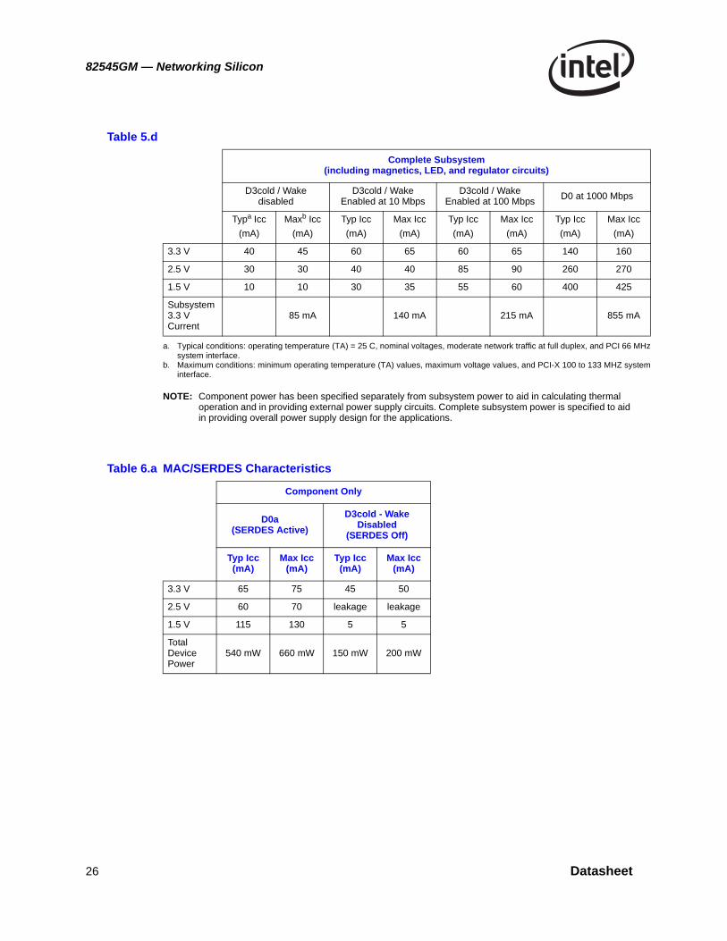
z
m
NOTE: Component power has been specified separately from subsystem power to aid in calculating thermal operation and in providing external power supply circuits. Complete subsystem power is specified to aid in providing overall power supply design for the applications.
Table 5.d
Complete Subsystem(including magnetics, LED, and regulator circuits)
D3cold / Wake disabled
D3cold / Wake Enabled at 10 Mbps
D3cold / Wake Enabled at 100 Mbps
D0 at 1000 Mbps
Typa Icc
(mA)
a. Typical conditions: operating temperature (TA) = 25 C, nominal voltages, moderate network traffic at full duplex, and PCI 66 MHsystem interface.
Maxb Icc
(mA)
b. Maximum conditions: minimum operating temperature (TA) values, maximum voltage values, and PCI-X 100 to 133 MHZ systeinterface.
Typ Icc
(mA)
Max Icc
(mA)
Typ Icc
(mA)
Max Icc
(mA)
Typ Icc
(mA)
Max Icc
(mA)
3.3 V 40 45 60 65 60 65 140 160
2.5 V 30 30 40 40 85 90 260 270
1.5 V 10 10 30 35 55 60 400 425
Subsystem 3.3 V Current
85 mA 140 mA 215 mA 855 mA
Table 6.a MAC/SERDES Characteristics
Component Only
D0a(SERDES Active)
D3cold - Wake Disabled
(SERDES Off)
Typ Icc(mA)
Max Icc(mA)
Typ Icc(mA)
Max Icc(mA)
3.3 V 65 75 45 50
2.5 V 60 70 leakage leakage
1.5 V 115 130 5 5
Total Device Power
540 mW 660 mW 150 mW 200 mW
26 Datasheet
Networking Silicon — 82545GM
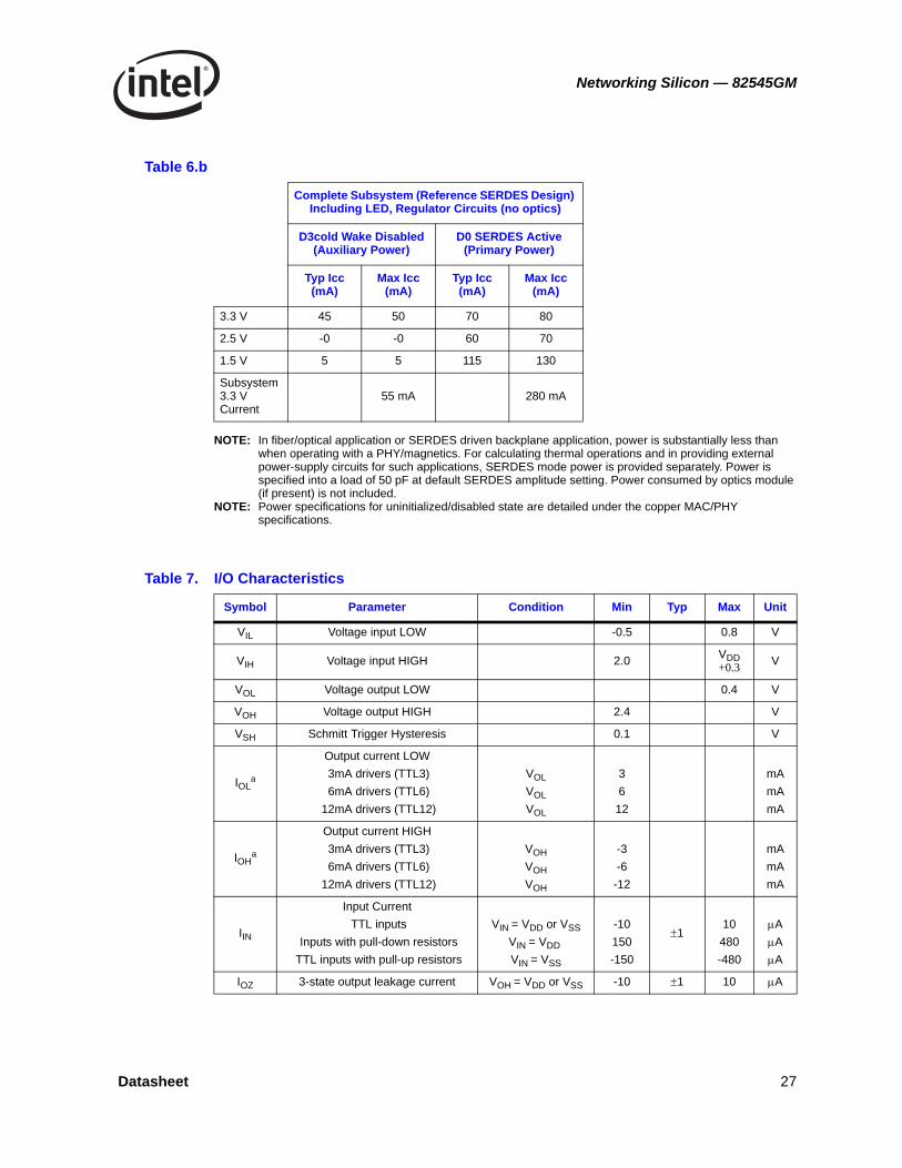
NOTE: In fiber/optical application or SERDES driven backplane application, power is substantially less than when operating with a PHY/magnetics. For calculating thermal operations and in providing external power-supply circuits for such applications, SERDES mode power is provided separately. Power is specified into a load of 50 pF at default SERDES amplitude setting. Power consumed by optics module (if present) is not included.
NOTE: Power specifications for uninitialized/disabled state are detailed under the copper MAC/PHY specifications.
Table 6.b
Complete Subsystem (Reference SERDES Design) Including LED, Regulator Circuits (no optics)
D3cold Wake Disabled (Auxiliary Power)
D0 SERDES Active (Primary Power)
Typ Icc(mA)
Max Icc(mA)
Typ Icc(mA)
Max Icc(mA)
3.3 V 45 50 70 80
2.5 V -0 -0 60 70
1.5 V 5 5 115 130
Subsystem 3.3 V Current
55 mA 280 mA
Table 7. I/O Characteristics
Symbol Parameter Condition Min Typ Max Unit
VIL Voltage input LOW -0.5 0.8 V
VIH Voltage input HIGH 2.0VDD+0.3
V
VOL Voltage output LOW 0.4 V
VOH Voltage output HIGH 2.4 V
VSH Schmitt Trigger Hysteresis 0.1 V
IOLa
Output current LOW
3mA drivers (TTL3)
6mA drivers (TTL6)
12mA drivers (TTL12)
VOL
VOL
VOL
3
6
12
mA
mA
mA
IOHa
Output current HIGH
3mA drivers (TTL3)
6mA drivers (TTL6)
12mA drivers (TTL12)
VOH
VOH
VOH
-3
-6
-12
mA
mA
mA
IIN
Input Current
TTL inputs
Inputs with pull-down resistors
TTL inputs with pull-up resistors
VIN = VDD or VSS
VIN = VDD
VIN = VSS
-10
150
-150
110
480
-480
A
A
A
IOZ 3-state output leakage current VOH = VDD or VSS -10 1 10 A
Datasheet 27

82545GM — Networking Silicon
5.4 AC Characteristics
CIN Input capacitanceAny input and bi-directional buffer
2.5 pF
COUT Output capacitance Any output buffer 2.0 pF
CPUD Pull-up/down Resistor value 7.5 20 k
a. TTL3 signals include: EE_DI, EE_SK, EE_CS, and JTAG_TDO.TTL6 signals include: FL_CE#, CLK_VIEW, FL_DATA[7:0], FL_ADDR[18:0], FL_OE#, and FL_WE#.TTL12 signals include: LED0 / LINK #, LED1 / ACT #, LED2 / LINK100 #, LED3 / LINK1000 #, SDP0, SDP1, SDP6, and SDP7.
Table 8. AC Characteristics: 3.3 V Interfacing
Symbol Parameter Min Typ Max Unit
fPCICLK Clock frequency in PCI mode 66 MHz
fPCICLK Clock frequency in PCI-X mode 66 133 MHz
Table 7. I/O Characteristics
Symbol Parameter Condition Min Typ Max Unit
Table 9. 25 MHz Clock Input Requirements
Symbol Parametera Min Typ Max Unit
fi_TX_CLK TX_CLK_IN frequency 25 - 50 ppm 2525 + 50
ppmMHz
a. This parameter applies to an oscillator connected to the Crystal One (XTAL1) input. Alternatively, a crystal may be connectedto XTAL1 and XTAL2 as the frequency source for the internal oscillator.
28 Datasheet

Networking Silicon — 82545GM
5.5 Serial Interface Specifications
Table 10. Link Interface Clock Requirements
Symbol Parameter Min Typ Max Unit
fGTXa
a. GTX_CLK is used externally for test purposes only.
GTX_CLK frequency 125 MHz
Table 11. EEPROM Interface Clock Requirements
Symbol Parameter Min Typ Max Unit
fSK 1 MHz
Table 12. AC Test Loads for General Output Pins
Symbol Signal Name Value Units
CL TDO 10 pF
CL APM_WAKEUP, PME#, SDP[7:6], SDP[1:0] 16 pF
CLEE_DI, EE_SK, FL_ADDR[18:0], FL_CS#, FL_OE#, FL_WE#, FL_DATA[7:0]
18 pF
CL RX_ACTIVITY, TX_ACTIVITY, LINK_UP 20 pF
Figure 3. AC Test Loads for General Output Pins
Table 13. Driver Characteristics
Symbol Parameter Min Typ Max Units
VOD Differential Output Voltage Swinga 875 1325
mVpeak-peak
VOS Output Offset Voltage 1075 1325 mV
Delta VOD Change in VOD between 0 and 1b 25 mV
CL
Datasheet 29

82545GM — Networking Silicon
5.6 Timing Specifications
Note: Timing specifications are preliminary and subject to change. Verify with your local Intel sales office that you have the latest information before finalizing a design.
5.6.1 PCI/PCI-X Bus Interface
5.6.1.1 PCI/PCI-X Bus Interface Clock
RO Differential Output Impedance
80 120
ISA, ISB Output Current on Short to VSS
40 mA
ISABOutput Current when A and B are Shorted
12 mA
a. This is the maximum inside dimension of the eye pattern, measured on high and low data pat-terns with pre-emphasis present. Load - 100 .
b. This is defined as an absolute value of amplitude jitter.
Table 14. Receiver Characteristics
Symbol Parameter Min Typ Max Units
VID Differential Input Voltage Swing
100 2000mV
peak-peak
RIN Differential Input Impedance
80 120
Table 15. PCI/PCI-X Bus Interface Clock Parameters
Symbol Parametera
a. Rise and fall times are specified in terms of the edge rate measured in V/ns. This slew rate must be met across the minimumpeak-to-peak portion of the clock waveform as shown.
PCI-X 133 MHz
PCI-X 66 MHz PCI 66MHz PCI 33 MHzUnits
Min Max Min Max Min Max Min Max
TCYC CLK cycle time 7.5 20 15 20 15 30 30 ns
TH CLK high time 3 6 6 11 ns
TL CLK low time 3 6 6 11 ns
CLK slew rate 1.5 4 1.5 4 1.5 4 1 4 V/ns
RST# slew rateb
b. The minimum RST# slew rate applies only to the rising (de-assertion) edge of the reset signal and ensures that system noisecannot render a monotonic signal to appear bouncing in the switching range.
50 50 50 50 mV/ns
Table 13. Driver Characteristics
Symbol Parameter Min Typ Max Units
30 Datasheet

Networking Silicon — 82545GM
5.6.1.2 PCI/PCI-X Bus Interface Timing
NOTES:1. Output timing measurements are as shown.2. REQ# and GNT# signals are point-to-point and have different output valid delay and input setup times than
bussed signals. GNT# has a setup of 10 ns; REQ# has a setup of 12 ns. All other signals are bussed.3. Input timing measurements are as shown.
Figure 4. PCI/PCI-X Clock Timing
Table 16. PCI/PCI-X Bus Interface Timing Parameters
Symbol Parameter
PCI-X 133 MHz
PCI-X 66 MHz PCI 66MHz PCI 33 MHzUnits
Min Max Min Max Min Max Min Max
TVALCLK to signal valid delay: bussed signals
0.7 3.8 0.7 3.8 2 6 2 11 ns
TVAL(ptp)
CLK to signal valid delay: point-to-point signals
0.7 3.8 0.7 3.8 2 6 2 12 ns
TON Float to active delay 0 0 2 2 ns
TOFF Active to float delay 7 7 14 28 ns
TSUInput setup time to CLK: bussed signals
1.2 1.7 3 7 ns
TSU(ptp)
Input setup time to CLK: point-to-point signals
1.2 1.7 510, 12
ns
TH Input hold time from CLK 0.5 0.5 0 0 ns
TRRSUREQ64# to RST# setup time
10*TCYC
10*TCYC
10*TCYC
10*TCYC
ns
TRRHRST# to REQ64# hold time
0 0 0 0 ns
0.6 Vcc
0.2 Vcc
0.5 Vcc
0.4 Vcc
0.3 Vcc
Tcyc
Th
Tl
0.4 Vcc p-to-p(minimum)
3.3 V Clock
Datasheet 31

82545GM — Networking Silicon
Figure 5. PCI Bus Interface Output Timing Measurement
VTH
VTL
VTESTPCI_CLK
VTEST
VSTEP (3.3V Signalling)OutputDelay
Tri-StateOutput
output current leakage current
TON
TOFF
Figure 6. PCI Bus Interface Input Timing Measurement Conditions
VTH
VTL
VTESTPCI_CLK
TSU
VTESTInput VMAXVTEST
VTL
VTH
InputValid
TH
Table 13. PCI Bus Interface Timing Measurement Conditions
Symbol Parameter PCI-XPCI 66 MHz
3.3 vUnit
VTH Input measurement test voltage (high) 0.6*VCC 0.6*VCC V
VTL Input measurement test voltage (low) 0.25*VCC 0.2*VCC V
VTEST Output measurement test voltage 0.4*VCC 0.4*VCC V
Input signal slew rate 1.5 1.5 V/ns
32 Datasheet

Networking Silicon — 82545GM
5.6.2 Link Interface Timing
5.6.2.1 Link Interface Rise and Fall Time
Figure 7. TVAL (max) Rising Edge Test Load
10 pF25Ω
Pin TestPoint1/2 inch max.
Figure 8. TVAL (max) Falling Edge Test Load
Table 17. Rise and Fall Times
Symbol Parameter Condition Min Max Unit
TR Clock rise time 0.8 V to 2.0 V 0.7 ns
TF Clock fall time 2.0 V to 0.8 V 0.7 ns
TR Data rise time 0.8 to 2.0 V 0.7 ns
TF Data fall time 2.0 V to 0.8 V 0.7 ns
10 pF25Ω
Pin TestPoint1/2 inch max.
VCC
Datasheet 33

82545GM — Networking Silicon
5.6.2.2 Link Interface Transmit Timing
Figure 9. Link Interface Rise/Fall Timing
Figure 10. Transmit Interface Timing
2.0 V
0.8 V
TFTR
1.4VTX_CLOCK
TSU
TX_DATA[9:0] Valid Data
TH
TPERIOD
Table 18. Transmit Interface Timing
Symbol Parameter Min Typ Max Unit
TPERIODGTX_CLK perioda
TBI mode (1000 Mbps)8 ns
TSETUP Data setup to rising GTX_CLK 2.5 ns
THOLD Data hold from rising GRX_CLK 1.0 ns
TDUTY GTX_CLK duty cycle 40 60 %
a. GTX_CLK should have a 100 ppm tolerance.
34 Datasheet

Networking Silicon — 82545GM
5.6.2.3 Link Interface Receive Timing
Figure 11. Receive Interface Timing
1.4VRBC1
TSU
RX_DATA[9:0]COMMA
Code_Group
TH
COM_DET
ValidData
0.8V
2.0V
RBC01.4V
THTSUTA-B
0.8V
2.0V
Table 19. Transmit Interface Timing
Symbol Parameter Min Typ Max Unit
TREQRBC0/RBC1 frequencyTBI mode (1000 Mbps)
62.5 MHz
TSETUP Data setup before rising RBC0/RBC1 2.5 ns
THOLD Data hold after rising RBC0/RBC1 1 ns
TDUTY RBC0/RBC1 duty cycle 40 60 %
TA-B RBC0/RBC1 skew 7.5 8.5 ns
Datasheet 35

82545GM — Networking Silicon
5.6.3 Flash Interface
Figure 12. Flash Read Timing
0ns 250ns
Flash CE#
Flash OE#
Flash WE#
Flash Address [18:0]
Flash Data
Table 20. Flash Read Operation Timing
Symbol Parameter Min Typ Max Unit
TCE Flash CE# or OE# to read data delay 160 ns
TACC Flash address setup time 160 ns
THOLD Data hold time 0 ns
Figure 13. Flash Write Timing
0ns 250ns 500ns
Flash CE#
Flash OE#
Flash WE#
Flash Address [18:0]
Flash Data
36 Datasheet

Networking Silicon — 82545GM
5.6.4 EEPROM Interface
Table 21. Flash Write Operation Timing
Symbol Parameter Min Typ Max Unit
TWE Flash write pulse width (WE#) 160 ns
TAH Flash address hold time 0 ns
TDS Flash data setup time 160 ns
Table 22. Link Interface Clock Requirements
Symbol Parameter Min Typ Max Unit
TPW EE_SK pulse width TPERIOD*128 ns
Table 23. Link Interface Clock Requirements
Symbol Parametera Min Typ Max Unit
TDOS EE_DO setup time TCYC*2 ns
TDOH EE_DO hold time 0 ns
a. The EE_DO setup and hold time is a function of the CLK cycle time but is referenced to O_EE_SK.
Datasheet 37

82545GM — Networking Silicon
Note: This page left intentionally blank.
38 Datasheet

Networking Silicon — 82545GM
6.0 Package and Pinout Information
6.1 Device Identification
NOTE: The dot in the lower left corner indicates the location of pin 1.
Figure 14. 82545GM Device Identification Markings
RC82545GM S Unnn
Country
YYWW
Fnnnnnnnn
Intel'ZZ
®
RC82545GM Product Name
YYWW Date Code
Fnnnnnnnn Lot Trace Code
(c)’ZZ Copyright Information
Country Country of Origin Assembly
Datasheet 39

82545GM — Networking Silicon
6.2 Lead-Free Device Identification
Figure 15. Lead-Free 82545GM Device Identification Markings
int Rel
Pin 1 Indicator
PC82545GM
Q542 SAMPLEYYWW Xnnnnnnnn
TAIWAN
‘03C e1
PC82545GM Product Name
YYWW Date Code
Xnnnnnnnn Lot Trace Code
(c)’03 (e1)Copyright Information and Lead-Free Mark
Taiwan Country of Origin Assembly
40 Datasheet

Networking Silicon — 82545GM
6.3 Package Information
The 82545GM device is a 364-lead ball grid array (BGA) measuring 21 mm2. The package dimensions are detailed in the figures below. The nominal ball pitch is 1 mm.
Figure 16. 82545GM 364-Lead BGA Ball Pad Dimensions
0.40 +/- 0.05 mm Solder Mask Opening
Detail Area
0.55 +/- 0.05 mm Pad Size
Datasheet 41

82545GM — Networking Silicon
Figure 17. 82545GM Mechanical Specifications
1.00
21.0
0±0.1
0
SE
AT
ING
PL
AN
E
(0.36)
-C-
0.25 C
1.70 MAX
0.30~0.50
0.20
0.2
0(4
X)
-A-
P YWVUTRK M NLJHGF
P
-B-
1.0
0
YWVUTR
21.00±0.10
19.00
M NLKJHGF
A C EDB
15
43
28
76
PIN
1 C
OR
NE
R
BO
TT
OM
VIE
WT
OP
VIE
W
10
12
11
10
91
41
31
51
91
81
61
72
01
71
81
92
01
11
31
61
51
41
2
A C EDB
34
56
78
91
2
PIN
1 C
OR
NE
R
42 Datasheet

Networking Silicon — 82545GM
6.4 Thermal Specifications
The 82545GM device is specified for operation when the ambient temperature (TA) is within the range of 0° C (minimum ambient temperature) to 70° C (maximum ambient temperature). The maximum junction temperature for the device is 120° C.
TC (case temperature) is calculated using the equation:
TC = TA + P (JA - JC)
TJ (junction temperature) is calculated using the equation:
TJ = TA + P JA
P (power consumption) is calculated by using the typical ICC and nominal VCC. The thermal resistances are shown in Table 24.
Thermal resistances are determined empirically with test devices mounted on standard thermal test boards. Real system designs may have different characteristics due to board thickness, arrangement of ground planes, and proximity of other components. The case temperature measurements should be used to assure that the 82545GM device is operating under recommended conditions.
Table 24. Thermal Characteristics
Symbol ParameterValue at specified airflow (m/s)
Units0 1 2
JA Thermal resistance, junction-to-ambient 19.2 17.1 15.4 C/Watt
JC Thermal resistance, junction-to-case 4.6 4.6 4.6 C/Watt
Datasheet 43

82545GM — Networking Silicon
6.5 Ball Mapping Diagram
Note: The 82545GM device uses five categories of VDD connections: VDDO (3.3 V), AVDDH (Analog 3.3 V), AVDDL (Analog 2.5 V), and DVDD (1.5 V).
6.6 Pinout Information
Table 25. PCI Address, Data, and Control Signals
Signal Pin Signal Pin Signal Pin
PCI_AD[0] T14 PCI_AD[28] Y3 PCI_AD[56} T17
PCI_AD[1] V14 PCI_AD[29] U4 PCI_AD[57] U18
PCI_AD[2] Y15 PCI_AD[30] V3 PCI_AD[58] V18
1 2 3 4 5 6 7 8 9 10 11 12 13 14 15 16 17 18 19 20
A
B
C
D
E
F
G
H
J
K
L
M
N
P
R
T
U
V
W
Y
44 Datasheet

Networking Silicon — 82545GM
PCI_AD[3] W14 PCI_AD[31] V1 PCI_AD[59] U16
PCI_AD[4] T13 PCI_AD[32] L16 PCI_AD[60] V17
PCI_AD[5] V13 PCI_AD[33] M20 PCI_AD[61] W18
PCI_AD[6] Y14 PCI_AD[34] M19 PCI_AD[62] Y19
PCI_AD[7] U12 PCI_AD[35] M16 PCI_AD[63] T16
PCI_AD[8] V12 PCI_AD[36] M18 CBE[0]# Y13
PCI_AD[9] T12 PCI_AD[37] M17 CBE[1]# V10
PCI_AD[10] W12 PCI_AD[38] N20 CBE[2]# T8
PCI_AD[11] Y12 PCI_AD[39] N16 CBE[3]# Y4
PCI_AD[12] V11 PCI_AD[40] P20 CBE[4]# V16
PCI_AD[13] T11 PCI_AD[41] N18 CBE[5]# Y18
PCI_AD[14] Y11 PCI_AD[42] P19 CBE[6]# Y17
PCI_AD[15] W10 PCI_AD[43] P16 CBE[7]# T15
PCI_AD[16] U8 PCI_AD[44] R20 PAR U10
PCI_AD[17] Y7 PCI_AD[45] P18 PAR64 V15
PCI_AD[18] Y6 PCI_AD[46] P17 FRAME# V8
PCI_AD[19] V7 PCI_AD[47] T20 IRDY# W8
PCI_AD[20] T7 PCI_AD[48] R16 TRDY# Y8
PCI_AD[21] W6 PCI_AD[49] U20 STOP# V9
PCI_AD[22] Y5 PCI_AD[50] R18 IDSEL T6
PCI_AD[23] V6 PCI_AD[51] T19 DEVSEL# T9
PCI_AD[24] U6 PCI_AD[52] V20 VIO Y1
PCI_AD[25] V5 PCI_AD[53] T18 VIO Y20
PCI_AD[26] W4 PCI_AD[54] W20
PCI_AD[27] V4 PCI_AD[55] V19
Table 26. PCI Arbitration Signals
Signal Pin Signal Pin Signal Pin
REQ64# U14 REQ# W2 LOCK# Y9
ACK64# W16 GNT# T3
Table 27. Interrupt Signals
Signal Pin Signal Pin Signal Pin
INTA# Y2
Table 25. PCI Address, Data, and Control Signals
Signal Pin Signal Pin Signal Pin
Datasheet 45

82545GM — Networking Silicon
Table 28. System Signals
Signal Pin Signal Pin Signal Pin
CLK U2 M66EN Y16 RST# T5
Table 29. Error Reporting Signals
Signal Pin Signal Pin Signal Pin
SERR# T10 PERR# Y10
Table 30. Power Management Signals
Signal Pin Signal Pin Signal Pin
LAN_PWR_GOOD
A17 PME# T4 AUX_PWR R3
Table 31. Impedance Compensation Signals
Signal Pin Signal Pin Signal Pin
ZN_COMP T2 ZP_COMP R5
Table 32. SMB Signals
Signal Pin Signal Pin Signal Pin
SMBCLK A14 SMBDATA A15 SMBALRT# A16
Table 33. EEPROM Interface Signals
Signal Pin Signal Pin Signal Pin
EE_DI C19 EE_CS C20 EE_SK D20
EE_DO B20
Table 34. Flash Interface Signals
Signal Pin Signal Pin Signal Pin
FL_ADDR[0] F16 FL_ADDR[10] G17 FL_OE# K18
FL_ADDR[1] E18 FL_ADDR[11] G16 FL_WE# C17
FL_ADDR[2] E16 FL_ADDR[12] B15FL_DATA[0]/LAN_DISABLE
H16
FL_ADDR[3] E15 FL_ADDR[13] D19 FL_DATA[1] G18
FL_ADDR[4] E14 FL_ADDR[14] D18 FL_DATA[2] J16
FL_ADDR[5] E13 FL_ADDR[15] C15 FL_DATA[3] H18
FL_ADDR[6] D15 FL_ADDR[16] D16 FL_DATA[4] J17
46 Datasheet

Networking Silicon — 82545GM
FL_ADDR[7] B16 FL_ADDR[17] C18 FL_DATA[5] J18
FL_ADDR[8] F17 FL_ADDR[18] D17 FL_DATA[6] K17
FL_ADDR[9] F18 FL_CS# H20 FL_DATA[7] K16
Table 34. Flash Interface Signals
Signal Pin Signal Pin Signal Pin
Table 35. LED Signals
Signal Pin Signal Pin Signal Pin
ACT# N1 LINK100# N4 LINK1000# N3
LINK# M1
Table 36. Software Definable Signals
Signal Pin Signal Pin Signal Pin
SDP[0] G4 SDP[6] E12 SDP[7] E11
SDP[1] G5
Table 37. PHY Signals
Signal Pin Signal Pin Signal Pin
XTAL1 A3 MDI0+ B2 MDI2+ D2
XTAL2 A4 MDI1- C1 MDI3- E1
REF E3 MDI1+ C2 MDI3+ E2
MDI0- B1 MDI2- D1
Table 38. Serializer/Deserializer (SERDES) Signals
Signal Pin Signal Pin Signal Pin
RX+ G19 TX+ F19 SIG_DETECT E20
RX- G20 TX- F20
Table 39. Test Interface Signals
Signal Pin Signal Pin Signal Pin
JTAG_TCK P1 JTAG_TMS P5 CLK_VIEW P3
JTAG_TDI P4 JTAG_RST# N5 TEST# A8
JTAG_TDO P2
Datasheet 47

82545GM — Networking Silicon
Table 40. Power Support Signals
Signal Pin Signal Pin Signal Pin
CTRL_15 A18 CTRL_25 F2
Table 41. Digital Power Signals
Signal Pin Signal Pin Signal Pin
VDDO (3.3V) B8 VDDO (3.3V) U7 DVDD (1.5V) H13
VDDO (3.3V) B14 VDDO (3.3V) U11 DVDD (1.5V) H14
VDDO (3.3V) B19 VDDO (3.3V) U15 DVDD (1.5V) J7
VDDO (3.3V) C10 VDDO (3.3V) U19 DVDD (1.5V) J14
VDDO (3.3V) C16 VDDO (3.3V) W1 DVDD (1.5V) M7
VDDO (3.3V) D6 VDDO (3.3V) W5 DVDD (1.5V) M14
VDDO (3.3V) D11 VDDO (3.3V) W9 DVDD (1.5V) N7
VDDO (3.3V) E17 VDDO (3.3V) W13 DVDD (1.5V) N8
VDDO (3.3V) H4 VDDO (3.3V) W17 DVDD (1.5V) N13
VDDO (3.3V) H19 DVDD (1.5V) G7 DVDD (1.5V) N14
VDDO (3.3V) L17 DVDD (1.5V) G8 DVDD (1.5V) P7
VDDO (3.3V) M2 DVDD (1.5V) G9 DVDD (1.5V) P8
VDDO (3.3V) N19 DVDD (1.5V) G12 DVDD (1.5V) P9
VDDO (3.3V) R4 DVDD (1.5V) G13 DVDD (1.5V) P12
VDDO (3.3V) R17 DVDD (1.5V) G14 DVDD (1.5V) P13
VDDO (3.3V) U1 DVDD (1.5V) H7 DVDD (1.5V) P14
VDDO (3.3V) U3 DVDD (1.5V) H8
Table 42. Analog Power Signals
Signal Pin Signal Pin Signal Pin
AVDDH (3.3 V) B4 AVDDL (2.5 V) G1 AVDDL (2.5 V) L2
AVDDH (3.3 V) F1 AVDDL (2.5 V) G2 AVDDL (2.5 V) L5
AVDDL (2.5 V) A19 AVDDL (2.5 V) G3 AVDDL (2.5 V) L18
Table 43. Grounds and No Connect Signals
Signal Pin Signal Pin Signal Pin
GND A1 GND K12 NC A13
GND A2 GND K13 NC B12
GND A5 GND K14 NC B13
GND A10 GND L7 NC C12
GND B3 GND L8 GND W15
48 Datasheet

Networking Silicon — 82545GM
GND B6 GND L9 GND W19
GND B11 GND L10 NC A11
GND B17 GND L11 NC A12
GND C3 GND L12 NC C13
GND D3 GND L13 NC C14
GND D8 GND L14 NC D12
GND D14 GND L19 NC D13
GND E19 GND M4 NC F4
GND F3 GND M8 NC F5
GND G10 GND M9 NC H1
GND G11 GND M10 NC H3
GND H2 GND M11 NC H5
GND H9 GND M12 NC J1
GND H10 GND M13 NC J2
GND H11 GND N9 NC J3
GND H12 GND N10 NC J4
GND H17 GND N11 NC J5
GND J8 GND N12 NC J19
GND J9 GND N17 NC J20
GND J10 GND P10 NC K1
GND J11 GND P11 NC K3
GND J12 GND R2 NC K19
GND J13 GND R19 NC K20
GND K2 GND U5 NC L1
GND K4 GND U9 NC L3
GND K5 GND U13 NC L4
GND K7 GND U17 NC M3
GND K8 GND V2 NC N2
GND K9 GND W3 NC T1
GND K10 GND W7
GND K11 GND W11
Table 44. Reserved Signals
Signal Pin Signal Pin Signal Pin
Reserved[0] D4 Reserved[11] B7 Reserved[22] B10
Reserved[1] D5 Reserved[12] A7 Reserved[23] C6
Reserved[2] C4 Reserved[13] C8 Reserved[24] A20
Table 43. Grounds and No Connect Signals
Signal Pin Signal Pin Signal Pin
Datasheet 49

82545GM — Networking Silicon
Reserved[3] E4 Reserved[14] E8 Reserved[25] B18
Reserved[4] C5 Reserved[15] E9 Reserved[26] M5
Reserved[5] E5 Reserved[16] D9 Reserved[27] E7
Reserved[6] B5 Reserved[17] C9 Reserved[28] A6
Reserved[7] E6 Reserved[18] B9 Reserved[29] R1
Reserved[8] D7 Reserved[19] D10 Reserved[30] L20
Reserved[9] C7 Reserved[20] A9
Reserved[10] E10 Reserved[21] C11
Table 44. Reserved Signals
Signal Pin Signal Pin Signal Pin
50 Datasheet