Embed Size (px)
Citation preview
04/19/23NASA Workmanship Standards1
José D. Sancho
ESD Class 0 ProtectionESD Class 0 Protection Stress Levels Stress Levels
Their Origin and ApplicationTheir Origin and Application
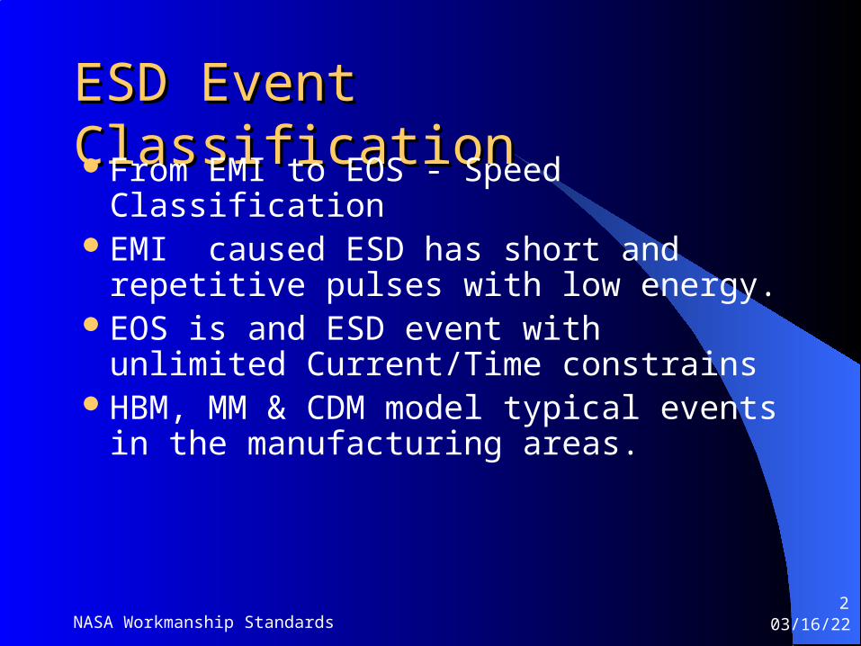
ESD Event ClassificationESD Event ClassificationFrom EMI to EOS - Speed ClassificationEMI caused ESD has short and repetitive
pulses with low energy.EOS is and ESD event with unlimited
Current/Time constrainsHBM, MM & CDM model typical events
in the manufacturing areas.
04/19/23NASA Workmanship Standards2
04/19/23NASA Workmanship Standards3
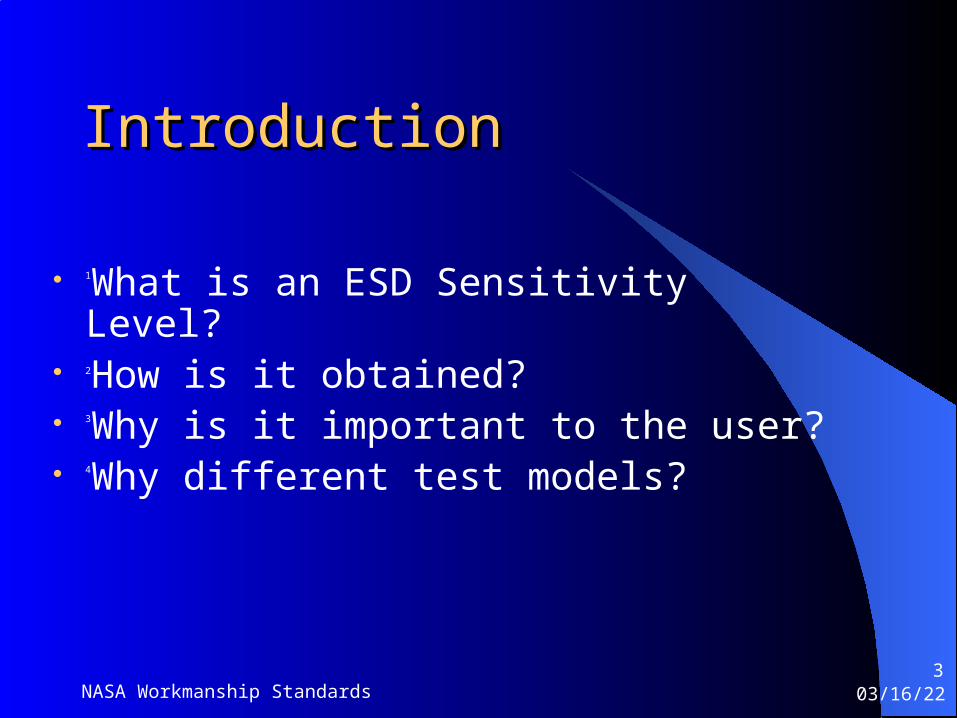
Introduction Introduction
1What is an ESD Sensitivity Level? 2How is it obtained? 3Why is it important to the user? 4Why different test models?
04/19/23NASA Workmanship Standards4
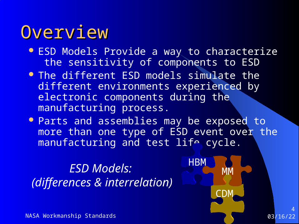
Overview Overview ESD Models Provide a way to characterize the
sensitivity of components to ESD The different ESD models simulate the different
environments experienced by electronic components during the manufacturing process.
Parts and assemblies may be exposed to more than one type of ESD event over the manufacturing and test life cycle.
CDM
MM
HBMESD Models:
(differences & interrelation)
04/19/23NASA Workmanship Standards5
Purpose of ESD Models Purpose of ESD Models
Models establish Benchmarks for ESD Sensitivity.
Different Models are used to simulate different work environments.
Models provide help to prevent and analyze ESD Failures
04/19/23NASA Workmanship Standards6
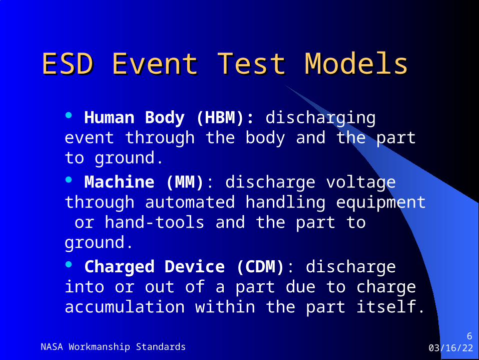
Human Body (HBM): discharging event through the body and the part to ground. Machine (MM): discharge voltage through automated handling equipment or hand-tools and the part to ground. Charged Device (CDM): discharge into or out of a part due to charge accumulation within the part itself.
ESD Event Test ModelsESD Event Test Models
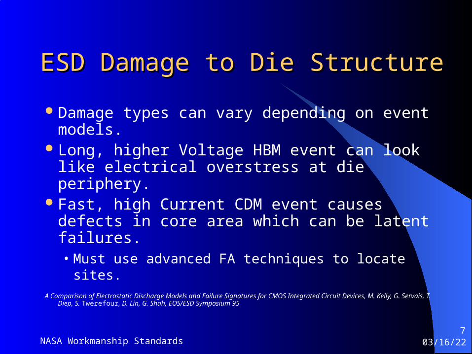
ESD Damage to Die StructureESD Damage to Die Structure
Damage types can vary depending on event models.
Long, higher Voltage HBM event can look like electrical overstress at die periphery.
Fast, high Current CDM event causes defects in core area which can be latent failures.• Must use advanced FA techniques to locate sites.
A Comparison of Electrostatic Discharge Models and Failure Signatures for CMOS Integrated Circuit Devices, M. Kelly, G. Servais, T. Diep, S. Twerefour, D. Lin, G. Shah, EOS/ESD Symposium 95
04/19/23NASA Workmanship Standards7

ESD Sensitivity LevelsESD Sensitivity Levels
Human Body Model Machine Model Charged Device Model
Class 0 <250 V Class M1 < 100 V Class C1 < 125 V
Class 1A 250 V to< 500 V Class M2 100 V to < 200 V Class C2 125 V to < 250 V
Class 1B 500 V to < 1 kV Class M3 200 V to < 400 V Class C3 250 V to < 500 V
Class 1C 1 kV to < 2 kV Class M4 ≥ 400 V Class C4 500 V to <1 kV
Class 2 2 kV to < 4 kV --- --- Class C5 1 kV to < 1.5 kV
Class 3A 4 kV to < 8 kV --- --- Class C6 1.5 kV to < 2 kV
Class 3B ≥ 8 kV --- --- Class C7 ≥ 2 kV
04/19/23NASA Workmanship Standards8

04/19/23NASA Workmanship Standards9
White Paper 2: A Case for Lowering Component Level CDM ESD Specifications and Requirements, Industry Council on ESD Target Levels, March 2009
04/19/23NASA Workmanship Standards10
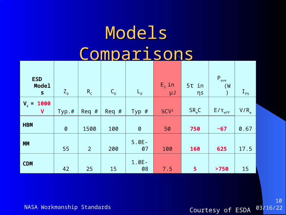
Models ComparisonsModels Comparisons
ESD Models ZD RC CD LD ΕS in μJ 5τ in ηs Pave (W) IPS
Vc = 1000 V Typ.# Req # Req # Typ # ½CV2 5ReC Ε/τeff V/Re
HBM0 1500 100 0 50 750 ~67 0.67
MM55 2 200 5.0E-07 100 160 625 17.5
CDM42 25 15 1.0E-08 7.5 5 >750 15
Courtesy of ESDA
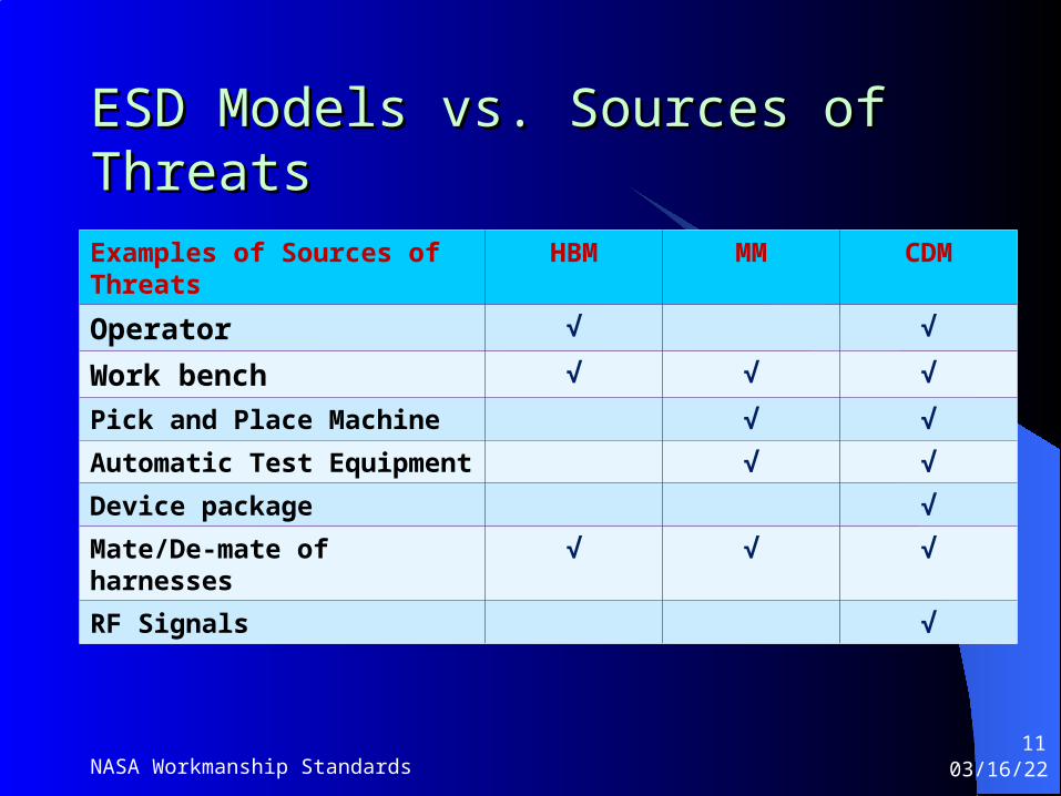
ESD Models vs. Sources of ThreatsESD Models vs. Sources of Threats
Examples of Sources of Threats HBM MM CDM
Operator √ √
Work bench √ √ √
Pick and Place Machine √ √
Automatic Test Equipment √ √
Device package √
Mate/De-mate of harnesses √ √ √
RF Signals √
04/19/23NASA Workmanship Standards11

““Class 0” Parts ProtectionClass 0” Parts Protection
“Class 0” has become the generic term to define parts which are very sensitive to ESD.
It now encompass parts sensitive to HBM <250v as well as parts damaged by EMI
Sensitivity for these parts needs to be also defined using CDM classifications.
{EPAs as currently implemented at GSFC can protect parts sensitive to ~100 V HBM}
04/19/23NASA Workmanship Standards12
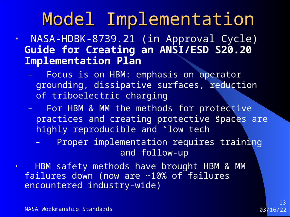
Model ImplementationModel Implementation• NASA-HDBK-8739.21 (in Approval Cycle) Guide
for Creating an ANSI/ESD S20.20 Implementation Plan– Focus is on HBM: emphasis on operator grounding,
dissipative surfaces, reduction of triboelectric charging
– For HBM & MM the methods for protective practices and creating protective spaces are highly reproducible and “low tech”
– Proper implementation requires training and follow-up
• HBM safety methods have brought HBM & MM failures down (now are ~10% of failures encountered industry-wide)
04/19/23NASA Workmanship Standards13
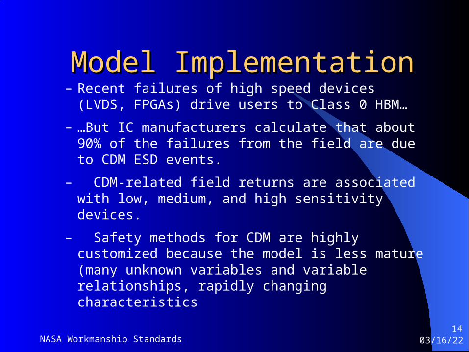
Model ImplementationModel Implementation– Recent failures of high speed devices (LVDS, FPGAs)
drive users to Class 0 HBM…
– …But IC manufacturers calculate that about 90% of the failures from the field are due to CDM ESD events.
– CDM-related field returns are associated with low, medium, and high sensitivity devices.
– Safety methods for CDM are highly customized because the model is less mature (many unknown variables and variable relationships, rapidly changing characteristics
04/19/23NASA Workmanship Standards14
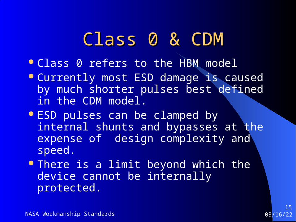
Class 0 & CDMClass 0 & CDMClass 0 refers to the HBM modelCurrently most ESD damage is caused by
much shorter pulses best defined in the CDM model.
ESD pulses can be clamped by internal shunts and bypasses at the expense of design complexity and speed.
There is a limit beyond which the device cannot be internally protected.
04/19/23NASA Workmanship Standards15

Limits of Design-in ProtectionLimits of Design-in Protection
CDM protection by the design is driven by the peak current from the IC package discharge at the CDM voltage targeted.
The larger the package the higher the peak current of the CDM pulse created.
The smaller the geometry of the circuit the lower the breakdown voltage of the circuit
Present Theoretical Limit ≈ 125v CDM
04/19/23NASA Workmanship Standards16

Protection of Devices Sensitive to Class 0 ESDProtection of Devices Sensitive to Class 0 ESD
• “Shalls” related to HBM Class 0 protection:• Dissipative chairs and stools
• Conductive or dissipative floors or floor mats
• Relative humidity
• Ionizers
• Smocks
• Procedures for Mating and de-mating of harnesses
• Soldering iron testing
• Signage
04/19/23NASA Workmanship Standards17
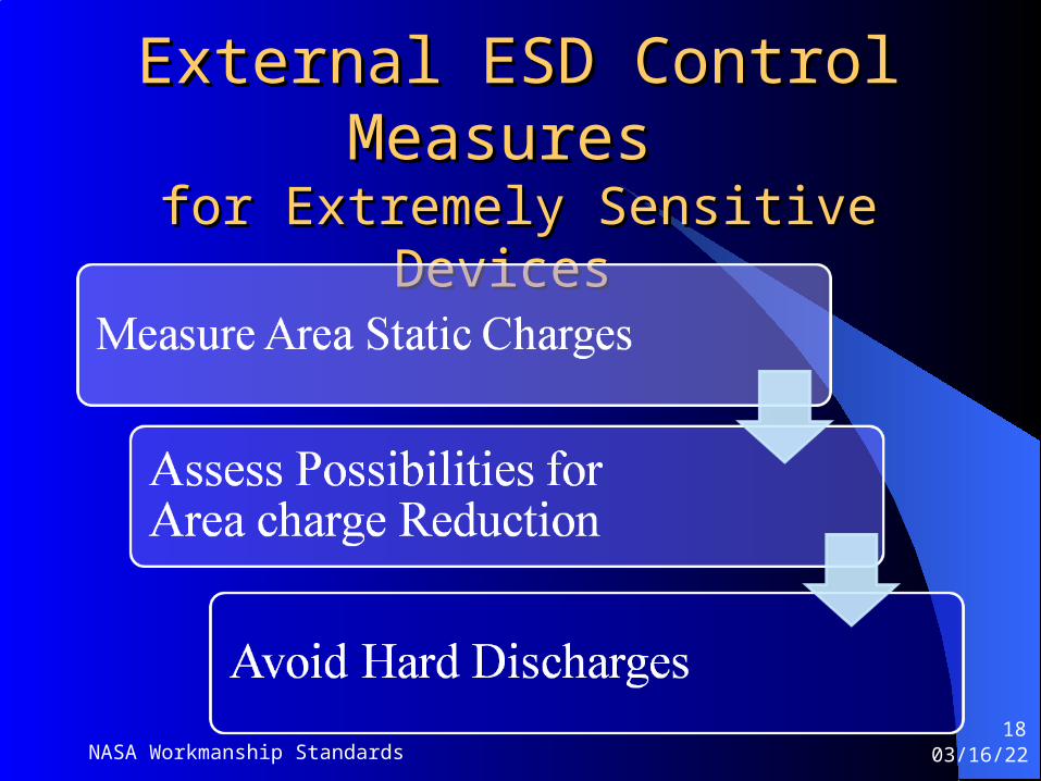
External ESD Control Measures External ESD Control Measures for Extremely Sensitive Devices for Extremely Sensitive Devices
04/19/23NASA Workmanship Standards18
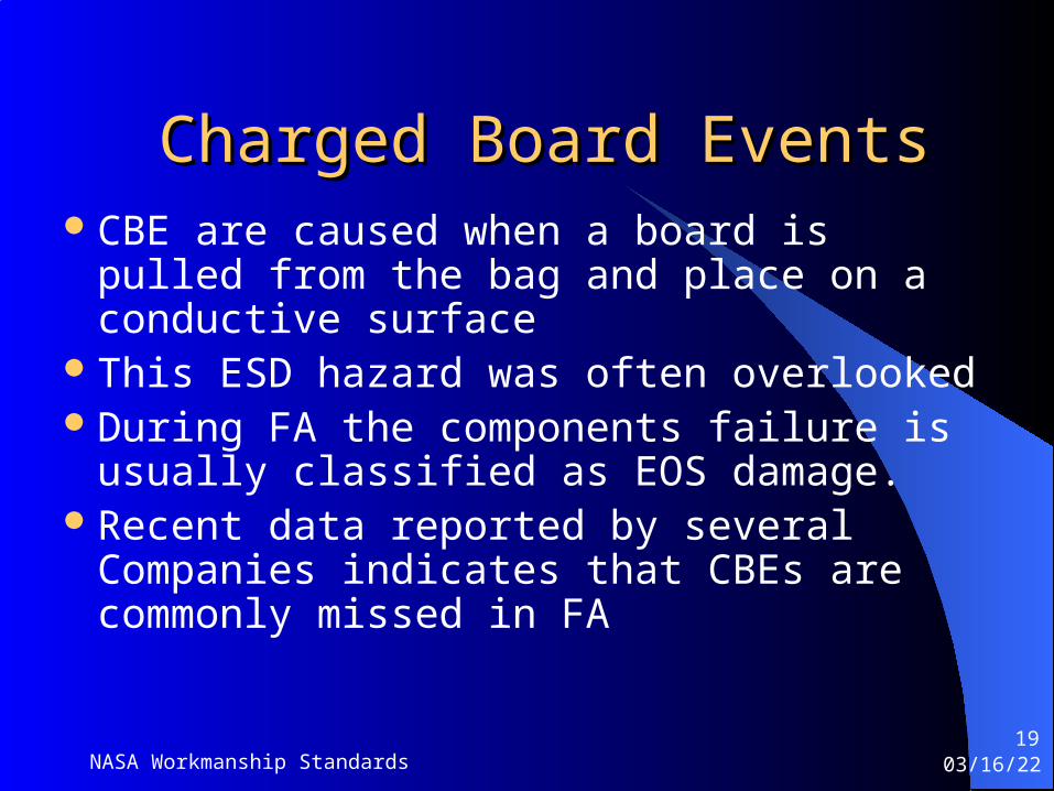
Charged Board EventsCharged Board EventsCBE are caused when a board is pulled from
the bag and place on a conductive surfaceThis ESD hazard was often overlookedDuring FA the components failure is usually
classified as EOS damage.Recent data reported by several Companies
indicates that CBEs are commonly missed in FA
04/19/23NASA Workmanship Standards19
04/19/23NASA Workmanship Standards20
Where to Get More InformationWhere to Get More Information
WEB searches under “ESD Models”ESDA publicationsConsulting services provide Advice on
tough ESD problems and Solutions.
04/19/23NASA Workmanship Standards21
ReferencesReferences1. ANSI/ESD STM5.1-2001 ESD Sensitivity Testing (HBM)2. ANSI/ESD STM5.2-1999 ESD Sensitivity Testing (MM)3. ANSI/ESD STM5.3.1-1999 ESD Sensitivity Testing (CDM)4. ANSI/ESD SP5.2.2-2004 ESD Sensitivity Testing (SDM)5. ANSI/ESD SP5.5.1-2004 ESD Sensitivity Testing (TPL)6. Scott M. Hull, “ESD Failures in Thin-Film Resistors”
NASA/Goddard Space Flight Center 7. http://esdsystems.com/whitepapers/8. http://www.semiconfareast.com9. http://www.ce-mag.com/archive/01/09/henry.html10. http://www.ce-mag.com/ce-mag.com/archive/01/03/0103CE_046.html11. White Paper: Industry Council on ESD Target Levels on CDM12. http://ossma-dev.gsfc.nasa.gov/ESDResources/index.php13. https://ossmacm.gsfc.nasa.gov/
Thank youThank youAny Questions?Any Questions?
04/19/23NASA Workmanship Standards22
04/19/23NASA Workmanship Standards23
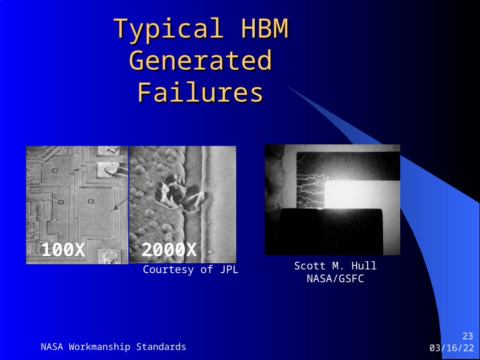
Typical HBM Typical HBM Generated FailuresGenerated Failures
2000X100XCourtesy of JPL Scott M. Hull NASA/GSFC
04/19/23NASA Workmanship Standards24
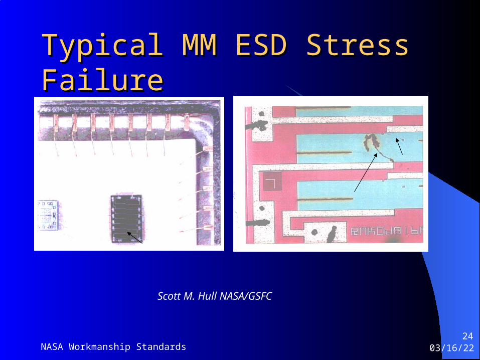
Typical MM ESD Stress FailureTypical MM ESD Stress Failure
Scott M. Hull NASA/GSFC
04/19/23NASA Workmanship Standards25
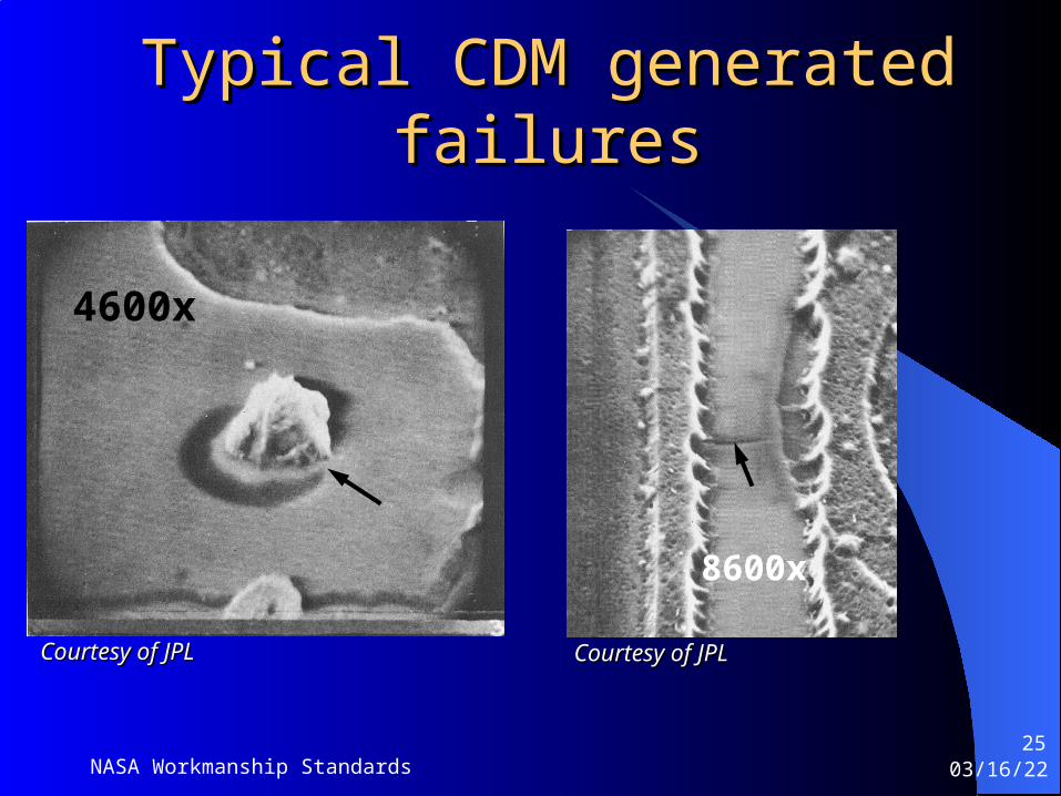
Typical CDM generated failuresTypical CDM generated failures
4600x
8600x
Courtesy of JPLCourtesy of JPLCourtesy of JPLCourtesy of JPL
04/19/23NASA Workmanship Standards26
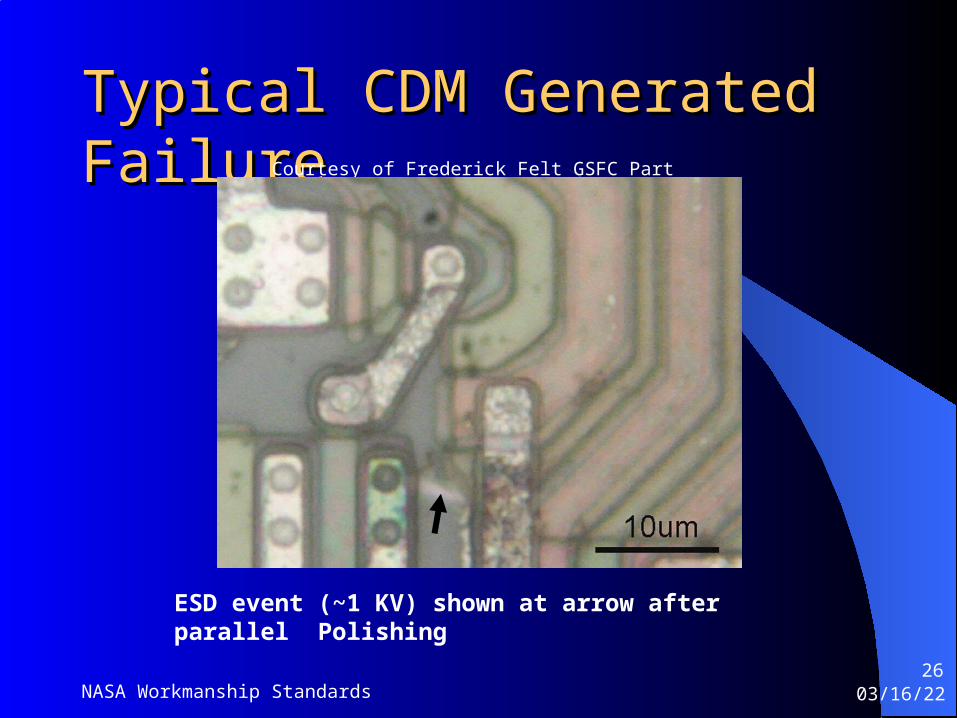
Typical CDM Generated FailureTypical CDM Generated FailureCourtesy of Frederick Felt GSFC Part Analysis Lab.
ESD event (~1 KV) shown at arrow after parallel Polishing