Embed Size (px)
Citation preview
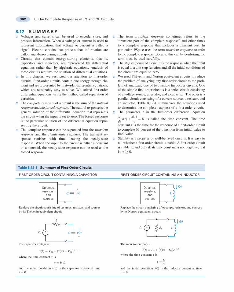
8.12 SUMMARYVoltages and currents can be used to encode, store, andprocess information. When a voltage or current is used torepresent information, that voltage or current is called asignal. Electric circuits that process that information arecalled signal-processing circuits.Circuits that contain energy-storing elements, that is,capacitors and inductors, are represented by differentialequations rather than by algebraic equations. Analysis ofthese circuits requires the solution of differential equations.In this chapter, we restricted our attention to first-ordercircuits. First-order circuits contain one energy storage ele-ment and are represented by first-order differential equations,which are reasonably easy to solve. We solved first-orderdifferential equations, using the method called separation ofvariables.The complete response of a circuit is the sum of the naturalresponse and the forced response. The natural response is thegeneral solution of the differential equation that representsthe circuit when the input is set to zero. The forced responseis the particular solution of the differential equation repre-senting the circuit.The complete response can be separated into the transientresponse and the steady-state response. The transient re-sponse vanishes with time, leaving the steady-stateresponse. When the input to the circuit is either a constantor a sinusoid, the steady-state response can be used as theforced response.
The term transient response sometimes refers to the“transient part of the complete response” and other timesto a complete response that includes a transient part. Inparticular, PSpice uses the term transient response to referto the complete response. Because this can be confusing, theterm must be used carefully.The step response of a circuit is the response when the inputis equal to a unit step function and all the initial conditions ofthe circuit are equal to zero.We used Th!evenin and Norton equivalent circuits to reducethe problem of analyzing any first-order circuit to the prob-lem of analyzing one of two simple first-order circuits. Oneof the simple first-order circuits is a series circuit consistingof a voltage source, a resistor, and a capacitor. The other is aparallel circuit consisting of a current source, a resistor, andan inductor. Table 8.12-1 summarizes the equations usedto determine the complete response of a first-order circuit.The parameter t in the first-order differential equationddt
x tð Þ þ x tð Þt
¼ K is called the time constant. The time
constant t is the time for the response of a first-order circuitto complete 63 percent of the transition from initial value tofinal value.Stability is a property of well-behaved circuits. It is easy totell whether a first-order circuit is stable. A first-order circuitis stable if, and only if, its time constant is not negative, thatis, t + 0.
Table 8.12-1 Summary of First-Order Circuits
FIRST-ORDER CIRCUIT CONTAINING A CAPACITOR FIRST-ORDER CIRCUIT CONTAINING AN INDUCTOR
v(t)C+
–
Op amps,resistors,
andsources
L
i(t)Op amps,resistors,
andsources
Replace the circuit consisting of op amps, resistors, and sourcesby its Th!evenin equivalent circuit:
Replace the circuit consisting of op amps, resistors, and sourcesby its Norton equivalent circuit:
v(t)Voc
Rt
C+
–
+–
Isc Rt L
i(t)
The capacitor voltage is:
v tð Þ ¼ Voc þ v 0ð Þ & Vocð Þe&t=t
where the time constant t is
t ¼ RtC
and the initial condition v(0) is the capacitor voltage at timet ¼ 0.
The inductor current is
i tð Þ ¼ Isc þ i 0ð Þ & Iscð Þe&t=t
where the time constant t is
t ¼ LRt
and the initial condition i(0) is the inductor current at timet ¼ 0.
362 8. The Complete Response of RL and RC Circuits
PROBLEMS
Section 8.3 The Response of a First-Order Circuit toa Constant Input
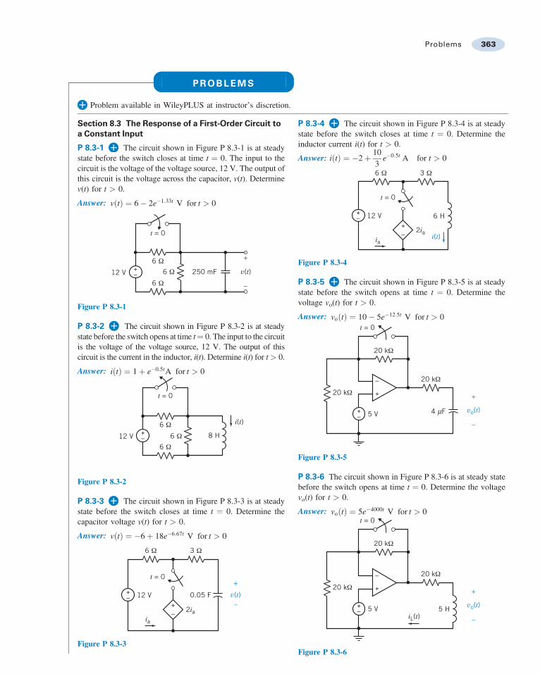
P 8.3-1 The circuit shown in Figure P 8.3-1 is at steadystate before the switch closes at time t ¼ 0. The input to thecircuit is the voltage of the voltage source, 12 V. The output ofthis circuit is the voltage across the capacitor, v(t). Determinev(t) for t > 0.
Answer: v tð Þ ¼ 6 & 2e&1:33t V for t > 0
+– v(t)
+
–
6 Ω
6 Ω12 V 6 Ω
t = 0
250 mF
Figure P 8.3-1
P 8.3-2 The circuit shown in Figure P 8.3-2 is at steadystate before the switch opens at time t¼ 0. The input to the circuitis the voltage of the voltage source, 12 V. The output of thiscircuit is the current in the inductor, i(t). Determine i(t) for t > 0.
Answer: i tð Þ ¼ 1 þ e&0:5tA for t > 0
+–
6 Ω
6 Ω12 V 6 Ω 8 H
t = 0
i(t)
Figure P 8.3-2
P 8.3-3 The circuit shown in Figure P 8.3-3 is at steadystate before the switch closes at time t ¼ 0. Determine thecapacitor voltage v(t) for t > 0.
Answer: v tð Þ ¼ &6 þ 18e&6:67t V for t > 0
6 Ω 3 Ω
ia
v(t)
+
–
+– 0.05 F
t = 0
12 V+– 2ia
Figure P 8.3-3
P 8.3-4 The circuit shown in Figure P 8.3-4 is at steadystate before the switch closes at time t ¼ 0. Determine theinductor current i(t) for t > 0.
Answer: i tð Þ ¼ &2 þ 103
e&0:5t A for t > 0
6 Ω 3 Ω
iai(t)
+– 6 H
t = 0
12 V+– 2ia
Figure P 8.3-4
P 8.3-5 The circuit shown in Figure P 8.3-5 is at steadystate before the switch opens at time t ¼ 0. Determine thevoltage vo(t) for t > 0.
Answer: vo tð Þ ¼ 10 & 5e&12:5t V for t > 0
+
–
+
–
+–
vo(t)
t = 0
20 kΩ
20 kΩ
4 mF
20 kΩ
5 V
Figure P 8.3-5
P 8.3-6 The circuit shown in Figure P 8.3-6 is at steady statebefore the switch opens at time t ¼ 0. Determine the voltagevo(t) for t > 0.
Answer: vo tð Þ ¼ 5e&4000t V for t > 0
+
–
+
–
+–
vo(t)
iL(t)
t = 0
20 kΩ
20 kΩ
20 kΩ
5 V 5 H
Figure P 8.3-6
Problem available in WileyPLUS at instructor’s discretion.
Problems 363
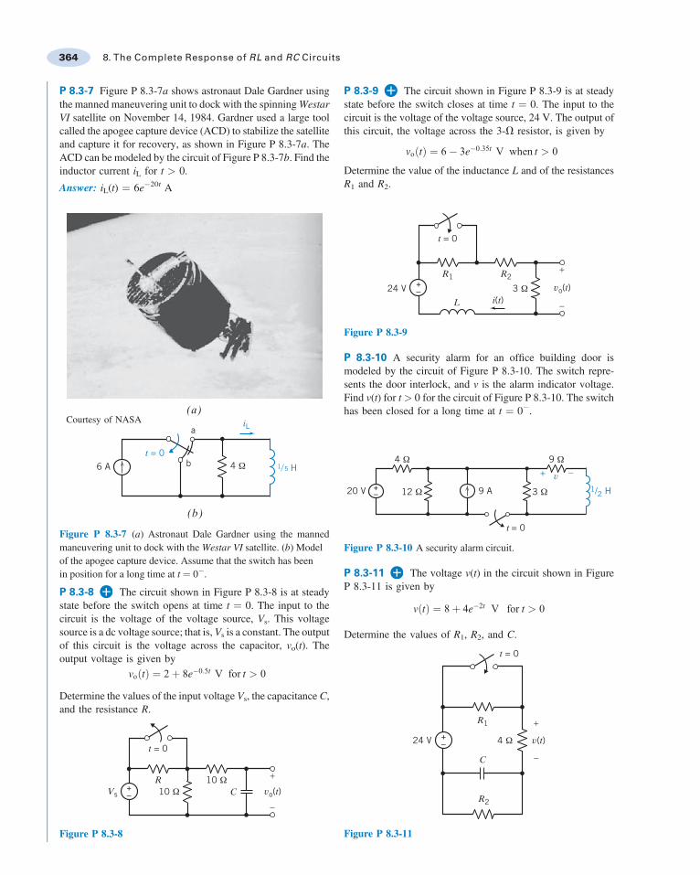
P 8.3-7 Figure P 8.3-7a shows astronaut Dale Gardner usingthe manned maneuvering unit to dock with the spinning WestarVI satellite on November 14, 1984. Gardner used a large toolcalled the apogee capture device (ACD) to stabilize the satelliteand capture it for recovery, as shown in Figure P 8.3-7a. TheACD can be modeled by the circuit of Figure P 8.3-7b. Find theinductor current iL for t > 0.
Answer: iL(t) ¼ 6e&20t A
1 5 H4 Ωt = 0
6 A
a
b
iL
(b)
(a)
Figure P 8.3-7 (a) Astronaut Dale Gardner using the mannedmaneuvering unit to dock with the Westar VI satellite. (b) Modelof the apogee capture device. Assume that the switch has beenin position for a long time at t ¼ 0&.
P 8.3-8 The circuit shown in Figure P 8.3-8 is at steadystate before the switch opens at time t ¼ 0. The input to thecircuit is the voltage of the voltage source, Vs. This voltagesource is a dc voltage source; that is, Vs is a constant. The outputof this circuit is the voltage across the capacitor, vo(t). Theoutput voltage is given by
vo tð Þ ¼ 2þ 8e&0:5t V for t > 0
Determine the values of the input voltage Vs, the capacitance C,and the resistance R.
+–
RVs 10 Ω
10 Ω
t = 0
C vo(t)
+
–
Figure P 8.3-8
P 8.3-9 The circuit shown in Figure P 8.3-9 is at steadystate before the switch closes at time t ¼ 0. The input to thecircuit is the voltage of the voltage source, 24 V. The output ofthis circuit, the voltage across the 3-V resistor, is given by
vo tð Þ ¼ 6& 3e&0:35t V when t > 0
Determine the value of the inductance L and of the resistancesR1 and R2.
+–
R1
L
R2
t = 0
vo(t)
+
–
3 Ω24 Vi(t)
Figure P 8.3-9
P 8.3-10 A security alarm for an office building door ismodeled by the circuit of Figure P 8.3-10. The switch repre-sents the door interlock, and v is the alarm indicator voltage.Find v(t) for t > 0 for the circuit of Figure P 8.3-10. The switchhas been closed for a long time at t ¼ 0&.
v+ –
1/2 H
4 Ω 9 Ω
12 Ω 3 Ω+–20 V 9 A
t = 0
Figure P 8.3-10 A security alarm circuit.
P 8.3-11 The voltage v(t) in the circuit shown in FigureP 8.3-11 is given by
v tð Þ ¼ 8þ 4e&2t V for t > 0
Determine the values of R1, R2, and C.
t = 0
24 V 4 Ω v(t)
C
R1
R2
+–
+
–
Figure P 8.3-11
Courtesy of NASA
364 8. The Complete Response of RL and RC Circuits
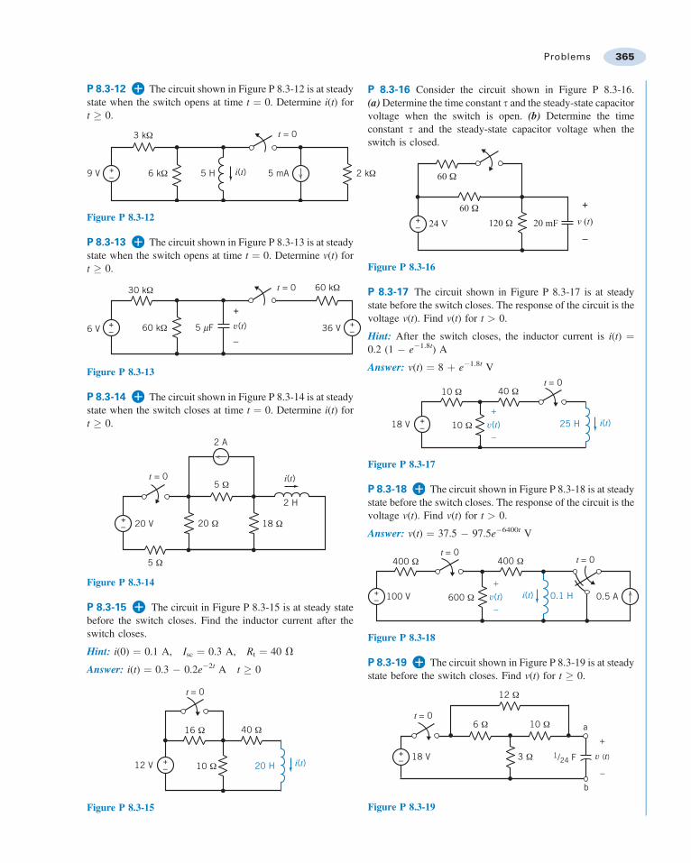
P 8.3-12 The circuit shown in Figure P 8.3-12 is at steadystate when the switch opens at time t ¼ 0. Determine i(t) fort + 0.
3 kΩ
2 kΩ6 kΩ9 V 5 H 5 mAi(t)
t = 0
+–
Figure P 8.3-12
P 8.3-13 The circuit shown in Figure P 8.3-13 is at steadystate when the switch opens at time t ¼ 0. Determine v(t) fort + 0.
30 kΩ 60 kΩ
60 kΩ6 V 36 V5 mF
t = 0
+–
+–
+
–v(t)
Figure P 8.3-13
P 8.3-14 The circuit shown in Figure P 8.3-14 is at steadystate when the switch closes at time t ¼ 0. Determine i(t) fort + 0.
20 V
2 H
2 A
20 Ω
5 Ω
18 Ω
5 Ωt = 0 i(t)
+–
Figure P 8.3-14
P 8.3-15 The circuit in Figure P 8.3-15 is at steady statebefore the switch closes. Find the inductor current after theswitch closes.
Hint: i(0) ¼ 0.1 A, Isc ¼ 0.3 A, Rt ¼ 40 V
Answer: i(t) ¼ 0.3 & 0.2e&2t A t + 0
i(t)
16 Ω
10 Ω
40 Ω
+–12 V 20 H
t = 0
Figure P 8.3-15
P 8.3-16 Consider the circuit shown in Figure P 8.3-16.(a) Determine the time constant t and the steady-state capacitorvoltage when the switch is open. (b) Determine the timeconstant t and the steady-state capacitor voltage when theswitch is closed.
+–
+
–
v (t)
60 Ω
60 Ω 120 Ω 24 V 20 mF
Figure P 8.3-16
P 8.3-17 The circuit shown in Figure P 8.3-17 is at steadystate before the switch closes. The response of the circuit is thevoltage v(t). Find v(t) for t > 0.
Hint: After the switch closes, the inductor current is i(t) ¼0.2 (1 & e&1.8t) A
Answer: v(t) ¼ 8 þ e&1.8t V
i(t)10 Ω 25 Hv(t)+
–
10 Ω 40 Ω
+–18 V
t = 0
Figure P 8.3-17
P 8.3-18 The circuit shown in Figure P 8.3-18 is at steadystate before the switch closes. The response of the circuit is thevoltage v(t). Find v(t) for t > 0.
Answer: v(t) ¼ 37.5 & 97.5e&6400t V
i(t)600 Ω 0.1 Hv(t)+
–
400 Ω 400 Ω
+– 100 V 0.5 A
t = 0t = 0
Figure P 8.3-18
P 8.3-19 The circuit shown in Figure P 8.3-19 is at steadystate before the switch closes. Find v(t) for t + 0.
+–
12 Ω
6 Ω
3 Ω
a
b
18 V
10 Ω
v (t)
+
–
1/24 F
t = 0
Figure P 8.3-19
Problems 365
P 8.3-20 The circuit shown in Figure P 8.3-20 is at steadystate before the switch closes. Determine i(t) for t + 0.
5 Ω 20 Ω
20 Ω20 Ω
3.5 H+– 24 V
i(t)
t = 0
Figure P 8.3-20
P 8.3-21 The circuit in Figure P 8.3-21 is at steady state beforethe switch closes. Determine an equation that represents thecapacitor voltage after the switch closes.
+– 18 V
+
–
25 mF
10 Ω
40 Ω
t = 0
v (t)
Figure P 8.3-21
P 8.3-22 The circuit shown in Figure P 8.3-22 is at steady statewhen the switch closes at time t ¼ 0. Determine i(t) for t + 0.
2 A 4 A
5 Ω
3 Ω
8 Ω
a
b
i(t)2 H
t = 0
Figure P 8.3-22
P 8.3-23 The circuit in Figure P 8.3-23 is at steady state beforethe switch closes. Determine an equation that represents theinductor current after the switch closes.
7 A
2.5 Ht = 0 i (t)
60 Ω20 Ω
Figure P 8.3-23
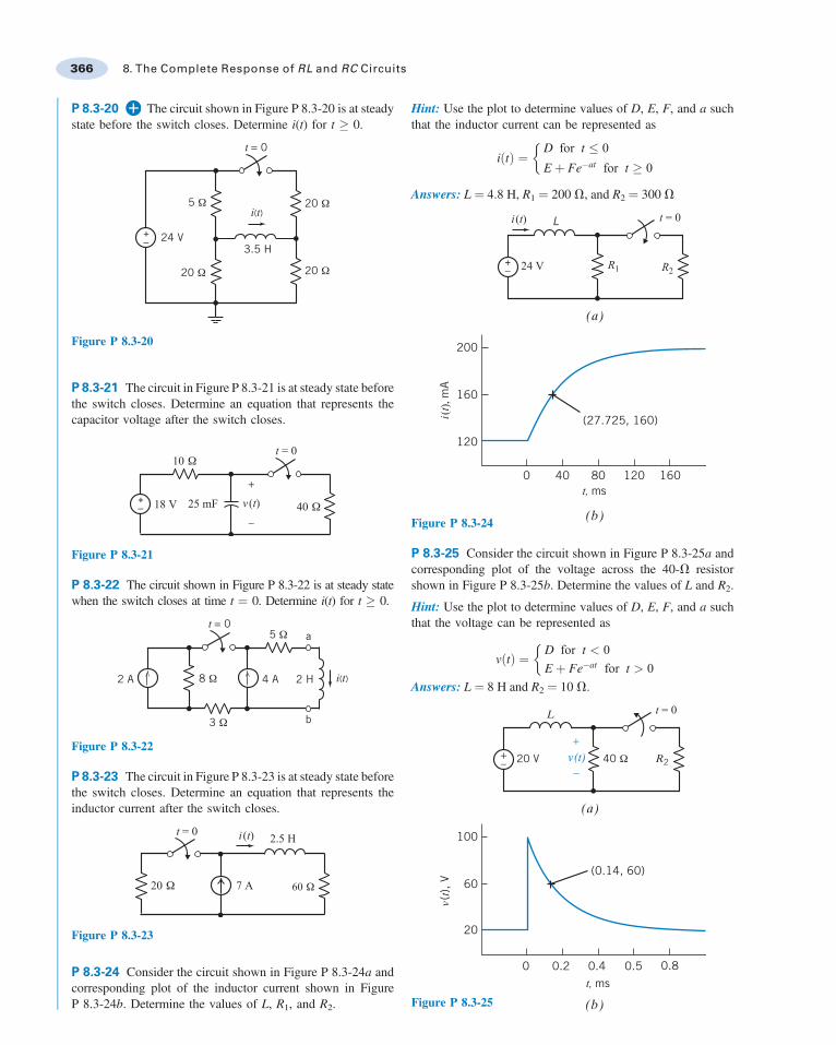
P 8.3-24 Consider the circuit shown in Figure P 8.3-24a andcorresponding plot of the inductor current shown in FigureP 8.3-24b. Determine the values of L, R1, and R2.
Hint: Use the plot to determine values of D, E, F, and a suchthat the inductor current can be represented as
i tð Þ ¼D for t , 0
E þ Fe&at for t + 0
(
Answers: L ¼ 4.8 H, R1 ¼ 200 V, and R2 ¼ 300 V
i (t)
i(t),
mA
t, ms
t = 0
24 V
200
(27.725, 160)
160
0 40 80 120
120
160
R1 R2
L
+–
(b)
(a)
Figure P 8.3-24
P 8.3-25 Consider the circuit shown in Figure P 8.3-25a andcorresponding plot of the voltage across the 40-V resistorshown in Figure P 8.3-25b. Determine the values of L and R2.
Hint: Use the plot to determine values of D, E, F, and a suchthat the voltage can be represented as
v tð Þ ¼D for t < 0E þ Fe&at for t > 0
(
Answers: L ¼ 8 H and R2 ¼ 10 V.
40 Ω20 V
L
–+ v(t)
+
t = 0
–
(a)
(b)
0
v(t),
V
100
60
0.80.5
(0.14, 60)
0.40.2t, ms
20
Figure P 8.3-25
366 8. The Complete Response of RL and RC Circuits
P 8.3-26 Determine vo(t) for t> 0 for the circuit shown inFigure P 8.3-26.
18 Ω18 Ω
2.4 mA 18 Ω
0.8 H
0.7 H
v o (t )
+
–
Figure P 8.3-26
P 8.3-27 The circuit shown in Figure P 8.3-27 is at steadystate before the switch closes at time t ¼ 0. After the switchcloses, the inductor current is given by
i tð Þ ¼ 0:6& 0:2e&5t A for t + 0
Determine the values of R1, R2, and L.
Answers: R1 ¼ 20 V, R2 ¼ 10 V, and L ¼ 4 H
i(t)+–
t = 0
L
R2
R1
12 V
Figure P 8.3-27
P 8.3-28 After time t ¼ 0, a given circuit is represented bythe circuit diagram shown in Figure P 8.3-28.
(a) Suppose that the inductor current is
i tð Þ ¼ 21:6þ 28:4e&4t mA for t + 0
Determine the values of R1 and R3.(b) Suppose instead that R1 ¼ 16 V, R3 ¼ 20 V, and the initial
condition is i(0) ¼ 10 mA.Determine the inductor current for t + 0.
36 mA 2 HR1
4 Ω
R3
i(t)
Figure P 8.3-28
P 8.3-29 Consider the circuit shown in Figure P 8.3-29.
(a) Determine the time constant t and the steady-statecapacitor voltage v(1) when the switch is open.
(b) Determine the time constant t and the steady-state capaci-tor voltage v(1) when the switch is closed.
Answers: (a) t ¼ 3 s, and v(1) ¼ 24 V; (b) t ¼ 2.25 s, andv(1) ¼ l2 V
50 Ω 50 Ω50 Ω
v(t)
+
–
+– 24 V 90 mF
Figure P 8.3-29
Section 8.4 Sequential Switching
P 8.4-1 The circuit shown in Figure P 8.4-1 is at steadystate before the switch closes at time t ¼ 0. The switch remainsclosed for 1.5 s and then opens. Determine the capacitor voltagev(t) for t > 0.
Hint: Determine v(t) when the switch is closed. Evaluate v(t) attime t ¼ 1.5 s to get v(1.5). Use v(1.5) as the initial condition todetermine v(t) after the switch opens again.
Answer: v tð Þ ¼ 5 þ 5e&5t V for 0 < t < 1:5 s10 & 2:64e&2:5 t&1:5ð Þ V for 1:5 s < t
(
8 Ω
8 Ω
v(t)
+
–
+– 0.05 F
t = 0 t = 1.5 s
10 V
Figure P 8.4-1
P 8.4-2 The circuit shown in Figure P 8.4-2 is at steadystate before the switch closes at time t ¼ 0. The switch remainsclosed for 1.5 s and then opens. Determine the inductor currenti(t) for t > 0.
Answer: v tð Þ ¼2 þ e&0:5t A for 0 < t < 1:5 s
3 & 0:53e&0:667 t&1:5ð Þ A for 1:5 s < t
(
4 Ω 4 Ω
4 Ω
12 H
t = 0 t = 1.5 s
24 V i(t)+–
Figure P 8.4-2
P 8.4-3 Cardiac pacemakers are used by people to maintainregular heart rhythm when they have a damaged heart. Thecircuit of a pacemaker can be represented as shown in FigureP 8.4-3. The resistance of the wires, R, can be neglected becauseR < 1 mV. The heart’s load resistance RL is 1 kV. The firstswitch is activated at t¼ t0, and the second switch is activated at t1¼ t0 þ 10 ms. This cycle is repeated every second. Find v(t) for t0, t , 1. Note that it is easiest to consider t0 ¼ 0 for this
Problems 367
calculation. The cycle repeats by switch 1 returning to position aand switch 2 returning to its open position.
Hint: Use q ¼ Cv to determine v(0&) for the 100-mF capacitor.
+–
R R
t = t0t = t1
vRL
Switch 1
+
–
a
Switch 2
The heart
100 mF400 mF3 V
Figure P 8.4-3
P 8.4-4 An electronic flash on a camera uses the circuitshown in Figure P 8.4-4. Harold E. Edgerton invented theelectronic flash in 1930. A capacitor builds a steady-statevoltage and then discharges it as the shutter switch is pressed.The discharge produces a very brief light discharge. Determinethe elapsed time t1 to reduce the capacitor voltage to one-half ofits initial voltage. Find the current i(t) at t ¼ t1.
5 V 100 kΩ+–
t = 0
1 mF
Figure P 8.4-4 Electronic flash circuit.
P 8.4-5 The circuit shown in Figure P 8.4-5 is at steadystate before the switch opens at t ¼ 0. The switch remains openfor 0.5 second and then closes. Determine v(t) for t + 0.
24 V 50 mF
40 Ω
40 Ω 10 Ωv(t)
t = 0.5 s
t = 0 s+–
+
–
Figure P 8.4-5
Section 8.5 Stability of First-Order Circuits
P 8.5-1 The circuit in Figure P 8.5-1 contains a currentcontrolled voltage source. What restriction must be placed onthe gain R of this dependent source to guarantee stability?
Answer: R < 400 V
5 mH
100 Ω
400 Ω+–
iL(t)
Ri(t)
i(t)4 + 8u(t) V
+ –
Figure P 8.5-1
P 8.5-2 The circuit in Figure P 8.5-2 contains a current-controlled current source. What restriction must beplaced on the gain B of this dependent source to guaranteestability?
5 mH6 kΩ
3 kΩ+–
iL(t)Bi(t)
i(t)
4 + 8u(t) V
Figure P 8.5-2
Section 8.6 The Unit Step Source
P 8.6-1 The input to the circuit shown in Figure P 8.6-1 isthe voltage of the voltage source, vs(t). The output is the voltageacross the capacitor, vo(t). Determine the output of this circuitwhen the input is vs(t) ¼ 8 & 15 u(t) V.
vs(t)+–
6 Ω
vo(t)+
–66.7 µF
Figure P 8.6-1
P 8.6-2 The input to the circuit shown in Figure P 8.6-2is the voltage of the voltage source, vs(t). The output is thevoltage across the capacitor, vo(t). Determine the output of thiscircuit when the input is vs(t) ¼ 3 þ 3 u(t) V.
vs(t)+–
3 Ω
6 Ω vo(t)+
–500 mF
Figure P 8.6-2
P 8.6-3 The input to the circuit shown in Figure P 8.6-3 isthe voltage of the voltage source, vs(t). The output is the currentin the inductor, io(t). Determine the output of this circuit whenthe input is vs(t) ¼ &7 þ 13 u(t) V.
vs(t)+–
5 Ω
4 Ω 1.2 Hio(t)
Figure P 8.6-3
368 8. The Complete Response of RL and RC Circuits
P 8.6-4 Determine vo(t) for t> 0 for the circuit shown inFigure P 8.6-4.
–
+
30 kΩ 45 kΩ
v o (t )2.4 + 1.2 u (t ) V
20 kΩ
+–
+
–5 mF
Figure P 8.6-4
P 8.6-5 The initial voltage of the capacitor of the circuitshown in Figure P 8.6-5 is zero. Determine the voltage v(t)when the source is a pulse, described by
vs ¼0 t < 1 s
4 V 1 < t < 2 s
0 t > 2 s
8><
>:
v+
–vs
Ω500 k
2 F+–
Figure P 8.6-5
P 8.6-6 Studies of an artificial insect are being used tounderstand the nervous system of animals. A model neuronin the nervous system of the artificial insect is shown in FigureP 8.6-6. A series of pulses, called synapses, is required.The switch generates a pulse by opening at t ¼ 0 and closingat t ¼ 0.5 s. Assume that the circuit is in steady state andthat v(0&) ¼ 10 V. Determine the voltage v(t) for 0 < t < 2 s.
+– v
+
–
Ω6
Ω3
Switch
30 V F1 6
Figure P 8.6-6 Neuron circuit model.
P 8.6-7 Determine the voltage vo(t) in the circuit shown inFigure P 8.6-7.
+–
25 Ωi L
v o
+
_
15 Ω10 Ω2 − 8u (t ) V
4 H
Figure P 8.6-7
P 8.6-8 Determine vc(t) for t > 0 for the circuit of FigureP 8.6-8.
+–
4 kΩ
3 kΩ
4 kΩ
vc12u(t) V
+
–
–
+2 mA 50 Fµ
Figure P 8.6-8
P 8.6-9 The voltage source voltage in the circuit shown inFigure P 8.6-9 is
vs tð Þ ¼ 7& 14u tð Þ V
Determine v(t) for t > 0.
–
–
++
5 Ω3 Ω v(t)vS(t)
0.46 F
Figure P 8.6-9
P 8.6-10 Determine the voltage v(t) for t+ 0 for the circuitshown in Figure P 8.6-10.
–
+
a
b
30 Ω120 Ω
96 Ω 32 Ω
5 + 15u(t)
–+ 12.5 mF v(t)
Figure P 8.6-10
P 8.6-11 The voltage source voltage in the circuit shown inFigure P 8.6-11 is
vs tð Þ ¼ 5þ 20u tð Þ
Determine i(t) for t + 0.
i(t)vs(t)ib 4 ib 25 H
a
b
10 kΩ5 kΩ
+–
Figure P 8.6-11
Problems 369
P 8.6-12 The voltage source voltage in the circuit shown inFigure P 8.6-12 is
vs tð Þ ¼ 12& 6u tð ÞV
Determine v(t) for t + 0.
+–
8 Ω
4 Ω
a
b
va
0.75va
–
–+
+v(t)3/40 Fvs(t)
Figure P 8.6-12
P 8.6-13 Determine i(t) for t + 0 for the circuit shown inFigure P 8.6-13.
3 Ω2.5 u(t) A6 Ω
4 Ω 1 Ω2ix
a
b
+ –
ix i(t)5 H
Figure P 8.6-13
P 8.6-14 Determine i(t) for t + 0 for the circuit shown inFigure P 8.6-14.
100 Ω150 Ω
2 V+–
+–i(t)2 H6u(t) V
Figure P 8.6-14
P 8.6-15 Determine v(t) for t + 0 for the circuit shown inFigure P 8.6-15.
20 Ω
8 Ω a
10 Ω
120 Ω 50 Ω
b
20u(t)Av(t)1 mF
+
–
Figure P 8.6-15
P 8.6-16 Determine v(t) for t + 0 for the circuit shown inFigure P 8.6-16.
20 mF20 V
2 u(t) A
20 Ω
5 Ω5 Ω 4 Ω
b
a
18 Ω
–
+
v(t)–+
Figure P 8.6-16
P 8.6-17 Determine i(t) for t + 0 for the circuit shown inFigure P 8.6-17.
2 H
i(t)
24 Ω
18 Ω12 u(t) V
24 Ω
12 Ω2 A+–
Figure P 8.6-17
P 8.6-18 The voltage source voltage in the circuit shown inFigure P 8.6-18 is
vs tð Þ ¼ 8þ 12u tð ÞV
Determine v(t) for t + 0.
vs(t) v(t)160 Ω40 Ω 18 Ω
3 mF 5 mF+–
+
–
Figure P 8.6-18
P 8.6-19 Determine the current io(t) in the circuit shown inFigure P 8.6-19.
3 Ω
10 Ω 1 Ω2 i x+ –
i x+–
112 F v c
+
_
i o
5 + 10u (t ) V
Figure P 8.6-19
P 8.6-20 The voltage source voltage in the circuit shownin Figure P 8.6-20 is
vs tð Þ ¼ 25u tð Þ & 10 V
370 8. The Complete Response of RL and RC Circuits
Determine i(t) for t + 0.
100 Ω40 Ω150 Ω
12 H
8 H
i(t)vs(t)+–
Figure P 8.6-20
P 8.6-21 The voltage source voltage in the circuit shown inFigure P 8.6-21 is
vs tð Þ ¼ 30& 24u tð ÞVDetermine i(t) for t + 0.
100 Ω
100 Ω
50 Ω
20 H 5 H
i(t)
vs(t) +–
Figure P 8.6-21
P 8.6-22 The voltage source voltage in the circuit shown inFigure P 8.6-22 is
vs tð Þ ¼ 10þ 40u tð ÞV
Determine v(t) for t + 0.
5 Ω
5 Ω40 Ωvs(t)
100 mF
150 mFv(t)+–
+
–
Figure P 8.6-22
P 8.6-23 Determine v(t) for t > 0 for the circuit shown inFigure P 8.6-23.
12 u(t)
6 Ω
2 Ω
3 Ω
12 Ω
3 H
v(t)+–
+
–
Figure P 8.6-23
P 8.6-24 The input to the circuit shown in Figure P 8.6-24is the current source current
is tð Þ ¼ 2þ 4u tð ÞAThe output is the voltage v(t). Determine v(t) for t > 0.
is(t) v(t) 3 Ω
3 Ω
3 Ω 0.25 H
+
–
Figure P 8.6-24
P 8.6-25 The input to the circuit shown in Figure P 8.6-25is the voltage source voltage
vs ¼ 6þ 6u tð ÞThe output is the voltage vo(t). Determine vo(t) for t > 0.
0.125 F 10 Ω
6 Ω 2 Ωvs(t) vo(t)+–
+
–
Figure P 8.6-25
P 8.6-26 Determine v(t) for t > 0 for the circuit shown inFigure P 8.6-26.
0.5 H
3 Ω
4 Ω2 Ω v(t)
12 u(t) +–
+
–
Figure P 8.6-26
P 8.6-27 When the input to the circuit shown in FigureP 8.6-27 is the voltage source voltage
vs tð Þ ¼ 3& u tð ÞV
The output is the voltage
vo tð Þ ¼ 10þ 5 e&50t V for t + 0
Determine the values of R1 and R2.
+– vs(t)
vo(t)
+
–
+
–
R1
R2
–
+
v(t)C = 1 mF 1 kΩ
Figure P 8.6-27
Problems 371
P 8.6-28 The time constant of a particular circuit is t¼ 0.25 s.In response to a step input, a capacitor voltage changesfrom &2.5 V to 4.2 V. How long did it take for the capacitorvoltage to increase from &2.0 V to þ2.0 V?
Section 8.7 The Response of a First-Order Circuit toa Nonconstant Source
P 8.7-1 Find vc(t) for t > 0 for the circuit shown in FigureP 8.7-1 when v1 ¼ 8e&5tu(t) V. Assume the circuit is in steadystate at t ¼ 0&.
Answer: vc(t) ¼ 4e&9t þ 18e&5t V
–vc
+ +–
+–3 Ω
1/36 F2ix
ixv1
12 Ω 38.5 V
t = 0
Figure P 8.7-1
P 8.7-2 Find v(t) for t > 0 for the circuit shown in FigureP 8.7-2. Assume steady state at t ¼ 0&.
Answer: v(t) ¼ 20e&10t/3 & 12e&2t V
+–
4 Ω
12 V 2/5 H v
+
–
2 Ω 6 e–2t u(t) A
Figure P 8.7-2
P 8.7-3 Find vc(t) for t > 0 for the circuit shown in FigureP 8.7-3 when is ¼ [2 cos 2t] u(t) mA.
vc+
–1/30 mF
10 kΩ
5 kΩis
Figure P 8.7-3
P 8.7-4 Many have witnessed the use of an electrical mega-phone for amplification of speech to a crowd. A model of amicrophone and speaker is shown in Figure P 8.7-4a, and thecircuit model is shown in Figure P 8.7-4b. Find v(t) for vs ¼ 10(sin 100t)u(t), which could represent a person whistling orsinging a pure tone.
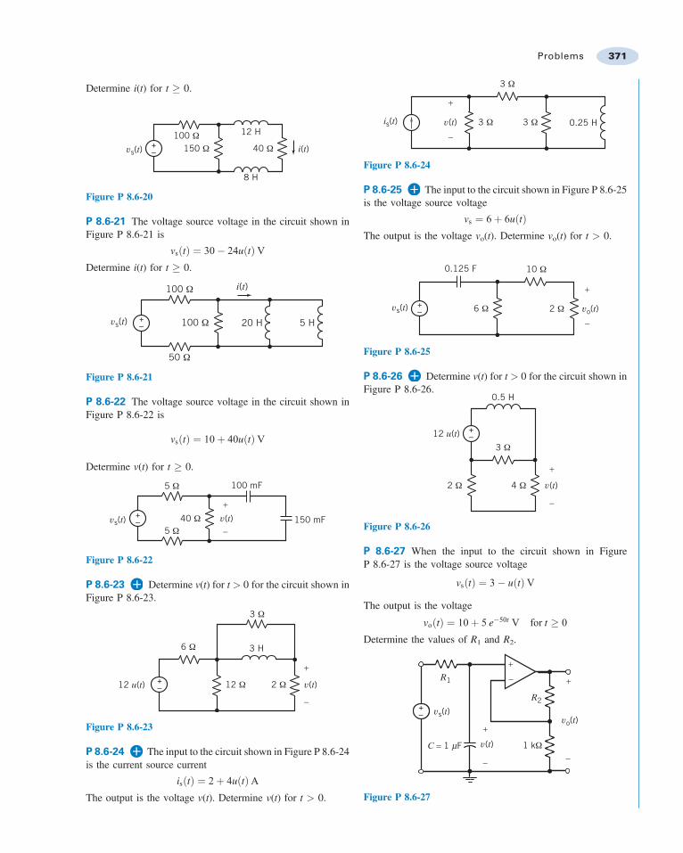
(b)
(a)
8 Ω
1 Ω
++
––
Carbon granulepacket
0.5 H
Speaker
Sound(pressure waves)
Diaphragm
vvs
Figure P 8.7-4 Megaphone circuit.
P 8.7-5 A lossy integrator is shown in Figure P 8.7-5.The lossless capacitor of the ideal integrator circuit hasbeen replaced with a model for the lossy capacitor, namely,a lossless capacitor in parallel with a 1-kV resistor. If vs ¼15e&2tu(t) V and vo(0) ¼ 10 V, find vo(t) for t > 0.
C =
R = 1 kΩ
µF1 4
–
+
15 kΩ
vs vo
+
+ –
–
+–
Figure P 8.7-5 Integrator circuit.
P 8.7-6 Determine v(t) for the circuit shown in FigureP 8.7-6.
4 Ω
+– 30 V +
–+
–v(t)
5 Ω 2 Ω
F e–3tu(t) V1 2
Figure P 8.7-6
372 8. The Complete Response of RL and RC Circuits
P 8.7-7 Determine v(t) for the circuit shown in FigureP 8.7-7a when vs varies as shown in Figure P 8.7-7b. Theinitial capacitor voltage is vc(0) ¼ 0.
vs Ω2
2 Ω
+– v
+
–
Vs
+
–
1 F
(a)
(b)
(V)
t (s)
10
0 2
ix ix
vs
Figure P 8.7-7
P 8.7-8 The electron beam, which is used to draw signals onan oscilloscope, is moved across the face of a cathode-ray tube(CRT) by a force exerted on electrons in the beam. The basicsystem is shown in Figure P 8.7-8a. The force is created from atime-varying, ramp-type voltage applied across the vertical orthe horizontal plates. As an example, consider the simple circuitof Figure P 8.7-8b for horizontal deflection in which thecapacitance between the plates is C.
IntensityFocus
Tracerotation
Beamfinder
CRT control
Horizontalsection
Triggersection
Verticalsection
(b)
(a)
(V)
0
vc(t)+
–
Rs C
S+– v(t) = kt
v(t)
t (ms)
Figure P 8.7-8 Cathode-ray tube beam circuit.
Derive an expression for the voltage across the capaci-tance. If v(t) ¼ kt and Rs ¼ 625 kV, k ¼ 1000, and C ¼ 2000 pF,compute vc as a function of time. Sketch v(t) and vc(t) on thesame graph for time less than 10 ms. Does the voltage acrossthe plates track the input voltage?
Section 8.10 How CanWe Check . . . ?
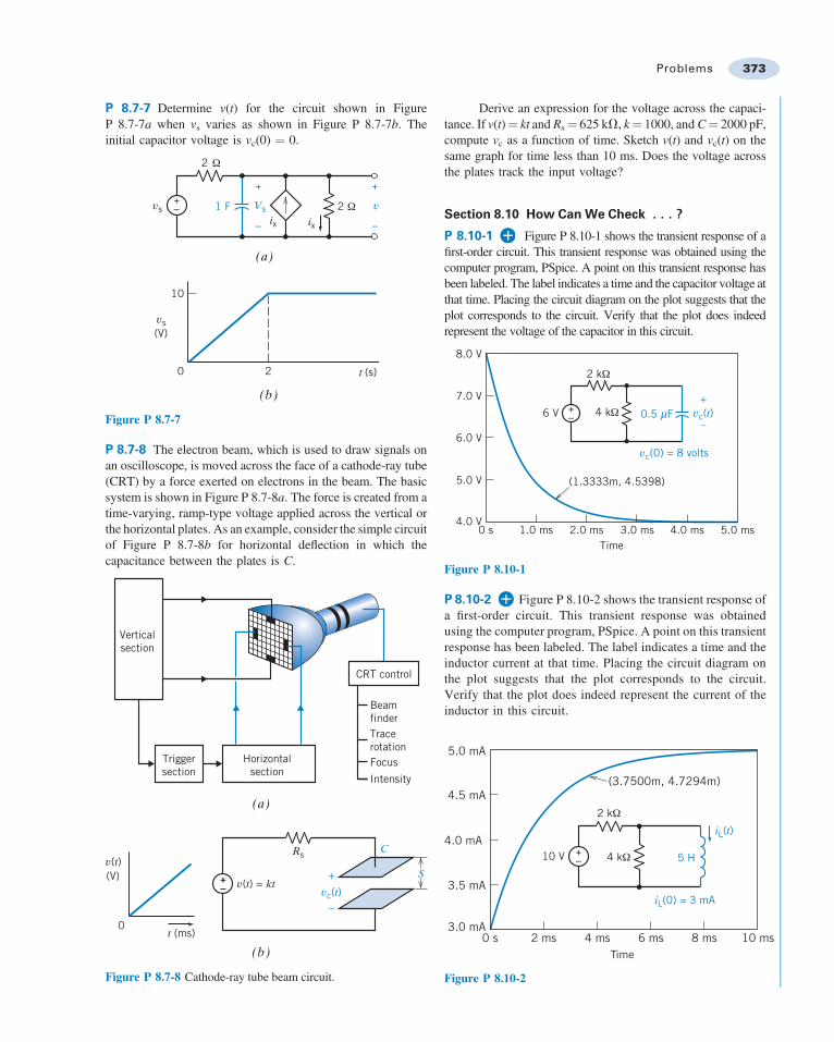
P 8.10-1 Figure P 8.10-1 shows the transient response of afirst-order circuit. This transient response was obtained using thecomputer program, PSpice. A point on this transient response hasbeen labeled. The label indicates a time and the capacitor voltage atthat time. Placing the circuit diagram on the plot suggests that theplot corresponds to the circuit. Verify that the plot does indeedrepresent the voltage of the capacitor in this circuit.
4.0 V0 s 1.0 ms 2.0 ms 3.0 ms
Time
(1.3333m, 4.5398)
6 V
vc(0) = 8 volts
4.0 ms 5.0 ms
5.0 V
6.0 V
7.0 V
8.0 V
+–
+
–vc(t)4 kΩ
2 kΩ
0.5 mF
Figure P 8.10-1
P 8.10-2 Figure P 8.10-2 shows the transient response ofa first-order circuit. This transient response was obtainedusing the computer program, PSpice. A point on this transientresponse has been labeled. The label indicates a time and theinductor current at that time. Placing the circuit diagram onthe plot suggests that the plot corresponds to the circuit.Verify that the plot does indeed represent the current of theinductor in this circuit.
2 kΩ
5 H
3.0 mA
3.5 mA
4.0 mA
4.5 mA
5.0 mA
0 s 2 ms 4 ms 6 ms 8 ms 10 msTime
(3.7500m, 4.7294m)
4 kΩ10 V
iL(0) = 3 mA
+–
iL(t)
Figure P 8.10-2
Problems 373
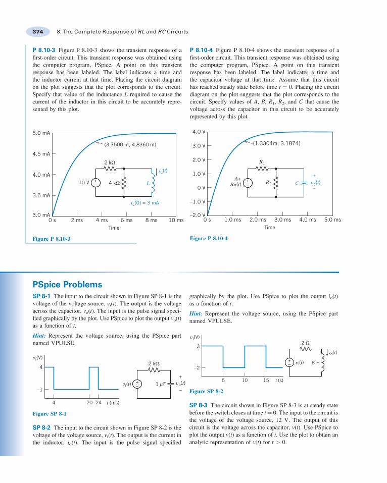
P 8.10-3 Figure P 8.10-3 shows the transient response of afirst-order circuit. This transient response was obtained usingthe computer program, PSpice. A point on this transientresponse has been labeled. The label indicates a time andthe inductor current at that time. Placing the circuit diagramon the plot suggests that the plot corresponds to the circuit.Specify that value of the inductance L required to cause thecurrent of the inductor in this circuit to be accurately repre-sented by this plot.
2 kΩ
L
3.0 mA
3.5 mA
4.0 mA
4.5 mA
5.0 mA
0 s 2 ms 4 ms 6 ms 8 ms 10 msTime
(3.7500 m, 4.8360 m)
4 kΩ10 V
iL(0) = 3 mA
+–
iL(t)
Figure P 8.10-3
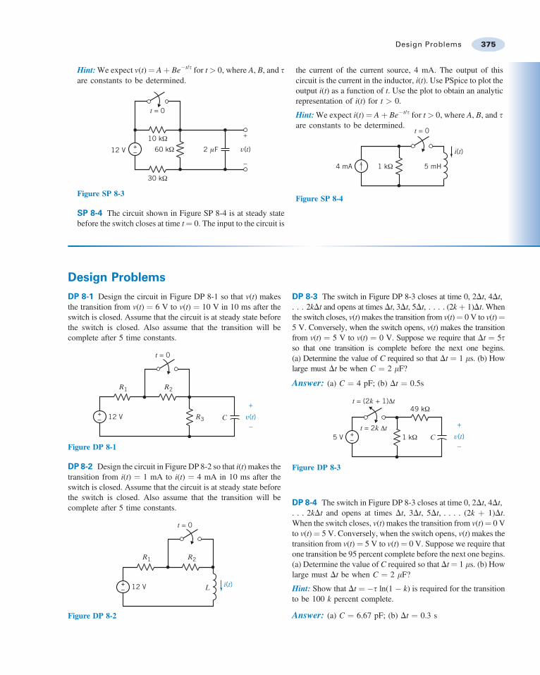
P 8.10-4 Figure P 8.10-4 shows the transient response of afirst-order circuit. This transient response was obtained usingthe computer program, PSpice. A point on this transientresponse has been labeled. The label indicates a time andthe capacitor voltage at that time. Assume that this circuithas reached steady state before time t ¼ 0. Placing the circuitdiagram on the plot suggests that the plot corresponds to thecircuit. Specify values of A, B, R1, R2, and C that cause thevoltage across the capacitor in this circuit to be accuratelyrepresented by this plot.
C
–2.0 V
0 V
–1.0 V
1.0 V
2.0 V
3.0 V
4.0 V
0 s 1.0 ms 2.0 ms 3.0 ms 4.0 ms 5.0 msTime
(1.3304m, 3.1874)
A+Bu(t)
+–
R1
R2 vc(t)+
–
Figure P 8.10-4
PSpice ProblemsSP 8-1 The input to the circuit shown in Figure SP 8-1 is thevoltage of the voltage source, vi(t). The output is the voltageacross the capacitor, vo(t). The input is the pulse signal speci-fied graphically by the plot. Use PSpice to plot the output vo(t)as a function of t.
Hint: Represent the voltage source, using the PSpice partnamed VPULSE.
vo(t)+
–
4
vi(V)
t (ms)4 20 24
–1vi(t)
+–
2 kΩ
1 µF
Figure SP 8-1
SP 8-2 The input to the circuit shown in Figure SP 8-2 is thevoltage of the voltage source, vi(t). The output is the current inthe inductor, io(t). The input is the pulse signal specified
graphically by the plot. Use PSpice to plot the output io(t)as a function of t.
Hint: Represent the voltage source, using the PSpice partnamed VPULSE.
3
vi(V)
t (s)5 10 15
–2vi(t)
+–
2 Ω
8 H
io(t)
Figure SP 8-2
SP 8-3 The circuit shown in Figure SP 8-3 is at steady statebefore the switch closes at time t ¼ 0. The input to the circuit isthe voltage of the voltage source, 12 V. The output of thiscircuit is the voltage across the capacitor, v(t). Use PSpice toplot the output v(t) as a function of t. Use the plot to obtain ananalytic representation of v(t) for t > 0.
374 8. The Complete Response of RL and RC Circuits
Hint: We expect v(t) ¼ A þ Be&t/t for t > 0, where A, B, and tare constants to be determined.
+– v(t)
+
–
10 kΩ
30 kΩ
12 V 60 kΩ
t = 0
2 µF
Figure SP 8-3
SP 8-4 The circuit shown in Figure SP 8-4 is at steady statebefore the switch closes at time t ¼ 0. The input to the circuit is
the current of the current source, 4 mA. The output of thiscircuit is the current in the inductor, i(t). Use PSpice to plot theoutput i(t) as a function of t. Use the plot to obtain an analyticrepresentation of i(t) for t > 0.
Hint: We expect i(t) ¼ A þ Be&t/t for t > 0, where A, B, and tare constants to be determined.
1 kΩ4 mA 5 mH
i(t)
t = 0
Figure SP 8-4
Design ProblemsDP 8-1 Design the circuit in Figure DP 8-1 so that v(t) makesthe transition from v(t) ¼ 6 V to v(t) ¼ 10 V in 10 ms after theswitch is closed. Assume that the circuit is at steady state beforethe switch is closed. Also assume that the transition will becomplete after 5 time constants.
+– v(t)
+
–
t = 0
CR3
R2R1
12 V
Figure DP 8-1
DP 8-2 Design the circuit in Figure DP 8-2 so that i(t) makes thetransition from i(t) ¼ 1 mA to i(t) ¼ 4 mA in 10 ms after theswitch is closed. Assume that the circuit is at steady state beforethe switch is closed. Also assume that the transition will becomplete after 5 time constants.
i(t)+–
t = 0
L
R2R1
12 V
Figure DP 8-2
DP 8-3 The switch in Figure DP 8-3 closes at time 0, 2Dt, 4Dt,. . . 2kDt and opens at times Dt, 3Dt, 5Dt, . . . . (2k þ 1)Dt. Whenthe switch closes, v(t) makes the transition from v(t) ¼ 0 V to v(t) ¼5 V. Conversely, when the switch opens, v(t) makes the transitionfrom v(t) ¼ 5 V to v(t) ¼ 0 V. Suppose we require that Dt ¼ 5tso that one transition is complete before the next one begins.(a) Determine the value of C required so that Dt ¼ 1 ms. (b) Howlarge must Dt be when C ¼ 2 mF?
Answer: (a) C ¼ 4 pF; (b) Dt ¼ 0.5s
49 kΩ
1 kΩ+– v(t)
+
–
t = (2k + 1)Δt
t = 2k ΔtC5 V
Figure DP 8-3
DP 8-4 The switch in Figure DP 8-3 closes at time 0, 2Dt, 4Dt,. . . 2kDt and opens at times Dt, 3Dt, 5Dt, . . . . (2k þ 1)Dt.When the switch closes, v(t) makes the transition from v(t) ¼ 0 Vto v(t) ¼ 5 V. Conversely, when the switch opens, v(t) makes thetransition from v(t) ¼ 5 V to v(t) ¼ 0 V. Suppose we require thatone transition be 95 percent complete before the next one begins.(a) Determine the value of C required so that Dt ¼ 1 ms. (b) Howlarge must Dt be when C ¼ 2 mF?
Hint: Show that Dt ¼ &t ln(1 & k) is required for the transitionto be 100 k percent complete.
Answer: (a) C ¼ 6.67 pF; (b) Dt ¼ 0.3 s
Design Problems 375
DP 8-5 A laser trigger circuit is shown in Figure DP 8-5. Totrigger the laser, we require 60 mA < jij < 180 mA for 0 < t <200 ms. Determine a suitable value for R1 and R2.
+–
t = 0
20 V
i
Ω40
R1R2
Ω40
10 mH Lasertrigger
Figure DP 8-5 Laser trigger circuit.
DP 8-6 Fuses are used to open a circuit when excessive currentflows (Wright, 1990). One fuse is designed to open when thepower absorbed by R exceeds 10 W for 0.5 s. Consider the circuitshown in Figure DP 8-6. The input is given by vs ¼ A[u(t) & u(t &0.75)] V. Assume that iL(0&) ¼ 0. Determine the largest value of Athat will not cause the fuse to open.
vs(t)
R
0.2 H
2 Ω
Fuse
1 Ω
+– Load
Figure DP 8-6 Fuse circuit.
DP 8-7 Design the circuit in Figure DP 8-7(a) to have theresponse in Figure DP 8-7(b) by specifying the values of C, R1,
and R2.
80 Ωv(t)
+
–
(a)
C
+ –
25 V
R1
R2t = 0
20v(t), V
t, s
(b)
18
10
0 3.22
Figure DP 8-7
DP 8-8 Design the circuit in Figure DP 8-8(a) to have theresponse in Figure DP 8-8(b) by specifying the values of L, R1,
and R2.
8v(t), V
t, ms
(b)
7
2
0 358
(a)
8 Ω
v(t)+ –
L
12 V
R1
R2t = 0
+–
Figure DP 8-8
376 8. The Complete Response of RL and RC Circuits
DP 8-9 Design the circuit in Figure DP 8-9(a) to have theresponse in Figure DP 8-9(b) by specifying the values of C, R1,
and R2.
9v(t), V
t, s
(b)
6
5
0 0.173
240 Ω
v(t)
+
–
(a)
C 15 VR1 R2
t = 0
+–
Figure DP 8-9
DP 8-10 Design the circuit in Figure DP 8-10(a) to have theresponse in Figure DP 8-10(b) by specifying the values of L, R1,
and R2.
120i (t), mA
t, ms
(b)
7060
0 119.5
i (t)
(a)
L
180 mA
R1
R2t = 0
28 Ω
Figure DP 8-10
Design Problems 377