Embed Size (px)
Citation preview
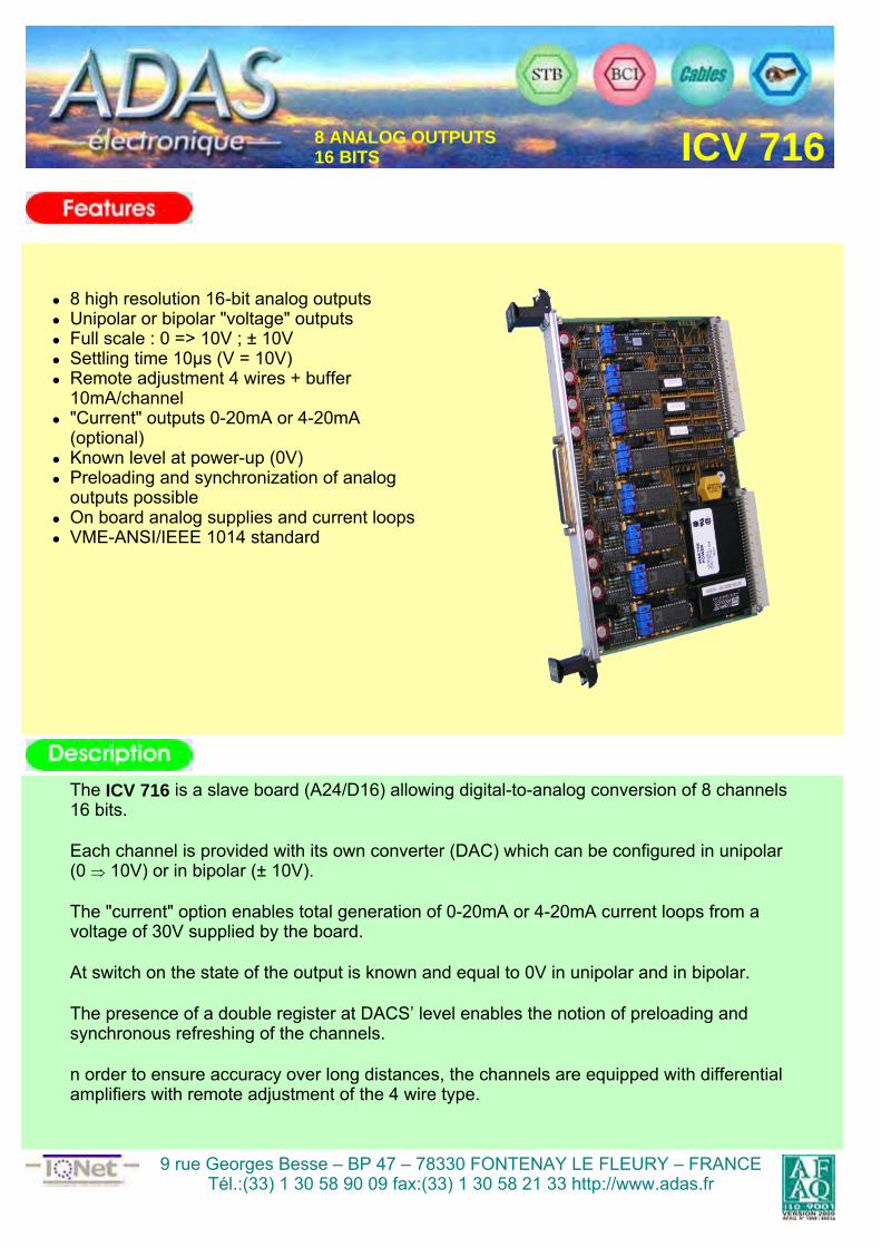
8 high resolution 16-bit analog outputsUnipolar or bipolar "voltage" outputsFull scale : 0 => 10V ; ± 10V Settling time 10µs (V = 10V)Remote adjustment 4 wires + buffer 10mA/channel"Current" outputs 0-20mA or 4-20mA (optional)Known level at power-up (0V)Preloading and synchronization of analog outputs possibleOn board analog supplies and current loops VME-ANSI/IEEE 1014 standard
The ICV 716 is a slave board (A24/D16) allowing digital-to-analog conversion of 8 channels 16 bits.
Each channel is provided with its own converter (DAC) which can be configured in unipolar(0 10V) or in bipolar (± 10V).
The "current" option enables total generation of 0-20mA or 4-20mA current loops from a voltage of 30V supplied by the board.
At switch on the state of the output is known and equal to 0V in unipolar and in bipolar.
The presence of a double register at DACS’ level enables the notion of preloading and synchronous refreshing of the channels.
n order to ensure accuracy over long distances, the channels are equipped with differential amplifiers with remote adjustment of the 4 wire type.
9 rue Georges Besse – BP 47 – 78330 FONTENAY LE FLEURY – FRANCE Tél.:(33) 1 30 58 90 09 fax:(33) 1 30 58 21 33 http://www.adas.fr
8 ANALOG OUTPUTS 16 BITS ICV 716
ICV 716
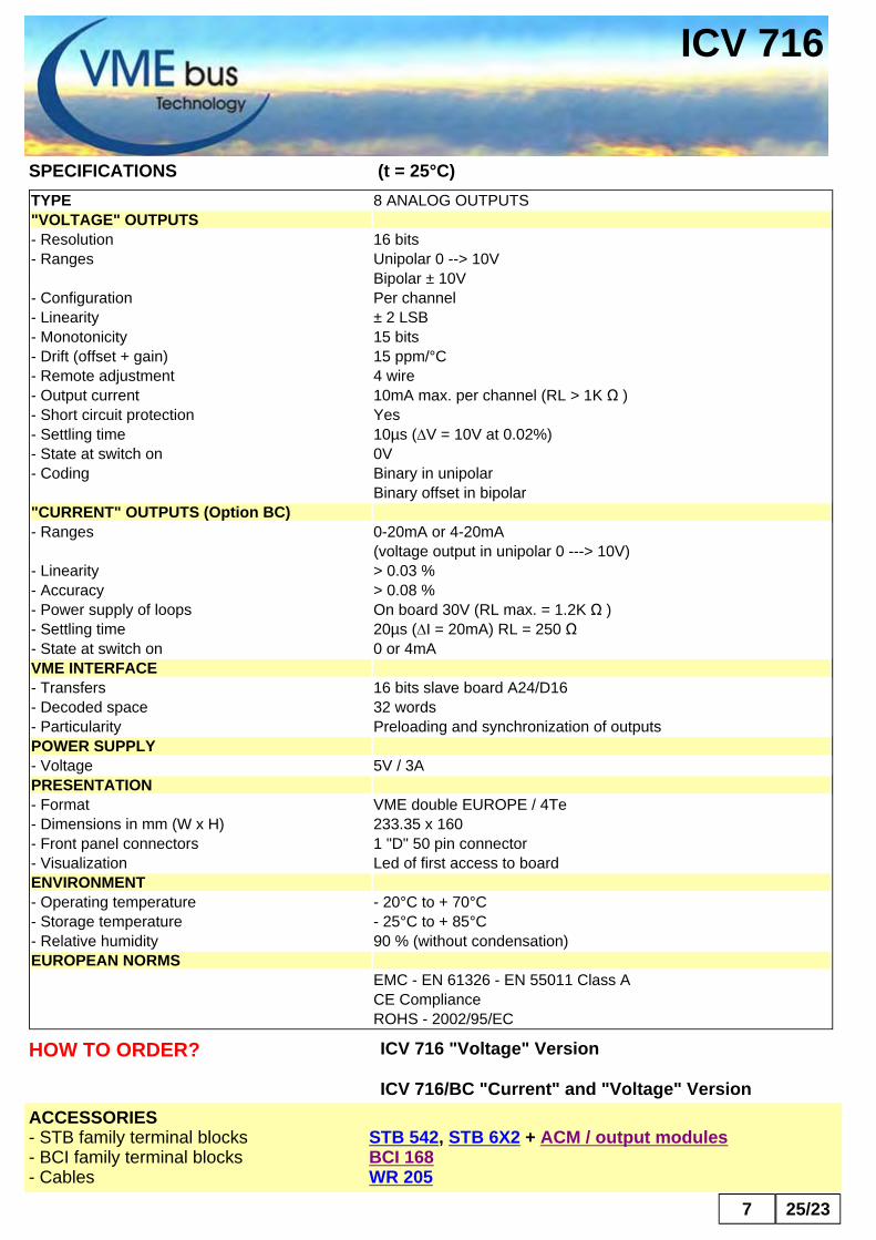
SPECIFICATIONS (t = 25°C)TYPE 8 ANALOG OUTPUTS "VOLTAGE" OUTPUTS- Resolution 16 bits- Ranges Unipolar 0 --> 10V
Bipolar ± 10V - Configuration Per channel - Linearity ± 2 LSB - Monotonicity 15 bits - Drift (offset + gain) 15 ppm/°C- Remote adjustment 4 wire- Output current 10mA max. per channel (RL > 1K Ω ) - Short circuit protection Yes- Settling time 10µs (∆V = 10V at 0.02%) - State at switch on 0V - Coding Binary in unipolar
Binary offset in bipolar "CURRENT" OUTPUTS (Option BC) - Ranges 0-20mA or 4-20mA
(voltage output in unipolar 0 ---> 10V) - Linearity > 0.03 % - Accuracy > 0.08 % - Power supply of loops On board 30V (RL max. = 1.2K Ω ) - Settling time 20µs (∆I = 20mA) RL = 250 Ω - State at switch on 0 or 4mA VME INTERFACE - Transfers 16 bits slave board A24/D16 - Decoded space 32 words - Particularity Preloading and synchronization of outputs POWER SUPPLY - Voltage 5V / 3A PRESENTATION- Format VME double EUROPE / 4Te - Dimensions in mm (W x H) 233.35 x 160 - Front panel connectors 1 "D" 50 pin connector - Visualization Led of first access to board ENVIRONMENT - Operating temperature - 20°C to + 70°C - Storage temperature - 25°C to + 85°C - Relative humidity 90 % (without condensation) EUROPEAN NORMS EMC - EN 61326 - EN 55011 Class A CE Compliance ROHS - 2002/95/EC
HOW TO ORDER? ICV 716 "Voltage" Version
ICV 716/BC "Current" and "Voltage" Version ACCESSORIES - STB family terminal blocks STB 542, STB 6X2 + ACM / output modules - BCI family terminal blocks BCI 168- Cables WR 205
7 25/23
ICV 716 – Rev. B – Edition 7 – 25/27
1
TRACEABILITY FORM
DOCUMENT FOLLOW-UP
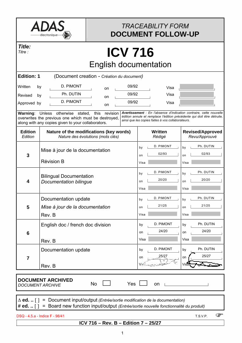
Title:Titre : ICV 716
English documentation
Edition: 1 (Document creation - Création du document)
Revised
Approved
Written
by
by
by D. PIMONT
Ph. DUTIN
D. PIMONT
on
on
on
09/92
09/92
09/92 Visa
Visa
Visa
Warning: Unless otherwise stated, this revision overwrites the previous one which must be destroyed, along with any copies given to your collaborators.
Avertissement : En l’absence d’indication contraire, cette nouvelle édition annule et remplace l’édition précédente qui doit être détruite, ainsi que les copies faites à vos collaborateurs.
EditionEdition
Nature of the modifications (key words) Nature des évolutions (mots clés)
WrittenRédigé
Revised/ApprovedRevu/Approuvé
3Mise à jour de la documentation
Révision B
on
Visa
by D. PIMONT
02/93 on
Visa
by Ph. DUTIN
02/93
4Bilingual Documentation Documentation bilingue on
Visa
by D. PIMONT
20/20 on
Visa
by Ph. DUTIN
20/20
5
Documentation update
Mise à jour de la documentation
Rev. B
on
Visa
by D. PIMONT
21/25 on
Visa
by Ph. DUTIN
21/25
6
English doc / french doc division
Rev. B
on
Visa
by
24/20
D. PIMONT
on
Visa
by
24/20
Ph. DUTIN
7
Documentation update
Rev. B
on
Visa
by
25/27
D. PIMONT
on
Visa
by
25/27
Ph. DUTIN
DOCUMENT ARCHIVEDDOCUMENT ARCHIVE No Yes on
ed. .. = Document input/output (Entrée/sortie modification de la documentation)
# ed. .. = Board new function input/output (Entrée/sortie nouvelle fonctionnalité du produit)
DSQ - 4.5.a - Indice F - 98/41 T.S.V.P.

ICV 716 – Rev. B – Edition 7 – 25/27
2
NOTES :
ICV 716 – Rev. B – Edition 7 – 25/27
3
ICV 716
SUMMARY
Chapter A Presentation.............................................4
A.1. Wiring and interconnection ..................................................................4
Chapter B Operation..................................................5
B.1. Memory space........................................................................................5
B.2. Register mapping ..................................................................................5
B.3. Unipolar or bipolar outputs ..................................................................7
B.3.1. Unipolar ......................................................................................7B.3.2. Bipolar.........................................................................................7
B.4. Remote regulation .................................................................................8
B.5. Current loops .......................................................................................10
Chapter C Implementation ......................................11
C.1. Installation............................................................................................11
C.2. VME interface.......................................................................................12
C.3. Output connector ................................................................................13
C.4. Addressing...........................................................................................14
C.5. Outputs configuration.........................................................................15
C.5.1. “Voltage” outputs ......................................................................15C.5.2. “Current” outputs.......................................................................15C.5.3. Remote regulation ....................................................................16
C.6. Settings ................................................................................................17
Chapter D ADAS coupling terminal block .............20
Appendix ...................................................................21
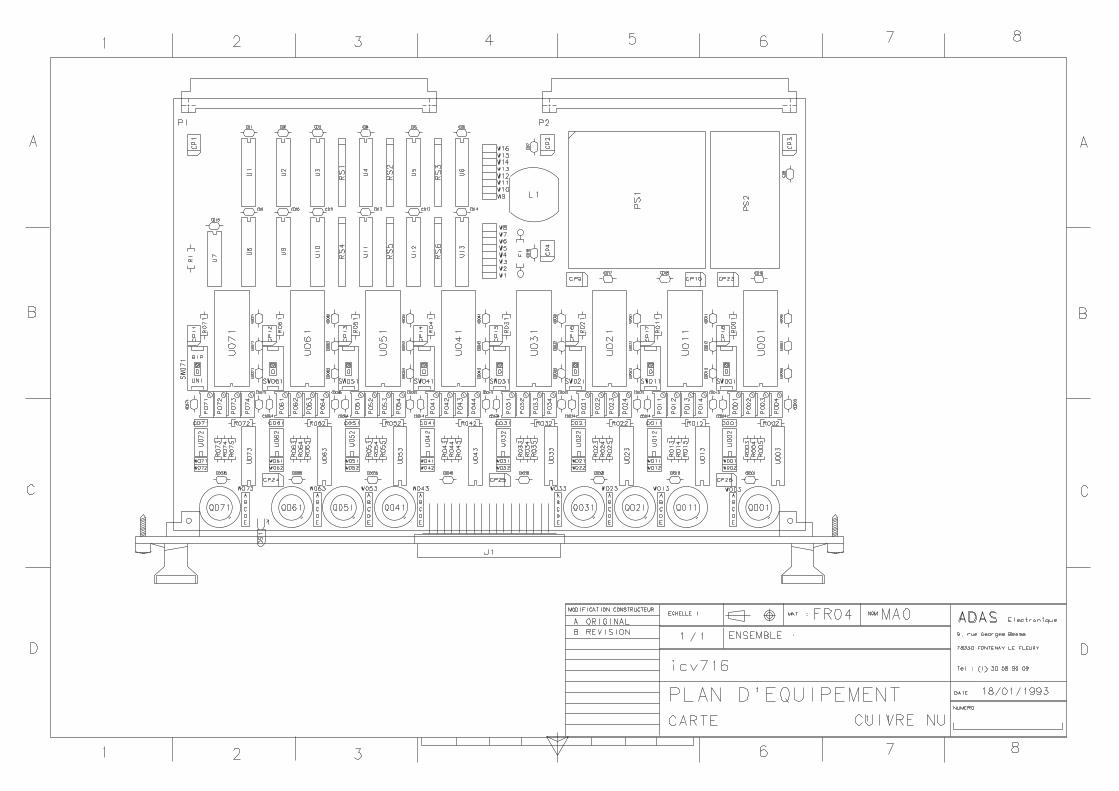
EQUIPMENT LAYOUT............................................................................................21
ICV 716 – Rev. B – Edition 7 – 25/27
4
Chapter A Presentation
The ICV 716 is a double Europe format VME board providing 8 analog 16-bit outputs.
The strong points of the product are:
Output configuration by channel,
status known at power-up,
remote regulation,
great precision and stability,
attractive cost.
A.1. Wiring and interconnection
If the reader wishes it, application examples of interconnections are given in the chapter Other Services "Wiring and Config" on our Web site.
ICV 716 – Rev. B – Edition 7 – 25/27
5
Chapter B Operation
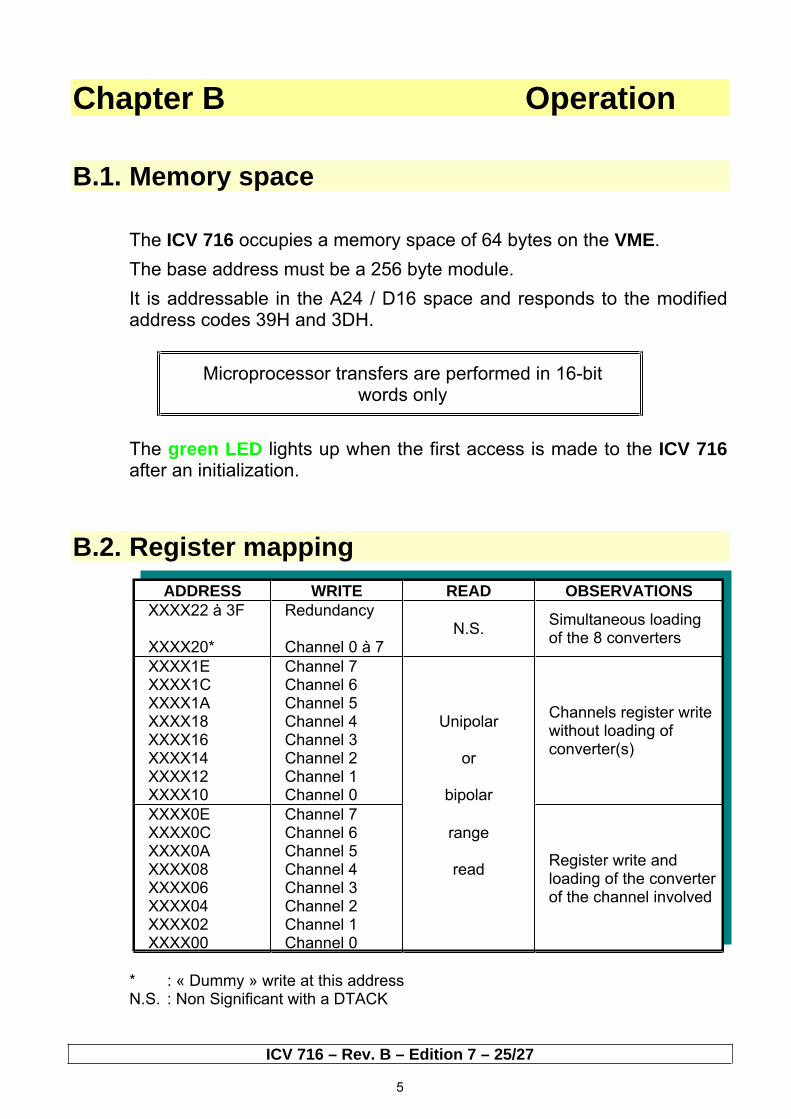
B.1. Memory space
The ICV 716 occupies a memory space of 64 bytes on the VME.
The base address must be a 256 byte module.
It is addressable in the A24 / D16 space and responds to the modified address codes 39H and 3DH.
Microprocessor transfers are performed in 16-bit words only
The green LED lights up when the first access is made to the ICV 716after an initialization.
B.2. Register mapping
ADDRESS WRITE READ OBSERVATIONS
XXXX22 à 3F
XXXX20*
Redundancy
Channel 0 à 7 N.S.
Simultaneous loading of the 8 converters
XXXX1EXXXX1CXXXX1AXXXX18XXXX16XXXX14XXXX12XXXX10
Channel 7 Channel 6 Channel 5 Channel 4 Channel 3 Channel 2 Channel 1 Channel 0
Unipolar
or
bipolar
Channels register write without loading of converter(s)
XXXX0EXXXX0CXXXX0AXXXX08XXXX06XXXX04XXXX02XXXX00
Channel 7 Channel 6 Channel 5 Channel 4 Channel 3 Channel 2 Channel 1 Channel 0
range
readRegister write and loading of the converter of the channel involved
* : « Dummy » write at this address N.S. : Non Significant with a DTACK
ICV 716 – Rev. B – Edition 7 – 25/27
6
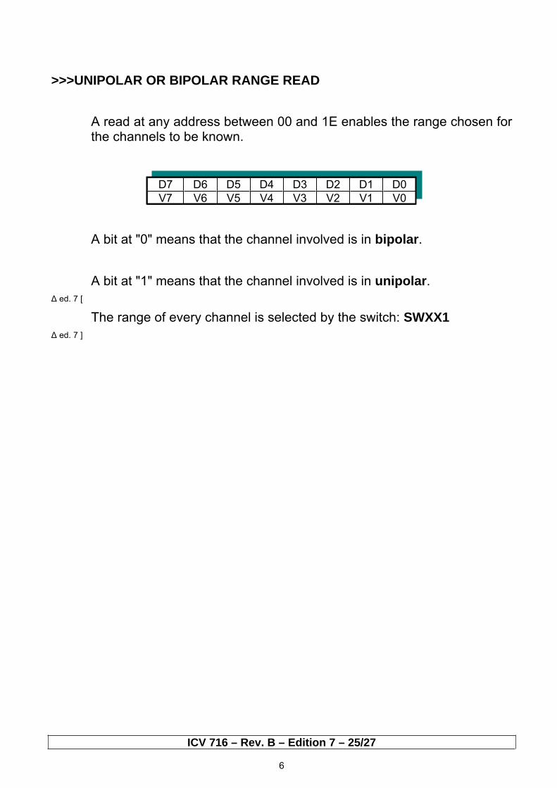
>>>UNIPOLAR OR BIPOLAR RANGE READ
A read at any address between 00 and 1E enables the range chosen for the channels to be known.
D7 D6 D5 D4 D3 D2 D1 D0
V7 V6 V5 V4 V3 V2 V1 V0
A bit at "0" means that the channel involved is in bipolar.
A bit at "1" means that the channel involved is in unipolar.
ed. 7 [
The range of every channel is selected by the switch: SWXX1
ed. 7 ]
ICV 716 – Rev. B – Edition 7 – 25/27
7
B.3. Unipolar or bipolar outputs
Each channel of the ICV 716 board can be configured in unipolar or
bipolar (SWXX1).
B.3.1. Unipolar
SWXX1 = Unipolar
Coding is in binary
FFFF = + 9,9998V
8000 = + 5,0000V
0000 = 0V
B.3.2. Bipolar
SWXX1 = Bipolar
Coding is in binary offset
FFFF = + 9,9996V
8000 = 0V
0000 = - 10V
>>>Note:
At power-up, the board has a voltage of 0V on output in both unipolar and bipolar.
XX = channel number from 0 to 7.
ICV 716 – Rev. B – Edition 7 – 25/27
8
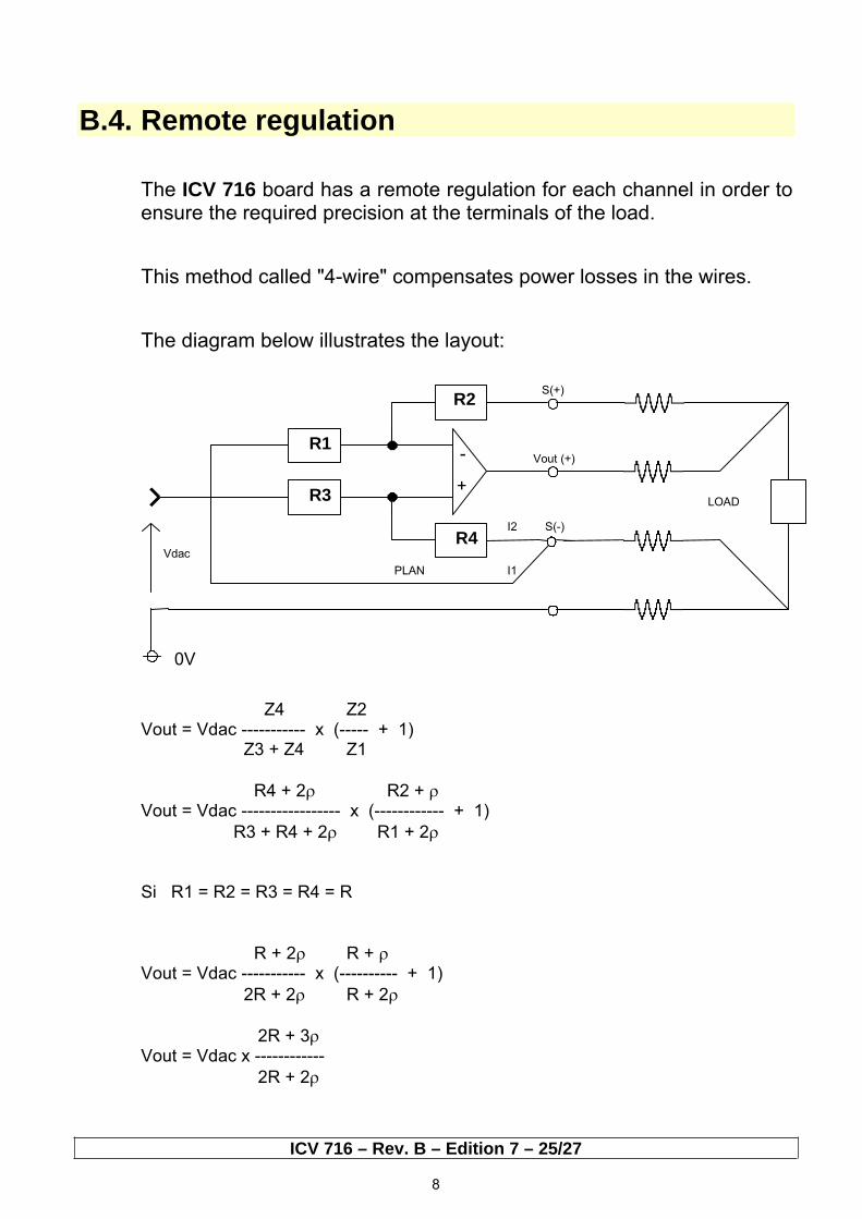
B.4. Remote regulation
The ICV 716 board has a remote regulation for each channel in order to ensure the required precision at the terminals of the load.
This method called "4-wire" compensates power losses in the wires.
The diagram below illustrates the layout:
R2
-
+
R1
VdacR4
R3
I1
I2 S(-)
Vout (+)
S(+)
0V
PLAN
LOAD
Z4 Z2 Vout = Vdac ----------- x (----- + 1) Z3 + Z4 Z1
R4 + 2 R2 + Vout = Vdac ----------------- x (------------ + 1)
R3 + R4 + 2 R1 + 2
Si R1 = R2 = R3 = R4 = R
R + 2 R + Vout = Vdac ----------- x (---------- + 1)
2R + 2 R + 2
2R + 3Vout = Vdac x ------------
2R + 2
ICV 716 – Rev. B – Edition 7 – 25/27
9
The example below illustrates the gain in precision of 4-wire regulation
Let: R load = 2K Iout = 5mA
= 1
in INA 105 R1 = R2 =R3 = R4 = 25K
a) With a remote regulation
The error is 1/50000ème
b) Without remote regulation
Vdac = Vout = (2 x Iout) + Vload
whence Vload = Vdac - 2 I
For 10V Vload = 9,990V
Let an error of 1/1000 (50 time greater).
>>>Notes:
x (Iload + I1 + I2) = VCM
This common mode voltage is inhibited by the instrumentatioin amplifier.
The term 2 comes from the fact that there is twice the same current (I1 = I2) flowing in the resistance of the wire taking the ground reference.
ICV 716 – Rev. B – Edition 7 – 25/27
10
B.5. Current loops
In the industrial world, current loops are often used. They enable several items of equipment to be wired in series and the principle is unaffected by line power losses.
The "BC" version of the ICV 716 therefore offers the possibility of 8 "current loop" outputs.
Conditioning of the loops is complete and does not require any external power supply.
A DC/DC converter on the board supplies + 30V.
The outputs are configurable by strap in two ranges :
0 20mA ou 4 20mA
It should be noted that the unipolar voltage output 0 10V compulsory in this case is also available on the voltage output.
ICV 716 – Rev. B – Edition 7 – 25/27
11
Chapter C Implementation
C.1. Installation
The user will beforehand read the on-line available for consultation document on our Internet site in the chapter Other Services "Implementing":
GENERAL INSTRUCTIONS FOR
IMPLEMENTING ADAS PRODUCTS INSTRUCTIONS GENERALES DE
MISE EN OEUVRE DES PRODUITS ADAS
The frame must be turned off before plugging in the product.
ICV 716 – Rev. B – Edition 7 – 25/27
12
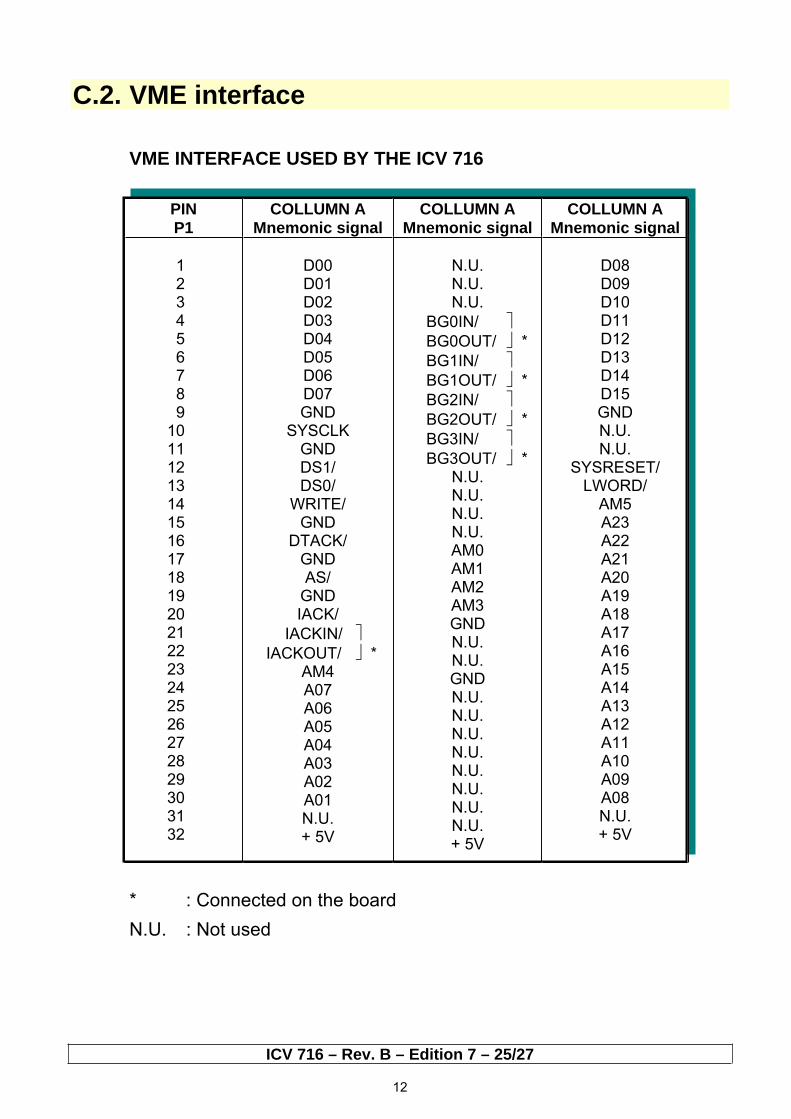
C.2. VME interface
VME INTERFACE USED BY THE ICV 716
PIN
P1
COLLUMN A
Mnemonic signal
COLLUMN A
Mnemonic signal
COLLUMN A
Mnemonic signal
1 2 3 4 5 6 7 8 9 10 11 12 13 14 15 16 17 18 19 20 21 22 23 24 25 26 27 28 29 30 31 32
D00D01D02D03D04D05D06D07GND
SYSCLKGNDDS1/DS0/
WRITE/GND
DTACK/GNDAS/
GNDIACK/
IACKIN/
IACKOUT/ * AM4A07A06A05A04A03A02A01N.U.+ 5V
N.U.N.U.N.U.
BG0IN/
BG0OUT/ *
BG1IN/
BG1OUT/ *
BG2IN/
BG2OUT/ *
BG3IN/
BG3OUT/ * N.U.N.U.N.U.N.U.AM0AM1AM2AM3GNDN.U.N.U.GNDN.U.N.U.N.U.N.U.N.U.N.U.N.U.N.U.+ 5V
D08D09D10D11D12D13D14D15GNDN.U.N.U.
SYSRESET/LWORD/
AM5A23A22A21A20A19A18A17A16A15A14A13A12A11A10A09A08N.U.+ 5V
* : Connected on the board
N.U. : Not used
ICV 716 – Rev. B – Edition 7 – 25/27
13
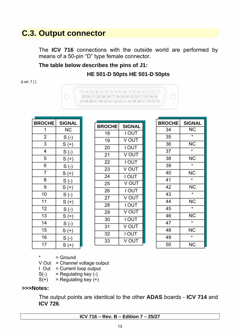
C.3. Output connector
The ICV 716 connections with the outside world are performed by means of a 50-pin “D” type female connector.
The table below describes the pins of J1:
HE 501-D 50pts HE 501-D 50pts
ed. 7 [ ]
BROCHE SIGNAL
1
2
3
4
5
6
7
8
9
10
11
12
13
14
15
16
17
SIGNAL
18
19
20
21
22
23
24
25
26
27
28
29
30
31
32
33
SIGNAL
34
35
36
37
38
39
40
41
42
43
44
45
46
47
48
49
50
BROCHEBROCHE
NC
S (-)
S (+)
S (-)
S (+)
S (-)
S (+)
S (-)
S (+)
S (-)
S (+)
S (-)
S (+)
S (-)
S (+)
S (-)
S (+)
I OUT
V OUT
I OUT
V OUT
I OUT
V OUT
I OUT
V OUT
I OUT
V OUT
I OUT
V OUT
I OUT
V OUT
I OUT
V OUT
NC
*
NC
*
NC
*
NC
*
NC
*
NC
*
NC
*
NC
*
NC
* = Ground V Out = Channel voltage output I Out = Current loop output S(-) = Regulating key (-) S(+) = Regulating key (+)
>>>Notes:
The output points are identical to the other ADAS boards - ICV 714 and
ICV 726.
ICV 716 – Rev. B – Edition 7 – 25/27
14
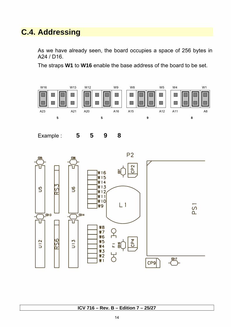
C.4. Addressing
As we have already seen, the board occupies a space of 256 bytes in A24 / D16.
The straps W1 to W16 enable the base address of the board to be set.
W16 W13 W12 W9 W8 W5 W4 W1
A23 A21 A20 A16 A15 A12 A11 A8
5 5 9 8
Example : 5 5 9 8
ICV 716 – Rev. B – Edition 7 – 25/27
15
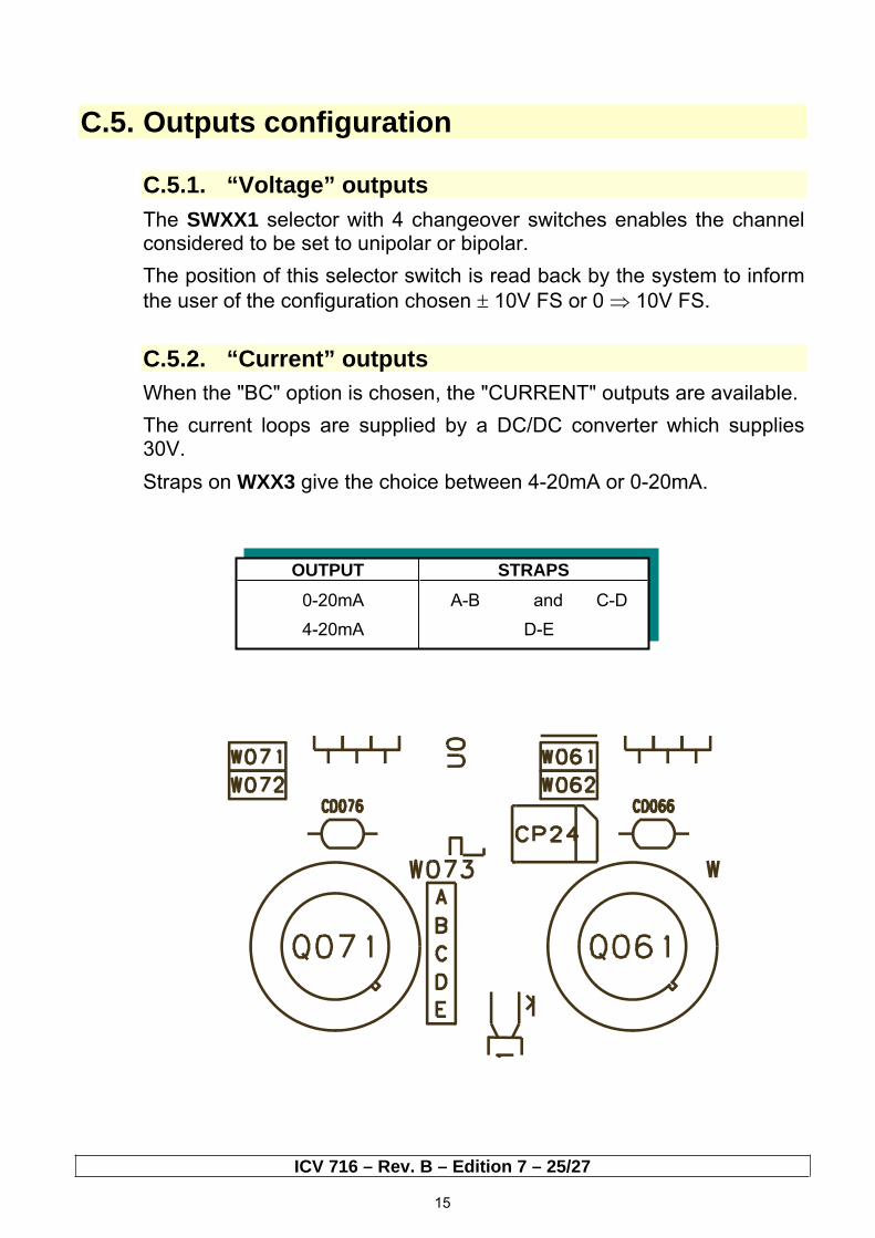
C.5. Outputs configuration
C.5.1. “Voltage” outputs
The SWXX1 selector with 4 changeover switches enables the channel considered to be set to unipolar or bipolar.
The position of this selector switch is read back by the system to inform
the user of the configuration chosen 10V FS or 0 10V FS.
C.5.2. “Current” outputs
When the "BC" option is chosen, the "CURRENT" outputs are available.
The current loops are supplied by a DC/DC converter which supplies 30V.
Straps on WXX3 give the choice between 4-20mA or 0-20mA.
OUTPUT STRAPS
0-20mA
4-20mA
A-B and C-D
D-E
ICV 716 – Rev. B – Edition 7 – 25/27
16
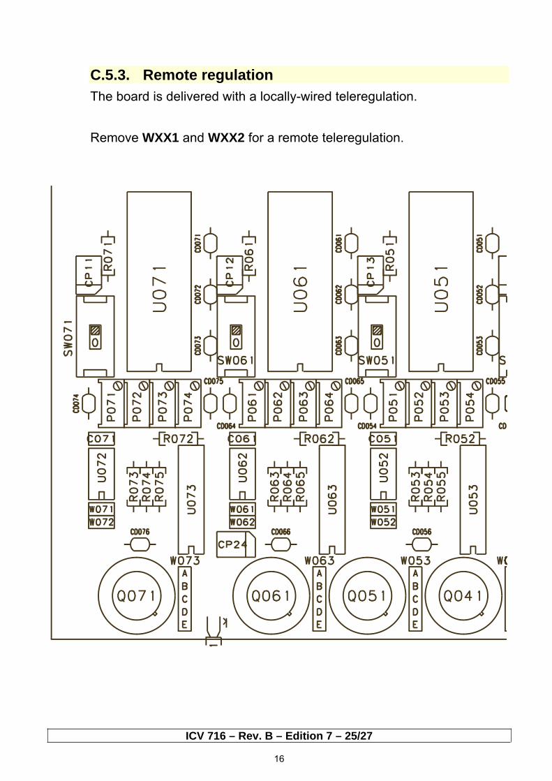
C.5.3. Remote regulation
The board is delivered with a locally-wired teleregulation.
Remove WXX1 and WXX2 for a remote teleregulation.
ICV 716 – Rev. B – Edition 7 – 25/27
17
C.6. Settings
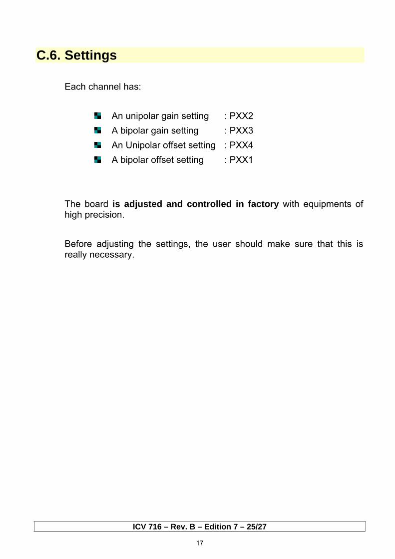
Each channel has:
An unipolar gain setting : PXX2
A bipolar gain setting : PXX3
An Unipolar offset setting : PXX4
A bipolar offset setting : PXX1
The board is adjusted and controlled in factory with equipments of high precision.
Before adjusting the settings, the user should make sure that this is really necessary.
ICV 716 – Rev. B – Edition 7 – 25/27
18
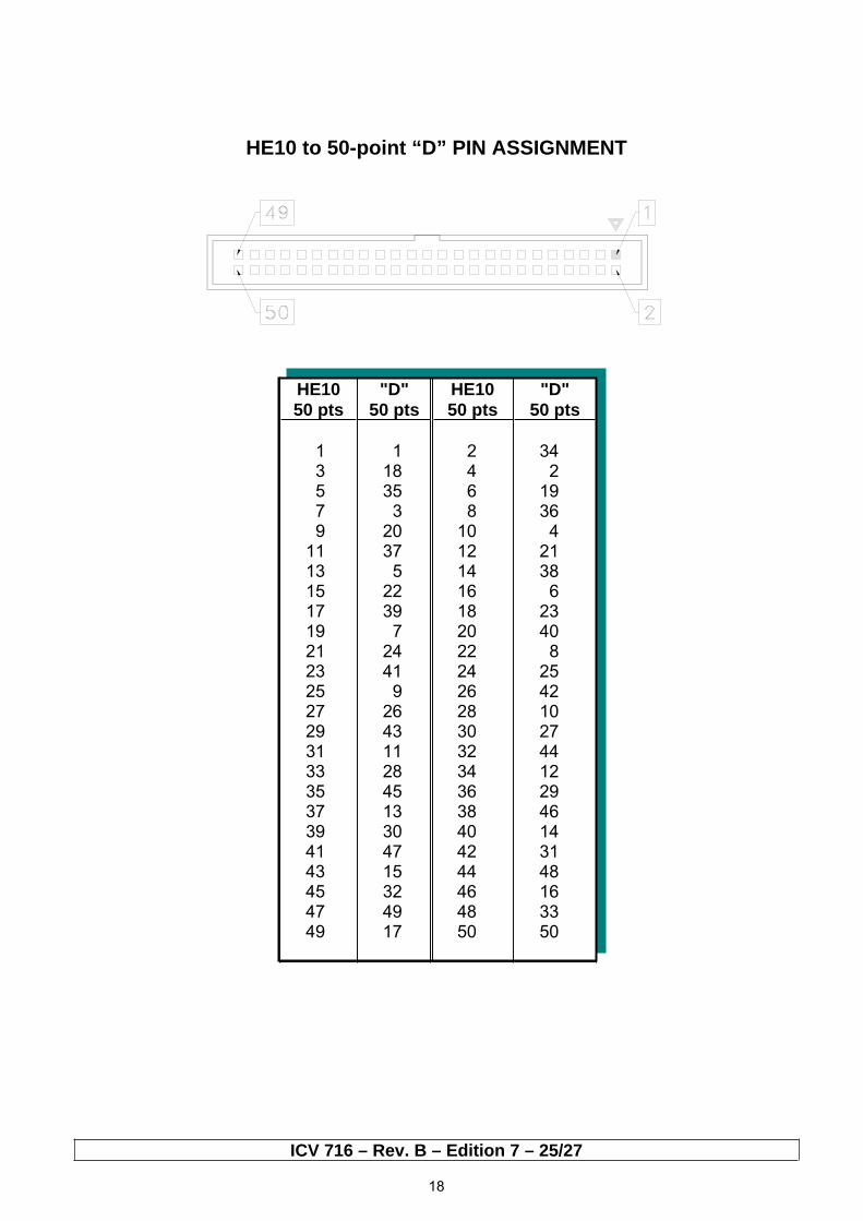
HE10 to 50-point “D” PIN ASSIGNMENT
HE10
50 pts
"D"
50 pts
HE10
50 pts
"D"
50 pts
1 3 5 7 9 1113151719212325272931333537394143454749
1 1835 3 2037 5 2239 7 2441 9 264311284513304715324917
2 4 6 8 101214161820222426283032343638404244464850
34 2 1936 4 2138 6 2340 8 2542102744122946143148163350
ICV 716 – Rev. B – Edition 7 – 25/27
19
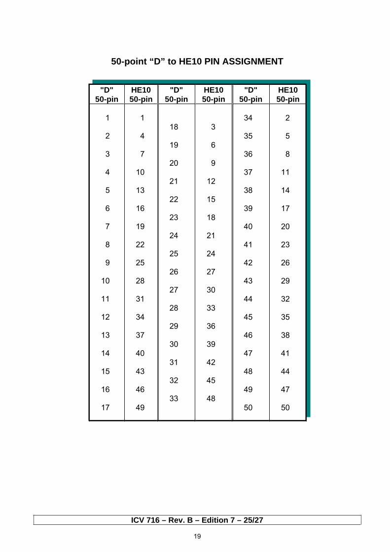
50-point “D” to HE10 PIN ASSIGNMENT
"D"
50-pin
HE10
50-pin
"D"
50-pin
HE10
50-pin
"D"
50-pin
HE10
50-pin
1
2
3
4
5
6
7
8
9
10
11
12
13
14
15
16
17
1
4
7
10
13
16
19
22
25
28
31
34
37
40
43
46
49
18
19
20
21
22
23
24
25
26
27
28
29
30
31
32
33
3
6
9
12
15
18
21
24
27
30
33
36
39
42
45
48
34
35
36
37
38
39
40
41
42
43
44
45
46
47
48
49
50
2
5
8
11
14
17
20
23
26
29
32
35
38
41
44
47
50
ICV 716 – Rev. B – Edition 7 – 25/27
20
Chapter D ADAS coupling terminal block ed. 7 [
The board ICV 716 can be directly connected with several types of terminal blocks:
STB 542 :
Cabling via a cable WR205/XXX
STB 6X2 + output modules ACM : Voltage outputs with galvanic isolation of channels
>>>NOTE:
Old generation terminal blocks (STB 568 ; STB 570 ; STB 572) can also be connected.
On-line documentation of these products on : www.adas.fr
ADAS can design and manufacture other coupling terminal blocks for
the ICV 716.
ed. 7 ]
ICV 716 – Rev. B – Edition 7 – 25/27
21
Appendix
EQUIPMENT LAYOUT