Embed Size (px)
Citation preview

8/11/2019 7. Design Methodology Part 1
http://slidepdf.com/reader/full/7-design-methodology-part-1 1/64
1
Designing Combinational
Logic CircuitsDISEDIAKAN OLEH: AZMAN BIN MAT HUSSIN
JABATAN KEJURUTERAAN ELEKTRIK
POLITEKNIK TUANKU SYED SIRAJUDDIN
8/11/2019 7. Design Methodology Part 1
http://slidepdf.com/reader/full/7-design-methodology-part-1 2/64
2
Combinational Sequential
Output = f ( In ) Output = f ( In, Previous In )
CombinationalLogic
Circuit
Out In
CombinationalLogic
Circuit
Out In
State

8/11/2019 7. Design Methodology Part 1
http://slidepdf.com/reader/full/7-design-methodology-part-1 3/64
3

8/11/2019 7. Design Methodology Part 1
http://slidepdf.com/reader/full/7-design-methodology-part-1 4/64
4

8/11/2019 7. Design Methodology Part 1
http://slidepdf.com/reader/full/7-design-methodology-part-1 5/64

8/11/2019 7. Design Methodology Part 1
http://slidepdf.com/reader/full/7-design-methodology-part-1 6/64
6
VDD
F(In1,In2,…InN)
In1In2
InN
In1In2
InN
PUN
PDN
PMOS only
NMOS only
PUN and PDN are dual logic networks

8/11/2019 7. Design Methodology Part 1
http://slidepdf.com/reader/full/7-design-methodology-part-1 7/647
Transistors can be thought as a switch controlled by its gate signal
NMOS switch closes when switch control input is high
X Y
A B
Y = X if A and B
X Y
A
B Y = X if A OR B
NMOS Transistors pass a “strong” 0 but a “weak” 1

8/11/2019 7. Design Methodology Part 1
http://slidepdf.com/reader/full/7-design-methodology-part-1 8/648
X Y
A B
Y = X if A AND B = A + B
X Y
A
B Y = X if A OR B = AB
PMOS Transistors pass a “strong” 1 but a “weak” 0
PMOS switch closes when switch control input is low

8/11/2019 7. Design Methodology Part 1
http://slidepdf.com/reader/full/7-design-methodology-part-1 9/64
8/11/2019 7. Design Methodology Part 1
http://slidepdf.com/reader/full/7-design-methodology-part-1 10/64
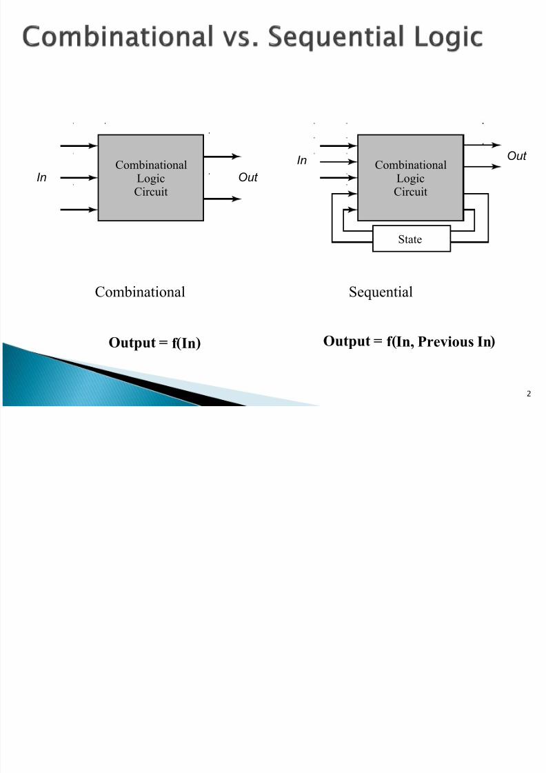
A stick diagram is a cartoon of a layout. Does show all components/vias (except
possibly tub ties), relative placement.
Does not show exact placement, transistor
sizes, wire lengths, wire widths, tubboundaries.

8/11/2019 7. Design Methodology Part 1
http://slidepdf.com/reader/full/7-design-methodology-part-1 11/64

8/11/2019 7. Design Methodology Part 1
http://slidepdf.com/reader/full/7-design-methodology-part-1 12/64
NMOS is formed when a polysilicon line is placed across an N-diffusion line.
PMOS is formed when a polysilicon line is placed across a
P-diffusion line.
Stick Diagram Rules

8/11/2019 7. Design Methodology Part 1
http://slidepdf.com/reader/full/7-design-methodology-part-1 13/64
No electrical connection happens when 2 different layerscrossing each other (e.g polysilicon crosses metal).
To connect 2 different layers (e.g. polysilicon and metal), acontact is placed on the crossing line with a black circle or X
sign.
Stick Diagram Rules

8/11/2019 7. Design Methodology Part 1
http://slidepdf.com/reader/full/7-design-methodology-part-1 14/64
Schematic Diagram Stick Diagram
VDD
GND
S D
S D
A
Y
8/11/2019 7. Design Methodology Part 1
http://slidepdf.com/reader/full/7-design-methodology-part-1 15/64
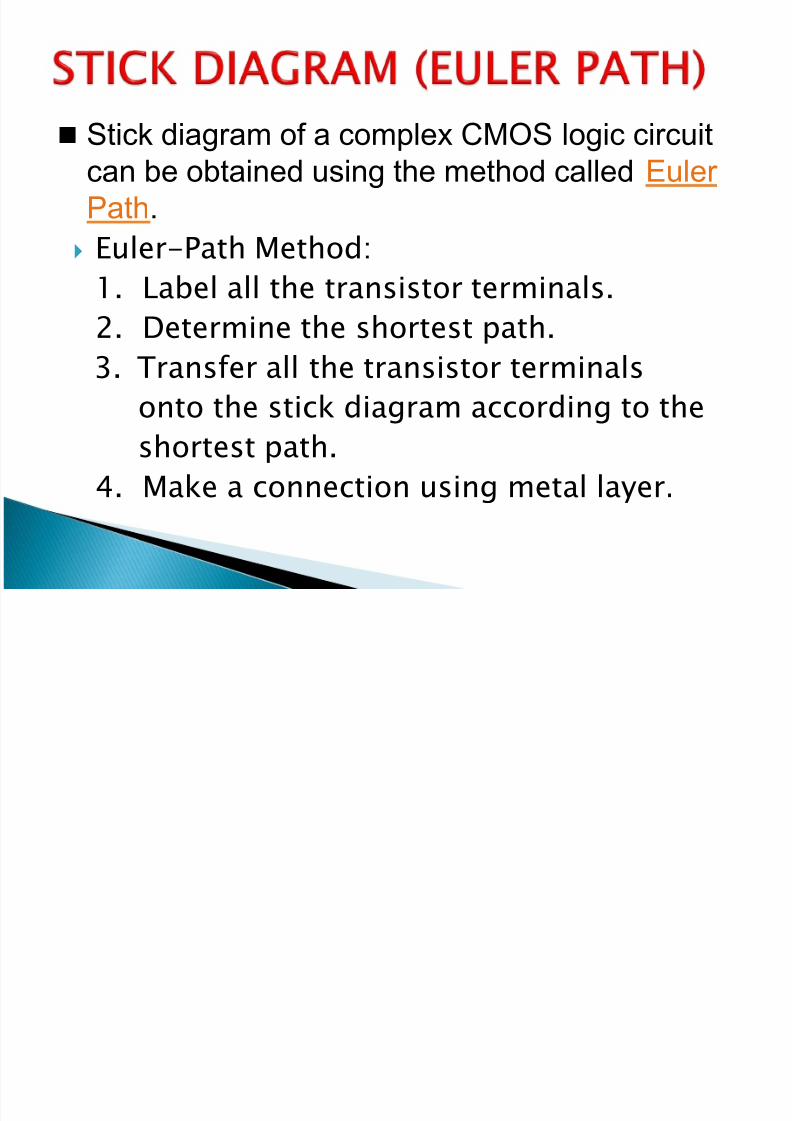
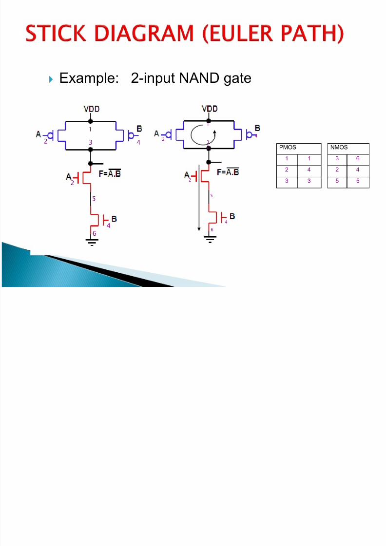
Stick diagram of a complex CMOS logic circuitcan be obtained using the method called Euler
Path.
Euler-Path Method:
1. Label all the transistor terminals.
2. Determine the shortest path.
3. Transfer all the transistor terminals
onto the stick diagram according to theshortest path.
4. Make a connection using metal layer.
8/11/2019 7. Design Methodology Part 1
http://slidepdf.com/reader/full/7-design-methodology-part-1 16/64
Example: 2-input NAND gate
1
2 3 4
2
4
5
6
1
2 32
4
2
4
5
6
PMOS
1 1
2 4
3 3
NMOS
3 6
2 4
5 5

8/11/2019 7. Design Methodology Part 1
http://slidepdf.com/reader/full/7-design-methodology-part-1 17/64
PMOS
1 1
2 4
3 3
NMOS
3 6
2 4
5 5
2 4 DD
GND A B
1 3 1
3 5 6
2 4 DD
GND A B
1 3 1
3 5 6
F
Example: 2-input NAND gate
8/11/2019 7. Design Methodology Part 1
http://slidepdf.com/reader/full/7-design-methodology-part-1 18/64
Transistors can be used as switches
g
s d
g = 0
s d
g = 1s d
0 strong 0
Input Output
1 degraded 1
g
s d
g = 0
s d
g = 1
s d
0 degraded 0
Input Output
strong 1
g = 1
g = 1
g = 0
g = 0
8/11/2019 7. Design Methodology Part 1
http://slidepdf.com/reader/full/7-design-methodology-part-1 19/64
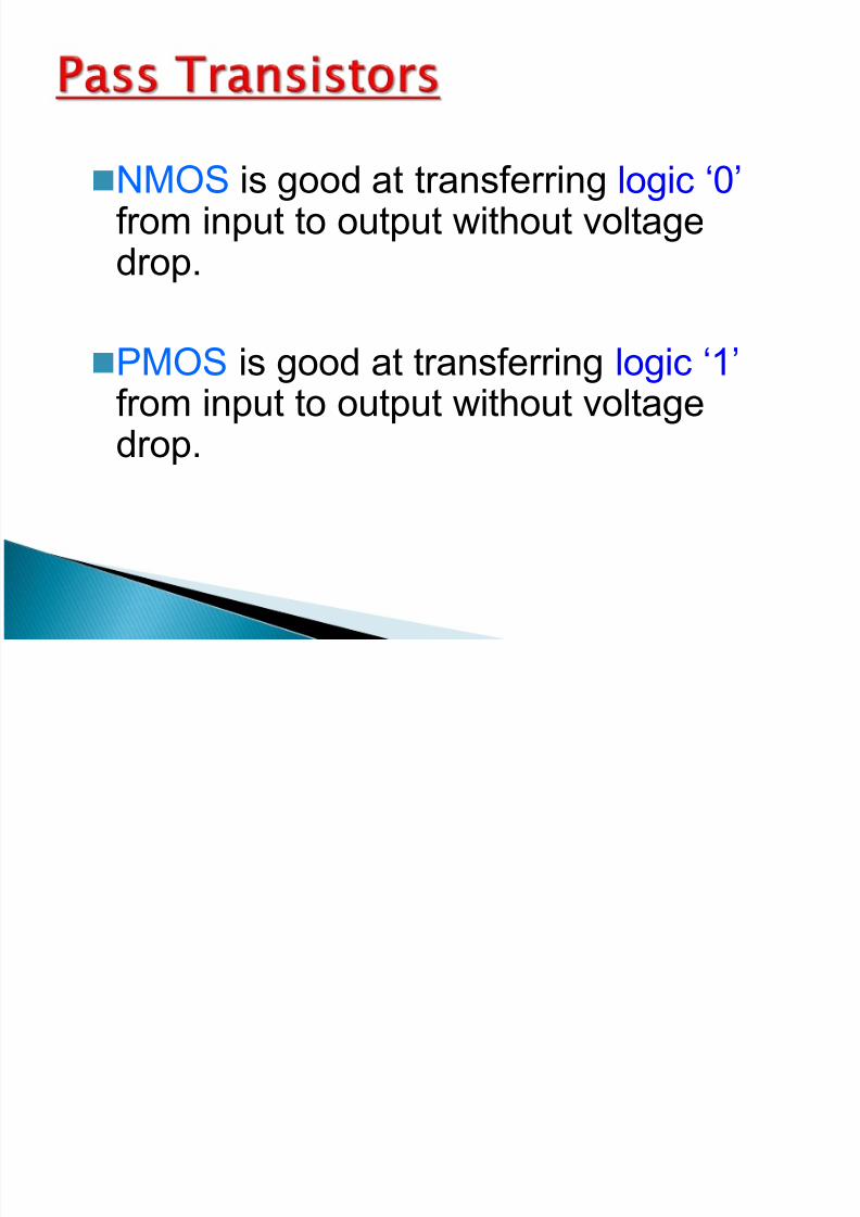
NMOS is good at transferring logic ‘0’from input to output without voltagedrop.
PMOS is good at transferring logic ‘1’from input to output without voltage
drop.

8/11/2019 7. Design Methodology Part 1
http://slidepdf.com/reader/full/7-design-methodology-part-1 20/64

8/11/2019 7. Design Methodology Part 1
http://slidepdf.com/reader/full/7-design-methodology-part-1 21/64
1. Clock pulse is supplied to NMOS transistor, and PMOS is given the invertedclock pulse.
2. If the clock pulse is low (logic ‘0’), both NMOS & PMOS transistor if OFF. No
data is transferred to the output.
3. If the clock pulse is high (logic ‘1’), both NMOS & PMOS transistor if ON. If the
input is logic ‘0’, NMOS will transfer the data to the output. If the input is logic
‘1’, PMOS will transfer the data to the output.
SYMBOL
SCHEMATIC LAYOUT
TRANSMISSION GATE

8/11/2019 7. Design Methodology Part 1
http://slidepdf.com/reader/full/7-design-methodology-part-1 22/64
22

8/11/2019 7. Design Methodology Part 1
http://slidepdf.com/reader/full/7-design-methodology-part-1 23/64
23
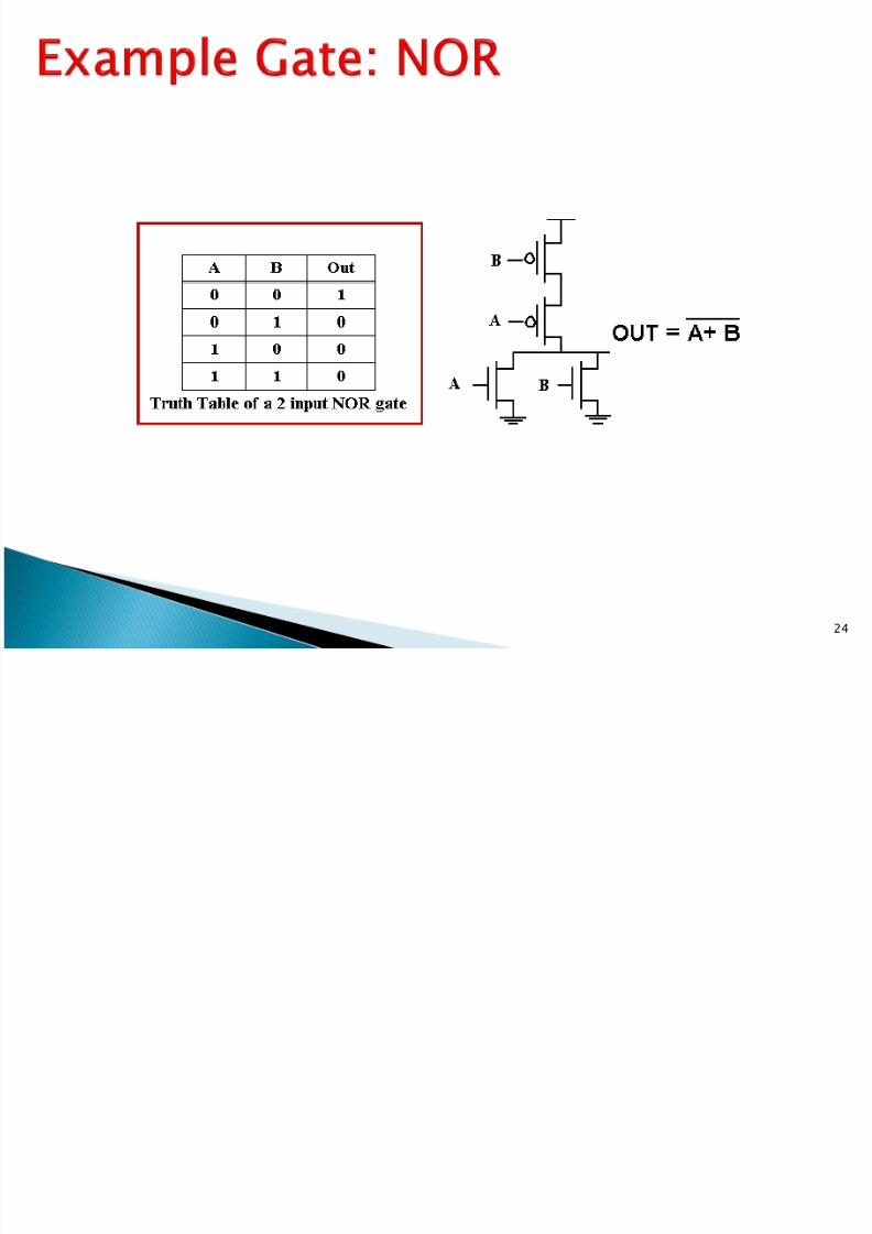
8/11/2019 7. Design Methodology Part 1
http://slidepdf.com/reader/full/7-design-methodology-part-1 24/64
24

8/11/2019 7. Design Methodology Part 1
http://slidepdf.com/reader/full/7-design-methodology-part-1 25/64
Standard Cells◦ General purpose logic◦ Can be synthesized◦ Same height, varying width
Datapath Cells◦ For regular, structured designs (arithmetic)◦ Includes some wiring in the cell◦ Fixed height and width
25

8/11/2019 7. Design Methodology Part 1
http://slidepdf.com/reader/full/7-design-methodology-part-1 26/64
26
signals
Routingchannel
VDD
GND

8/11/2019 7. Design Methodology Part 1
http://slidepdf.com/reader/full/7-design-methodology-part-1 27/64
27
M2
No Routingchannels
VDD
GNDM3
VDD
GND
Mirrored Cell
Mirrored Cell

8/11/2019 7. Design Methodology Part 1
http://slidepdf.com/reader/full/7-design-methodology-part-1 28/64
28
Cell boundary
N Well
Cell height 12 metal tracksMetal track is approx. 3 + 3 Pitch =repetitive distance between objects
Cell height is “12 pitch”
2
Rails ~10
In Out
V DD
GND

8/11/2019 7. Design Methodology Part 1
http://slidepdf.com/reader/full/7-design-methodology-part-1 29/64
29
In Out
V DD
GND
In Out
V DD
GND
With silicideddiffusion
With minimaldiffusionrouting
Out In
V DD
M 2
M 1

8/11/2019 7. Design Methodology Part 1
http://slidepdf.com/reader/full/7-design-methodology-part-1 30/64
30
A
Out
V DD
GND
B
2-input NAND gate
B
V DD
A

8/11/2019 7. Design Methodology Part 1
http://slidepdf.com/reader/full/7-design-methodology-part-1 31/64
31
High noise margins :
V OH and V OL are at V DD and GND , respectively.
No static power consumption : There never exists a direct path between V DD and
V SS ( GND ) in steady-state mode .
Comparable rise and fall times: (under appropriate sizing conditions)

8/11/2019 7. Design Methodology Part 1
http://slidepdf.com/reader/full/7-design-methodology-part-1 32/64
Full rail-to-rail swing; high noise margins Logic levels not dependent upon the relative
device sizes; ratioless Always a path to Vdd or Gnd in steady state;
low output impedance Extremely high input resistance; nearly zero
steady-state input current No direct path steady state between power
and ground; no static power dissipation Propagation delay function of load
capacitance and resistance of transistors
32

8/11/2019 7. Design Methodology Part 1
http://slidepdf.com/reader/full/7-design-methodology-part-1 33/64
33

8/11/2019 7. Design Methodology Part 1
http://slidepdf.com/reader/full/7-design-methodology-part-1 34/64
34
I n
p u t s
Switch
Network
Out Out
A
B
B
B
• N transistors
• No static consumption

8/11/2019 7. Design Methodology Part 1
http://slidepdf.com/reader/full/7-design-methodology-part-1 35/64
35
B
B
F = AB
0
8/11/2019 7. Design Methodology Part 1
http://slidepdf.com/reader/full/7-design-methodology-part-1 36/64
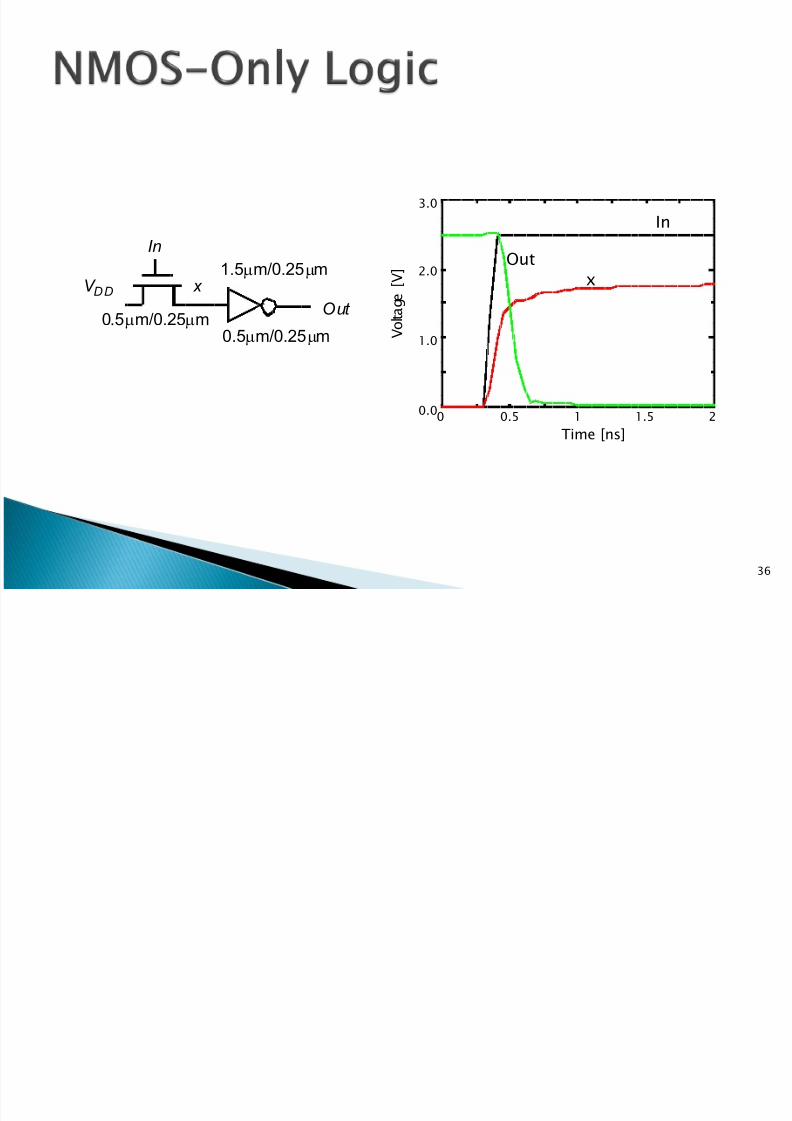
36
V DD
In
Out
x
0.5m/0.25m0.5m/0.25m
1.5m/0.25m
0 0.5 1 1.5 2 0.0
1.0
2.0
3.0
Time [ns]
V o
l t a g e [ V
]
x
Out
In

8/11/2019 7. Design Methodology Part 1
http://slidepdf.com/reader/full/7-design-methodology-part-1 37/64
37
A = 2.5 V
B
C = 2.5 V
C L
A = 2.5 V
C = 2.5 V
B
M 2
M 1
M n
Threshold voltage loss causes
static power consumption
V
B
does not pull up to 2.5V, but 2.5V -
TN
NMOS has higher threshold than PMOS (body effect)

8/11/2019 7. Design Methodology Part 1
http://slidepdf.com/reader/full/7-design-methodology-part-1 38/64
38
M 2
M 1
M n
M r
Out A
B
V DD
V DD Level Restorer
X
• Advantage: Full Swing
• Restorer adds capacitance, takes away pull down current at X
• Ratio problem

8/11/2019 7. Design Methodology Part 1
http://slidepdf.com/reader/full/7-design-methodology-part-1 39/64
39
0 100 200 300 400 500 0.0
1.0
2.0
W / L r =1.0/0.25 W / L
r =1.25/0.25
W / L r =1.50/0.25
W / L r =1.75/0.25
V
o l t a g e
[ V ]
Time [ps]
3.0 •Upper limit on restorer size•Pass-transistor pull-downcan have several transistors instack

8/11/2019 7. Design Methodology Part 1
http://slidepdf.com/reader/full/7-design-methodology-part-1 40/64
40
Out
V DD
V DD
2.5V
V DD
0V 2.5V
0V
WATCH OUT FOR LEAKAGE CURRENTS

8/11/2019 7. Design Methodology Part 1
http://slidepdf.com/reader/full/7-design-methodology-part-1 41/64
41
A
B
A
B
B B B B
A
B
A
B
F=AB
F=AB
F=A+B
F=A+B
B B
A
A
A
A
F=AÝ
F=AÝ
OR/NOR EXOR/NEXOR AND/NAND
F
F
Pass-Transistor
Network
Pass-Transistor
Network
AABB
AABB
Inverse
(a)
(b)

8/11/2019 7. Design Methodology Part 1
http://slidepdf.com/reader/full/7-design-methodology-part-1 42/64
42
A B
C
C
A B
C
C
B
C L
C = 0 V
A = 2.5 V
C = 2.5 V

8/11/2019 7. Design Methodology Part 1
http://slidepdf.com/reader/full/7-design-methodology-part-1 43/64
43
V out
0 V
2.5 V
2.5 VR n
R p
0.0 1.0 2.00
10
20
30
V out , V
essance,o
ms
R n
R p
R n || R p
8/11/2019 7. Design Methodology Part 1
http://slidepdf.com/reader/full/7-design-methodology-part-1 44/64
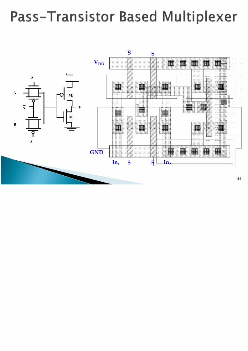
44
AM2
M1
B
S
S
S F
VDD
GND
VDD
In1 In
2 S S
S S

8/11/2019 7. Design Methodology Part 1
http://slidepdf.com/reader/full/7-design-methodology-part-1 45/64
45
A
B
F
B
A
B
B
M1
M2
M3/M4
8/11/2019 7. Design Methodology Part 1
http://slidepdf.com/reader/full/7-design-methodology-part-1 46/64
46
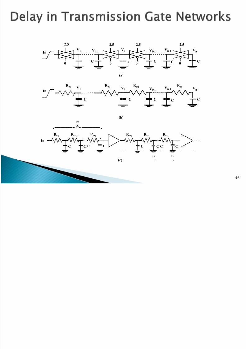
V 1 V i-1
C
2.5 2.5
0 0
V i V i+1
C C
2.5
0
V n-1 V n
C C
2.5
0
In
V 1 V i V i+1
C
V n-1 V n
C C
In
R eq R eq R eq R eq
C C
(a)
(b)
C
R eq R eq
C C
R eq
C C
R eq R eq
C C
R eq
C
In
m
(c)

8/11/2019 7. Design Methodology Part 1
http://slidepdf.com/reader/full/7-design-methodology-part-1 47/64
47

8/11/2019 7. Design Methodology Part 1
http://slidepdf.com/reader/full/7-design-methodology-part-1 48/64
48

8/11/2019 7. Design Methodology Part 1
http://slidepdf.com/reader/full/7-design-methodology-part-1 49/64
In static circuits at every point in time(except when switching) the output isconnected to either GND or VDD via a lowresistance path.◦ fan-in of n requires 2n (n N-type + n P-type)
devices
Dynamic circuits rely on the temporarystorage of signal values on the capacitance
of high impedance nodes.◦ requires on n + 2 (n +1 N-type + 1 P-type)transistors
49

8/11/2019 7. Design Methodology Part 1
http://slidepdf.com/reader/full/7-design-methodology-part-1 50/64
51
In1
In2 PDN
In3
Me
Mp
Clk
Clk
Out
CL
Out
Clk
Clk
A
B
C
Mp
Me
Two phase operationPrecharge (Clk = 0)Evaluate (Clk = 1)
on
off
1
off
on
((AB)+C)

8/11/2019 7. Design Methodology Part 1
http://slidepdf.com/reader/full/7-design-methodology-part-1 51/64
Once the output of a dynamic gate isdischarged, it cannot be charged again untilthe next precharge operation.
Inputs to the gate can make at most one
transition during evaluation.
Output can be in the high impedance stateduring and after evaluation (PDN off), state
is stored on CL
52
8/11/2019 7. Design Methodology Part 1
http://slidepdf.com/reader/full/7-design-methodology-part-1 52/64
Logic function is implemented by the PDNonly◦ number of transistors is N + 2 (versus 2N for static
complementary CMOS)
Full swing outputs (VOL = GND and VOH = VDD) Non-ratioed - sizing of the devices does not
affect the logic levels
Faster switching speeds◦ reduced load capacitance due to lower input capacitance (Cin)
◦ reduced load capacitance due to smaller output loading (Cout)
◦ no Isc, so all the current provided by PDN goes intodischarging CL
53

8/11/2019 7. Design Methodology Part 1
http://slidepdf.com/reader/full/7-design-methodology-part-1 53/64
Overall power dissipation usually higher thanstatic CMOS◦ no static current path ever exists between VDD and
GND (including Psc)◦
no glitching◦ higher transition probabilities◦ extra load on Clk
PDN starts to work as soon as the input
signals exceed VTn, so VM, VIH and VIL equal toVTn ◦ low noise margin (NML)
Needs a precharge/evaluate clock
54

8/11/2019 7. Design Methodology Part 1
http://slidepdf.com/reader/full/7-design-methodology-part-1 54/64
55
CL
Clk
Clk
Out
A
Mp
Me
Leakage sources
CLK
VOut
Precharge
Evaluate
Dominant component is subthreshold current

8/11/2019 7. Design Methodology Part 1
http://slidepdf.com/reader/full/7-design-methodology-part-1 55/64
56
CL
Clk
Clk
Me
Mp
A
B
Out
Mkp
Same approach as level restorer for pass-transistor logic
Keeper

8/11/2019 7. Design Methodology Part 1
http://slidepdf.com/reader/full/7-design-methodology-part-1 56/64
57
CL
Clk
Clk
CA
CB
B=0
A
Out
Mp
Me
Charge stored originally on CL isredistributed (shared) over CL andCA leading to reduced robustness

8/11/2019 7. Design Methodology Part 1
http://slidepdf.com/reader/full/7-design-methodology-part-1 57/64
58
CL=50fF
Clk
Clk
A A
B B B !B
C C
Out
Ca=15fF
Cc=15fF
Cb=15fF
Cd=10fF

8/11/2019 7. Design Methodology Part 1
http://slidepdf.com/reader/full/7-design-methodology-part-1 58/64
59
CL
VDD
CL
Vout
t Ca
VDD
VTn
VX – +=
or
Vout Vout t VDD –
CaC
L-------- VDD VTn VX – – = =
Vout
VDD
Ca
Ca C
L+
----------------------
– =
case 1) if V ou t
< V Tn
case 2) if V ou t
> V Tn
B = 0
Clk
X
C L
C a
C b
A
Out
M p
M a
V DD
M b
Clk M e

8/11/2019 7. Design Methodology Part 1
http://slidepdf.com/reader/full/7-design-methodology-part-1 59/64
60
Clk
Clk
Me
Mp
A
B
Out
MkpClk
Precharge internal nodes using a clock-driven transistor (at the costof increased area and power)

8/11/2019 7. Design Methodology Part 1
http://slidepdf.com/reader/full/7-design-methodology-part-1 60/64
61
CL1
Clk
Clk
B=0
A=0
Out1 Mp
Me
Out2
CL2 In
Dynamic NAND Static NAND
=1 =0

8/11/2019 7. Design Methodology Part 1
http://slidepdf.com/reader/full/7-design-methodology-part-1 61/64
-1
0
1
2
3
0 2 4 6
62
Time, ns
Clk
In
Out1
Out2

8/11/2019 7. Design Methodology Part 1
http://slidepdf.com/reader/full/7-design-methodology-part-1 62/64
63
CL
Clk
Clk
B
A
Out
Mp
Me
Coupling between Out and Clkinput of the precharge device dueto the gate to drain capacitance.So voltage of Out can rise above
VDD. The fast rising (and fallingedges) of the clock couple to Out.

8/11/2019 7. Design Methodology Part 1
http://slidepdf.com/reader/full/7-design-methodology-part-1 63/64
64
-0.5
0.5
1.5
2.5
0 0.5 1
Clk
Clk
In1
In2
In3
In4
Out
In &Clk
Out
Time, ns
Clock feedthrough
Clock feedthrough

8/11/2019 7. Design Methodology Part 1
http://slidepdf.com/reader/full/7-design-methodology-part-1 64/64
Capacitive coupling Substrate coupling
Minority charge injection
Supply noise (ground bounce)