Embed Size (px)
Citation preview
4-Bit Counter
Shanthan Mudhasani, ECE 533, University of Tennessee, Knoxville
Abstract—This paper presents a report on the design of a 4-bit Up Counter using J-K flip-
flop that has a clocked input with Reset. Performing simulations of various output parameters including rise time, fall time, highlights the performance of the designed counter in Cadence.
INTRODUCTION: The project aims to design a 4-bit counter using a Flip Flop. The design is done using cadence and AMI C5N 0.6 µm Technology library. A JK-Flip Flop was used to design the counter.
DESIGN JUSTIFICATION A. Counter Design Justification
• A 4-bit has 16 states counting from 0 to 15.This means that to design a 4-bit counter we need 4 Flip Flops.
• The counter also has a reset pin that enables it to enter an all-zero state i.e. the output of the counter is '0' if the reset is '1' irrespective of the clock and the current state of the flip flops.
• The counter also has CLA (carry look ahead) out pin that stores the carry. The CLA pin can be used to modify the design. For example the counter can be upgraded to a 8-bit counter by adding an other 4-bit adder to the CLA output.
• The outputs of the counter are named F0, F1, F2, and F3. These outputs also represent current state of the flip-flops.
B. Choice of Flip-Flop • The counter designed has 4 JK-Flip Flops. The JK-Flip Flop triggers at every
negative going edge of the clock signal. • A latch is a level-sensitive device. The major problem with latch-sensitive devices
is that during the same level of the clock signal, a race around condition might occur thereby making the device prone to glitches. This is avoided using the edge-sensitive J-K flip-flop.
• Also, the rising/falling edge has to be very sharp. Hence a 1 ns delay is specified for the clock signal transition from one state to the other.
• JK-Flip Flop is versatile. A reset can be easily implemented using the set-reset mode of the JK Flip-Flop. And a D or a T Flip Flop can be easily implemented using a JK-Flip Flop.
• The aspect ratio (W/L) of PMOS and NMOS transistors is taken to be (6µ/600n) and (3µ/600n) respectively. The width of the PMOS transistor has been
approximately be set to 6µm, for the same gate lengths, to account for the slow hole mobility compared to the electron mobility.
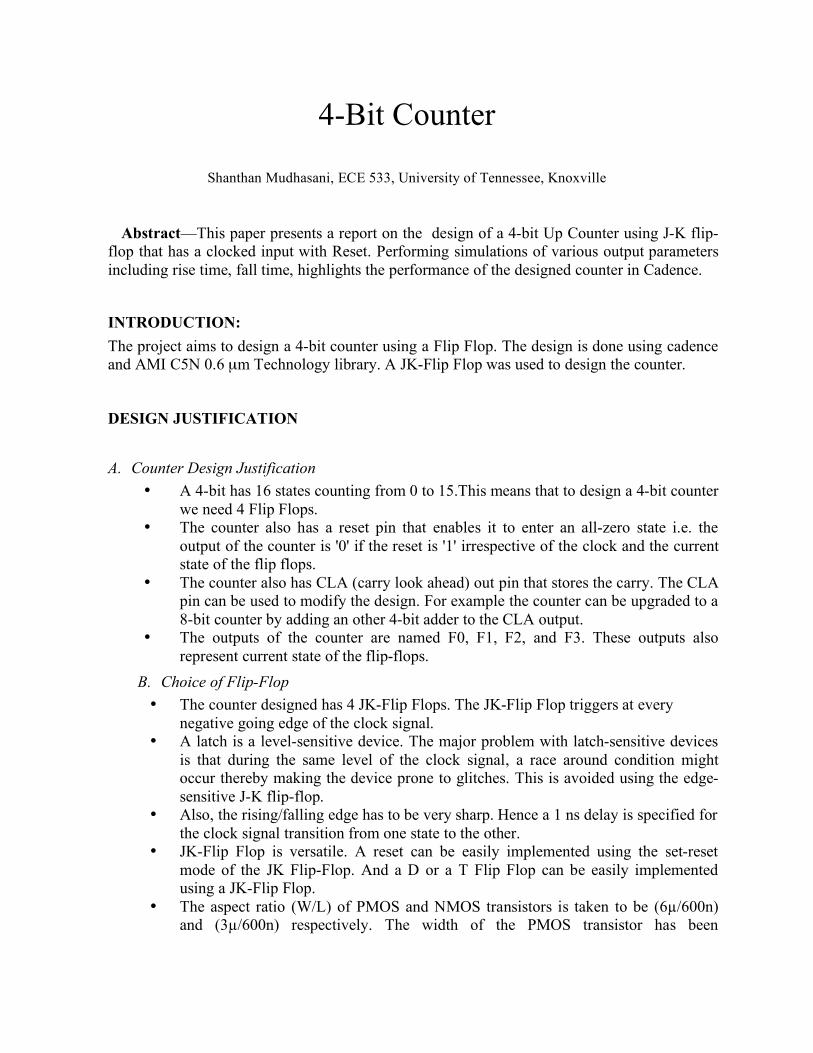
J-K FLIP-FLOP DESIGN A J-K flip-flop in the Master-slave configuration was used to implement the 4-bit up counter. As seen from the schematic of the J-K flip-flop in fig.1, two 3-input NAND gates, six 2-input NAND gates and two inverters in a feedback loop. A change of state may occur when the flip-flop senses a negative edge of the clock signal. Also, a reset pin is incorporated by the inclusion of an inverter, AND and OR gate. The reset pin operates on active high logic, i.e. the output Q is forced to ‘0’ irrespective of the input levels at J and K. Table 1 shows the truth table of the J-K flip-flop with Reset. The schematic was laid out using Composer Schematic
Fig.1
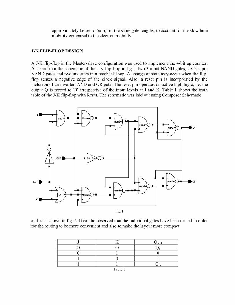
and is as shown in fig. 2. It can be observed that the individual gates have been turned in order for the routing to be more convenient and also to make the layout more compact.
J K Qn+1 O O Qn 0 1 0 1 0 1 1 1 Q'n
Table 1
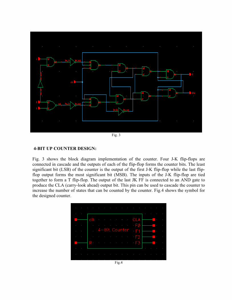
Fig. 3
4-BIT UP COUNTER DESIGN:
Fig. 3 shows the block diagram implementation of the counter. Four J-K flip-flops are connected in cascade and the outputs of each of the flip-flop forms the counter bits. The least significant bit (LSB) of the counter is the output of the first J-K flip-flop while the last flip-flop output forms the most significant bit (MSB). The inputs of the J-K flip-flop are tied together to form a T flip-flop. The output of the last JK FF is connected to an AND gate to produce the CLA (carry-look ahead) output bit. This pin can be used to cascade the counter to increase the number of states that can be counted by the counter. Fig.4 shows the symbol for the designed counter.
Fig.4
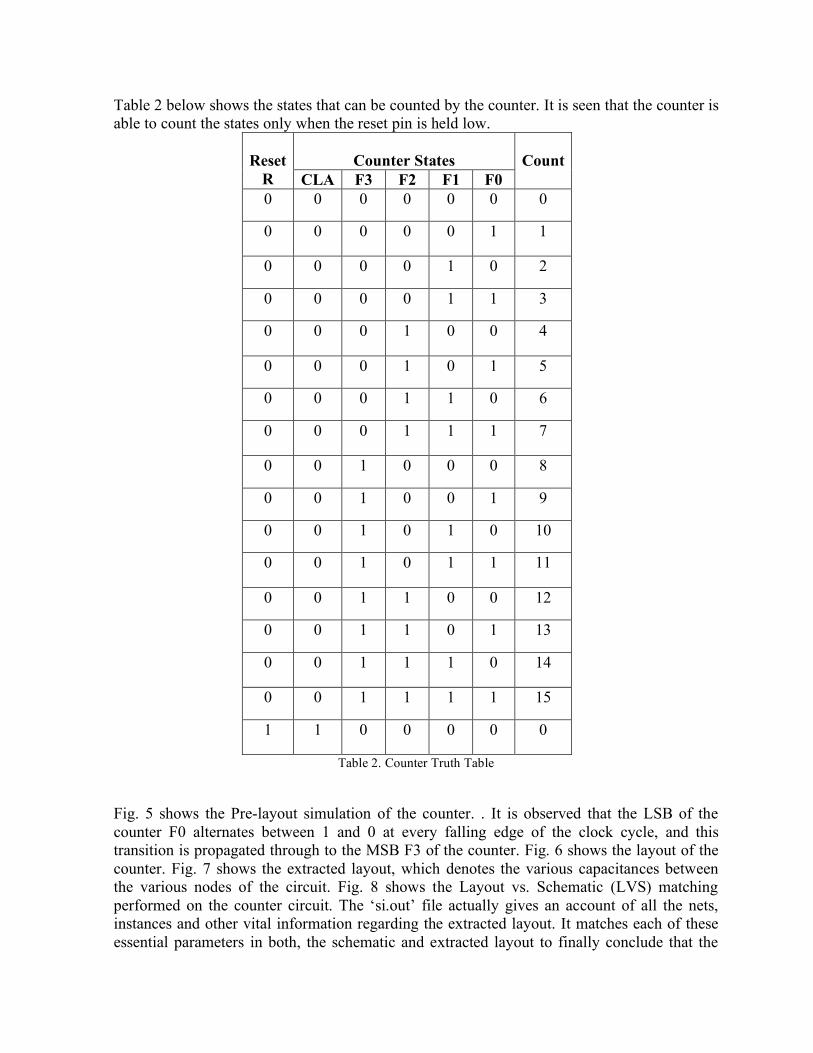
Table 2 below shows the states that can be counted by the counter. It is seen that the counter is able to count the states only when the reset pin is held low.
Counter States
Reset
R CLA F3 F2 F1 F0
Count
0 0 0 0 0 0 0
0 0 0 0 0 1 1
0 0 0 0 1 0 2
0 0 0 0 1 1 3
0 0 0 1 0 0 4
0 0 0 1 0 1 5
0 0 0 1 1 0 6
0 0 0 1 1 1 7
0 0 1 0 0 0 8
0 0 1 0 0 1 9
0 0 1 0 1 0 10
0 0 1 0 1 1 11
0 0 1 1 0 0 12
0 0 1 1 0 1 13
0 0 1 1 1 0 14
0 0 1 1 1 1 15
1 1 0 0 0 0 0
Table 2. Counter Truth Table
Fig. 5 shows the Pre-layout simulation of the counter. . It is observed that the LSB of the counter F0 alternates between 1 and 0 at every falling edge of the clock cycle, and this transition is propagated through to the MSB F3 of the counter. Fig. 6 shows the layout of the counter. Fig. 7 shows the extracted layout, which denotes the various capacitances between the various nodes of the circuit. Fig. 8 shows the Layout vs. Schematic (LVS) matching performed on the counter circuit. The ‘si.out’ file actually gives an account of all the nets, instances and other vital information regarding the extracted layout. It matches each of these essential parameters in both, the schematic and extracted layout to finally conclude that the
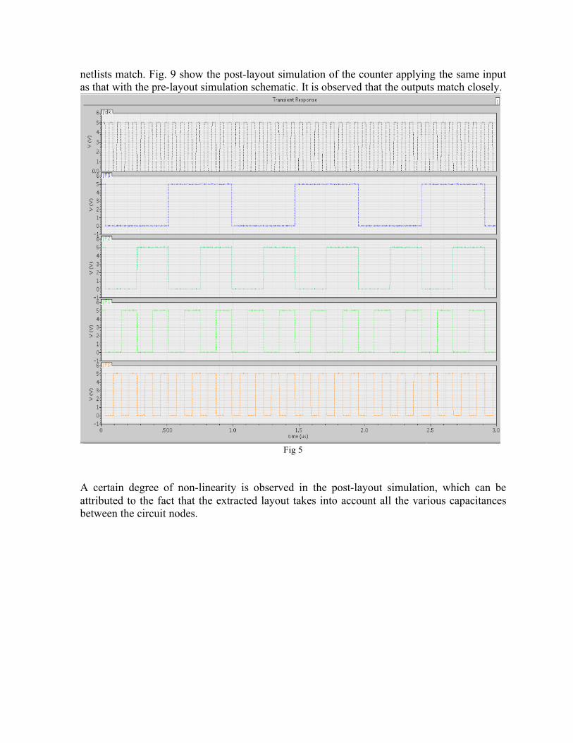
netlists match. Fig. 9 show the post-layout simulation of the counter applying the same input as that with the pre-layout simulation schematic. It is observed that the outputs match closely.
Fig 5
A certain degree of non-linearity is observed in the post-layout simulation, which can be attributed to the fact that the extracted layout takes into account all the various capacitances between the circuit nodes.
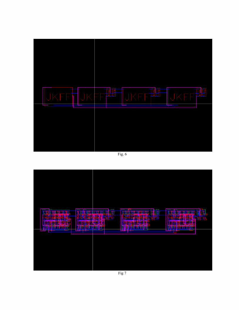
Fig. 6
Fig 7
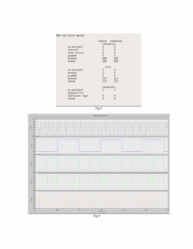
Fig 8
Fig 9
PERFORMANCE PARAMETERS:
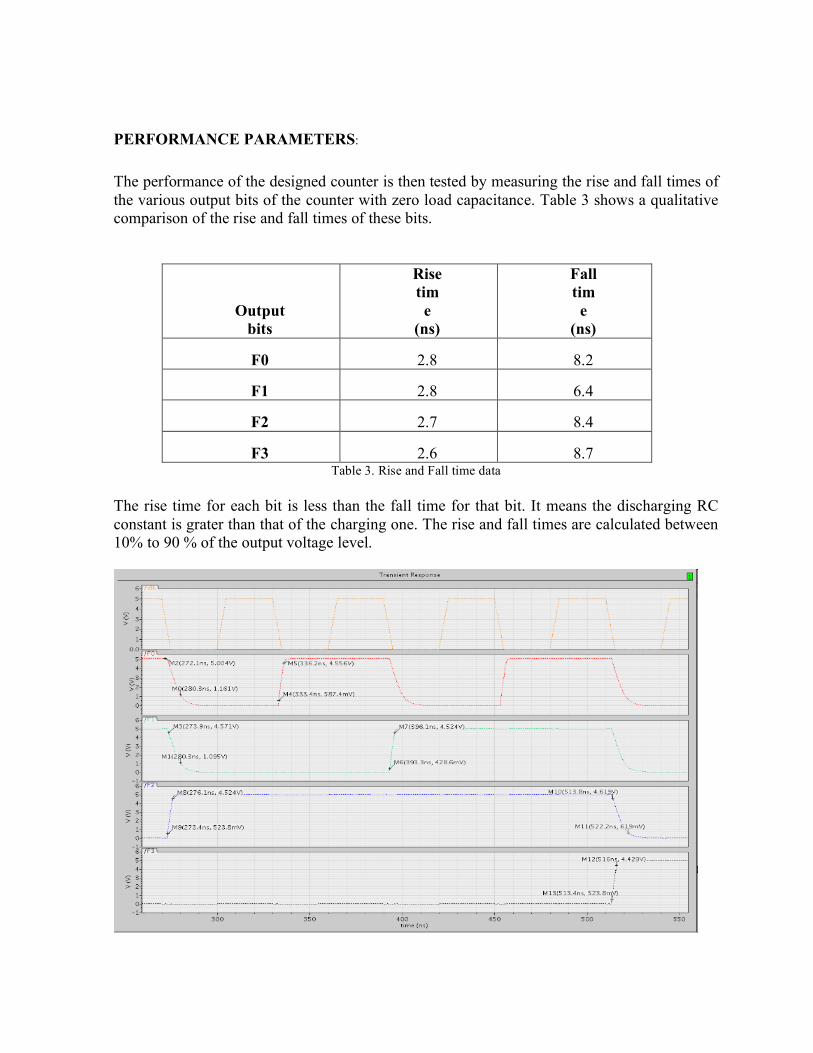
The performance of the designed counter is then tested by measuring the rise and fall times of the various output bits of the counter with zero load capacitance. Table 3 shows a qualitative comparison of the rise and fall times of these bits.
Output bits
Rise time
(ns)
Fall time
(ns)
F0 2.8 8.2
F1 2.8 6.4
F2 2.7 8.4
F3 2.6 8.7 Table 3. Rise and Fall time data
The rise time for each bit is less than the fall time for that bit. It means the discharging RC constant is grater than that of the charging one. The rise and fall times are calculated between 10% to 90 % of the output voltage level.
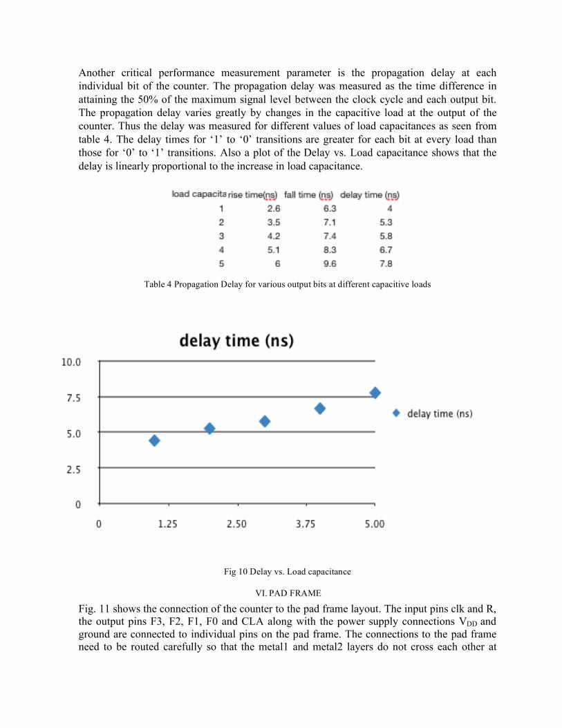
Another critical performance measurement parameter is the propagation delay at each individual bit of the counter. The propagation delay was measured as the time difference in attaining the 50% of the maximum signal level between the clock cycle and each output bit. The propagation delay varies greatly by changes in the capacitive load at the output of the counter. Thus the delay was measured for different values of load capacitances as seen from table 4. The delay times for ‘1’ to ‘0’ transitions are greater for each bit at every load than those for ‘0’ to ‘1’ transitions. Also a plot of the Delay vs. Load capacitance shows that the delay is linearly proportional to the increase in load capacitance.
Table 4 Propagation Delay for various output bits at different capacitive loads
Fig 10 Delay vs. Load capacitance
VI. PAD FRAME
Fig. 11 shows the connection of the counter to the pad frame layout. The input pins clk and R, the output pins F3, F2, F1, F0 and CLA along with the power supply connections VDD and ground are connected to individual pins on the pad frame. The connections to the pad frame need to be routed carefully so that the metal1 and metal2 layers do not cross each other at
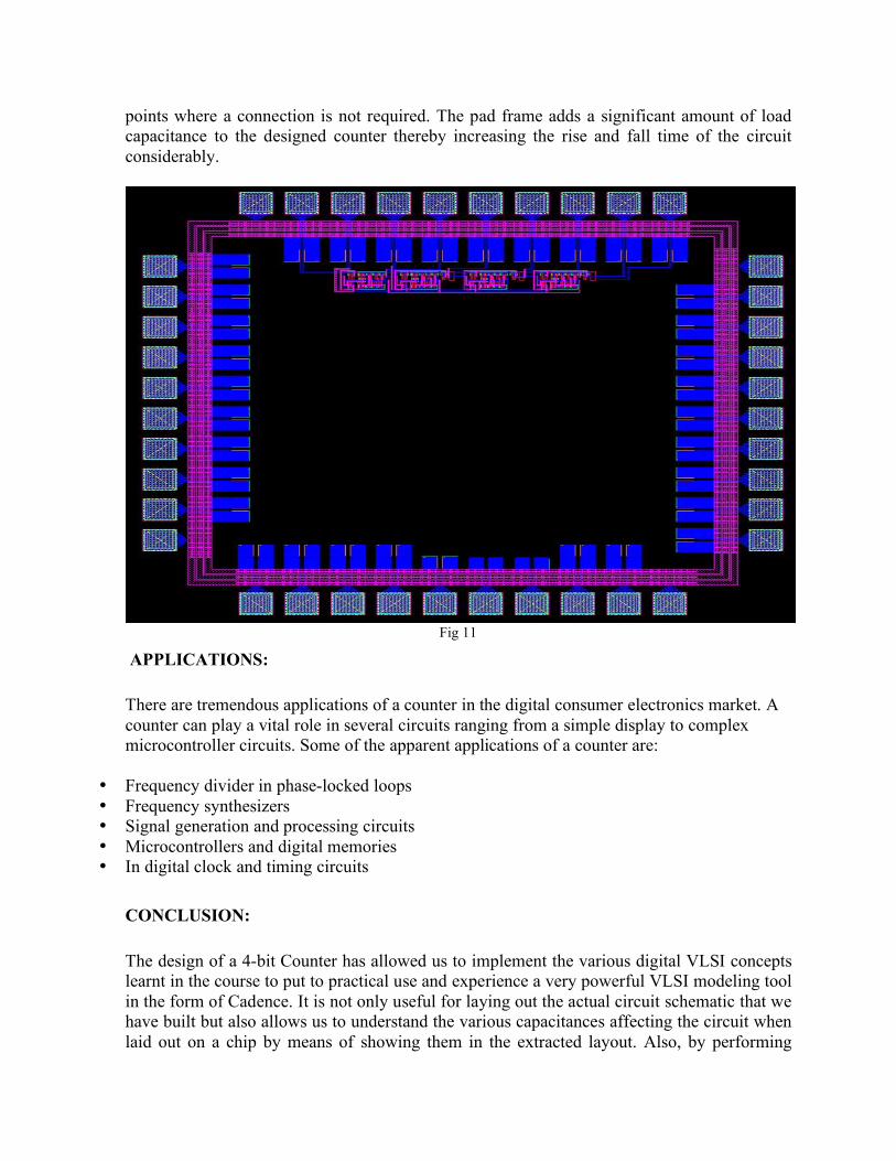
points where a connection is not required. The pad frame adds a significant amount of load capacitance to the designed counter thereby increasing the rise and fall time of the circuit considerably.
Fig 11
APPLICATIONS: There are tremendous applications of a counter in the digital consumer electronics market. A counter can play a vital role in several circuits ranging from a simple display to complex microcontroller circuits. Some of the apparent applications of a counter are:
• Frequency divider in phase-locked loops • Frequency synthesizers • Signal generation and processing circuits • Microcontrollers and digital memories • In digital clock and timing circuits
CONCLUSION: The design of a 4-bit Counter has allowed us to implement the various digital VLSI concepts learnt in the course to put to practical use and experience a very powerful VLSI modeling tool in the form of Cadence. It is not only useful for laying out the actual circuit schematic that we have built but also allows us to understand the various capacitances affecting the circuit when laid out on a chip by means of showing them in the extracted layout. Also, by performing

simulations in Cadence, it is possible to understand the effect of the varying the transistor sizes to obtain the desired output parameters. It is also useful to get know-how of the various design rules learnt and how they should be avoided to ensure a good working design with minimum capacitances and occupying the minimum chip area.