Embed Size (px)
Citation preview
General DescriptionThe MAX2880 is a high-performance phase-locked loop (PLL) capable of operating in both integer-N and fractional-N modes. Combined with an external reference oscillator, loop filter, and VCO, the device forms an ultra-low noise and low-spur frequency synthesizer capable of accepting RF input frequencies of up to 12.4GHz.The MAX2880 consists of a high-frequency and low-noise-phase frequency detector (PFD), precision charge pump, 10-bit programmable reference counter, 16-bit integer N counter, and 12-bit variable modulus fractional modulator.The MAX2880 is controlled by a 3-wire serial interface and is compatible with 1.8V control logic. The device is available in a lead-free, RoHS-compliant, 20-pin TQFN and 16-pin TSSOP packages, and operates over an extended -40°C to +85°C temperature range.
Applications Microwave Point-to-Point Systems Wireless Infrastructure Satellite Communications Test and Measurement RF DAC and ADC Clocks
Benefits and Features Integer and Fractional-N Modes 250MHz to 12.4GHz Broadband RF Input Normalized In-Band Noise Floor
• -229dBc/Hz in Integer Mode • -227dBc/Hz in Fractional Mode
-10dBm to +5dBm Wide Input Sensitivity Low-Noise Phase Frequency Detector
• 125MHz in Fractional Mode • 140MHz in Integer Mode
Reference Frequency Up to 210MHz Operates from +2.8V to +3.6V Supply Cycle Slip Reduction and Fast Lock Software and Hardware Shutdown Software Lock Detect On-Chip Temperature Sensor Compatible with +1.8V Control Logic Phase Adjustment
Ordering Information appears at end of data sheet.
19-6871; Rev 1; 11/15
MUX
x2
MUX
÷ 2 PFD CP
LD
DATLE
CLK
12-BITFRAC
12-BITMOD
NCOUNTER
SPI AND REGISTERS
REF
PROGRAMMABLE MAINMODULATOR
+
16-BITINT
MUX I/O
MUX
CE
RFINNRFINP
CP
VCP
MAX2880
MUX
÷ 2
REFDIV
MAX2880 250MHz to 12.4GHz, High-Performance, Fractional/Integer-N PLL
Functional Diagram
EVALUATION KIT AVAILABLE
VCC_ to GND_ ......................................................-0.3V to +3.9VVCP to GND_........................................................-0.3V to +5.8VCP to GND_ ............................................. -0.3V to (VCP + 0.3V)All Other Pins to GND_ .......................... -0.3V to (VCC_ + 0.3V)RFINP, RFINN ................................................................+10dBmContinuous Power Dissipation (TA = +70°C)
TQFN (derate 25.6mW/°C above +70°C)...............2051.3mW
Junction Temperature ......................................................+150°COperating Temperature Range ........................... -40°C to +85°CStorage Temperature Range ............................ -65°C to +150°CLead Temperature (soldering, 10s) ................................ +300°CSoldering Temperature (reflow) .......................................+260°C
TQFN Junction-to-Ambient Thermal Resistance (θJA) ..........39°C/W
Junction-to-Case Thermal Resistance (θJC) .................6°C/W
TSSOP Junction-to-Ambient Thermal Resistance (θJA) ..........90°C/W Junction-to-Case Thermal Resistance (θJC) ...............27°C/W
(Note 1)
(Measured using the MAX2880 Evaluation Kit. VCC_ = 3V to 3.6V, VCP = VCC_ to 5.5V, VGND_ = 0V, fREF = 50MHz, fPFD = 50MHz, TA = -40°C to +85°C. Typical values measured at VCC_ = 3.3V, VCP = 5V, TA = +25°C, no RF applied, Registers 0 through 4 settings: 303C0000, 00000009, 00008052, 00000BC3, 00000084, unless otherwise noted.) (Note 2)
(Measured using the MAX2880 Evaluation Kit. VCC_ = 3V to 3.6V, VCP = VCC_ to 5.5V, VGND_ = 0V, fREF = 50MHz, fPFD = 50MHz, fRFINN = 6000MHz, TA = -40°C to +85°C. Typical values measured at VCC_ = 3.3V, VCP = 5V, TA = +25°C, PRFINN = 2dBm, Registers 0 through 4 settings: 303C0000, 00000009, 00008052, 00000BC3, 00000084, unless otherwise noted.) (Note 2)
PARAMETER CONDITIONS MIN TYP MAX UNITS
Supply Voltage (VCC_) 2.8 3.3 3.6 V
Charge-Pump Supply (VCP) VCC_ 5.5 V
VCC_ Supply Current
PRE = 0, RFINN = 6GHz 39 50
mAPRE = 1, RFINN = 12GHz 49 59
Shutdown Mode 1
VCP Supply Current 0.65 2.0 mA
PARAMETER CONDITIONS MIN TYP MAX UNITS
Input Frequency 250 12,400 MHz
Input Power -10 +5 dBm
REF Input Frequency Range 10 210 MHz
REF Input Sensitivity 0.7 VCC_ VP-P
REF Input Capacitance 2 pF
REF Input Current -60 +60 µA
Phase Detector FrequencyFractional mode 125
MHzInteger mode 140
Sink/Source CurrentCP[3:0] = 1111, RRSET = 5.1kΩ 5.12
mACP[3:0] = 0000, RRSET = 5.1kΩ 0.32
MAX2880 250MHz to 12.4GHz, High-Performance, Fractional/Integer-N PLL
www.maximintegrated.com Maxim Integrated 2
Note 1: Package thermal resistances were obtained using the method described in JEDEC specification JESD51-7, using a four-layer board. For detailed information on package thermal considerations, refer to www.maximintegrated.com/thermal-tutorial.
Absolute Maximum Ratings
Package Thermal Characteristics
DC Electrical Characteristics
AC Electrical Characteristics
(VCC_ = 3V to 3.6V, VGND_ = 0V, TA = -40°C to +85°C. Typical values at VCC_ = 3.3V, TA = +25°C.) (Note 2)
(Measured using the MAX2880 Evaluation Kit. VCC_ = 3V to 3.6V, VCP = VCC_ to 5.5V, VGND_ = 0V, fREF = 50MHz, fPFD = 50MHz, fRFINN = 6000MHz, TA = -40°C to +85°C. Typical values measured at VCC_ = 3.3V, VCP = 5V, TA = +25°C, PRFINN = 2dBm, Registers 0 through 4 settings: 303C0000, 00000009, 00008052, 00000BC3, 00000084, unless otherwise noted.) (Note 2)
PARAMETER CONDITIONS MIN TYP MAX UNITS
RSET Range 2.7 10 kΩ
Charge-Pump Output Voltage 0.5 VCP - 0.5 V
In-Band Noise Floor Normalized (Note 3) -229 dBc/Hz
1/f Noise Normalized (Note 4) -122 dBc/Hz
In-Band Phase Noise (Note 5) -101 dBc/Hz
Integrated RMS Jitter (Note 6) 0.14 ps
Spurious Signals Due to PFD -84 dBc
ADC Resolution 7 Bits
Temperature Sensor Accuracy TA = -40°C to +85°C ±2.0 °C
PARAMETER SYMBOL CONDITIONS MIN TYP MAX UNITS
Input Logic-Level Low VIL 0.4 V
Input Logic-Level High VIH 1.5 V
Input Current IIH/IIL -1 +1 µA
Input Capacitance 1 pF
Output Logic-Level Low VOL 0.3mA sink current 0.4 V
Output Logic-Level High VOH 0.3mA source current VCC_ - 0.4 V
Output Current Level High IOH 0.5 mA
MAX2880 250MHz to 12.4GHz, High-Performance, Fractional/Integer-N PLL
www.maximintegrated.com Maxim Integrated 3
Digital I/O Characteristics
AC Electrical Characteristics (continued)
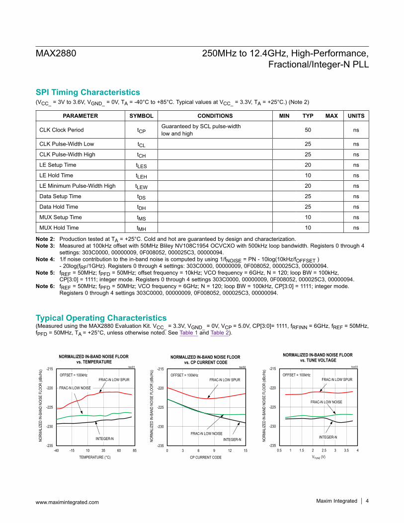
Note 2: Production tested at TA = +25°C. Cold and hot are guaranteed by design and characterization.Note 3: Measured at 100kHz offset with 50MHz Bliley NV108C1954 OCVCXO with 500kHz loop bandwidth. Registers 0 through 4
settings: 303C0000, 00000009, 0F008052, 000025C3, 00000094.Note 4: 1/f noise contribution to the in-band noise is computed by using 1/fNOISE = PN - 10log(10kHz/fOFFSET )
- 20log(fRF/1GHz). Registers 0 through 4 settings: 303C0000, 00000009, 0F008052, 000025C3, 00000094.Note 5: fREF = 50MHz; fPFD = 50MHz; offset frequency = 10kHz; VCO frequency = 6GHz, N = 120; loop BW = 100kHz,
CP[3:0] = 1111; integer mode. Registers 0 through 4 settings 303C0000, 00000009, 0F008052, 000025C3, 00000094.Note 6: fREF = 50MHz; fPFD = 50MHz; VCO frequency = 6GHz; N = 120; loop BW = 100kHz, CP[3:0] = 1111; integer mode.
Registers 0 through 4 settings 303C0000, 00000009, 0F008052, 000025C3, 00000094.
(VCC_ = 3V to 3.6V, VGND_ = 0V, TA = -40°C to +85°C. Typical values at VCC_ = 3.3V, TA = +25°C.) (Note 2)
(Measured using the MAX2880 Evaluation Kit. VCC_ = 3.3V, VGND_ = 0V, VCP = 5.0V, CP[3:0]= 1111, fRFINN = 6GHz, fREF = 50MHz, fPFD = 50MHz, TA = +25°C, unless otherwise noted. See Table 1 and Table 2).
PARAMETER SYMBOL CONDITIONS MIN TYP MAX UNITS
CLK Clock Period tCPGuaranteed by SCL pulse-width low and high 50 ns
CLK Pulse-Width Low tCL 25 ns
CLK Pulse-Width High tCH 25 ns
LE Setup Time tLES 20 ns
LE Hold Time tLEH 10 ns
LE Minimum Pulse-Width High tLEW 20 ns
Data Setup Time tDS 25 ns
Data Hold Time tDH 25 ns
MUX Setup Time tMS 10 ns
MUX Hold Time tMH 10 ns
-235
-230
-225
-220
-215
0 3 6 9 12 15
NORM
ALIZ
ED IN
-BAN
D NO
ISE
FLOO
R (d
Bc/H
z)
CP CURRENT CODE
NORMALIZED IN-BAND NOISE FLOOR vs. CP CURRENT CODE
toc02
INTEGER-NFRAC-N LOW NOISE
OFFSET = 100kHzFRAC-N LOW SPUR
-235
-230
-225
-220
-215
0.5 1 1.5 2 2.5 3 3.5 4
NORM
ALIZ
ED IN
-BAN
D NO
ISE
FLOO
R (d
Bc/H
z)
VTUNE (V)
NORMALIZED IN-BAND NOISE FLOOR vs. TUNE VOLTAGE
toc03
INTEGER-N
FRAC-N LOW NOISE
OFFSET = 100kHzFRAC-N LOW SPUR
-235
-230
-225
-220
-215
-40 -15 10 35 60 85
NORM
ALIZ
ED IN
-BAN
D NO
ISE
FLOO
R (d
Bc/H
z)
TEMPERATURE (°C)
NORMALIZED IN-BAND NOISE FLOOR vs. TEMPERATURE
toc01
INTEGER-N
FRAC-N LOW NOISE
OFFSET = 100kHzFRAC-N LOW SPUR
MAX2880 250MHz to 12.4GHz, High-Performance, Fractional/Integer-N PLL
www.maximintegrated.com Maxim Integrated 4
SPI Timing Characteristics
Typical Operating Characteristics
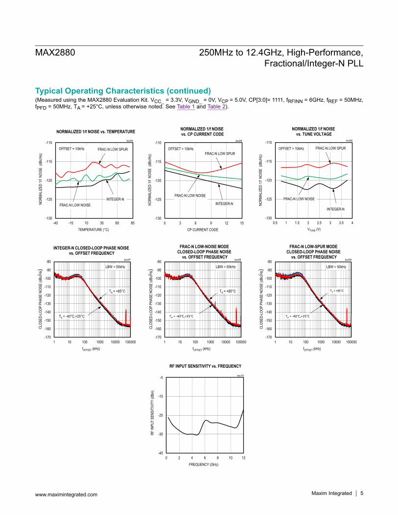
(Measured using the MAX2880 Evaluation Kit. VCC_ = 3.3V, VGND_ = 0V, VCP = 5.0V, CP[3:0]= 1111, fRFINN = 6GHz, fREF = 50MHz, fPFD = 50MHz, TA = +25°C, unless otherwise noted. See Table 1 and Table 2).
-130
-125
-120
-115
-110
0 3 6 9 12 15
NORM
ALIZ
ED 1/
f NOI
SE (
dBc/H
z)
CP CURRENT CODE
NORMALIZED 1/f NOISE vs. CP CURRENT CODE
toc05
INTEGER-N
FRAC-N LOW NOISE
OFFSET = 10kHzFRAC-N LOW SPUR
-130
-125
-120
-115
-110
0.5 1 1.5 2 2.5 3 3.5 4
NORM
ALIZ
ED 1/
f NOI
SE (
dBc/H
z)
VTUNE (V)
NORMALIZED 1/f NOISE vs. TUNE VOLTAGE
toc06
INTEGER-N
FRAC-N LOW NOISE
OFFSET = 10kHz FRAC-N LOW SPUR
-170
-160
-150
-140
-130
-120
-110
-100
-90
-80
1 10 100 1000 10000 100000
CLOS
ED-L
OOP
PHAS
E NO
ISE
(dBc
/Hz)
fOFFSET (kHz)
INTEGER-N CLOSED-LOOP PHASE NOISE vs. OFFSET FREQUENCY
toc07
LBW = 50kHz
TA = -40°C,+25°C
TA = +85°C
-170
-160
-150
-140
-130
-120
-110
-100
-90
-80
1 10 100 1000 10000 100000
CLOS
ED-L
OOP
PHAS
E NO
ISE
(dBc
/Hz)
fOFFSET (kHz)
FRAC-N LOW-NOISE MODE CLOSED-LOOP PHASE NOISE
vs. OFFSET FREQUENCYtoc08
LBW = 50kHz
TA = -40°C,+25°C
TA = +85°C
-170
-160
-150
-140
-130
-120
-110
-100
-90
-80
1 10 100 1000 10000 100000
CLOS
ED-L
OOP
PHAS
E NO
ISE
(dBc
/Hz)
fOFFSET (kHz)
FRAC-N LOW-SPUR MODE CLOSED-LOOP PHASE NOISE
vs. OFFSET FREQUENCYtoc09
LBW = 50kHz
TA = -40°C,+25°C
TA = +85°C
-45
-35
-25
-15
-5
0 2 4 6 8 10 12
RF IN
PUT
SENS
ITIV
ITY
(dBm
)
FREQUENCY (GHz)
RF INPUT SENSITIVITY vs. FREQUENCY
toc10
-130
-125
-120
-115
-110
-40 -15 10 35 60 85
NORM
ALIZ
ED 1/
f NOI
SE (
dBc/H
z)
TEMPERATURE (°C)
NORMALIZED 1/f NOISE vs. TEMPERATURE
toc04
INTEGER-NFRAC-N LOW NOISE
OFFSET = 10kHz FRAC-N LOW SPUR
MAX2880 250MHz to 12.4GHz, High-Performance, Fractional/Integer-N PLL
Maxim Integrated 5www.maximintegrated.com
Typical Operating Characteristics (continued)
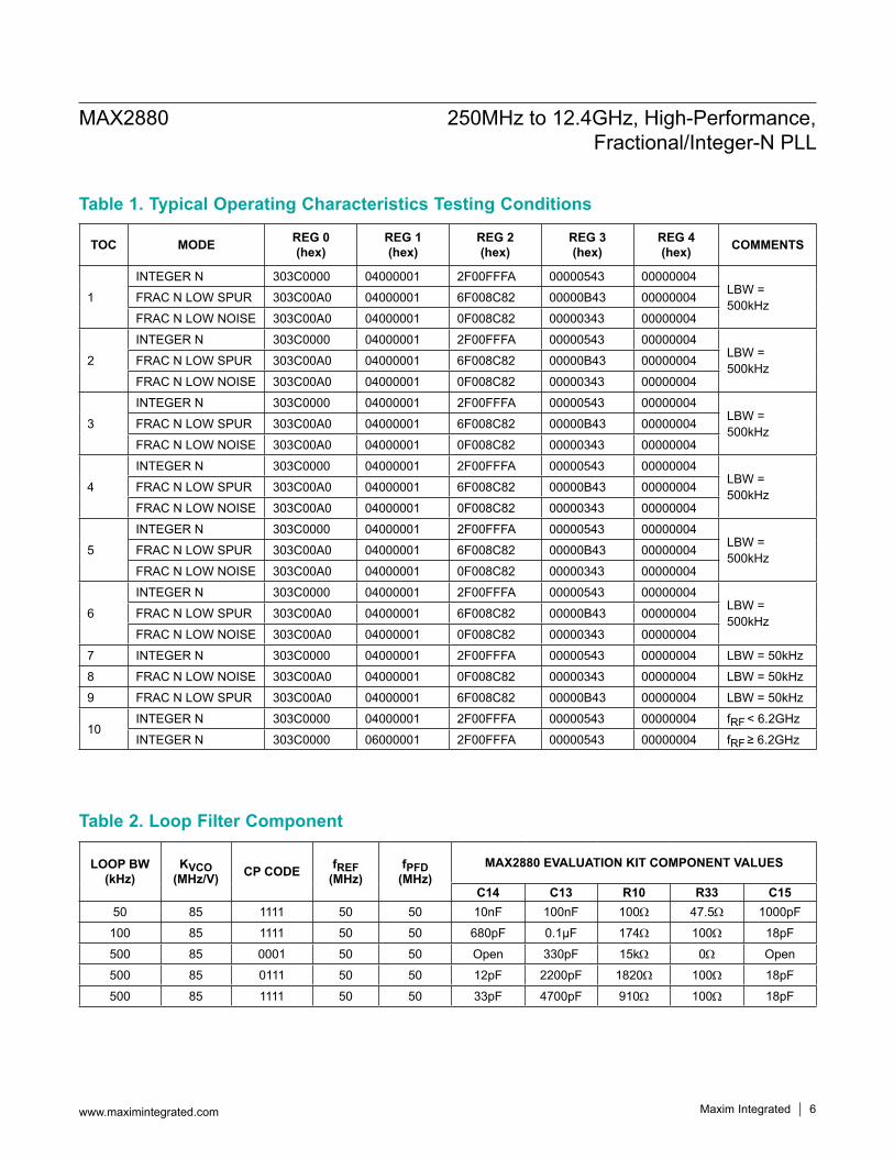
Table 1. Typical Operating Characteristics Testing Conditions
Table 2. Loop Filter Component
TOC MODE REG 0 (hex)
REG 1 (hex)
REG 2 (hex)
REG 3 (hex)
REG 4 (hex) COMMENTS
1
INTEGER N 303C0000 04000001 2F00FFFA 00000543 00000004LBW = 500kHzFRAC N LOW SPUR 303C00A0 04000001 6F008C82 00000B43 00000004
FRAC N LOW NOISE 303C00A0 04000001 0F008C82 00000343 00000004
2
INTEGER N 303C0000 04000001 2F00FFFA 00000543 00000004LBW = 500kHzFRAC N LOW SPUR 303C00A0 04000001 6F008C82 00000B43 00000004
FRAC N LOW NOISE 303C00A0 04000001 0F008C82 00000343 00000004
3
INTEGER N 303C0000 04000001 2F00FFFA 00000543 00000004LBW = 500kHzFRAC N LOW SPUR 303C00A0 04000001 6F008C82 00000B43 00000004
FRAC N LOW NOISE 303C00A0 04000001 0F008C82 00000343 00000004
4
INTEGER N 303C0000 04000001 2F00FFFA 00000543 00000004LBW = 500kHzFRAC N LOW SPUR 303C00A0 04000001 6F008C82 00000B43 00000004
FRAC N LOW NOISE 303C00A0 04000001 0F008C82 00000343 00000004
5
INTEGER N 303C0000 04000001 2F00FFFA 00000543 00000004LBW = 500kHzFRAC N LOW SPUR 303C00A0 04000001 6F008C82 00000B43 00000004
FRAC N LOW NOISE 303C00A0 04000001 0F008C82 00000343 00000004
6
INTEGER N 303C0000 04000001 2F00FFFA 00000543 00000004LBW = 500kHzFRAC N LOW SPUR 303C00A0 04000001 6F008C82 00000B43 00000004
FRAC N LOW NOISE 303C00A0 04000001 0F008C82 00000343 00000004
7 INTEGER N 303C0000 04000001 2F00FFFA 00000543 00000004 LBW = 50kHz
8 FRAC N LOW NOISE 303C00A0 04000001 0F008C82 00000343 00000004 LBW = 50kHz
9 FRAC N LOW SPUR 303C00A0 04000001 6F008C82 00000B43 00000004 LBW = 50kHz
10INTEGER N 303C0000 04000001 2F00FFFA 00000543 00000004 fRF < 6.2GHz
INTEGER N 303C0000 06000001 2F00FFFA 00000543 00000004 fRF ≥ 6.2GHz
LOOP BW (kHz)
KVCO(MHz/V) CP CODE fREF
(MHz)fPFD
(MHz)MAX2880 EVALUATION KIT COMPONENT VALUES
C14 C13 R10 R33 C1550 85 1111 50 50 10nF 100nF 100W 47.5W 1000pF
100 85 1111 50 50 680pF 0.1µF 174W 100W 18pF
500 85 0001 50 50 Open 330pF 15kW 0W Open
500 85 0111 50 50 12pF 2200pF 1820W 100W 18pF
500 85 1111 50 50 33pF 4700pF 910W 100W 18pF
MAX2880 250MHz to 12.4GHz, High-Performance, Fractional/Integer-N PLL
www.maximintegrated.com Maxim Integrated 6
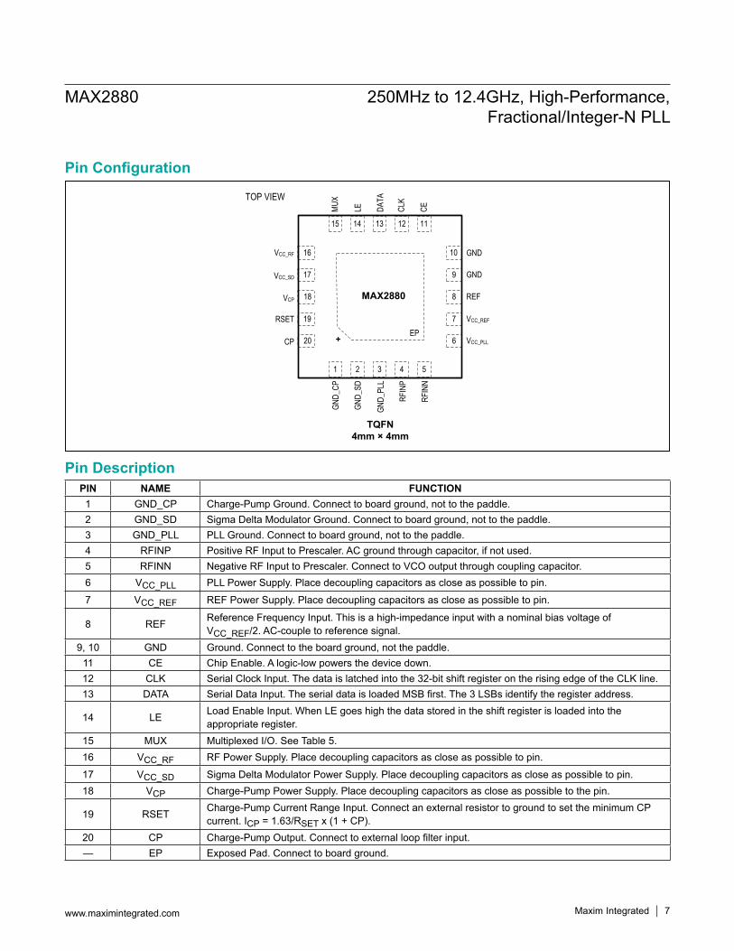
PIN NAME FUNCTION1 GND_CP Charge-Pump Ground. Connect to board ground, not to the paddle.2 GND_SD Sigma Delta Modulator Ground. Connect to board ground, not to the paddle.3 GND_PLL PLL Ground. Connect to board ground, not to the paddle.4 RFINP Positive RF Input to Prescaler. AC ground through capacitor, if not used.5 RFINN Negative RF Input to Prescaler. Connect to VCO output through coupling capacitor.6 VCC_PLL PLL Power Supply. Place decoupling capacitors as close as possible to pin.
7 VCC_REF REF Power Supply. Place decoupling capacitors as close as possible to pin.
8 REF Reference Frequency Input. This is a high-impedance input with a nominal bias voltage of VCC_REF/2. AC-couple to reference signal.
9, 10 GND Ground. Connect to the board ground, not the paddle.11 CE Chip Enable. A logic-low powers the device down. 12 CLK Serial Clock Input. The data is latched into the 32-bit shift register on the rising edge of the CLK line.13 DATA Serial Data Input. The serial data is loaded MSB first. The 3 LSBs identify the register address.
14 LE Load Enable Input. When LE goes high the data stored in the shift register is loaded into the appropriate register.
15 MUX Multiplexed I/O. See Table 5.16 VCC_RF RF Power Supply. Place decoupling capacitors as close as possible to pin.
17 VCC_SD Sigma Delta Modulator Power Supply. Place decoupling capacitors as close as possible to pin.18 VCP Charge-Pump Power Supply. Place decoupling capacitors as close as possible to the pin.
19 RSET Charge-Pump Current Range Input. Connect an external resistor to ground to set the minimum CP current. ICP = 1.63/RSET x (1 + CP).
20 CP Charge-Pump Output. Connect to external loop filter input.— EP Exposed Pad. Connect to board ground.
GND_
SD
RFIN
N
GND_
CP
LE CLK
CEMUX
VCP
RSET
CP
GND
REF
VCC_REF
VCC_PLL+
GND_
PLL
DATA
VCC_SD
GNDVCC_RF
TQFN4mm × 4mm
MAX2880
TOP VIEW
RFIN
P
10
9
8
7
6
1112131415
54321
16
17
18
19
20EP
MAX2880 250MHz to 12.4GHz, High-Performance, Fractional/Integer-N PLL
www.maximintegrated.com Maxim Integrated 7
Pin Description
Pin Configuration
MAX2880 250MHz to 12.4GHz, High-Performance, Fractional/Integer-N PLL
www.maximintegrated.com Maxim Integrated 8
16
15
14
13
12
11
10
1
2
3
4
5
6
7
VCP
VCC
MUX
LEGND
GND_CP
CP
RSET
TOP VIEW
MAX2880
DATA
CLK
CEVCC
INN
98 GNDREF
INP
16 TSSOP
+
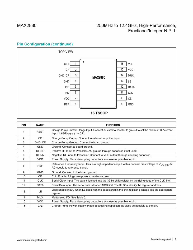
Pin Configuration (continued)
PIN NAME FUNCTION
1 RSET Charge-Pump Current Range Input. Connect an external resistor to ground to set the minimum CP current. ICP = 1.63/RSET x (1 + CP).
2 CP Charge-Pump Output. Connect to external loop filter input.3 GND_CP Charge-Pump Ground. Connect to board ground.4 GND Ground. Connect to board ground.5 RFINP Positive RF Input to Prescaler. AC ground through capacitor, if not used.6 RFINN Negative RF Input to Prescaler. Connect to VCO output through coupling capacitor.7 VCC Power Supply. Place decoupling capacitors as close as possible to pin.
8 REF Reference Frequency Input. This is a high-impedance input with a nominal bias voltage of VCC_REF/2. AC-couple to reference signal.
9 GND Ground. Connect to the board ground.10 CE Chip Enable. A logic-low powers the device down.11 CLK Serial Clock Input. The data is latched into the 32-bit shift register on the rising edge of the CLK line.
12 DATA Serial Data Input. The serial data is loaded MSB first. The 3 LSBs identify the register address.
13 LE Load Enable Input. When LE goes high the data stored in the shift register is loaded into the appropriate register.
14 MUX Multiplexed I/O. See Table 5.15 VCC Power Supply. Place decoupling capacitors as close as possible to pin.16 VCP Charge-Pump Power Supply. Place decoupling capacitors as close as possible to the pin.
Detailed Description4-Wire Serial InterfaceThe MAX2880 serial interface contains five read-write and one read-only 32-bit registers. The 29 most-significant bits (MSBs) are data, and the three least-significant bits (LSBs) are the register address. Register data is loaded MSB first through the 4-wire serial port interface (SPI). When latch enable (LE) is logic-low, the logic level at DATA is shifted at the rising edge of CLK. At the rising edge of LE, the 29 data bits are latched into the register selected by the address bits. Default values are not guar-anteed upon power-up. Program all register values after power-up.Register programming order should be address 0x04, 0x03, 0x02, 0x01, and 0x00. Several bits are dou ble buffered to update the settings at the same time. See the register descriptions for double buffered settings.
Any register can be read back through the MUX pin. The user must first set MUX bits = 0111. Next, write the regis-ter to be read, but with the READ bit of that register (the MSB) = 1. If the READ bit is set, the data of bits 30:3 do not matter because they are not latched into the register on a read operation. After the address bits are clocked and the LE pin is set, the MSB of that register appears on the MUX pin after the next rising edge on CLK pin. The MUX pin will continue to change after the rising edge of the next 28 clocks. After the LSB has been read, the user can reset the MUX bits to 0000.
Shutdown ModeThe MAX2880 can be put into shutdown mode by setting SHDN = 1 (register 3, bit 5) or by setting the CE pin to logic-low.
Figure 1. SPI Timing Diagram
Figure 2. Initiating Readback
LE
tDS tDH
tCL
tLEH
CLK
DATA BIT31 BIT30 BIT29 BIT1 BIT0
tLES
tCH
tCPtLEW
LE
CLK
32
DATA
3130291 33 34 35
tMS
tMH
36
DON’T CARE A2 A1 A0
MUX_OUT
MAX2880 250MHz to 12.4GHz, High-Performance, Fractional/Integer-N PLL
www.maximintegrated.com Maxim Integrated 9

Reference InputThe reference input stage is configured as a CMOS inverter with shunt resistance from input to output. In shut-down mode this input is set to high impedance to prevent loading of the reference source.The reference input signal path also includes optional x2 and ÷2 blocks. When the reference doubler is enabled (DBR = 1), the maximum reference input frequency is lim-ited to 100MHz. When the doubler is disabled, the refer-ence input frequency is limited to 205MHz. The minimum reference frequency is 10MHz. The minimum R counter divide ratio is 1, and the maximum divide ratio is 1023.
Int, Frac, Mod, and R Counter RelationshipThe phase-detector frequency is determined as follows:
fPFD = fREF x [(1 + DBR)/(R x (1 + RDIV2))]fREF represents the external reference input frequency. DBR (register 2, bit 20) sets the fREF input frequency doubler mode (0 or 1). RDIV2 (register 2, bit 21) sets the fREF divide-by-2 mode (0 or 1). R (register 2, bits 19:15) is the value of the 5-bit programmable reference counter (1 to 31). The maximum fPFD is 105MHz for Fractional-N and 140MHz for Integer-N. The R-divider can be held in reset when RST (register 3, bit 3) = 1.The VCO frequency is determined as follows:
fVCO = fPFD x (N + F/M) x (PRE + 1)N is the value of the 16-bit N counter (16 to 65535), pro-grammable through bits 30:27 (MSBs) of register 1 and bits 26:15 of register 0 (LSBs). M is the fractional modu-lus value (2 to 4095), programmable through bits 14:3 of register 2. F is the fractional division value (0 to MOD - 1), programmable through bits 14:3 of register 0. In fraction-al-N mode, the minimum N value is 19 and maximum N value is 4091. The N counter is held in reset when RST = 1 (register 3, bit 3). PRE is RF input prescaler control where 0 = divide-by-1, and 1 = divide-by-2 (register 1, bit 25). If the RF input frequency is above 6.2GHz, then set PRE = 1.
Integer-N/Fractional-N ModesInteger-N mode is selected by setting bit INT = 1 (reg-ister 3, bit 10). When operating in integer-N mode, it is also necessary to set bit Lock Detect Function, LDF = 1 (register 3, bit 9) to set the lock detect to integer-N mode.The device’s fractional-N mode is selected by setting bit INT = 0 (register 3, bit 10). Additionally, set bit LDF = 0 (register 3, bit 9) for fractional-N lock-detect mode.If the device is in fractional-N mode, it will remain in frac-tional-N mode when fractional division value F = 0, which can result in unwanted spurs. To avoid this condition, the device can automatically switch to integer-N mode when F = 0 if the bit F01 = 1 (register 4, bit 29).
Phase Detector and Charge PumpThe device’s charge-pump current is determined by the value of the resistor from pin RSET to ground and the value of bits CP (register 2, bits 27:24) as follows:
ICP = 1.63/RSET x (1 + CP)When operating in the fractional-N mode, the charge-pump linearity (CPL) bits can be adjusted by the user to optimize in-band noise and spur levels. In the integer-N mode, CPL must be set to 0. If lower noise operation in integer-N mode is desired, set the charge-pump output clamp bit CPOC = 1 (register 3, bit 13) to prevent leak-age current into the loop filter. In fractional-N mode, set CPOC = 0..The charge-pump output can be put into high-impedance mode when TRI = 1 (register 3, bit 4). The output is in normal mode when TRI = 0.The phase detector polarity can be changed if an active inverting loop filter topology is used. For noninverting loop filters, set PDP = 1 (register 3, bit 6). For inverting loop filters, set PDP = 0.
Figure 3. Reference Input
REF_INX2
DIVIDE-BY-2R COUNTER MUXMUX TO PFD
MAX2880 250MHz to 12.4GHz, High-Performance, Fractional/Integer-N PLL
www.maximintegrated.com Maxim Integrated 10
MUX and Lock DetectMUX is a multipurpose test output for observing various internal functions of the MAX2880. MUX can also be configured as serial data output. MUX bits (register 0, bit 30:27) are used to select the desired MUX signal (see Table 5).The digital lock detect is dependent on the mode of the synthesizer. In fractional-N mode set LDF = 0, and in integer-N mode set LDF = 1. To set the accuracy of the digital lock detect, see Table 3 and Table 4.
Cycle Slip ReductionCycle slip reduction is one of two available methods to improve lock time. It is enabled by setting CSR bit (regis-ter 2, bit 28) to 1. In this mode, the charge pump must be set for its minimum value.
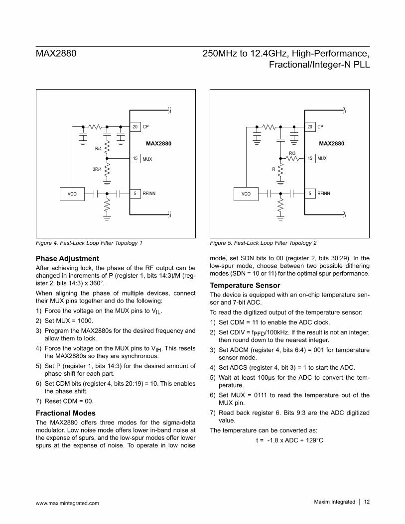
Fast-LockFast-lock is the other method available for improving lock time by temporarily increasing the loop bandwidth at the start of the locking cycle. It is enabled by setting the CDM bits to 01 (register 4, bits 20:19). In addition, the charge-pump current has to be set to CP = 0000 (register 2, bits 27:24), MUX bits configured to 1100 (register 0, bits 30:27), and the shunt resistive portion of the loop filter has to be segmented into two parts, where one resistor is 1/4 of the total resistance, and the other resistor is 3/4 of the total resistance. Figure 4 and Figure 5 illustrate the two
possible topologies. Once enabled, fast lock is activated after writing to register 0. During this process, the charge pump is automatically increased to its maximum (CP bits = 1111) and the shunt loop filter resistance is reduced to 1/4 of the total resistance when the internal switch shorts the MUX pin to ground. Bits CDIV (register 4, bits 18:7) control the time spent in the wide bandwidth mode. The time spent in the fast lock is:
t = CDIV/fPFDThe time should be set long enough to allow the loop to settle before switching back to the lower loop bandwidth.
RF InputsThe differential RF inputs are connected to a high-imped-ance input buffer which drives a demultiplexer for select-ing between two RF input frequency ranges: 250MHz to 6.2GHz and 6.2GHz to 12.4GHz. When the RF input fre-quency is 250MHz to 6.2GHz, the fixed divide-by-2 pres-caler is bypassed by setting bit PRE to 0. When the RF input frequency is 6.2GHz to 12.4GHz, the fixed divide-by-2 path is selected by setting PRE to 1. The supported input power range is -10dBm to +5dBm. For single-ended operation, terminate the unused RF input to GND through a 100pF capacitor.Since the RF input of the device is high impedance, a DC isolated external shunt resistor is used to provide the 50Ω input impedance for the system (see the Typical Application Circuit).
Table 3. Fractional-N Digital Lock-Detect Settings
Table 4. Integer-N Digital Lock-Detect Settings
PFD FREQUENCY (MHz) LDS LDP LOCKED UP/DOWN
TIME SKEW (ns)NUMBER OF LOCKED CYCLES TO SET LD
TIME SKEW TO UNSET LD (ns)
≤ 32 0 0 10 40 15
≤ 32 0 1 6 40 15
> 32 1 X 4 40 4
PFD FREQUENCY (MHz) LDS LDP LOCKED UP/DOWN
TIME SKEW (ns)NUMBER OF LOCKED CYCLES TO SET LD
TIME SKEW TO UNSET LD (ns)
≤ 32 0 0 10 5 15
≤ 32 0 1 6 5 15
> 32 1 X 4 5 4
MAX2880 250MHz to 12.4GHz, High-Performance, Fractional/Integer-N PLL
www.maximintegrated.com Maxim Integrated 11
Phase AdjustmentAfter achieving lock, the phase of the RF output can be changed in increments of P (register 1, bits 14:3)/M (reg-ister 2, bits 14:3) x 360°.When aligning the phase of multiple devices, connect their MUX pins together and do the following:1) Force the voltage on the MUX pins to VIL.2) Set MUX = 1000.3) Program the MAX2880s for the desired frequency and
allow them to lock.4) Force the voltage on the MUX pins to VIH. This resets
the MAX2880s so they are synchronous.5) Set P (register 1, bits 14:3) for the desired amount of
phase shift for each part.6) Set CDM bits (register 4, bits 20:19) = 10. This enables
the phase shift.7) Reset CDM = 00.
Fractional ModesThe MAX2880 offers three modes for the sigma-delta modulator. Low noise mode offers lower in-band noise at the expense of spurs, and the low-spur modes offer lower spurs at the expense of noise. To operate in low noise
mode, set SDN bits to 00 (register 2, bits 30:29). In the low-spur mode, choose between two possible dithering modes (SDN = 10 or 11) for the optimal spur performance.
Temperature SensorThe device is equipped with an on-chip temperature sen-sor and 7-bit ADC.To read the digitized output of the temperature sensor:1) Set CDM = 11 to enable the ADC clock.2) Set CDIV = fPFD/100kHz. If the result is not an integer,
then round down to the nearest integer.3) Set ADCM (register 4, bits 6:4) = 001 for temperature
sensor mode.4) Set ADCS (register 4, bit 3) = 1 to start the ADC.5) Wait at least 100µs for the ADC to convert the tem-
perature.6) Set MUX = 0111 to read the temperature out of the
MUX pin.7) Read back register 6. Bits 9:3 are the ADC digitized
value.The temperature can be converted as:
t = -1.8 x ADC + 129°C
Figure 4. Fast-Lock Loop Filter Topology 1 Figure 5. Fast-Lock Loop Filter Topology 2
VCO
20
15
5
CP
MAX2880
RFINN
R/4
3R/4
MUX
VCO
20
15
5
CP
MUX
RFINN
R
R/3
MAX2880
MAX2880 250MHz to 12.4GHz, High-Performance, Fractional/Integer-N PLL
www.maximintegrated.com Maxim Integrated 12
Register and Bit DescriptionsThe operating mode of the MAX2880 is controlled via 5 read/write on-chip registers and 1 read-only register.
Defaults are not guaranteed upon power-up and are pro-vided for reference only. All reserved bits should only be written with default values. In shutdown mode, the regis-ter values are retained.
Table 5. Register 0 (Address: 000, Default: 383C0000 Hex)BIT LOCATION BIT ID NAME DEFINITION
31 READ READ 0 = Write to register1 = Read from register
30:27 MUX[3:0] MUX Mode
Sets MUX Pin Configuration0000 = High-Impedance Output0001 = D_VDD0010 = D_GND0011 = R Divider Output0100 = N Divider Output0101 = Analog Lock Detect0110 = Digital Lock Detect0111 = SPI Output1000 = SYNC input1001 = Reserved1010 = Reserved1011 = Reserved1100 = Fast Lock1101 = R Divider/21110 = N Divider/21111 = Reserved
26:15 N[11:0] Integer Division Value
Sets integer part (N divider) of the feedback divider factor. MSBs are located in register 1. All integer values from 16 to 65,535 are allowed for integer mode. Integer values from 19 to 4091 are allowed for fractional mode.
14:3 F[11:0] Fractional Division Value
Sets Fractional Value. Allowed F values are 0 to M-1.000000000000 = 0 (see F01 bit description)000000000001 = 1----111111111110 = 4094111111111111 = 4095
2:0 ADDR[2:0] Address Bits Register address bits
MAX2880 250MHz to 12.4GHz, High-Performance, Fractional/Integer-N PLL
www.maximintegrated.com Maxim Integrated 13
Table 6. Register 1 (Address: 001, Default: 00000001 Hex)
Table 7. Register 2 (Address: 010, Default: 0000FFFA Hex)
*Bits double buffered by Register 0.
BIT LOCATION BIT ID NAME DEFINITION
31 READ Register Read 0 = Write to register1 = Read from register
30:27 N[15:12] Integer Division Value
Sets Integer part (N divider) of the feedback divider factor. LSBs are located in register 0. All integer values from 16 to 65,535 are allowed for integer mode. Integer values from 19 to 4091 are allowed for fractional mode.
26 Unused Unused Set to 0
25 PRE RF Input Prescaler
Sets RF Input prescaler to divide-by-1 or divide-by-20 = Divide-by-1 (250MHz to 6.2GHz)1 = Divide-by-2 (6.2GHz to 12.4GHz)
24:20 Unused Unused Set to all 0’s.
19:15* R[9:5] Reference Divider Mode
Sets Reference Divide Value (R). LSBs located in register 2.0000000000 = 0 (Unused)0000000001 = 1-----1111111111 = 1023
14:3 P[11:0] Phase Value
Sets Phase Value.See the Phase Adjustment section000000000000 = 0000000000001 = 1-----111111111111 = 4095
2:0 ADDR[2:0] Address Bits Register address bits
BIT LOCATION BIT ID NAME DEFINITION
31 READ Register Read 0 = Write to register1 = Read from register
30:29 SDN[1:0] Fractional-N Modes
Sets Noise Mode (see the Fractional Modes section under the Detailed Description):00 = Low-Noise Mode01 = Reserved10 = Low-Spur Mode 111 = Low-Spur Mode 2
28 CSR Cycle Slip Reduction
0 = Cycle Slip Reduction disabled1 = Cycle Slip Reduction enabled
MAX2880 250MHz to 12.4GHz, High-Performance, Fractional/Integer-N PLL
www.maximintegrated.com Maxim Integrated 14
Table 8. Register 3 (Address: 011, Default: 00000043 Hex)
Table 7. Register 2 (Address: 010, Default: 0000FFFA Hex) (continued)
*Bits double buffered by Register 0.
BIT LOCATION BIT ID NAME DEFINITION
27:24 CP[3:0] Charge-Pump Current
Sets Charge-Pump Current[ICP = 1.63/RSET x (1 + CP[3:0])]
23:22 Unused Unused Factory Use Only, set to 00.
21* RDIV2 Reference Div2 Mode
Sets Reference Divider Mode0 = Disable reference divide by 21 = Enable reference divide by 2
20* DBR Reference Doubler Mode
Sets Reference Doubler Mode0 = Disable reference doubler1 = Enable reference doubler
19:15* R[4:0] Reference Divider Mode
Sets Reference Divide Value (R). Double buffered by Register 0. MSBs located in register 1.0000000000 = 0 (Unused)0000000001 = 1-----1111111111 = 1023
14:3* M[11:0] Modulus Value
Fractional Modulus value used to program fVCO. See the Int, Frac, Mod, And R Counter Relationship section. Double buffered by register 0.000000000000 = Unused000000000001 = Unused000000000010 = 2-----111111111111 = 4095
2:0 ADDR Address Bits Register address
BIT LOCATION BIT ID NAME DEFINITION
31 READ Register Read 0 = Write to register1 = Read from register
30:18 Unused Unused Write to all 0’s
17 F01 F01Sets integer mode for F =0.0 = If F[11:0] = 0, then fractional-N mode is set1 = If F[11:0] = 0, then integer-N mode is auto set
16:15 CPT[1:0] Charge-Pump Test
Sets Charge-Pump Test Modes00 = Normal mode01 = Reserved10 = Force CP into source mode11 = Force CP into Sink mode
14 RSTSD Sigma Delta Reset
0 = Reset Sigma Delta Modulator to known value after each write to register 0 1 = Do not reset Sigma Delta Modulator to known value after each write to register 0
MAX2880 250MHz to 12.4GHz, High-Performance, Fractional/Integer-N PLL
www.maximintegrated.com Maxim Integrated 15
Table 8. Register 3 (Address: 011, Default: 00000043 Hex) (continued)BIT LOCATION BIT ID NAME DEFINITION
13 CPOC CP Output Clamp
Sets Charge-Pump Output Clamp Mode0 = Disables clamping of the CP output when the CP is off.1 = Enables the clamping of the CP output when the CP is off (improved integer-N in-band phase noise).
12:11 CPL[1:0] CP Linearity
Sets CP Linearity Mode00 = Disables the CP linearity mode (integer-N mode).01 = Enables the CP linearity mode (Fractional-N mode)10 = Enables the CP linearity mode (Fractional-N mode)11 = Enables the CP linearity mode (Fractional-N mode)
10 INT Integer ModeControls Synthesizer Integer or Fractional-N Mode0 = Fractional-N mode1 = Integer mode
9 LDF Lock Detect Function
Sets Lock Detect Function0 = Fractional-N lock detect1 = Integer-N lock detect
8 LDS Lock Detect Speed
Lock Detect Speed Adjustment0 = fPFD ≤ 32MHz1 = fPFD > 32MHz
7 LDP Lock Detect Precision
Sets Lock Detect Precision0 = 10ns1 = 6ns
6 PDP Phase Detector Polarity
Sets Phase Detector Polarity0 = Negative (for use with inverting active loop filters) 1 = Positive (for use with passive loop filers and noninverting active loop filters)
5 SHDN Shutdown Mode
Sets Power-Down Mode0 = Normal mode1 = Device shutdown
4 TRI
Charge-Pump High-Impedance
Mode
Sets Charge-Pump High-Impedance Mode0 = Disabled1 = Enabled
3 RST Counter ResetSets Counter Reset Mode0 = Normal operation1 = R and N counters reset
2:0 ADDR[2:0] Address Bits Register address
MAX2880 250MHz to 12.4GHz, High-Performance, Fractional/Integer-N PLL
www.maximintegrated.com Maxim Integrated 16
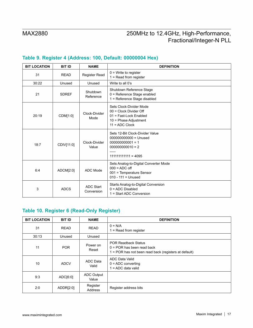
Table 10. Register 6 (Read-Only Register)
Table 9. Register 4 (Address: 100, Default: 00000004 Hex)BIT LOCATION BIT ID NAME DEFINITION
31 READ Register Read 0 = Write to register1 = Read from register
30:22 Unused Unused Write to all 0’s
21 SDREF Shutdown Reference
Shutdown Reference Stage0 = Reference Stage enabled1 = Reference Stage disabled
20:19 CDM[1:0] Clock-Divider Mode
Sets Clock-Divider Mode00 = Clock Divider Off01 = Fast-Lock Enabled10 = Phase Adjustment11 = ADC Clock
18:7 CDIV[11:0] Clock-Divider Value
Sets 12-Bit Clock-Divider Value000000000000 = Unused000000000001 = 1000000000010 = 2-----111111111111 = 4095
6:4 ADCM[2:0] ADC Mode
Sets Analog-to-Digital Converter Mode000 = ADC off001 = Temperature Sensor010 - 111 = Unused
3 ADCS ADC Start Conversion
Starts Analog-to-Digital Conversion0 = ADC Disabled1 = Start ADC Conversion
BIT LOCATION BIT ID NAME DEFINITION
31 READ READ 0 = N/A1 = Read from register
30:13 Unused Unused
11 POR Power on Reset
POR Readback Status0 = POR has been read back1 = POR has not been read back (registers at default)
10 ADCV ADC Data Valid
ADC Data Valid0 = ADC converting1 = ADC data valid
9:3 ADC[6:0] ADC Output Value
2:0 ADDR[2:0] Register Address Register address bits
MAX2880 250MHz to 12.4GHz, High-Performance, Fractional/Integer-N PLL
www.maximintegrated.com Maxim Integrated 17
GND_
SD
RFIN
N
GND_
CP
LE CLK
CEMUX
VCP
RSET
CP
GND
REF
VCC_REF
VCC_PLL+
GND_
PLL
DATA
VCC_SD
GNDVCC_RF
MAX2880
RFIN
P
10
9
8
7
6
1112131415
54321
16
17
18
19
20
EP
VCO
VCC
VCC
VCC
VCC
SPI INTERFACE
RFOUT
VCP
5.1kΩR1
C14
C15
R33C13
R10
51Ω
100pF100pF
VCO
2
4
5
6
7
8
16
15
14
13
12
11
10
9
1
3
50W
RFOUT
SPI INTERFACE
VCP
VCCRSET
CP
GND_CP
GND
RFINP
RFINN
VCC
5.1kW
REF
VCP
VCC
MUX
LE
DATA
CLK
CE
GND
VCC
MAX2880
MAX2880 250MHz to 12.4GHz, High-Performance, Fractional/Integer-N PLL
www.maximintegrated.com Maxim Integrated 18
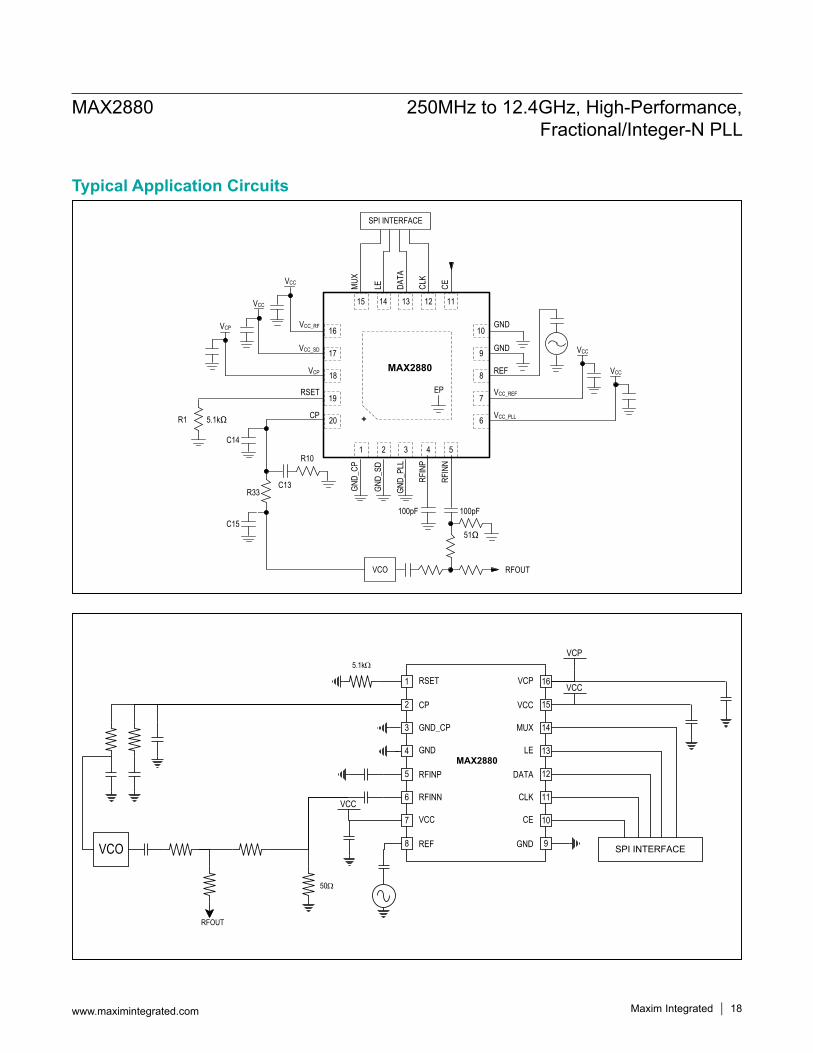
Typical Application Circuits
+Denotes lead(Pb)-free/RoHS-compliant package.*EP = Exposed pad.
PART TEMP RANGE PIN-PACKAGEMAX2880ETP+ -40°C to +85°C 20 TQFN-EP*
MAX2880EUE+ -40°C to +85°C 16 TSSOP
PACKAGE TYPE
PACKAGE CODE
OUTLINE NO.
LAND PATTERN NO.
20 TQFN-EP T2044+2 21-0139 90-003616 TSSOP T16+1 21-0066 90-0117
MAX2880 250MHz to 12.4GHz, High-Performance, Fractional/Integer-N PLL
www.maximintegrated.com Maxim Integrated 19
Package InformationFor the latest package outline information and land patterns (footprints), go to www.maximintegrated.com/packages. Note that a “+”, “#”, or “-” in the package code indicates RoHS status only. Package drawings may show a different suffix character, but the drawing pertains to the package regardless of RoHS status.
Ordering Information
REVISIONNUMBER
REVISIONDATE DESCRIPTION PAGES
CHANGED
0 12/13 Initial release —
1 11/15 Added TSSOP package information and updated Table 9 1, 4, 10, 18–20
Maxim Integrated cannot assume responsibility for use of any circuitry other than circuitry entirely embodied in a Maxim Integrated product. No circuit patent licenses are implied. Maxim Integrated reserves the right to change the circuitry and specifications without notice at any time. The parametric values (min and max limits) shown in the Electrical Characteristics table are guaranteed. Other parametric values quoted in this data sheet are provided for guidance.
Maxim Integrated and the Maxim Integrated logo are trademarks of Maxim Integrated Products, Inc.
MAX2880 250MHz to 12.4GHz, High-Performance, Fractional/Integer-N PLL
© 2015 Maxim Integrated Products, Inc. 20
Revision History
For pricing, delivery, and ordering information, please contact Maxim Direct at 1-888-629-4642, or visit Maxim Integrated’s website at www.maximintegrated.com.