Embed Size (px)
Citation preview
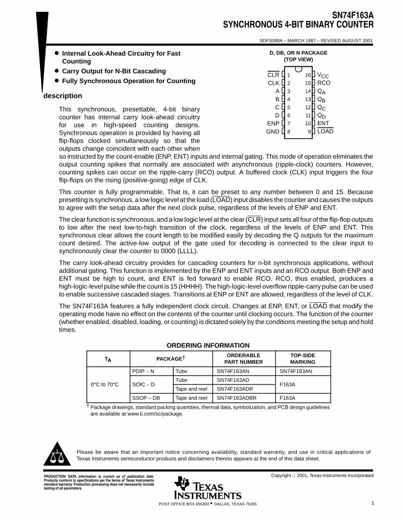
SN74F163ASYNCHRONOUS 4-BIT BINARY COUNTER
SDFS088A – MARCH 1987 – REVISED AUGUST 2001
1POST OFFICE BOX 655303 • DALLAS, TEXAS 75265
Internal Look-Ahead Circuitry for FastCounting
Carry Output for N-Bit Cascading
Fully Synchronous Operation for Counting
description
This synchronous, presettable, 4-bit binarycounter has internal carry look-ahead circuitryfor use in high-speed counting designs.Synchronous operation is provided by having allflip-flops clocked simultaneously so that theoutputs change coincident with each other whenso instructed by the count-enable (ENP, ENT) inputs and internal gating. This mode of operation eliminates theoutput counting spikes that normally are associated with asynchronous (ripple-clock) counters. However,counting spikes can occur on the ripple-carry (RCO) output. A buffered clock (CLK) input triggers the fourflip-flops on the rising (positive-going) edge of CLK.
This counter is fully programmable. That is, it can be preset to any number between 0 and 15. Becausepresetting is synchronous, a low logic level at the load (LOAD) input disables the counter and causes the outputsto agree with the setup data after the next clock pulse, regardless of the levels of ENP and ENT.
The clear function is synchronous, and a low logic level at the clear (CLR) input sets all four of the flip-flop outputsto low after the next low-to-high transition of the clock, regardless of the levels of ENP and ENT. Thissynchronous clear allows the count length to be modified easily by decoding the Q outputs for the maximumcount desired. The active-low output of the gate used for decoding is connected to the clear input tosynchronously clear the counter to 0000 (LLLL).
The carry look-ahead circuitry provides for cascading counters for n-bit synchronous applications, withoutadditional gating. This function is implemented by the ENP and ENT inputs and an RCO output. Both ENP andENT must be high to count, and ENT is fed forward to enable RCO. RCO, thus enabled, produces ahigh-logic-level pulse while the count is 15 (HHHH). The high-logic-level overflow ripple-carry pulse can be usedto enable successive cascaded stages. Transitions at ENP or ENT are allowed, regardless of the level of CLK.
The SN74F163A features a fully independent clock circuit. Changes at ENP, ENT, or LOAD that modify theoperating mode have no effect on the contents of the counter until clocking occurs. The function of the counter(whether enabled, disabled, loading, or counting) is dictated solely by the conditions meeting the setup and holdtimes.
ORDERING INFORMATION
TA PACKAGE† ORDERABLEPART NUMBER
TOP-SIDEMARKING
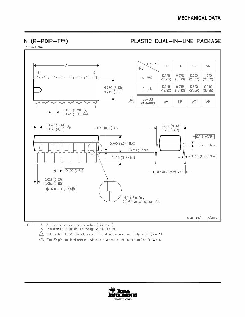
PDIP – N Tube SN74F163AN SN74F163AN
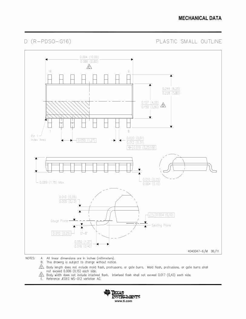
0°C to 70°C SOIC DTube SN74F163AD
F163A0°C to 70°C SOIC – DTape and reel SN74F163ADR
F163A
SSOP – DB Tape and reel SN74F163ADBR F163A
† Package drawings, standard packing quantities, thermal data, symbolization, and PCB design guidelinesare available at www.ti.com/sc/package.
Copyright 2001, Texas Instruments IncorporatedPRODUCTION DATA information is current as of publication date.Products conform to specifications per the terms of Texas Instrumentsstandard warranty. Production processing does not necessarily includetesting of all parameters.
Please be aware that an important notice concerning availability, standard warranty, and use in critical applications ofTexas Instruments semiconductor products and disclaimers thereto appears at the end of this data sheet.
D, DB, OR N PACKAGE(TOP VIEW)
1
2
3
4
5
6
7
8
16
15
14
13
12
11
10
9
CLRCLK
ABCD
ENPGND
VCCRCOQAQBQCQDENTLOAD
SN74F163ASYNCHRONOUS 4-BIT BINARY COUNTER
SDFS088A – MARCH 1987 – REVISED AUGUST 2001
2 POST OFFICE BOX 655303 • DALLAS, TEXAS 75265
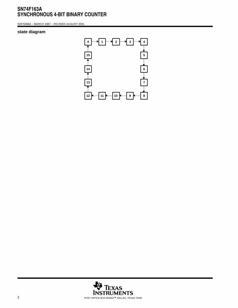
state diagram
0
15
14
13
12
1 2 3 4
5
6
7
891011
SN74F163ASYNCHRONOUS 4-BIT BINARY COUNTER
SDFS088A – MARCH 1987 – REVISED AUGUST 2001
3POST OFFICE BOX 655303 • DALLAS, TEXAS 75265
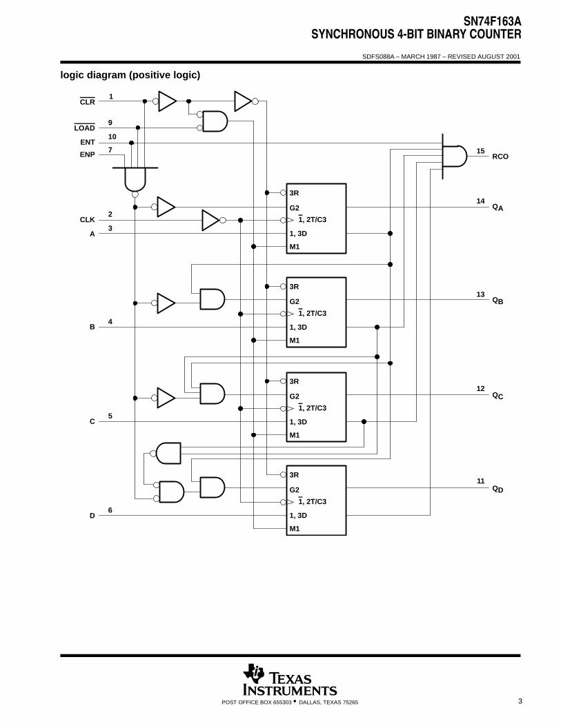
logic diagram (positive logic)
3R
G2
1, 3D
M1
1, 2T/C3
3R
G2
1, 3D
M1
1, 2T/C3
3R
G2
1, 3D
M1
1, 2T/C3
3R
G2
1, 3D
M1
1, 2T/C3
1
9
10
7
2
3
4
5
6
15
14
13
12
11
CLR
LOAD
ENT
ENP
CLK
A
B
C
D
RCO
QA
QB
QC
QD
SN74F163ASYNCHRONOUS 4-BIT BINARY COUNTER
SDFS088A – MARCH 1987 – REVISED AUGUST 2001
4 POST OFFICE BOX 655303 • DALLAS, TEXAS 75265
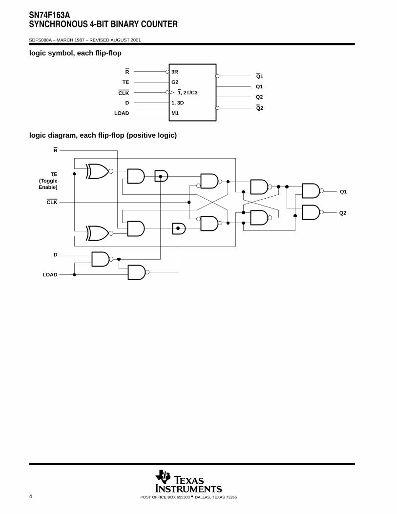
logic symbol, each flip-flop
3R
G2TEQ1
1, 3DD
M1LOAD
Q21, 2T/C3
R
CLK
Q1
Q2
logic diagram, each flip-flop (positive logic)
R
CLK
D
LOAD
TE(ToggleEnable)
Q1
Q2
SN74F163ASYNCHRONOUS 4-BIT BINARY COUNTER
SDFS088A – MARCH 1987 – REVISED AUGUST 2001
5POST OFFICE BOX 655303 • DALLAS, TEXAS 75265
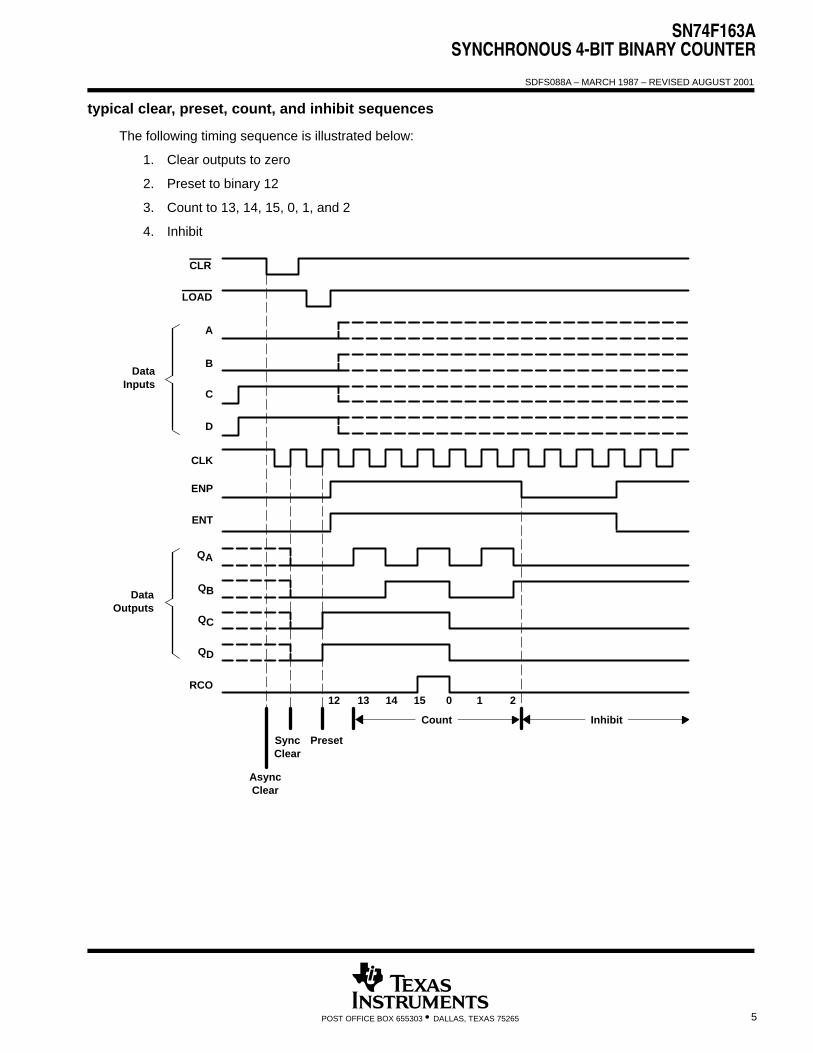
typical clear, preset, count, and inhibit sequences
The following timing sequence is illustrated below:
1. Clear outputs to zero
2. Preset to binary 12
3. Count to 13, 14, 15, 0, 1, and 2
4. Inhibit
DataInputs
DataOutputs
CLR
LOAD
A
B
C
D
CLK
ENP
ENT
RCO
QA
QB
QC
QD
AsyncClear
SyncClear
Preset
Count Inhibit
12 13 14 15 0 1 2
SN74F163ASYNCHRONOUS 4-BIT BINARY COUNTER
SDFS088A – MARCH 1987 – REVISED AUGUST 2001
6 POST OFFICE BOX 655303 • DALLAS, TEXAS 75265
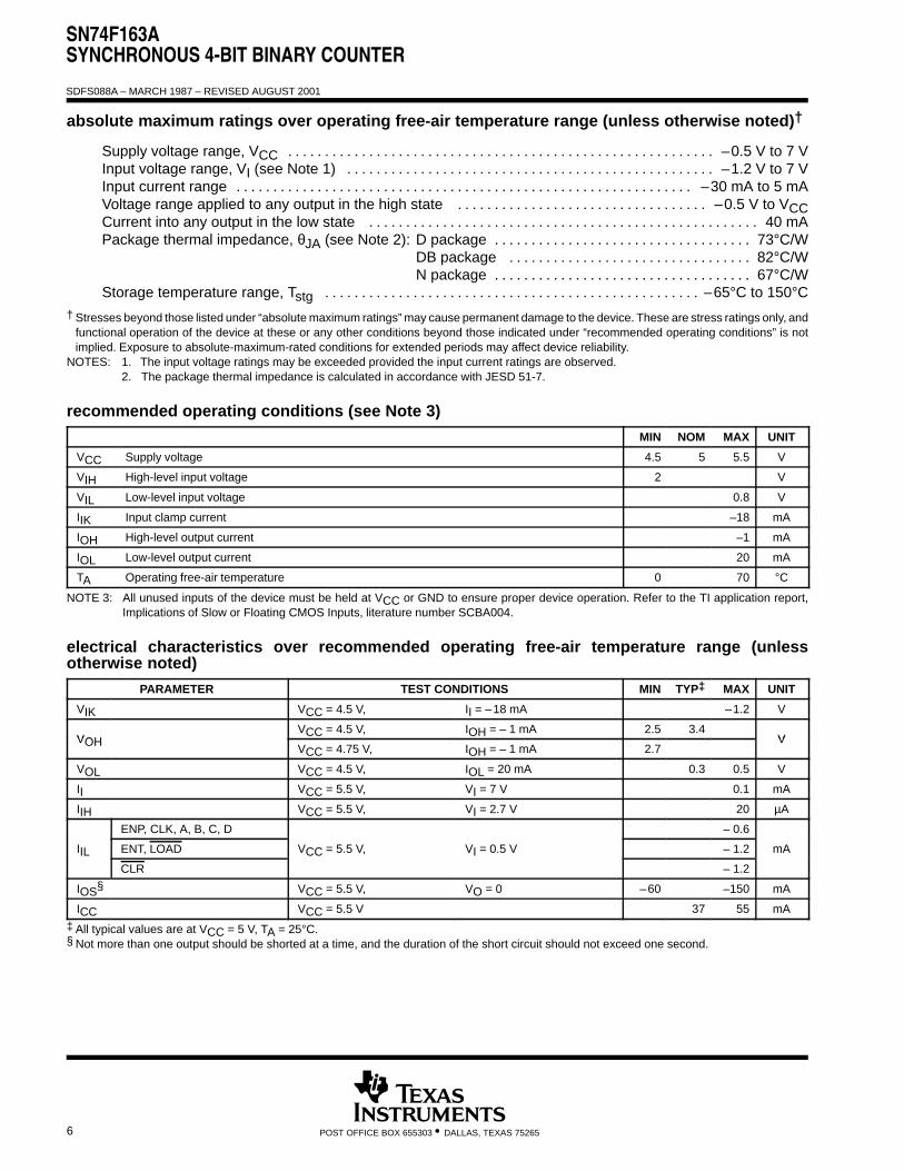
absolute maximum ratings over operating free-air temperature range (unless otherwise noted)†
Supply voltage range, VCC –0.5 V to 7 V. . . . . . . . . . . . . . . . . . . . . . . . . . . . . . . . . . . . . . . . . . . . . . . . . . . . . . . . . . Input voltage range, VI (see Note 1) –1.2 V to 7 V. . . . . . . . . . . . . . . . . . . . . . . . . . . . . . . . . . . . . . . . . . . . . . . . . . Input current range –30 mA to 5 mA. . . . . . . . . . . . . . . . . . . . . . . . . . . . . . . . . . . . . . . . . . . . . . . . . . . . . . . . . . . . . . Voltage range applied to any output in the high state –0.5 V to VCC. . . . . . . . . . . . . . . . . . . . . . . . . . . . . . . . . . Current into any output in the low state 40 mA. . . . . . . . . . . . . . . . . . . . . . . . . . . . . . . . . . . . . . . . . . . . . . . . . . . . . Package thermal impedance, θJA (see Note 2): D package 73°C/W. . . . . . . . . . . . . . . . . . . . . . . . . . . . . . . . . . .
DB package 82°C/W. . . . . . . . . . . . . . . . . . . . . . . . . . . . . . . . . N package 67°C/W. . . . . . . . . . . . . . . . . . . . . . . . . . . . . . . . . . .
Storage temperature range, Tstg –65°C to 150°C. . . . . . . . . . . . . . . . . . . . . . . . . . . . . . . . . . . . . . . . . . . . . . . . . . .
† Stresses beyond those listed under “absolute maximum ratings” may cause permanent damage to the device. These are stress ratings only, andfunctional operation of the device at these or any other conditions beyond those indicated under “recommended operating conditions” is notimplied. Exposure to absolute-maximum-rated conditions for extended periods may affect device reliability.
NOTES: 1. The input voltage ratings may be exceeded provided the input current ratings are observed.2. The package thermal impedance is calculated in accordance with JESD 51-7.
recommended operating conditions (see Note 3)
MIN NOM MAX UNIT
VCC Supply voltage 4.5 5 5.5 V
VIH High-level input voltage 2 V
VIL Low-level input voltage 0.8 V
IIK Input clamp current –18 mA
IOH High-level output current –1 mA
IOL Low-level output current 20 mA
TA Operating free-air temperature 0 70 °C
NOTE 3: All unused inputs of the device must be held at VCC or GND to ensure proper device operation. Refer to the TI application report,Implications of Slow or Floating CMOS Inputs, literature number SCBA004.
electrical characteristics over recommended operating free-air temperature range (unlessotherwise noted)
PARAMETER TEST CONDITIONS MIN TYP‡ MAX UNIT
VIK VCC = 4.5 V, II = –18 mA –1.2 V
VOHVCC = 4.5 V, IOH = – 1 mA 2.5 3.4
VVOHVCC = 4.75 V, IOH = – 1 mA 2.7
V
VOL VCC = 4.5 V, IOL = 20 mA 0.3 0.5 V
II VCC = 5.5 V, VI = 7 V 0.1 mA
IIH VCC = 5.5 V, VI = 2.7 V 20 µA
ENP, CLK, A, B, C, D – 0.6
IIL ENT, LOAD VCC = 5.5 V, VI = 0.5 V – 1.2 mA
CLR – 1.2
IOS§ VCC = 5.5 V, VO = 0 –60 –150 mA
ICC VCC = 5.5 V 37 55 mA
‡ All typical values are at VCC = 5 V, TA = 25°C.§ Not more than one output should be shorted at a time, and the duration of the short circuit should not exceed one second.
SN74F163ASYNCHRONOUS 4-BIT BINARY COUNTER
SDFS088A – MARCH 1987 – REVISED AUGUST 2001
7POST OFFICE BOX 655303 • DALLAS, TEXAS 75265
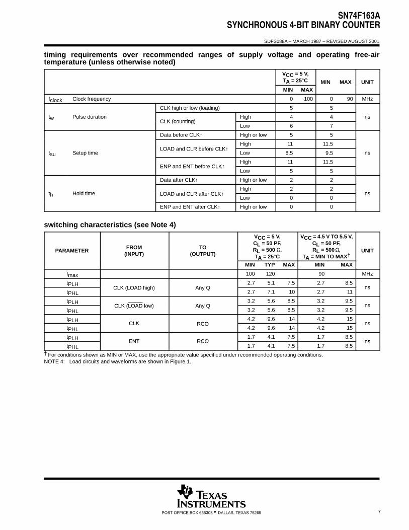
timing requirements over recommended ranges of supply voltage and operating free-airtemperature (unless otherwise noted)
VCC = 5 V,TA = 25°C MIN MAX UNITMIN MAX
fclock Clock frequency 0 100 0 90 MHz
CLK high or low (loading) 5 5
tw Pulse durationCLK (counting)
High 4 4 nsCLK (counting)
Low 6 7
Data before CLK↑ High or low 5 5
LOAD and CLR before CLK↑High 11 11.5
tsu Setup timeLOAD and CLR before CLK↑
Low 8.5 9.5 ns
ENP and ENT before CLK↑High 11 11.5
ENP and ENT before CLK↑Low 5 5
Data after CLK↑ High or low 2 2
th Hold time LOAD and CLR after CLK↑High 2 2
nsth Hold time LOAD and CLR after CLK↑Low 0 0
ns
ENP and ENT after CLK↑ High or low 0 0
switching characteristics (see Note 4)
PARAMETERFROM
(INPUT)TO
(OUTPUT)
VCC = 5 V,CL = 50 PF,RL = 500 Ω,TA = 25°C
VCC = 4.5 V TO 5.5 V,CL = 50 PF,RL = 500Ω,
TA = MIN TO MAX†UNIT
MIN TYP MAX MIN MAX
fmax 100 120 90 MHz
tPLHCLK (LOAD high) Any Q
2.7 5.1 7.5 2.7 8.5ns
tPHLCLK (LOAD high) Any Q
2.7 7.1 10 2.7 11ns
tPLHCLK (LOAD low) Any Q
3.2 5.6 8.5 3.2 9.5ns
tPHLCLK (LOAD low) Any Q
3.2 5.6 8.5 3.2 9.5ns
tPLHCLK RCO
4.2 9.6 14 4.2 15ns
tPHLCLK RCO
4.2 9.6 14 4.2 15ns
tPLH ENT RCO1.7 4.1 7.5 1.7 8.5
nstPHL
ENT RCO1.7 4.1 7.5 1.7 8.5
ns
† For conditions shown as MIN or MAX, use the appropriate value specified under recommended operating conditions.NOTE 4: Load circuits and waveforms are shown in Figure 1.
SN74F163ASYNCHRONOUS 4-BIT BINARY COUNTER
SDFS088A – MARCH 1987 – REVISED AUGUST 2001
8 POST OFFICE BOX 655303 • DALLAS, TEXAS 75265
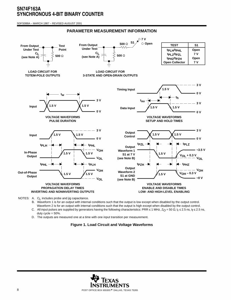
PARAMETER MEASUREMENT INFORMATION
3 V
3 V
0 V
0 V
thtsu
VOLTAGE WAVEFORMSSETUP AND HOLD TIMES
Data Input
tPLH
tPHL
tPHL
tPLH
VOH
VOH
VOL
VOL
3 V
0 VInput
Out-of-PhaseOutput
In-PhaseOutput
Timing Input
VOLTAGE WAVEFORMSPROPAGATION DELAY TIMES
INVERTING AND NONINVERTING OUTPUTS
OutputControl
OutputWaveform 1
S1 at 7 V(see Note B)
OutputWaveform 2
S1 at GND(see Note B)
VOL
VOH
tPZL
tPZH
tPLZ
tPHZ
≈3.5 V
0 V
VOL + 0.3 V
≈0 V
3 V
VOLTAGE WAVEFORMSENABLE AND DISABLE TIMES
LOW- AND HIGH-LEVEL ENABLING
tPLH/tPHLtPLZ/tPZLtPHZ/tPZH
Open Collector
Open7 V
Open7 V
TEST S1
3 V
0 V
tw
VOLTAGE WAVEFORMSPULSE DURATION
Input
NOTES: A. CL includes probe and jig capacitance.B. Waveform 1 is for an output with internal conditions such that the output is low except when disabled by the output control.
Waveform 2 is for an output with internal conditions such that the output is high except when disabled by the output control.C. All input pulses are supplied by generators having the following characteristics: PRR ≤ 1 MHz, ZO = 50 Ω, tr ≤ 2.5 ns, tf ≤ 2.5 ns,
duty cycle = 50%.D. The outputs are measured one at a time with one input transition per measurement.
From OutputUnder Test
CL(see Note A)
LOAD CIRCUIT FOR3-STATE AND OPEN-DRAIN OUTPUTS
S17 V
500 ΩFrom Output
Under TestCL
(see Note A)
TestPoint
LOAD CIRCUIT FORTOTEM-POLE OUTPUTS
Open
VOH – 0.3 V
500 Ω500 Ω
1.5 V 1.5 V
1.5 V 1.5 V
1.5 V 1.5 V
1.5 V 1.5 V
1.5 V1.5 V
1.5 V
1.5 V 1.5 V
1.5 V
1.5 V
Figure 1. Load Circuit and Voltage Waveforms
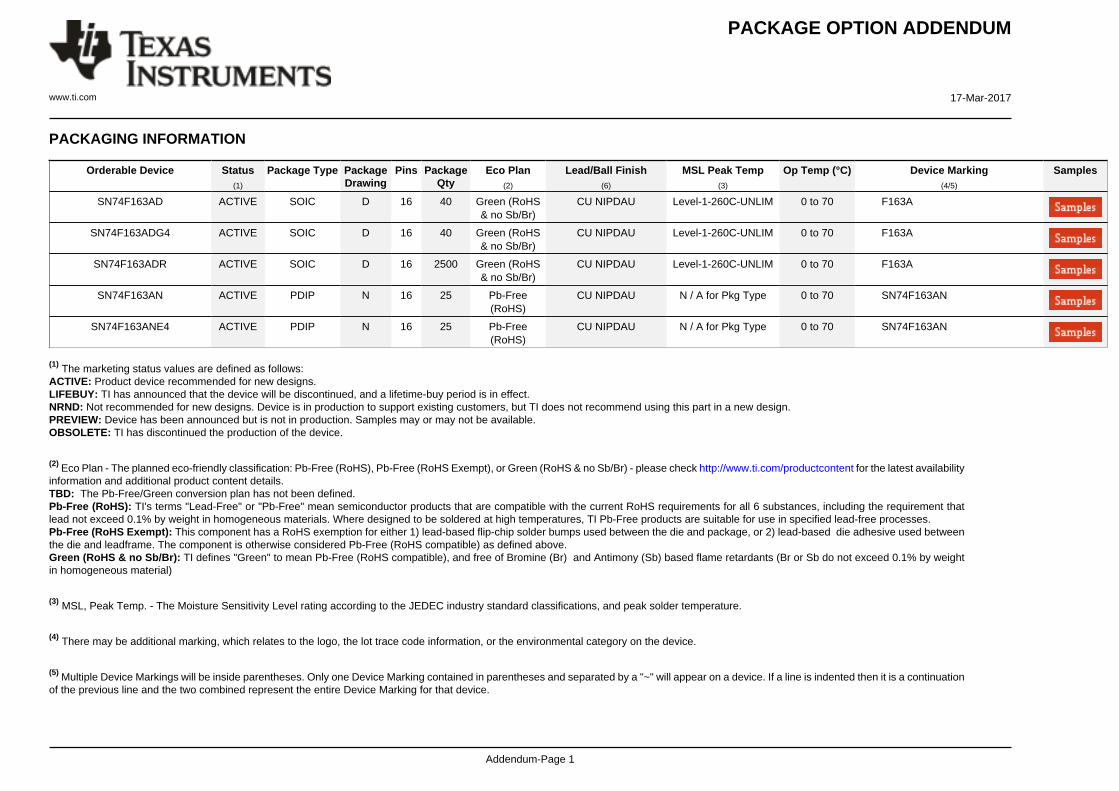
PACKAGE OPTION ADDENDUM
www.ti.com 17-Mar-2017
Addendum-Page 1
PACKAGING INFORMATION
Orderable Device Status(1)
Package Type PackageDrawing
Pins PackageQty
Eco Plan(2)
Lead/Ball Finish(6)
MSL Peak Temp(3)
Op Temp (°C) Device Marking(4/5)
Samples
SN74F163AD ACTIVE SOIC D 16 40 Green (RoHS& no Sb/Br)
CU NIPDAU Level-1-260C-UNLIM 0 to 70 F163A
SN74F163ADG4 ACTIVE SOIC D 16 40 Green (RoHS& no Sb/Br)
CU NIPDAU Level-1-260C-UNLIM 0 to 70 F163A
SN74F163ADR ACTIVE SOIC D 16 2500 Green (RoHS& no Sb/Br)
CU NIPDAU Level-1-260C-UNLIM 0 to 70 F163A
SN74F163AN ACTIVE PDIP N 16 25 Pb-Free(RoHS)
CU NIPDAU N / A for Pkg Type 0 to 70 SN74F163AN
SN74F163ANE4 ACTIVE PDIP N 16 25 Pb-Free(RoHS)
CU NIPDAU N / A for Pkg Type 0 to 70 SN74F163AN
(1) The marketing status values are defined as follows:ACTIVE: Product device recommended for new designs.LIFEBUY: TI has announced that the device will be discontinued, and a lifetime-buy period is in effect.NRND: Not recommended for new designs. Device is in production to support existing customers, but TI does not recommend using this part in a new design.PREVIEW: Device has been announced but is not in production. Samples may or may not be available.OBSOLETE: TI has discontinued the production of the device.
(2) Eco Plan - The planned eco-friendly classification: Pb-Free (RoHS), Pb-Free (RoHS Exempt), or Green (RoHS & no Sb/Br) - please check http://www.ti.com/productcontent for the latest availabilityinformation and additional product content details.TBD: The Pb-Free/Green conversion plan has not been defined.Pb-Free (RoHS): TI's terms "Lead-Free" or "Pb-Free" mean semiconductor products that are compatible with the current RoHS requirements for all 6 substances, including the requirement thatlead not exceed 0.1% by weight in homogeneous materials. Where designed to be soldered at high temperatures, TI Pb-Free products are suitable for use in specified lead-free processes.Pb-Free (RoHS Exempt): This component has a RoHS exemption for either 1) lead-based flip-chip solder bumps used between the die and package, or 2) lead-based die adhesive used betweenthe die and leadframe. The component is otherwise considered Pb-Free (RoHS compatible) as defined above.Green (RoHS & no Sb/Br): TI defines "Green" to mean Pb-Free (RoHS compatible), and free of Bromine (Br) and Antimony (Sb) based flame retardants (Br or Sb do not exceed 0.1% by weightin homogeneous material)
(3) MSL, Peak Temp. - The Moisture Sensitivity Level rating according to the JEDEC industry standard classifications, and peak solder temperature.
(4) There may be additional marking, which relates to the logo, the lot trace code information, or the environmental category on the device.
(5) Multiple Device Markings will be inside parentheses. Only one Device Marking contained in parentheses and separated by a "~" will appear on a device. If a line is indented then it is a continuationof the previous line and the two combined represent the entire Device Marking for that device.
PACKAGE OPTION ADDENDUM
www.ti.com 17-Mar-2017
Addendum-Page 2
(6) Lead/Ball Finish - Orderable Devices may have multiple material finish options. Finish options are separated by a vertical ruled line. Lead/Ball Finish values may wrap to two lines if the finishvalue exceeds the maximum column width.
Important Information and Disclaimer:The information provided on this page represents TI's knowledge and belief as of the date that it is provided. TI bases its knowledge and belief on informationprovided by third parties, and makes no representation or warranty as to the accuracy of such information. Efforts are underway to better integrate information from third parties. TI has taken andcontinues to take reasonable steps to provide representative and accurate information but may not have conducted destructive testing or chemical analysis on incoming materials and chemicals.TI and TI suppliers consider certain information to be proprietary, and thus CAS numbers and other limited information may not be available for release.
In no event shall TI's liability arising out of such information exceed the total purchase price of the TI part(s) at issue in this document sold by TI to Customer on an annual basis.
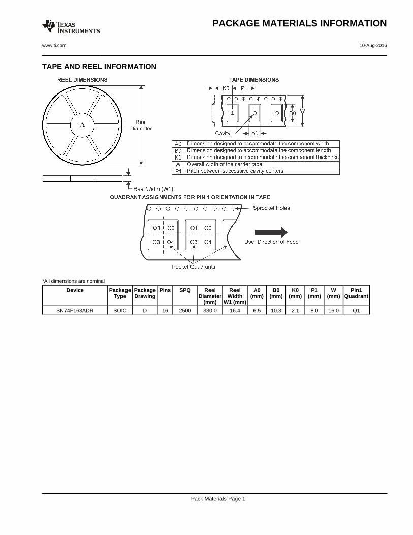
TAPE AND REEL INFORMATION
*All dimensions are nominal
Device PackageType
PackageDrawing
Pins SPQ ReelDiameter
(mm)
ReelWidth
W1 (mm)
A0(mm)
B0(mm)
K0(mm)
P1(mm)
W(mm)
Pin1Quadrant
SN74F163ADR SOIC D 16 2500 330.0 16.4 6.5 10.3 2.1 8.0 16.0 Q1
PACKAGE MATERIALS INFORMATION
www.ti.com 10-Aug-2016
Pack Materials-Page 1
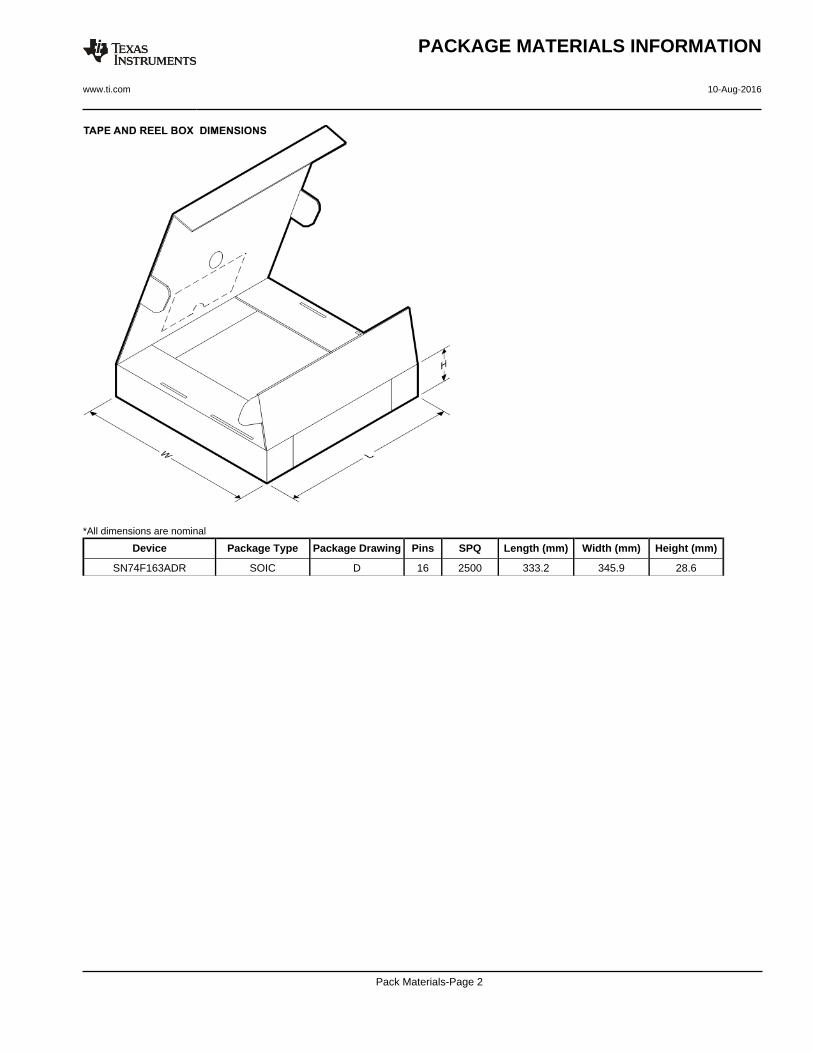
*All dimensions are nominal
Device Package Type Package Drawing Pins SPQ Length (mm) Width (mm) Height (mm)
SN74F163ADR SOIC D 16 2500 333.2 345.9 28.6
PACKAGE MATERIALS INFORMATION
www.ti.com 10-Aug-2016
Pack Materials-Page 2
IMPORTANT NOTICE
Texas Instruments Incorporated (TI) reserves the right to make corrections, enhancements, improvements and other changes to itssemiconductor products and services per JESD46, latest issue, and to discontinue any product or service per JESD48, latest issue. Buyersshould obtain the latest relevant information before placing orders and should verify that such information is current and complete.TI’s published terms of sale for semiconductor products (http://www.ti.com/sc/docs/stdterms.htm) apply to the sale of packaged integratedcircuit products that TI has qualified and released to market. Additional terms may apply to the use or sale of other types of TI products andservices.Reproduction of significant portions of TI information in TI data sheets is permissible only if reproduction is without alteration and isaccompanied by all associated warranties, conditions, limitations, and notices. TI is not responsible or liable for such reproduceddocumentation. Information of third parties may be subject to additional restrictions. Resale of TI products or services with statementsdifferent from or beyond the parameters stated by TI for that product or service voids all express and any implied warranties for theassociated TI product or service and is an unfair and deceptive business practice. TI is not responsible or liable for any such statements.Buyers and others who are developing systems that incorporate TI products (collectively, “Designers”) understand and agree that Designersremain responsible for using their independent analysis, evaluation and judgment in designing their applications and that Designers havefull and exclusive responsibility to assure the safety of Designers' applications and compliance of their applications (and of all TI productsused in or for Designers’ applications) with all applicable regulations, laws and other applicable requirements. Designer represents that, withrespect to their applications, Designer has all the necessary expertise to create and implement safeguards that (1) anticipate dangerousconsequences of failures, (2) monitor failures and their consequences, and (3) lessen the likelihood of failures that might cause harm andtake appropriate actions. Designer agrees that prior to using or distributing any applications that include TI products, Designer willthoroughly test such applications and the functionality of such TI products as used in such applications.TI’s provision of technical, application or other design advice, quality characterization, reliability data or other services or information,including, but not limited to, reference designs and materials relating to evaluation modules, (collectively, “TI Resources”) are intended toassist designers who are developing applications that incorporate TI products; by downloading, accessing or using TI Resources in anyway, Designer (individually or, if Designer is acting on behalf of a company, Designer’s company) agrees to use any particular TI Resourcesolely for this purpose and subject to the terms of this Notice.TI’s provision of TI Resources does not expand or otherwise alter TI’s applicable published warranties or warranty disclaimers for TIproducts, and no additional obligations or liabilities arise from TI providing such TI Resources. TI reserves the right to make corrections,enhancements, improvements and other changes to its TI Resources. TI has not conducted any testing other than that specificallydescribed in the published documentation for a particular TI Resource.Designer is authorized to use, copy and modify any individual TI Resource only in connection with the development of applications thatinclude the TI product(s) identified in such TI Resource. NO OTHER LICENSE, EXPRESS OR IMPLIED, BY ESTOPPEL OR OTHERWISETO ANY OTHER TI INTELLECTUAL PROPERTY RIGHT, AND NO LICENSE TO ANY TECHNOLOGY OR INTELLECTUAL PROPERTYRIGHT OF TI OR ANY THIRD PARTY IS GRANTED HEREIN, including but not limited to any patent right, copyright, mask work right, orother intellectual property right relating to any combination, machine, or process in which TI products or services are used. Informationregarding or referencing third-party products or services does not constitute a license to use such products or services, or a warranty orendorsement thereof. Use of TI Resources may require a license from a third party under the patents or other intellectual property of thethird party, or a license from TI under the patents or other intellectual property of TI.TI RESOURCES ARE PROVIDED “AS IS” AND WITH ALL FAULTS. TI DISCLAIMS ALL OTHER WARRANTIES ORREPRESENTATIONS, EXPRESS OR IMPLIED, REGARDING RESOURCES OR USE THEREOF, INCLUDING BUT NOT LIMITED TOACCURACY OR COMPLETENESS, TITLE, ANY EPIDEMIC FAILURE WARRANTY AND ANY IMPLIED WARRANTIES OFMERCHANTABILITY, FITNESS FOR A PARTICULAR PURPOSE, AND NON-INFRINGEMENT OF ANY THIRD PARTY INTELLECTUALPROPERTY RIGHTS. TI SHALL NOT BE LIABLE FOR AND SHALL NOT DEFEND OR INDEMNIFY DESIGNER AGAINST ANY CLAIM,INCLUDING BUT NOT LIMITED TO ANY INFRINGEMENT CLAIM THAT RELATES TO OR IS BASED ON ANY COMBINATION OFPRODUCTS EVEN IF DESCRIBED IN TI RESOURCES OR OTHERWISE. IN NO EVENT SHALL TI BE LIABLE FOR ANY ACTUAL,DIRECT, SPECIAL, COLLATERAL, INDIRECT, PUNITIVE, INCIDENTAL, CONSEQUENTIAL OR EXEMPLARY DAMAGES INCONNECTION WITH OR ARISING OUT OF TI RESOURCES OR USE THEREOF, AND REGARDLESS OF WHETHER TI HAS BEENADVISED OF THE POSSIBILITY OF SUCH DAMAGES.Unless TI has explicitly designated an individual product as meeting the requirements of a particular industry standard (e.g., ISO/TS 16949and ISO 26262), TI is not responsible for any failure to meet such industry standard requirements.Where TI specifically promotes products as facilitating functional safety or as compliant with industry functional safety standards, suchproducts are intended to help enable customers to design and create their own applications that meet applicable functional safety standardsand requirements. Using products in an application does not by itself establish any safety features in the application. Designers mustensure compliance with safety-related requirements and standards applicable to their applications. Designer may not use any TI products inlife-critical medical equipment unless authorized officers of the parties have executed a special contract specifically governing such use.Life-critical medical equipment is medical equipment where failure of such equipment would cause serious bodily injury or death (e.g., lifesupport, pacemakers, defibrillators, heart pumps, neurostimulators, and implantables). Such equipment includes, without limitation, allmedical devices identified by the U.S. Food and Drug Administration as Class III devices and equivalent classifications outside the U.S.TI may expressly designate certain products as completing a particular qualification (e.g., Q100, Military Grade, or Enhanced Product).Designers agree that it has the necessary expertise to select the product with the appropriate qualification designation for their applicationsand that proper product selection is at Designers’ own risk. Designers are solely responsible for compliance with all legal and regulatoryrequirements in connection with such selection.Designer will fully indemnify TI and its representatives against any damages, costs, losses, and/or liabilities arising out of Designer’s non-compliance with the terms and provisions of this Notice.
Mailing Address: Texas Instruments, Post Office Box 655303, Dallas, Texas 75265Copyright © 2017, Texas Instruments Incorporated