Embed Size (px)
Citation preview
Suresh RamalingamXilinx Inc.
IEEE CPMT, April 28, 2011
3D IC Development and Key Role of Supply Chain Collaboration
IEEE Components, Packaging, and ManufacturingTechnology Chapter, Santa Clara Valley
© Copyright 2010 Xilinx
Supply Chain Collaboration
Background and Motivation
Stacked Silicon Interconnect Technology
Agenda

Background and Motivation

© Copyright 2010 XilinxPage 4
Background: FPGA
High-Performance
6-LUT Fabric
High-Performance
6-LUT Fabric
36Kbit
Dual-Port
Block RAM / FIFO
with ECC
36Kbit
Dual-Port
Block RAM / FIFO
with ECC
SelectIO with
ChipSync
+ XCITE DCI
SelectIO with
ChipSync
+ XCITE DCI
550 MHz Clock
Management Tile
DCM + PLL
550 MHz Clock
Management Tile
DCM + PLL
25x18 Multiplier
DSP Slice with
Integrated ALU
25x18 Multiplier
DSP Slice with
Integrated ALU
More
Configuration
Options
More
Configuration
Options
Building Blocks– Configurable Logic Block (CLB)
• Configuration memory• Programmable switches• Interconnect drivers
– Hard IP (DSP, EMAC, etc.)– Block RAM– Configurable IOs– High-speed transceivers
Programmable SoC of logic, memory, and analog circuits

© Copyright 2010 Xilinx
Lower Power
Higher Bandwidth
Higher Capacity
Customers Are Asking for More
• More than 2X today’s logic capacity…
• Many more high-speed serial transceivers…
• Many more processing elements…
• Much more internal memory to store data…
Page 5

© Copyright 2010 Xilinx
FPGA Size
Early
Challenge 1: Availability and CapabilityLargest FPGAs only viable later in the life cycle
Yield
LaterSmaller
Page 6
© Copyright 2010 Xilinx
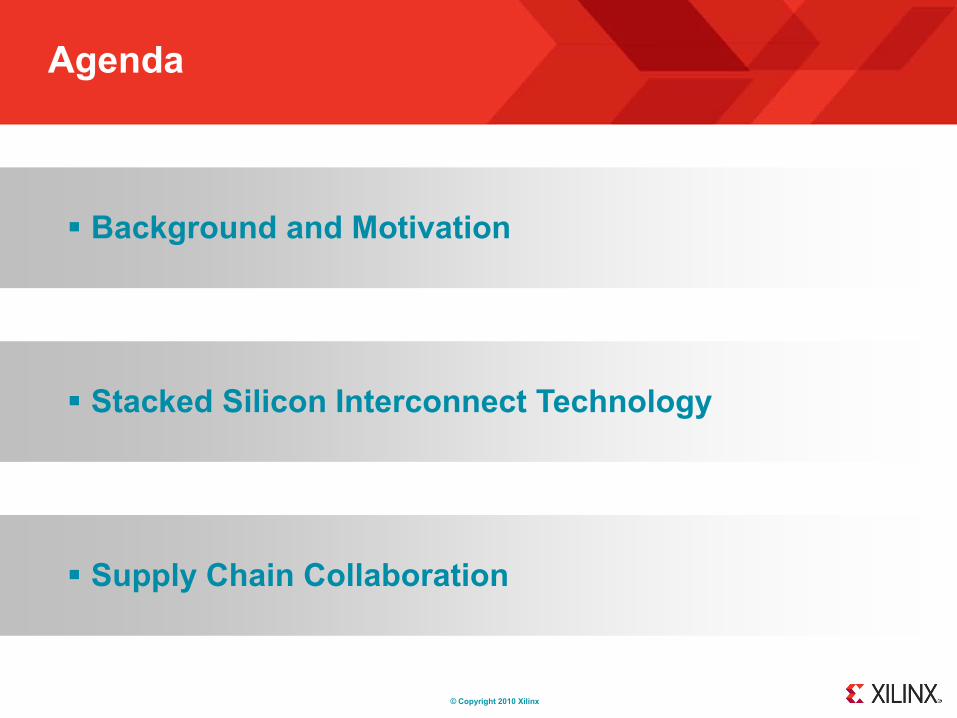
Challenge 2: Power and BandwidthTraditional mitigation techniques are no longer adequate
Large Monolithic FPGA Multiple FPGAs on PCB or MCM
Chip-to-Chip via Standard I/Os and SerDesMore total gates, sooner, but…
Resources Not Scaling1. Not enough I/Os2. I/O latencies too high3. Wasted I/O power
Innovation Needed
Page 7

© Copyright 2010 Xilinx
Introducing Stacked Silicon Interconnect TechnologyHigh Bandwidth, Low Latency, Low Power
Large Monolithic FPGA
Xilinx Innovation
Massive number of low latency, die-to-die connections Earlier in time No wasted I/O power Over five years of R&D
Multiple chips on PCB or MCB
Delivers the Best of Both Worlds: High and Usable Capacity
I/O performance bottlenecks & power
Page 8

© Copyright 2010 Xilinx
Delivers Resource-Rich FPGAs
Largest Device with Transceivers
Logi
c C
ells
3.5x 1.9x
Page 9
2M logic density enabled one
generation ahead!

© Copyright 2010 Xilinx
High PerformanceComputing
Next Gen Wireless Communications
For the Most Demanding FPGA Applications
Next Gen Wired Communications
Aerospace & Defense
MedicalImaging
Page 10
Industry’s HighestSystem Performance
and Capacity

© Copyright 2010 XilinxPage 11
Summary
SSIT Addresses IO Bottleneck 100X better BW/W over traditional IOs/SerDes
Can offer Next Generation Density Now
SSIT Platform Enables – Optimal Partitioning
• Digital and analog blocks• IP/IC reuse
– Heterogeneous Integration• Digital, mixed signal, & optical• FPGA & memory

© Copyright 2010 Xilinx
Summary
Technology Overview
Supply Chain Collaboration
Stacked Silicon Interconnect Technology

© Copyright 2010 Xilinx
Xilinx FPGA Architectural InnovationsAt the Heart of the Technology
ASMBL Optimized FPGAslice
FPGA Slices Side-by-Side
Silicon Interposer
Silicon Interposer:>10K routing connections between slices~1ns latency
Page 13

© Copyright 2010 Xilinx
Silicon Interposer
Microbumps
Through-Silicon Vias
Page 14
Harnesses Proven Technology in a Unique Way
Package Substrate
28nm FPGA Slice 28nm FPGA Slice28nm FPGA Slice28nm FPGA Slice
C4 Bumps
BGA Balls
Microbumps• Access to power / ground / IOs• Access to logic regions• Leverages ubiquitous image sensor
micro-bump technologyThrough-silicon Vias (TSV)• Only bridge power / ground / IOs to C4 bumps• Coarse pitch, low density aids manufacturability• Etch process (not laser drilled)
Side-by-Side Die Layout• Minimal heat flux issues• Minimal design tool flow impact
Passive Silicon Interposer (65nm Generation)• 4 conventional metal layers connect micro bumps & TSVs• No transistors means low risk and no TSV induced
performance degradation
New!

© Copyright 2010 XilinxPage 15
Virtex-7 SSIT uses 28 nm FPGA and 65 nm Interposer
Low risk approach to integrate TSV & u-bump– Passive silicon interposer with 65nm interconnects & coarse-pitch TSV
High density micro-bump for 10K-30K chip-to-chip connections Better FPGA low-k stress management with silicon interposer
Technology SpecsM1-M4 2um pitch 4 4X layers
TSV >10 um diameter & 210um pitch
Micro-bump 45um pitch
C4 210um pitch
Package 4-2-4 Layer, 1.0 mm BGA pitch
Micro-bump TSV Interposer
Substrate
Courtesy of Xilinx, TSMC, Amkor
28nm Test Vehicle + 65 nm Interposer

© Copyright 2010 Xilinx
Correlation between Measurement and Simulation
Insertion Loss S21 [dB] Return Loss S11 [dB]
Dotted Red Trace – MeasurementSolid Blue Trace - Simulation
Through transmission structure using two TSVs

© Copyright 2010 XilinxPage 18
Eyes After TSV Optimization
w/o Interposerw/ Interposer
10Gbps 13Gbps

© Copyright 2010 Xilinx
Reliability Validation Status
Reliability Tests Focus Areas ResultsPackage Level L4 Precon and TCB TSV and C4 Passed 1000 TCB
Wafer Level TCB TSV& Interposer Interconnects Passed 1000 TCB
Electro-migration Micro-bump Joint Passed 0.1% CDF for 10 years
High Temperature Storage Micro-bump Joint Passed 1000 hours
Package Level L4 Precon and TCB – 1st Leg
Micro-bump Joint, TSV, C4 Interconnects Passed L4 and 500 TCB (CSAM)
Package Level L4 Precon and TCB – 2st Leg
Micro-bump Joint, TSV, C4 Interconnects In progress
Package TechnologyQualification- L4 Precon, TCB, THB, HTOL, HTS
Micro-bump Joint, TSV, C4, Silicon, Package In planning
Page 19

© Copyright 2010 Xilinx
Underfill
Initial Underfill MRT L5/250
HAST 48 Hours HAST 264 Hours
No Delamination, Post HAST: 110C, 85% RH, 264 HoursCourtesy of Xilinx, TSMC, Amkor

© Copyright 2010 XilinxPage 21
Establishing a Supply Chain Flow
Wafer with TSVC4 bump, Probe
Carrier
Carrier MountThin & TSV Reveal
RDL & u-bump
Carrier De-mountTo Film Frame
Die-to-Substrate Die-to-Wafer
3D-Package Assembly
Wafer with TSVC4 bump, Probe
Carrier
Carrier MountThin & TSV Reveal
RDL & u-bumpDie-to-wafer
DiceDice
Page 21
Considerations Product and Cost Requirements Scalable Business Model Design Rules (Foundry vs. OSAT) Heterogeneous Die integration
© Copyright 2010 Xilinx
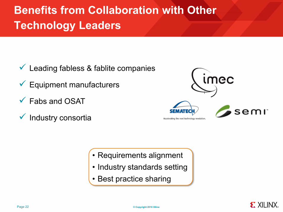
Benefits from Collaboration with Other Technology Leaders
• Requirements alignment• Industry standards setting• Best practice sharing
Leading fabless & fablite companies
Equipment manufacturers
Fabs and OSAT
Industry consortia
Page 22

© Copyright 2010 Xilinx
Xilinx has a Robust Supply Chain
Leading foundry and OSAT partners
Package Substrate 28nm FPGA & Interposer
Bump, Die separationCoC attach, & Assembly
Final Test of Packaged Part
IBIDEN
FPGA, Interposer, & Package Design

© Copyright 2010 XilinxPage 24
TSMC Discusses Stacked Silicon Interconnect
Page 24
Dr. Shang-Yi ChiangSenior Vice President, R&D, TSMC
TSMC Presentation
© Copyright 2010 Xilinx
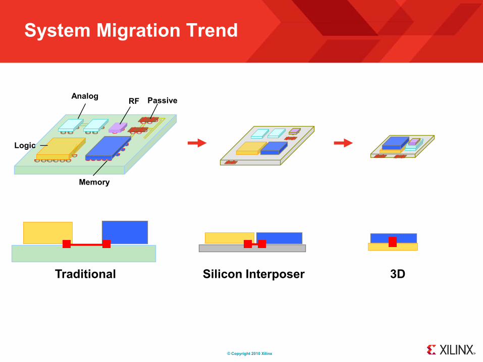
System Migration Trend
Analog
Logic
RF Passive
Memory
Silicon Interposer 3DTraditional

© Copyright 2010 Xilinx
Xilinx Is Well on the Way to Volume Production
Test Vehicle CY09 CY10 CY11 CY12
TV1 (90nm)
TV2 (40nm)
TV3 (28nm)
Device (28nm)
Page 26
Module DevelopmentProcess IntegrationReliability AssessmentSupply Chain Validation
Design Enablement
Design ValidationProcess Qualification
Initial Sampling
Today
EA Design ToolsISE 13.1 Beta ES ProdTO
© Copyright 2010 Xilinx
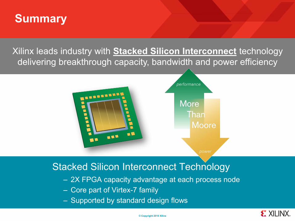
Summary
Stacked Silicon Interconnect Technology– 2X FPGA capacity advantage at each process node– Core part of Virtex-7 family– Supported by standard design flows
Xilinx leads industry with Stacked Silicon Interconnect technology delivering breakthrough capacity, bandwidth and power efficiency