Embed Size (px)
Citation preview

Networks-on-Chip in a Three-DimensionalEnvironment: A Performance Evaluation
Brett Stanley Feero, Member, IEEE, and Partha Pratim Pande, Member, IEEE
Abstract—The Network-on-Chip (NoC) paradigm has emerged as a revolutionary methodology for integrating a very high number ofintellectual property (IP) blocks in a single die. The achievable performance benefit arising out of adopting NoCs is constrained by theperformance limitation imposed by the metal wire, which is the physical realization of communication channels. With technologyscaling, only depending on the material innovation will extend the lifetime of conventional interconnect systems a few technologygenerations. According to the International Technology Roadmap for Semiconductors (ITRS) for the longer term, new interconnectparadigms are in need. The conventional 2D integrated circuit (IC) has limited floorplanning choices, and consequently, it limits theperformance enhancements arising out of NoC architectures. Three-dimensional ICs are capable of achieving better performance,functionality, and packaging density compared to more traditional planar ICs. On the other hand, NoC is an enabling solution forintegrating large numbers of embedded cores in a single die. Three-dimensional NoC architectures combine the benefits of these twonew domains to offer an unprecedented performance gain. In this paper, we evaluate the performance of 3D NoC architectures anddemonstrate their superior functionality in terms of throughput, latency, energy dissipation, and wiring area overhead compared totraditional 2D implementations.
Index Terms—Network-on-chip, 3D integrated circuits, throughput, latency, energy, area, wormhole routing.
Ç
1 INTRODUCTION
WITH shrinking geometries, global interconnects arebecoming the principal performance bottleneck for
high-performance Systems-on-Chip (SoCs) [1], [2], [3]. Theselong interconnects are quickly becoming a performanceimpediment in terms of communication latency and power[4]. The Network-on-Chip (NoC) model is emerging as arevolutionary methodology in solving the performancelimitations arising out of long interconnects, outperformingmore mainstream bus architectures [5], [6]. In addition toproviding a solution for the global wire delay problem, theNoC paradigm also eases integration of high numbers ofintellectual property (IP) cores in a single SoC. However,restricted floorplanning choices of the 2D integrated circuits(ICs) limit the performance enhancements arising out ofNoC architectures. As shown in Fig. 1, 3D ICs, which containmultiple layers of active devices, have the potential forenhancing system performance [7], [8], [9], [10]. Accordingto [7], 3D ICs allow for performance enhancements even inthe absence of scaling. This is the result of the reduction ininterconnect length. Besides this clear benefit, packagedensity is increased significantly, power is reduced fromshorter wires, and circuitry is more immune to noise [7]. Theperformance improvement arising from the architecturaladvantages of NoCs will be significantly enhanced if 3D ICsare adopted as the basic fabrication methodology. Theamalgamation of two emerging paradigms, NoC and 3D IC,allows for the creation of new structures that enable
significant performance enhancements over more tradi-tional solutions. With freedom in the third dimension,architectures that were impossible or prohibitive due towiring constraints in planar ICs are now possible, and many3D implementations can outperform their 2D counterparts.
In this paper, we characterize the performance of multiple3D NoC architectures in the presence of realistic trafficpatterns through cycle-accurate simulation and establish theperformance benchmark and related design trade-offs.
This paper is organized as follows: Section 2 coversprevious research and developments pertinent to this study.Section 3 is an introduction to the different 3D NoCarchitectures evaluated in this paper. Section 4 reviewsthe performance metrics used to evaluate the networkarchitectures. Section 5 details the experimental analysis,and finally, Section 6 concludes this paper.
2 RELATED WORK
Current SoCs are implemented predominantly following2D architectures. However, the emergence of 3D ICs willpresent a fundamental change. Topol et al. [7] describe, indetail, the challenges of manufacturing in a 3D IC process. Itshows that 3D ICs are capable of improvements in power,noise, logical span, density, performance, and functionality.One major advantage of the 3D IC paradigm is that it allowsfor the integration of “dissimilar technologies,” e.g.,memory, analog, MEMS, and so forth, in a single die. Thispaper describes the benefits and drawbacks of differentfabrication methods including face-to-face bonding andface-to-back bonding. With an SOI face-to-back process, thevia pitch is minimized, at 0.4 �m with a separation of 2 �mbetween layers of SOI devices [7].
Jacob et al. [11] propose using 3D ICs to improve theperformance of microprocessors by forming a processor-memory stack. They show that the integration of processor
32 IEEE TRANSACTIONS ON COMPUTERS, VOL. 58, NO. 1, JANUARY 2009
. B.S. Feero is with ARM Ltd., 110 Fulbourn Road, Cambridge CB2 0NU,UK. E-mail: [email protected].
. P.P. Pande is with the School of Electrical Engineering and ComputerScience, Washington State University, PO Box 642752, Pullman,WA 99164-2752. E-mail: [email protected].
Manuscript received 26 June 2007; revised 21 Feb. 2008; accepted 20 May2008; published online 6 Aug. 2008.Recommended for acceptance by F. Lombardi.For information on obtaining reprints of this article, please send e-mail to:[email protected], and reference IEEECS Log Number TC-2007-06-0260.
0018-9340/09/$25.00 � 2009 IEEE Published by the IEEE Computer Society
Authorized licensed use limited to: Washington State University. Downloaded on June 16,2010 at 22:16:56 UTC from IEEE Xplore. Restrictions apply.

and memory in a stack enables a large increase inperformance. In particular, 3D integration enables the useof very wide buses (> 1,024 bits) for vertical communica-tion. In addition to ultrawide buses, a stack provides a veryshort distance between the processor and memory, decreas-ing memory access times considerably.
In [12], 3D ICs were proposed to improve performance ofchip multiprocessors. Drawing upon 3D IC research, theychose a hybridization of buses and networks to provide theinterconnect fabric between CPUs and L2 caches. Theperformance of this fusion of NoC and bus architectureswas evaluated using standard CPU benchmarks. However,this analysis pertains only to chip multiprocessors anddoes not consider the use of 3D network structures forapplication-specific SoCs. Three-dimensional NoCs areanalyzed in terms of temperature in [13]. Pavlidis andFriedman [14] compared 2D MESH structures with their 3Dcounterparts by analyzing the zero-load latency and powerconsumption of each network. This is an evaluation thatshows some of the advantages of 3D NoCs, but it neitherapplies any real traffic pattern nor does it measure otherrelevant performance metrics. We aim to address these
concerns by applying real traffic patterns in a cycle-accuratesimulation and by measuring performance through estab-lished metrics for 3D NoC structures.
3 3D NOC ARCHITECTURES
Enabling design in the vertical dimension permits a largedegree of freedom in choosing an on-chip networktopology. Due to wire-length constraints and layoutcomplications, the more conventional 2D ICs have placedlimitations on the types of network structures that arepossible. With the advent of 3D ICs, a wide range of on-chipnetwork structures that were not explored earlier are beingconsidered [12], [14]. This paper investigates five differenttopologies in 3D space and compares them with three well-known NoC architectures from 2D implementations. Weconsider a SoC with a 400-mm2 floorplan and 64 functionalIP blocks. We selected this system size to reflect the state ofthe art of emerging SoCs. At ISSCC 2007, the design of an80-core processor arranged in an 8 � 10 regular grid builton fundamental NoC concepts was demonstrated [15].Therefore, we believe that the system size assumed in thiswork is representative of the current trends. IP blocks for3D SoC are mapped onto four 10 mm � 10 mm layers,in order to occupy the same total area as a single-layer,20 mm � 20 mm layout.
3.1 Mesh-Based Networks
One of the well-known 2D NoC architectures is the 2D Mesh,as shown in Fig. 2a. This architecture consists of an m� nmesh of switches interconnecting IP blocks placed alongwith them. It is known for its regular structure andshort interswitch wires. From this structure, a variety of3D topologies can be derived. The straightforward extensionof this popular planar structure is the 3D Mesh. Fig. 2b showsan example of 3D Mesh-based NoC. It employs seven-port
FEERO AND PANDE: NETWORKS-ON-CHIP IN A THREE-DIMENSIONAL ENVIRONMENT: A PERFORMANCE EVALUATION 33
Fig. 1. Three-dimensional IC from an SOI process.
Fig. 2. Mesh-based NoC architectures. (a) Two-dimensional mesh. (b) Three-dimensional mesh. (c) Stacked mesh. (d) Ciliated 3D mesh.
Authorized licensed use limited to: Washington State University. Downloaded on June 16,2010 at 22:16:56 UTC from IEEE Xplore. Restrictions apply.

switches: one port to the IP block, one each to switches aboveand below, and one in each cardinal direction (North, South,East, and West), as shown in Fig. 3a.
A second derivation, Stacked Mesh (Fig. 2c), takesadvantage of the short interlayer distances that arecharacteristics of a 3D IC, which can be around 20 �m [7].Stacked Mesh is a hybrid between a packet-switchednetwork and a bus. It integrates multiple layers of 2D Meshnetworks by connecting them with a bus spanning theentire vertical distance of the chip. As the distance betweenthe individual 2D layers in 3D IC is extremely small, theoverall length of the bus is also small, making it a suitablechoice for communicating in the z-dimension [12]. Further-more, each bus has only a small number of nodes (i.e., equalto the number of layers of silicon), keeping the overallcapacitance on the bus small and greatly simplifying busarbitration. For consistency with [12], our analysis considersthe use of a dynamic, time-division multiple-access(dTDMA) bus, although any other type of bus may be usedas well. A switch in a Stacked Mesh network has, at most,six ports: one to the IP, one to the bus, and four for thecardinal directions (Fig. 3b). Additionally, it is possible toutilize ultrawide buses similar to the approach introducedin [11] to implement cost-effective, high-bandwidth com-munication between layers.
A third method of constructing a 3D NoC is by addinglayers of functional IP blocks and restricting the switches toone layer or a small number of layers. With this in mind, weintroduce a new architecture, ciliated 3D Mesh. Thisstructure is essentially a 3D Mesh network with multipleIP blocks per switch. For the ciliated 3D Mesh, we considera 4 � 4 � 2 3D Mesh network with two IPs per switch,where the two functional IP blocks occupy, more or less, thesame footprint but reside at different layers. This is shownin Fig. 2d. In a ciliated 3D Mesh network, each switchcontains seven ports (one for each cardinal direction, oneeither up or down, and one to each of the two IP blocks), asshown in Fig. 3c. This architecture will clearly exhibit loweroverall bandwidth than a complete 3D Mesh due tomultiple IP blocks per switch and reduced connectivity;however, we will show that this type of network offers anadvantage in terms of energy dissipation, especially in thepresence of specific traffic patterns.
It is important to note that each mesh-based networkintroduced in this section can be easily translated into atoroidal structure.
3.2 Tree-Based Networks
Two types of tree-based interconnection networks that havebeen considered for NoC applications are butterfly fat tree(BFT) [16], [17] and the generic fat tree, or SPIN [18]. Thispaper endeavors to quantify the enhancements achievedwhen these networks are instantiated in a 3D IC environ-ment. Unlike the work with mesh-based NoCs, we do notpropose any new topologies for tree-based systems. Instead,we investigate the achievable performance benefits byinstantiating already-existing tree-based NoC topologies ina 3D environment.
The BFT topology we consider is shown in Fig. 4a. For a64-IP SoC, a BFT network will contain 28 switches. Eachswitch (Fig. 5a) in a BFT network consists of six ports, one toeach of four child nodes and two to parent nodes, with theexception of the switches at the topmost layer. Whenmapped to a 2D structure, the longest interswitch wirelength for a BFT-based NoC is l2DIC=2, where l2DIC is thedie length on one side [17], [5]. If the NoC is spread over a20 mm � 20 mm die, then the longest interswitch wire is10 mm [5], as shown in Fig. 4c. Yet, when the same BFTnetwork is mapped onto a four-layer 3D SoC, wire routingbecomes simpler, and the longest interswitch wire length isreduced by at least a factor of two, as can be seen in Fig. 4d.This will lead to reduced energy dissipation as well as lessarea overhead. The fat tree topology in Fig. 4b will have thesame advantages when mapped on to a 3D IC as the BFT.
4 PERFORMANCE ANALYSIS AND DESIGN COST
In order to properly analyze the various 3D NoC topologies,a standard set of metrics must be used [19]. We assumewormhole routing [20] as the data transport mechanismwhere the packet is divided into fixed length flow controlunits or flits. The header flit holds the routing and controlinformation. It establishes a path, and subsequent payloador body flits follow that path. Our comparative analysisfocuses on the four established benchmarks [19] ofthroughput, latency, energy, and area overhead.
Throughput is a metric that quantifies the rate in whichmessage traffic can be sent across a communication fabric. Itis defined as the average number of flits arriving per IPblock per clock cycle, so the maximum throughput of asystem is directly related to the peak data rate that a systemcan sustain. Accordingly, it is important to note that athroughput of 1 corresponds to every node accepting oneflit in every clock cycle.
34 IEEE TRANSACTIONS ON COMPUTERS, VOL. 58, NO. 1, JANUARY 2009
Fig. 3. Switches for mesh-based NoCs. (a) Three-dimensional mesh. (b) Stacked mesh. (c) Ciliated 3D mesh.
Authorized licensed use limited to: Washington State University. Downloaded on June 16,2010 at 22:16:56 UTC from IEEE Xplore. Restrictions apply.

Next, latency refers to the length of time elapsed betweenthe injection of a message header at the source node and thereception of the tail flit at the destination.
The transport of messages across a network leads to aquantifiable amount of energy dissipation. Activity in thelogic gates of the network switches as well as the chargingand discharging of interconnection wires lead to theconsumption of energy.
Last, the amount of silicon area used by an interconnec-tion network is a necessary consideration. Networkswitches, layer-to-layer vias, interswitch wires, and buffersincurred by relatively longer wires all use a certain amountof area of the chip.
4.1 Performance Analysis in 3D Mesh-Based NoCs
In this section, we analyze the performance of the 3DMesh-based NoC architectures in terms of the parametersmentioned above.
Throughput is given in the number of accepted flits perIP per cycle. This metric, therefore, is closely related to themaximum amount of sustainable traffic in a certainnetwork type. Any improvements in throughput in 3Dnetworks are principally related to two factors: thenumber of physical links and the average number of hops.
In general, for a Mesh-based NoC, the number of links isgiven as follows:
links ¼ N1N2ðN3 � 1Þ þN1N3ðN2 � 1Þ þN2N3ðN1 � 1Þ;ð1Þ
where Ni represents the number of switches in theith dimension. For instance, in an 8 � 8 2D Mesh-basedNoC, this yield 112 links. In a 4 � 4 � 4 3D Mesh-basedNoC, the number of links turns out to be 144. With a greaternumber of links, a 3D Mesh network, for example, is able tocontain a greater number of flits and therefore transmit agreater number of messages.
However, only considering the number of links will notcharacterize the overall throughput of a network. Theaverage hop count also has a definitive effect on throughput.Following [14], the average number of hops in a mesh-basedNoC is given by
hopsNoC ¼n1n2n3ðn1 þ n2 þ n3Þ � n3ðn1 þ n2Þ � n1n2
3ðn1n2n3 � 1Þ ; ð2Þ
where ni is the number of nodes in the ith dimension.This equation applies both to the 4 � 4 � 4 3D Mesh and
FEERO AND PANDE: NETWORKS-ON-CHIP IN A THREE-DIMENSIONAL ENVIRONMENT: A PERFORMANCE EVALUATION 35
Fig. 4. Tree architectures. (a) BFT. (b) SPIN. (c) Two-dimensional BFT floorplan. (d) Three-dimensional BFT floorplan for the first two layers.(e) The first three layers of a 3D BFT floorplan as seen in elevation view.
Fig. 5. Switches for tree networks. (a) BFT. (b) SPIN.
Authorized licensed use limited to: Washington State University. Downloaded on June 16,2010 at 22:16:56 UTC from IEEE Xplore. Restrictions apply.

4 � 4 � 2 ciliated 3D Mesh networks. The number ofhops for the Stacked Mesh is equal to
hopsStacked ¼n1 þ n2
3þ n3 � 1
n3: ð3Þ
For our 4 � 4 � 4 3D Mesh and 8 � 8 2D Mesh, averagehop counts are 3.81 and 5.33, respectively. There are40 percent more hops in the 2D Mesh compared to that inthe 3D Mesh. Consequently, flits in 3D Mesh needs totraverse less number of stages between a pair of source anddestination than the 2D counterpart. As a result of this, weexpect a corresponding increase in throughput. A loweraverage hop count will also allow more flits to be transmittedthrough the network. With a lower hop count, a wormhole-routed packet will utilize fewer links, thus leaving moreroom to increase the maximum sustainable traffic.
Transport latency, like throughput, is also affected byaverage hop count. It is also affected heavily by the numberof links and the injection load. In 3D architectures, adecrease in latency is expected due to a lower hop countand an increased number of links.
In the SoC realm, energy dissipation characteristics of theinterconnect structures are crucial, as the interconnect fabriccan consume a significant portion of the overall energybudget [13]. The energy dissipation in an NoC depends onthe energy dissipated by the switch blocks and theinterswitch wire segments. Both of these factors dependon the network architecture. Additionally, the injection loadhas a significant contribution as it is the cause for anyactivity in the switches and interswitch wires. Intuitively, itis clear that with more packets traversing the network,power will increase. This is why packet energy is animportant attribute for characterizing NoC structures. Theenergy dissipated per flit per hop is given by
Ehop ¼ Eswitch þ Ewire; ð4Þ
where Eswitch and Ewire are the energy dissipated by eachswitch and interswitch wire segments, respectively. Theenergy of a packet of length n flits that completes h hops isgiven by
Epacket ¼ nXhj¼1
Ehop;j: ð5Þ
From this, a formula for packet energy can be realized. IfP packets are transmitted, then the average energydissipated per packet is given as
Epacket ¼
PPi¼1
Epacket;i
P¼
PPi¼1
niPhij¼1
Ehop;j
!
P: ð6Þ
Now, it is clear that a strong correlation exists betweenpacket energy and the number of hops from source todestination. Consequently, a network topology that exhibitssmaller hop counts will also exhibit correspondingly lowerpacket energy. As all 3D mesh-based NoC architecturesexhibit a lower hop count, they should also dissipate lessenergy per packet.
Last, the area overhead must be analyzed for mesh-basedNoCs. Area overhead for an NoC includes switch overhead
and wiring overhead. Switch area is affected by the overallnumber of switches and the area per switch, which is highlycorrelated to the number of ports. Since all 3D mesh-basedNoCs have more ports, the area per switch will increase.However, the ciliated structure has a reduced number ofswitches, which should significantly reduce the overallswitch area. For 3D NoCs in general, wiring overheadincludes the interlayer via footprint in addition to the areaincurred by horizontal and vertical wirings. The addition ofinterlayer vias and their corresponding area overhead is acharacteristic that is unique to 3D ICs, and it is included inthe area overhead calculations presented in Section 5.
Wire overhead is reduced when moving to a 3D IC.However, this is not due to reductions in the length of mostinterswitch wires. Horizontal wire length is given bylIC=nside, where nside represents the number of IPs in onedimension of the IC and lIC is the die length on one side, asshown in Figs. 2a and 2b. For the 8 � 8 2D Mesh, thisevaluates to 20 mm/8 or 2.5 mm, and for all 3D mesh-basedarchitectures, the expression evaluates to 10 mm/4, also2.5 mm. With this in mind, reductions in wire overheadcome from the interlayer wires. The 3D structures have areduced number of horizontal links due to the presence ofinterlayer wires. These interlayer wires are very small, andhence, they are the source of wire overhead savings inmesh-based 3D NoCs.
4.2 Performance Analysis in 3D Tree-Based NoCs
Unlike the previous discussion pertaining to mesh-basedNoCs, the tree-based networks we consider for 3Dimplementations have identical topologies to their 2Dcounterparts. The only variable is the interswitch wirelength. As a result, there are significant improvements bothin terms of energy and area overhead.
In 2D space, the longest interswitch wire length in a BFTor SPIN network is equal to l2DIC=2 [17], [5], where l2DIC isthe die length on one side. This interswitch wire lengthcorresponds to the topmost level of the tree. In a 3D IC,however, this changes significantly. For instance, as shownin Figs. 4d and 4e, the longest wire length for 3D, tree-basedNoC is equal to the length of the horizontal travel inaddition to the length of the vertical via. Considering a20 mm � 20 mm 2D die, the longest interswitch wire lengthis equal to 10 mm, whereas with a 10 mm � 10 mm stack offour layers, the maximum wire length is equal to the sum ofl3DIC=4, or 2.5 mm, and the span of two layers, 40 �m. Thisis almost a factor-of-four reduction compared to 2Dimplementations. Similarly, mid-level wire lengths arereduced by a factor of 2. As a result, this reduction in wirelength, shown in Table 1, causes a significant reduction inenergy.
36 IEEE TRANSACTIONS ON COMPUTERS, VOL. 58, NO. 1, JANUARY 2009
TABLE 1Interswitch Wire Lengths in 3D Tree-Based NoCs
Authorized licensed use limited to: Washington State University. Downloaded on June 16,2010 at 22:16:56 UTC from IEEE Xplore. Restrictions apply.
In addition to the benefits in terms of energy, 3D ICseffect area improvements for tree-based NoCs. Again, aswith energy, area gains pertain only to the interswitch wiresegments; there is neither a change in the number ofswitches nor in the design of the switch.
As with the 3D mesh-based NoCs, wire overhead in a3D tree-based NoC consists of the horizontal wiring inaddition to the area incurred by the vertical wires and vias.Also, the longer interswitch wires, which are characteristicsof 2D tree-based NoCs, require repeaters, and this is takeninto account. For a BFT, the number of wires in an arbitrarytree level l as defined in [16] is
wireslayerl ¼ wlink �N
2l�1
� �; ð7Þ
where N is the number of IP blocks, and wlink is the linkwidth in bits. For a generic fat tree, the number of wires in atree level l is given by
wireslayerl ¼ wlink �N: ð8Þ
For instance, in a 64-IP BFT network with 32-bit-widebidirectional interswitch links, there are 2,048 wires in thefirst level, 1,024 wires in the second level, and 512 wires inthe third. Similarly, a 64-IP fat tree will have 2,048 wires inevery level.
5 EXPERIMENTAL RESULTS
To model the performance of different NoC structures, acycle-accurate network simulator is employed that canalso simulate dTDMA buses. The simulator is flit-drivenand uses wormhole routing. In this work, we assume aself-similar injection process [19], [21], [22], [23]. This typeof traffic has been observed in the bursty traffic typical ofon-chip modules in MPEG-2 video applications [23], aswell as various other networking applications [22]. It has
been shown to closely model real traffic [23]. In terms ofspatial distribution, it is capable of producing bothuniform and localized traffic patterns for injected packets.In order to acquire energy and area characteristics, thenetwork switches, dTDMA arbiter, and FIFO buffers weremodeled in VHDL. The network switches were designedin such a way that their delay can be constrained withinthe limit of one clock cycle. We assume the clock cycle tobe equal to 15 fan-out-of-four (FO4) delay units. With the90-nm standard cell library from CMP [24], this corre-sponds to a clock frequency of 1.67 GHz. As the switcheswere designed with differing numbers of ports, theirdelays vary with one another. However, it was importantto ensure that all the delay numbers were kept within the15 FO4 timing constraint. Consistent with [5], the longestdelays were in the 2D/3D Fat Tree switches as they hadthe highest number of ports. Yet, even it can be run with aclock frequency of 11 FO4, well within the 15 FO4 limit.To have a consistent comparison, all the switches were runwith a 15-FO4 clock.
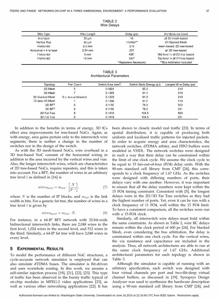
Similarly, all interswitch wire delays must hold withinthe same constraints. As shown in Table 2, wire RC delaysremain within the clock period of 600 ps [24]. For StackedMesh, even considering the bus arbitration, the delay isconstrained within one clock cycle. For the vertical wires,the via resistance and capacitance are included in theanalysis. Thus, all network architectures are able to run atthe same clock frequency of 1.67 GHz. Additionalarchitectural parameters for each topology is shown inTable 3.
Although the simulator is capable of running with anarbitrary specification, each switch was designed withfour virtual channels per port and two-flit-deep virtualchannel buffers, as discussed in [19]. Synopsys DesignAnalyzer was used to synthesize the hardware descriptionusing a 90-nm standard cell library from CMP [24], and
FEERO AND PANDE: NETWORKS-ON-CHIP IN A THREE-DIMENSIONAL ENVIRONMENT: A PERFORMANCE EVALUATION 37
TABLE 2Wire Delays
TABLE 3Architectural Parameters
Authorized licensed use limited to: Washington State University. Downloaded on June 16,2010 at 22:16:56 UTC from IEEE Xplore. Restrictions apply.

Synopsys PrimePower was used to gather energy dissipa-
tion statistics. To calculate Eswitch and Einterconnect from (4),
we follow the methodology discussed in [19]. We
determine the energy dissipated by each switch, Eswitch,
by running its gate-level netlist through Synopsys Prime-
Power using large sets of input data patterns. In order to
determine the interconnect energy, Einterconnect, we esti-
mate the interconnects’ capacitance, taking into account
each interswitch wire’s specific layout, by the following
expression [19]:
Cinterconnect ¼ Cwire � waþ1;a þ n �m � ðCG þ CJÞ; ð9Þ
where Cwire represents the capacitance per unit length of the
wire, waþ1;a is the wire length between two consecutive
switches, n is the number of repeaters, m represents the size
of those repeaters with respect to minimum size devices,
and last, CG and CJ represent the gate and junction
capacitances, respectively, of a minimum size inverter. We
consider a worst case scenario where adjacent wires switch
in opposite directions while determining Cwire [25].The simulation is initially run for 10,000 cycles to allow
the 64-IP network to stabilize, and it is subsequently run for
100,000 more cycles. The simulator provides statistics for
energy, throughput, and latency.
5.1 Mesh-Based Networks
We first consider the performance of 3D mesh-based NoCarchitectures. Fig. 6a shows the variation of throughput as afunction of the injection load. A network cannot acceptmore traffic than is supplied, and limitations in routing andcollisions cause saturation before throughput reaches unity.From Fig. 6a, we see clearly that both the 3D Mesh andStacked Mesh topologies exhibit throughput improvementsover their 2D counterparts. It is also clear that the ciliated3D Mesh network shows only a small throughput improve-ment. However, this is not where a ciliated structureexhibits the best performance. It will be shown later thatthis network topology has significant benefits both in termsof energy dissipation and silicon area.
These results coincide with the analysis of 3D mesh-based NoC provided in Section 4.1. We have shown in (1)that a 3D mesh will have 29 percent more interconnectionlinks than a 2D version; hop count calculations have shownthat a flit in a 2D mesh network will, on average, traverse40 percent more hops than a flit navigating a 3D mesh(according to Table 4); and 3D mesh switches have higherconnectivity with the increased number of ports. These allaccount for throughput improvements. In general, thelower hop count allows a wormhole-routed packet tooccupy fewer resources, freeing up links for additionalpackets. Consequently, there is a corresponding increase inthroughput.
38 IEEE TRANSACTIONS ON COMPUTERS, VOL. 58, NO. 1, JANUARY 2009
Fig. 6. Experimental results for mesh-based NoCs. (a) Throughput versus injection load. (b) Latency versus injection load. (c) Cycle energy versus
injection load. (d) Packet energy.
Authorized licensed use limited to: Washington State University. Downloaded on June 16,2010 at 22:16:56 UTC from IEEE Xplore. Restrictions apply.

Next, we consider the Stacked Mesh architecture. Anincrease in throughput is evident, as shown in Fig. 6a.However, with a 32-bit bus (corresponding to the flit width)connecting the layers of the NoC, throughput improve-ments are not as substantial as with the 3D mesh.Contention issues in the bus limit the attainable perfor-mance gains. Yet, since communication between layers isbus based, we can increase the size of the bus withoutmodifying the switch architectures. As a result, the buswidth is increased to 128 bits. Any further increase did nothave any significant impact on throughput, except toincrease the total capacitance on the bus. With thisimprovement, Stacked Mesh saturates at a slightly higherinjection load than a 3D Mesh network. The Stacked Meshtopology also offers a lower hop count in comparison to astrict 3D mesh. From (3), we see that the average hop countis equal to 3.42. With the lower hop count in addition to thewide, 128-bit bus for vertical transmission, this architectureoffers the highest throughput among all the 3D mesh-basednetworks.
Throughput characteristics of the ciliated 3D Meshtopology differ significantly from the other 3D networks.This network has a saturating throughput that is slightlyhigher than a 2D Mesh network and considerably less thanboth 3D Mesh and Stacked Mesh networks. This is truedespite having the lowest hop count at an average of3.10 hops. However, with only 64 interswitch links,compared to 144 in the 3D Mesh and 112 in the 2D Mesh,throughput improvements due to hop count are negated bythe reduced number of links. The fact that there aremultiple functional IP blocks for every switch is alsoresponsible for considerably lower throughput due tocontention issues in the switches.
Fig. 6b depicts the latencies for the architectures underconsideration. Here, it is seen that 3D mesh-based NoCshave superior latency characteristics over the 2D versions.This is a product of the reduced hop count characteristic of3D mesh-based topologies.
Energy dissipation characteristics for 3D mesh-basedNoCs reveal a substantial improvement over planar NoCs.The energy dissipation profiles of the mesh-based NoCarchitectures under consideration are shown in Fig. 6c.Energy dissipation is largely dependent on two factors:architecture and injection load. We consider these twoparameters as the independent factors in our analysis. Asshown in (4), the energy dissipation in an NoC depends onthe energy dissipated by the switch blocks and theinterswitch wire segments. Both these factors depend onthe architectures. The design of the switch varies with thearchitecture, and interswitch wire length is also architecturedependent [19]. Besides the network architecture, injectionload has a clear effect on the total energy dissipation of a
NoC, in accordance with Fig. 6c. Intuitively, it is clear thatwith more packets traversing the network, power willincrease. This is why packet energy, in Fig. 6d, is animportant attribute for characterizing NoC structures.Notice that, at saturation, a 2D Mesh network dissipatesless power than both Stacked Mesh and 3D Mesh networks.This is the result of the lower 2D Mesh throughput, and the3D networks consume more energy because they transmitmore flits at saturation. Packet energy is a more accuraterepresentation of the cost of data transmission. With packetenergy in mind, it can be seen that every 3D topologyprovides a very substantial improvement over 2D mesh.Also, the energy dissipation of the ciliated mesh topology isless, still, than that of the 3D mesh network. These resultsfollow closely the hop count calculations summarized inTable 4, with the exception of the packet energy for aStacked Mesh network. Energy is heavily dependant oninterconnect energy, and this is where the Stacked Meshsuffers. Since vertical communication takes place throughwide buses, the capacitive loading on those buses results ina significant amount of energy. As a result, though 3DStacked Mesh has a lower hop count compared to 3D Mesh,it dissipates more packet energy on average. Regardless, theprofound energy savings possible in these 3D architecturesprovides serious motivation for a SoC designer to consider a3D IC.
The final performance metric considered in this study isthe overall area overhead incurred with the instantiation ofthe various networks. Fig. 7 shows the area penalty fromeach NoC design, both in terms of switch area andinterconnect area. We see that while the 3D Mesh andStacked Mesh NoCs reduce the amount of wiring area,switch overhead is increased. For both 3D Mesh andStacked Mesh NoCs, the number of longer interswitch linksin x�y plane is reduced. There are 96 x�y links for bothtopologies, for Stacked Mesh, 16 buses are present, and forthe 3D Mesh, 48 vertical links are present. In comparison,the conventional 2D mesh-based NoC has 112 links in thehorizontal plane. As the 3D NoCs have fewer longhorizontal links, they incur less wiring area overhead.Although there are a large number of vertical links, theamount of area incurred by them is very small due to the2 �m� 2 �m interlayer vias. However, an increased numberof ports per switch results in larger switch overhead for
FEERO AND PANDE: NETWORKS-ON-CHIP IN A THREE-DIMENSIONAL ENVIRONMENT: A PERFORMANCE EVALUATION 39
Fig. 7. Area overhead for mesh-based NoCs.
TABLE 4Average Hop Count in Mesh-Based NoCs
Authorized licensed use limited to: Washington State University. Downloaded on June 16,2010 at 22:16:56 UTC from IEEE Xplore. Restrictions apply.

both of these NoC architectures, ultimately causing the 3DMesh and Stacked Mesh topologies to incur more siliconarea in spite of wiring improvements. On the other hand,ciliated 3D Mesh shows a significant improvement in termsof area. The 4 � 4 � 2 ciliated 3D Mesh structure involveshalf the number of switches as the other mesh-basedarchitectures in addition to only 64 links. As a result, thearea overhead is accordingly smaller.
5.2 Tree-Based Networks
In this section, we evaluate the performance of the 3D tree-based NoCs. It has already been established that 2D and3D versions of the tree topologies should have identicalthroughput and latency characteristics, and Figs. 8a and 8bsupport this. Consistent with the analysis of mesh-basedNoCs, Fig. 8a shows the variation of throughput as afunction of injection load, and Fig. 8b shows the effect ofinjection load on latency. The assumption here was thatthe switches and the interswitch wire segments are drivenby the same clock as explained earlier. Consequently,under this assumption, in terms of throughput and latencythere is no advantage to choosing a 3D IC over atraditional planar IC for a tree-based NoC. However, thisis eclipsed by the superior performance achieved in termsof energy and area overhead. If the NoC switches can bedesigned to operate as fast as the interswitch wires, thenwe will show in Section 5.4 that the 3D tree-based
architectures will have significant benefit in terms of evenlatency and bandwidth.
The energy profiles for 3D tree-based NoCs (Fig. 8c)reveal significant improvements over 2D implementations.Both BFT and fat tree (SPIN) networks show a very largereduction in energy when 3D ICs are used. Once again, wesee that energy dissipation is largely dependant both onarchitecture and injection load. Each NoC shows thatenergy dissipation increases with injection load until thenetwork becomes saturated, similar to the throughput curveshown in Fig. 8a. From the energy profiles, we also see thatthe fat tree networks cause higher energy dissipation thanthe BFT instantiations, but this is universally true only athigh injection load.
Again, this is the motivation to consider packet energy ofthe networks as a relevant metric for comparison, as shownin Fig. 8d. Energy savings in excess of 45 percent areachievable by adopting 3D ICs as a manufacturing metho-dology, and both BFT and fat tree networks show similarimprovements. In case of tree-based NoCs, where the basicnetwork topology remains unchanged in 3D implementa-tions, all improvements in energy dissipation are caused bythe shorter wires. As we showed earlier in Table 1, a3D structure greatly reduces the interswitch wire length.The overall energy dissipation in a NoC is heavilydependant on the interconnect energy, and this reductionin interswitch wire length effects very large savings.
40 IEEE TRANSACTIONS ON COMPUTERS, VOL. 58, NO. 1, JANUARY 2009
Fig. 8. Experimental results for tree-based NoCs. (a) Throughput versus injection load. (b) Latency versus injection load. (c) Cycle energy versus
injection load. (d) Packet energy.
Authorized licensed use limited to: Washington State University. Downloaded on June 16,2010 at 22:16:56 UTC from IEEE Xplore. Restrictions apply.

Besides advantages in terms of energy, 3D ICs enabletree-based NoCs to reduce silicon area overhead by asizable margin. Fig. 9 shows the overall area overhead oftree-based NoCs. We see that although no improvementsare made in terms of switch area, the reductions ininterswitch wire lengths and amount of repeaters areresponsible for substantial reductions in wiring overhead.This is especially true for the fat tree network, which hasmore interconnects in the higher levels of the tree; wiringoverhead is reduced more than 60 percent by instantiatingthe network into a 3D IC.
5.3 Effects of Traffic Localization
Until this point, we have assumed a uniform spatialdistribution of traffic. In a SoC environment, differentfunctions would map to different parts of the chip and thetraffic patterns would be expected to be localized todifferent degrees [26]. We therefore studied the effect oftraffic localization on the performance of the 3D NoCs andconsidered the illustrative case of spatial localization wherelocal messages travel from a source to the set of the nearestdestinations. In the case of BFT and fat tree, localized trafficis constrained to within a cluster consisting of a singlesubtree, while, in the case of 3D Mesh, it is constrained towithin the destinations placed at the shortest Manhattandistance [19].
On the other hand, the 3D Stacked Mesh architecture iscreated simply to take advantage of the inexpensive verticalcommunication. The research pursued by Li et al. [12]suggested that in a 3D multiprocessor SoC, much of thecommunication should take place vertically, taking advan-tage of the short interlayer wire segments. This is a result ofa large proportion of network traffic occurring between theprocessor and the closest cache memories, which are oftenplaced along the z-dimension. Consequently, in thesesituations, the traffic will be highly localized, and wetherefore consider localized traffic to be constrained towithin a pillar for Stacked Mesh. Fig. 10 summarizes these
FEERO AND PANDE: NETWORKS-ON-CHIP IN A THREE-DIMENSIONAL ENVIRONMENT: A PERFORMANCE EVALUATION 41
Fig. 9. Area overhead for tree-based NoCs.
Fig. 10. Localization effects on mesh-based NoCs in terms of (a) throughput and (b) packet energy and localization effects on tree-based NoCs interms of (c) throughput and (d) packet energy.
Authorized licensed use limited to: Washington State University. Downloaded on June 16,2010 at 22:16:56 UTC from IEEE Xplore. Restrictions apply.
effects, revealing the benefits of traffic localization. Morepackets can be injected into the network, improving thethroughput characteristics of each topology, as shown inFigs. 10a and 10c, which also shows the throughput profileof the 2D topologies for reference. Analytically, increasinglocalization reduces the average number of hops that a flitmust travel from source to destination.
Fig. 10a reveals that the stacked mesh network providesbest performance in terms of throughput in the presence oflocalized traffic. However, this is achieved by using a widebus for vertical communication. Let us consider what occurswhen the bus size is equal to the flit width of 32 bits. Withlow localization, the achieved throughput is higher thanthat in a 2D Mesh network. However, when the fraction oflocalized traffic in the vertical pillars is increased, a hugeperformance degradation is seen. This is due to thecontention in the bus. When the bus width is increased to128 bits, throughput increases significantly with increase inlocalized traffic. This happens due to less contention in awider communication channel.
Figs. 10b and 10d depict the effects of localization onpacket energy, and unsurprisingly, there is a highly linearrelationship between these two parameters. Packet energyis highly correlated with the number of hops from source todestination, and the resultant reduction of packet energywith localization supports this correlation. For the mesh-based networks, ciliated 3D Mesh exhibits the lowest packetenergy due to its low hop count and very short verticalwires. In fact, at highest localization, the packet energy for aciliated 3D Mesh topology is less than 50 percent of that ofthe next-best-performing topology: 3D Mesh. For the tree-based NoCs, both 3D networks have much-improvedpacket energy with traffic localization.
As can be seen from Fig. 10, there are trade-offs betweenpacket energy and throughput. For instance, the best-performing topology in terms of energy, ciliated 3D Mesh,operates at the lowest throughput even when traffic ishighly localized. On the other hand, although a 3D StackedMesh network with wider bus width achieves superiorthroughput without necessitating a highly local trafficdistribution, it incurs more energy dissipation than otherstructures under local traffic due to the capacitive loadingon the interlayer buses. However, the other topologies lie insome middle ground between these two extremes, and ingeneral, it is clear that 3D ICs continue to effect improve-ments on NoCs under localized traffic.
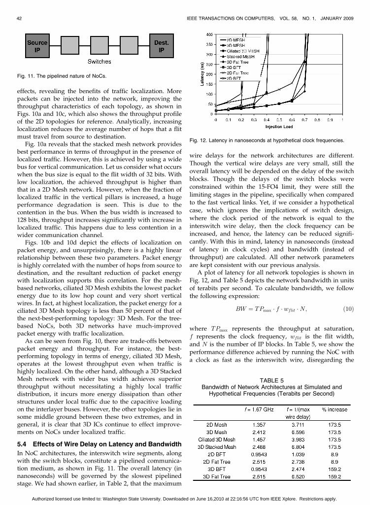
5.4 Effects of Wire Delay on Latency and Bandwidth
In NoC architectures, the interswitch wire segments, alongwith the switch blocks, constitute a pipelined communica-tion medium, as shown in Fig. 11. The overall latency (innanoseconds) will be governed by the slowest pipelinedstage. We had shown earlier, in Table 2, that the maximum
wire delays for the network architectures are different.Though the vertical wire delays are very small, still the
overall latency will be depended on the delay of the switch
blocks. Though the delays of the switch blocks wereconstrained within the 15-FO4 limit, they were still the
limiting stages in the pipeline, specifically when compared
to the fast vertical links. Yet, if we consider a hypotheticalcase, which ignores the implications of switch design,
where the clock period of the network is equal to the
interswitch wire delay, then the clock frequency can beincreased, and hence, the latency can be reduced signifi-
cantly. With this in mind, latency in nanoseconds (instead
of latency in clock cycles) and bandwidth (instead ofthroughput) are calculated. All other network parameters
are kept consistent with our previous analysis.A plot of latency for all network topologies is shown in
Fig. 12, and Table 5 depicts the network bandwidth in units
of terabits per second. To calculate bandwidth, we followthe following expression:
BW ¼ TPmax � f � wflit �N; ð10Þ
where TPmax represents the throughput at saturation,
f represents the clock frequency, wflit is the flit width,and N is the number of IP blocks. In Table 5, we show the
performance difference achieved by running the NoC with
a clock as fast as the interswitch wire, disregarding the
42 IEEE TRANSACTIONS ON COMPUTERS, VOL. 58, NO. 1, JANUARY 2009
Fig. 11. The pipelined nature of NoCs.
Fig. 12. Latency in nanoseconds at hypothetical clock frequencies.
TABLE 5Bandwidth of Network Architectures at Simulated and
Hypothetical Frequencies (Terabits per Second)
Authorized licensed use limited to: Washington State University. Downloaded on June 16,2010 at 22:16:56 UTC from IEEE Xplore. Restrictions apply.

switch design constraints. It is evident that the tree-basedarchitectures show the greatest performance improvementin this scenario going from 2D to 3D implementations, asthe horizontal wire lengths are also reduced.
5.5 Network Aspect Ratio
The ability to stack layers of silicon is not withoutnuances. Upcoming 3D processes have a finite numberof layers due to manufacturing difficulties and yield issues[7]. Furthermore, it is speculated [7] that the number oflayers in a chip stack is not likely to scale with transistorgeometries. This has a nontrivial effect on the performanceof 3D NoCs. Consequently, future NoCs may have agreater number of IP blocks in the horizontal dimensionsthan vertically. The effect of this changing aspect ratiomust be characterized.
For an illustration of these effects, we will examine,more in depth, the performance of a mesh-based NoC in atwo-layer IC in comparison to the previously analyzed 3D4 � 4 � 4 Mesh and 2D 8 � 8 Mesh. Here, we consider a64-IP 8 � 4 � 2 Mesh to match the 64-IP network size, inorder to make the comparison of latency and energy as fairas possible, and a 60-IP 6 � 5 � 2 Mesh to show anetwork that is similar in size and that results in amore square overall footprint than the 8 � 4 � 2 Mesh.Fig. 13 summarizes our analysis of these two-layer ICs.Throughput characteristics are seen in Fig. 13a. We
see clearly that the 6 � 5 � 2 Mesh achieves asignificantly higher throughput than the 2D 8 � 8 Meshand the 8 � 4 � 2 Mesh, which suffers from a high averagehop count (4.44 versus 4.11 for the 6 � 5 � 2 Mesh), whileachieving a lower maximum throughput than the four-layer mesh. Likewise, the two-layer mesh NoCs outper-form the 2D Mesh in terms of latency, as shown in Fig. 13b,without exceeding the performance of the four-layer 3Dinstantiation. This trend continues when considering cycleenergy (Fig. 13c) and packet energy (Fig. 13d). Theseresults are as expected. With the first layer added, we seesignificant improvements in terms of each performancemetric over the 2D case. Though the multilayer NoCexhibits superior performance characteristics compared toa 2D implementation, it will have to circumvent significantmanufacturing challenges. Yet, even if we are limited to atwo-layer 3D realization, that will still significantly out-perform the planar NoCs.
5.6 Multilayer IPs
Throughout this paper, we have assumed each IP block tobe instantiated in one layer of silicon. However, asdiscussed in [14], it is certainly possible for the IP blocksto be designed using multiple layers. So, each networkarchitecture is analyzed with multilayer IPs. We assume thepipelined communication shown in Fig. 11, i.e., the NoCsare constrained by the switch delay and it cannot be driven
FEERO AND PANDE: NETWORKS-ON-CHIP IN A THREE-DIMENSIONAL ENVIRONMENT: A PERFORMANCE EVALUATION 43
Fig. 13. Comparing two 2-layer NoCs. (a) Throughput versus injection load. (b) Latency versus injection load. (c) Cycle energy versus injection load.
(d) Packet energy.
Authorized licensed use limited to: Washington State University. Downloaded on June 16,2010 at 22:16:56 UTC from IEEE Xplore. Restrictions apply.

as fast as the interswitch wire. Considering this, multilayerIPs have no effect on either throughput or latency(assuming the same clock frequency for all networks), butthere are nontrivial effects on the energy dissipation profile.This effect on packet energy is depicted in Fig. 14. Theenergy savings come from reduced horizontal wire lengths.For instance, if a 2.5 mm� 2.5 mm IP block is instantiated intwo layers, the IP’s circuitry is spread over two layers, andthe footprint reduces by a factor of 1.414. Similarly, ifinstantiated in three layers, the footprint reduces by a factorof 1.732, and with four layers, the factor is 2. Although thevertical wire lengths are increased two, three, and fourtimes, respectively, in order to span the entire multilayer IP,the negative effects on energy incurred by this are eclipsedby the significant reductions in horizontal wire lengths.However, multilayer IPs increase the number of layers in a3D IC, placing an increased burden on manufacturability.
6 CONCLUSION
Three-dimensional NoCs are natural extensions of 2Ddesigns. In this paper, we have demonstrated that besidesreducing the footprint in a fabricated design, 3D networkstructures provide a better performance compared totraditional, 2D NoC architectures. We have demonstratedthat both mesh and tree-based NoCs are capable ofachieving better performance when instantiated in a 3DIC environment compared to more traditional 2D imple-mentations. The mesh-based architectures show significantperformance gains in terms of throughput, latency, andenergy dissipation with a small area overhead. On the otherhand, the 3D tree-based NoCs achieve significant gain inenergy dissipation and area overhead without any changein throughput and latency. However, if the NoC switchesare designed to be as fast as the interconnect, even the 3Dtree-based NoCs will exhibit performance benefits in termsof latency and bandwidth. The NoC paradigm continues toattract significant research attention in both academia andindustry. With the advent of 3D ICs, the achievableperformance benefits from NoC methodology will be morepronounced as shown in this paper. Consequently, this willfacilitate adoption of the NoC model as a mainstreamdesign solution for larger multicore system chips.
REFERENCES
[1] L. Benini and G. De Micheli, “Networks on Chips: A New SoCParadigm,” Computer, pp. 70-78, Jan. 2002.
[2] P. Magarshack and P.G. Paulin, “System-on-Chip beyond theNanometer Wall,” Proc. 40th Design Automation Conf. (DAC ’03),pp. 419-424, 2003.
[3] W.J. Dally and B. Towles, “Route Packets, Not Wires: On-ChipInterconnection Networks,” Proc. 38th Design Automation Conf.(DAC ’01), pp. 683-689, June 2001.
[4] M.A. Horowitz et al., “The Future of Wires,” Proc. IEEE, vol. 89,no. 4, pp. 490-504, Apr. 2001.
[5] C. Grecu, P.P. Pande, A. Ivanov, and R. Saleh, “Timing Analysis ofNetwork on Chip Architectures for MP-SoC Platforms,” Micro-electronics J., vol. 36, no. 9, pp. 833-845, Sept. 2005.
[6] H.G. Lee et al., “On-Chip Communication Architecture Explora-tion: A Quantitative Evaluation of Point-to-Point, Bus, andNetwork-on-Chip Approaches,” ACM Trans. Design Automationof Electronic Systems, vol. 12, no. 3, pp. 1-20, Aug. 2007.
[7] A.W. Topol et al., “Three-Dimensional Integrated Circuits,” IBM J.Research and Development, vol. 50, nos. 4/5, July-Sept. 2006.
[8] W.R. Davis et al., “Demystifying 3D ICS: The Pros and Cons ofGoing Vertical,” IEEE Design and Test of Computers, vol. 22, no. 6,Nov./Dec. 2005.
[9] Y. Deng et al., “2.5D System Integration: A Design Driven SystemImplementation Schema,” Proc. Asia and South Pacific DesignAutomation Conf. (ASP-DAC), 2004.
[10] M. Ieong et al., “Three Dimensional CMOS Devices and IntegratedCircuits,” Proc. IEEE Custom Integrated Circuits Conf. (CICC), 2003.
[11] P. Jacob et al., “Predicting the Performance of a 3D Processor-Memory Stack,” IEEE Design and Test of Computers, vol. 22, no. 6,pp. 540-547, Nov./Dec. 2005.
[12] F. Li et al., “Design and Management of 3D Chip MultiprocessorsUsing Network-in-Memory,” Proc. 33rd Int’l Symp. ComputerArchitecture (ISCA ’06), pp. 130-141, June 2005.
[13] C. Addo-Quaye, “Thermal-Aware Mapping and Placement for 3DNoC Designs,” Proc. IEEE Int’l System on Chip Conf. (SOCC ’05),pp. 25-28, 2005.
[14] V.F. Pavlidis and E.G. Friedman, “3-D Topologies for Networks-on-Chip,” IEEE Trans. Very Large Scale Integration (VLSI ’07),pp. 1081-1090, Oct. 2007.
[15] S. Vangal et al., “An 80-Tile 1.28TFLOPS Network-on-Chip in65 nm CMOS,” Proc. IEEE Int’l Solid-State Circuits Conf. (ISSCC ’07),pp. 98-99, 2007.
[16] R.I. Greenberg and L. Guan, “An Improved Analytical Model forWormhole Routed Networks with Application to Butterfly FatTrees,” Proc. Int’l Conf. Parallel Processing (ICPP ’97), pp. 44-48,Aug. 1997.
[17] C. Grecu et al., “A Scalable Communication-Centric SoC Inter-connect Architecture,” Proc. Fifth Int’l Symp. Quality ElectronicDesign (ISQED ’04), pp. 343-348, 2004.
[18] P. Guerrier and A. Greiner, “A Generic Architecture for On-ChipPacket-Switched Interconnections,” Proc. Design, Automation andTest in Europe (DATE ’00), pp. 250-256, Mar. 2000.
[19] P.P. Pande, C. Grecu, M. Jones, A. Ivanov, and R. Saleh,“Performance Evaluation and Design Trade-Offs for Network onChip Interconnect Architectures,” IEEE Trans. Computers, vol. 54,no. 8, pp. 1025-1040, Aug. 2005.
[20] J. Duato, S. Yalamanchili, and L. Ni, Interconnection Networks—AnEngineering Approach. Morgan Kaufmann, 2002.
[21] K. Park and W. Willinger, Self-Similar Network Traffic andPerformance Evaluation. John Wiley and Sons, 2000.
[22] D.R. Avresky, V. Shubranov, R. Horst, and P. Mehra, “Perfor-mance Evaluation of the ServerNetR SAN under Self-SimilarTraffic,” Proc. 13th Int’l and 10th Symp. Parallel and DistributedProcessing (IPPS/SPDP ’99), pp. 143-147, Apr. 1999.
[23] G.V. Varatkar and R. Marculescu, “On-Chip Traffic Modelingand Synthesis for MPEG-2 Video Applications,” IEEE Trans. VeryLarge Scale Integration (VLSI) Systems, vol. 8, no. 3, pp. 335-339,June 2000.
[24] Circuits Multi-Projects, http://cmp.imag.fr/, 2008.[25] K.C. Saraswat et al., “Technology and Reliability Constrained
Future Copper Interconnects—Part II: Performance Implications,”IEEE Trans. Electron Devices, vol. 49, no. 4, pp. 598-604, Apr. 2002.
[26] P.P. Pande, C. Grecu, M. Jones, A. Ivanov, and R. Saleh, “Effect ofTraffic Localization on Energy Dissipation in NoC-Based Inter-connect,” Proc. IEEE Int’l Symp. Circuits and Systems (ISCAS ’05),pp. 1774-1777, May 2005.
44 IEEE TRANSACTIONS ON COMPUTERS, VOL. 58, NO. 1, JANUARY 2009
Fig. 14. The effect of multilayer IPs.
Authorized licensed use limited to: Washington State University. Downloaded on June 16,2010 at 22:16:56 UTC from IEEE Xplore. Restrictions apply.

Brett Stanley Feero received the BS degreein computer engineering (summa cum laude)and the MS degree in computer engineeringfrom Washington State University, Pullman, in2006 and 2008, respectively. His researchinterests include system-on-chip communica-tion, networks-on-chip, and 3D integratedcircuits. After his graduation, he became anengineer in Fabric IP at ARM, Cambridge,United Kingdom. He is a member of Tau Beta
Pi and a member of the IEEE.
Partha Pratim Pande received the MS degreein computer science from the National Uni-versity of Singapore in 2002 and the PhDdegree in electrical and computer engineeringfrom the University of British Columbia in 2005.He is an assistant professor in the School ofElectrical Engineering and Computer Science,Washington State University, Pullman. Hisprimary research interests lie in the areas ofdesign and test of networks-on-chip, fault
tolerance and reliability of multiprocessor SoC (MP-SoC) platforms,3D integration, and on-chip wireless communication network. Heserves in the program committees of various international confer-ences, including the IEEE International On-Line Testing Symposium(IOLTS), Asian Test Symposium (ATS), IEEE International MidwestSymposium on Circuits and Systems (MWSCAS), and IEEE Interna-tional Symposium on Electronic Design, Test and Applications(DELTA). He is a member of the IEEE.
. For more information on this or any other computing topic,please visit our Digital Library at www.computer.org/publications/dlib.
FEERO AND PANDE: NETWORKS-ON-CHIP IN A THREE-DIMENSIONAL ENVIRONMENT: A PERFORMANCE EVALUATION 45
Authorized licensed use limited to: Washington State University. Downloaded on June 16,2010 at 22:16:56 UTC from IEEE Xplore. Restrictions apply.