Embed Size (px)
Citation preview

2Lecture 1
Lecture 1
Design and Technology Trends
Overview
3Lecture 1
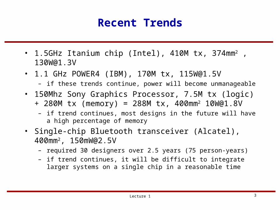
Recent Trends
• 1.5GHz Itanium chip (Intel), 410M tx, 374mm2 , [email protected]• 1.1 GHz POWER4 (IBM), 170M tx, [email protected]
– if these trends continue, power will become unmanageable
• 150Mhz Sony Graphics Processor, 7.5M tx (logic) + 280M tx (memory) = 288M tx, 400mm2 [email protected]
– if trend continues, most designs in the future will have a high percentage of memory
• Single-chip Bluetooth transceiver (Alcatel), 400mm2, [email protected]
– required 30 designers over 2.5 years (75 person-years)– if trend continues, it will be difficult to integrate larger systems on a single
chip in a reasonable time
4Lecture 1
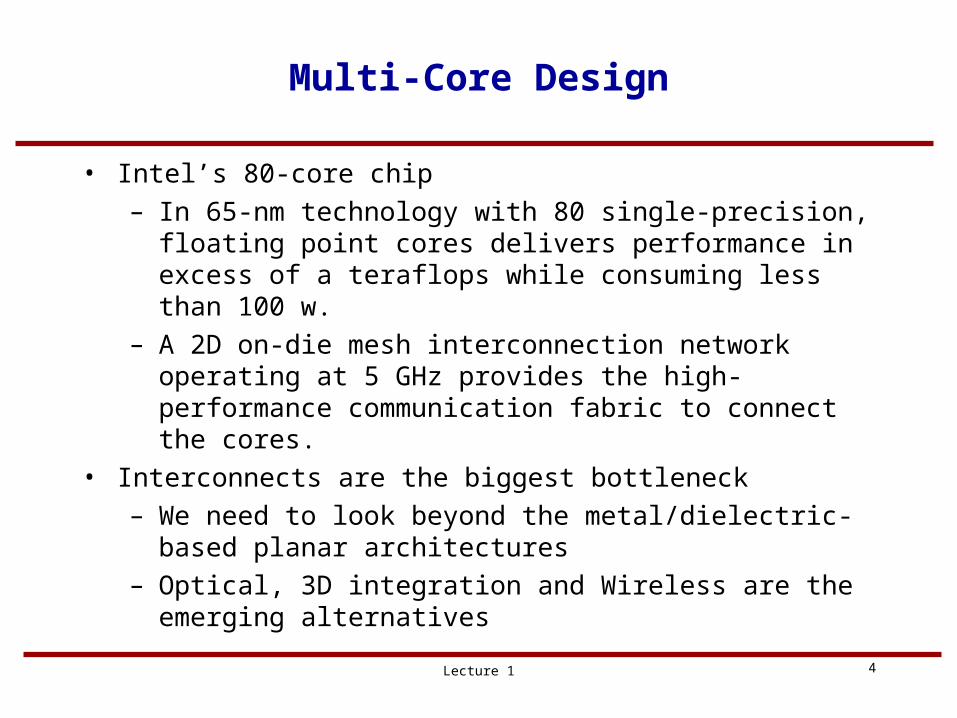
Multi-Core Design
• Intel’s 80-core chip– In 65-nm technology with 80 single-precision, floating point
cores delivers performance in excess of a teraflops while consuming less than 100 w.
– A 2D on-die mesh interconnection network operating at 5 GHz provides the high-performance communication fabric to connect the cores.
• Interconnects are the biggest bottleneck– We need to look beyond the metal/dielectric-based planar
architectures– Optical, 3D integration and Wireless are the emerging
alternatives

5Lecture 1
Multi-core applications
Nokia Sparrow
Intel LARRABEE

6Lecture 1
Three-Dimensional Integrated Circuits
• Coming in a big way• Multiple Layers of Active Devices• Driven by
– Limited floorplanning choices– Desire to integrate disparate technologies (GaAs, SOI, SiGe,
BiCMOS)– Desire to integrate disparate signals (analog, digital, RF)– Interconnect bottleneck
6
2D IC 3D IC
As small as 20µm

7Lecture 1
Photonic Communication
• High bandwidth photonic links for high payload transfers• Limitations on switch architecture
• More than 4-port designs are complex
• On-chip integration of photonic components

8Lecture 1
On-Chip RF/Wireless Interconnects
• Replace long distance wires• Use of waveguides out of
package or IC structures like parallel metal wires
• Chang et al. demonstrated Transmission Line based RF interconnect for on chip communication
– Not really wireless

9Lecture 1
Lower Latency and Energy Dissipation
Three Dimensional Integration
Optical Interconnects Wireless/RF Interconnects
Novel interconnect paradigms for Multicore designs

10Lecture 1
MOS Transistor Scaling(1974 to present)
Scaling factor s=0.7 per node (0.5x per 2 nodes)
Metal pitch Technology Nodeset by 1/2 pitch(interconnect)
Gate length(transistor)
Poly width

11Lecture 1
Ideal Technology Scaling (constant field)
Quantity Before Scaling After Scaling
Channel Length L L’ = L * s
Channel Width W W’ = W * s
Gate Oxide thickness tox t’ox = tox * s
Junction depth xj x’j = xj * s
Power Supply Vdd Vdd’ = Vdd * s
Threshold Voltage Vth V’th = Vth * s
Doping Density, p n+
NA ND
NA’ = NA / s ND’ = ND / s

12Lecture 1
Technology Nodes 1999-2019
180nm 130nm 90nm 65nm 45nm 32nm 22nm 16nm
1999 2001 2004 2007 2010 2013 2016 2019
0.7x 0.7x
0.5x
N-1 N N+1
Two year cycle between nodes until 2001, then 3 year cycle begins.

13Lecture 1
10
100
1000
Dec-83 Dec-86 Dec-89 Dec-92 Dec-95 Dec-98
8038680486PentiumPentium II
Expon.
MPU Clock Frequency Trend
Intel: Borkar/Parkhurst

14Lecture 1
10
100
1000
Dec-83 Dec-86 Dec-89 Dec-92 Dec-95 Dec-98
8038680486PentiumPentium II
Expon.
MPU Clock Frequency Trend
Intel: Borkar/Parkhurst
Dec-99 Dec-00 Dec-01 Dec-02
10000Forward projectionmay be too optimistic
P4

15Lecture 1
10.00
100.00
Dec-83 Dec-86 Dec-89 Dec-92 Dec-95 Dec-98
8038680486PentiumPentium II
Expon.
MPU Clock Cycle Trend (FO4 Delays)
Intel: Borkar/Parkhurst

16Lecture 1
Delay vs Fanout
0
1
2
3
4
5
6
0 2 4 6 8
Fanout
De
lay
γ=0.0
γ=0.5
γ=1.0
γ=2.0
where is ratio of
Parasitic output
Capacitance to gate
capacitance
CIN Cload
1X 4X 16X
Optimal Sizing - FO4 Concept
Use FO4 delay as optimal delay

17Lecture 1
Clock cycle trend
FO4delay
D Q
C lk
D Q
C lk
L ogic
N
1000ps = 25 FO4
40ps
(a) (b)
Clock
Data

18Lecture 1
MPU Trends - Moore’s Law
4004400480088008
8080808080858085 80868086
286286386386
486486PentiumPentium®® proc proc
P6P6
0.0010.001
0.010.01
0.10.1
11
1010
101000
1,0001,000
10,00010,000
’’7070 ’’8080 ’’9090 ’’0000 ’’1010
TransistorsTransistors(MT)(MT)
2X Growth2X Growthin 2 Years!in 2 Years!
Transistors DoubleTransistors DoubleEvery Two YearsEvery Two Years
Source: Intel

19Lecture 1
More MPU Trends
PentiumPentium®® Pro proc Pro proc
PentiumPentium®® proc proc486486386386
28628680868086
80858085
80808080
80088008
40044004
41413636
32322828
11
1010
100100
’’7070 ’’8080 ’’9090 ’’0000 ’’1010
Die sizeDie size(mm)(mm)
~7% growth per year~7% growth per year
~2X growth in 10 years~2X growth in 10 years
~40mm Die in 2010?~40mm Die in 2010?
Source: Intel

20Lecture 1
What about power in the future?
0.10.1
11
1010
100100
1,0001,000
10,00010,000
’’7171 ’’7474 ’’7878 ’’8585 ’’9292 ’’0000 ’’0404 ’’0808
PowerPower(Watts)(Watts)
40044004
8008800880808080
80858085
80868086
286286
386386
486486
PentiumPentium®®
processorsprocessors
Power Projections Too High!Power Projections Too High!
Hot PlateHot PlateNuclear ReactorNuclear Reactor
Rocket NozzleRocket NozzleSun’s SurfaceSun’s Surface
Source: Intel

21Lecture 1
Problem with Power and Speed
• Power knob running out– Speed == Power– 10W/cm2 limit for convection cooling, 50W/cm2 limit for forced-air cooling– Large currents, large power surges on wakeup– Die size will not continue to increase unless more memory is used to occupy
the additional area– additional power dissipation coming from subthreshold leakage
• Speed knob running out– Historically, 2x clock frequency every process generation
• 1.4x from device scaling • 1.4x from pipelining, hence fewer logic stages (from 40-100 down to around 16 FO4
INV delays)– Clocks cannot be generated with period < 6-8 FO4 INV delays– Around 14-16 FO4 INV delays is limit for clock period
Unrealistic to continue 2x frequency trend!

22Lecture 1
Low-Power Application: PDA
0.18um / 400MHz / 470mW (typical)
CPU
I-cache32KB
D-cache32KB
I2C
FICP
USB
MMC
UART AC97
I2S
OST
GPIO
SSP
PWM RTC
DMA controller
LCDCnt.
MEMCnt.
PWR CPG
SDRAM64MB
Flash32MB
LCDPeripheral Area4 – 48MHz
Data Transfer Area
100MHz
Processor Area
Max 400MHz
MM Application MP3 JPEG Simple Moving Picture
6.5MTrs.
Available Time 6-10Hr
USB
MMC
KEY
Sound

23Lecture 1
Trends in Low-Power Design Content
• Today, SoC designs contain embedded processing engines such as CPU and DSP, and memory blocks such as SRAM and embedded DRAM
• As we scale technology and keep power constant how does the amount of logic vs. memory change?
• Consider the following assumptions to develop trends for on-chip logic/memory percentages
• Die size is 100mm2
• Clock frequency starts at 150MHz increases by about 40% per technology node
• Average power dissipation in limited to 100mW at 100oC• Initial condition at Year 2001: area percentage 75% logic, 25%
memory

24Lecture 1
ASIC Core Composition Breakout
0
10
20
30
40
50
60
1999 2000 2001
Per
cen
tgae
of
Die
Are
a (I
/Os
Exc
lud
ed)
Random Logic
Memory
Analog
Cores
ASIC Logic/Memory Content Trends
• Source: Dataquest (2001)
25Lecture 1
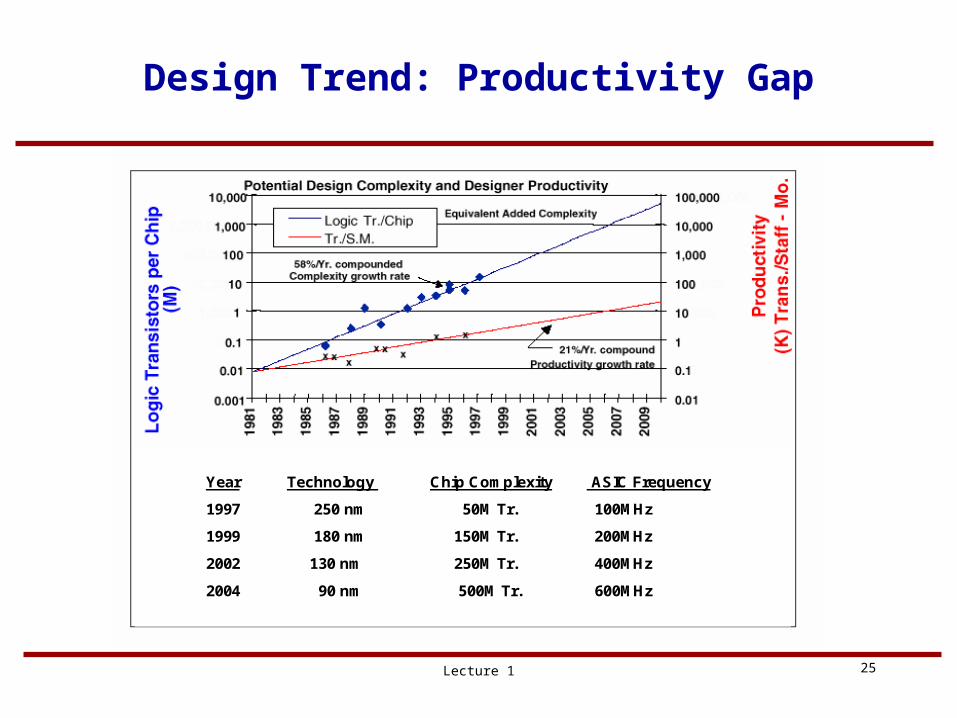
Design Trend: Productivity Gap
Year Technology Chip Complexity ASIC Frequency
1997 250 nm 50M Tr. 100MHz
1999 180 nm 150M Tr. 200MHz
2002 130 nm 250M Tr. 400MHz
2004 90 nm 500M Tr. 600MHz

26Lecture 1
Designing a 50M Transistor IC
• Gates Required ~12.5M
• Gates/Day (Verified) 1K (including memory)
• Total Eng. Days 12,500
• Total Eng. Years 35
• Cost/Eng./Year $200K
• Total People Cost $7M
• Other costs (masks, tools, etc.) $8M
Actual Cost is $10-15M to get actual prototypes after fabrication.

27Lecture 1
Productivity Gap
• Deep submicron (DSM) technology allows hundreds of millions of
transistors to be integrated on a single chip
• Number of transistors that a designer can design per day (~1000
gates/day) is not going up significantly
• New design methodologies are needed to address the
integration/productivity issues
“System on a chip” Design with reusable IP (Intellectual Property)
– new design methodology, IP development
– new HW/SW design and verification issues
– new test issues

28Lecture 1
SoC Design Hierarchy
SOC consists of new logic blocks and existing IP
New Logic blocks
Existing IP including memory
Each logic block can be implemented by newly designed portion and a re-use portion based on IPs
Newly designed portion
Re-use portion including memory

29Lecture 1
SoC Platform Design Concept
SoC Verification FlowSystem-Level PerformanceEvaluationRapid Prototype forEnd-Customer EvaluationSoC Derivative DesignMethodologies
System-level performanceevaluation environmentHW/SW Co-synthesisSoC IC Design Flows
ApplicationSpace
Methodology / Flows:
Foundation Block
MEM
FPGACPU Processor(s), RTOS(es)
and SW architecture
*IP can be hardware (digital or analog) or software. IP can be hard, soft or‘firm’ (HW), source orobject (SW)
*IP can be hardware (digital or analog) or software. IP can be hard, soft or‘firm’ (HW), source orobject (SW)
Scaleablebus, test, power, IO,clock, timing architectures
+ Reference Design
Foundry-SpecificPre-Qualification
Programmable IP
SW IP
Hardware IP
Pre-Qualified/VerifiedFoundation-IP*

30Lecture 1
Purpose of this Course
• This course addresses SoC design & test in DSM technologies• The goal is to present an overview of the various issues from
“Systems to Silicon” to provide a perspective on what is happening in technology and design.
• It is a very broad subject, one that industry is grappling with on a daily basis – one course cannot address all the issue properly
• We will begin with the Systems Level and work our way down to the Circuits Level
• The projects, presentations, and assignments will provide in-depth analysis of the subjects that are of interest to you

31Lecture 1
Syllabus
– Three broad categories– System on chip design and design for testability – Role of interconnects in contemporary SoC Design – Importance of Power and Low power SoC design
methodology
32Lecture 1
References
• Analysis and Design of Digital Integrated Circuits - In Deep Submicron Technology, Hodges, Jackson and Saleh, McGraw-Hill, Third Edition, 2004
• Essentials of Electronic Testing for Digital, Memory and Mixed-Signal VLSI Circuits by M. L. Bushnell and V. D. Agrawal, Boston: Springer, 2005, ISBN 0-7923-7991-8
• Journal Papers, Conference Papers, Course Notes.

33Lecture 1
Assignments
• There will be several homework and reading assignments. In reading assignments students are expected to read research papers and submit summaries. The reading list will be available on the course website. In class, you will be told which papers you should review.
• Each student will have the opportunity to present one paper to the class. The list of papers will be available in the course website. Each student should choose one of the listed papers.

34Lecture 1
Project
• One Design Project• List of possible projects will be provided• You are free to choose your own project. In that case
Instructor’s approval is needed.