Embed Size (px)
Citation preview

INTERNATIONAL JOURNAL OF RESEARCH IN COMPUTER APPLICATIONS AND ROBOTICS www.ijrcar.com
Vol.3 Issue.4, Pg.: 51-66
April 2015
G . S r e e R e d d y & K . V . K o t e s w a r a R a o
Page 51
INTERNATIONAL JOURNAL OF
RESEARCH IN COMPUTER
APPLICATIONS AND ROBOTICS
ISSN 2320-7345
32 – BIT ARITHMETIC AND LOGIC UNIT
DESIGN WITH OPTIMIZED AREA AND
LESS POWER CONSUMPTION BY USING
GDI TECHNIQUE
G. Sree Reddy1, K. V. Koteswara Rao
2
1PG Student, VLSI, Sree Vidyanikethan Engineering College, Tirupati, Chittoor, A.P, India.
2Assistant Professor, ECE Dept., Sree Vidyanikethan Engineering College, Tirupati, Chittoor, A.P, India.
Abstract: - The paper presents to design of 32-bit Arithmetic and Logic Unit by taking the advantage of
concept called Gate Diffusion Input Technique (GDI). Arithmetic and Logic Unit is the important block to
design the embedded and microprocessors. The Arithmetic Unit will do the arithmetic operations, as
ADDITION and SUBSTRACTION. The Logic unit will do the logic operations, as AND, OR, XOR and XNOR
by using the concept GDI technique. The simulation results were taken using the Digital Schematic tool in 120nm technology. The optimized Area and Power is calculated by using Micro Wind tool in 120 nm
technology. The simulation results tells that the design is more efficient compared with the CMOS logic, Pass
transistor logic and transmission gate logic with less area and power consumption.
Keywords: GDI technique, ALU, CMOS, Pass Transistor Logic.
1. Introduction
In VLSI field the integrated circuit technology is developing day to day life. However in recent years the circuits
designed with less area, power and propagation delay with low cost. The Arithmetic Logic Unit are designed
with less area and less power consumption and less propagation delay by reducing the number of transistors
count by using the concept called GDI technique. The Arithmetic and Logic Unit are used in high speed low
power application design processors. GDI technique reduces the Power supplies and Ground connections and
uses as inputs to the transistors.
Section II explains about the previous works. Section III explains Gate Diffusion Input technique.
Section IV contains Arithmetic and Logic unit operation. Section V analyses about the simulation results and
Section VI gives you the conclusion.
2. Previous Work
One bit full adder is main building block to design the 4-bit ALU. To design one bit full adder there are different
design techniques involved. Conventional CMOS, CPL, TFA, TG CMOS, C2MOS, Hybrid, Bridge, FA24T, N-
cell, DPL and Mod2f are the twelve states of arts to design the full adder. The above design techniques requires
the more number of transistors so that the area required to design will be more and takes high power
consumption. The combination of NMOS transistor and a PMOS transistor forms a CMOS transistor. The
number of transistors required to design CMOS full adder are 28 (no‟s). The figure 1 shows Schematic diagram

INTERNATIONAL JOURNAL OF RESEARCH IN COMPUTER APPLICATIONS AND ROBOTICS www.ijrcar.com
Vol.3 Issue.4, Pg.: 51-66
April 2015
G . S r e e R e d d y & K . V . K o t e s w a r a R a o
Page 52
of CMOS adder which consists of 28 transistors. The number of transistors required to design full adder by
using Transmission Gates technique is 14 numbers of transistors. The figure 2 shows a transmission gate full
adder which is generated by using 14 transistors. The power analysis and the number of transistors used in Pass
transistor logic, CMOS gates logic and ALU design by using GDI technique shown in the Table 3, table 4,
Table 5 and Table 6.
Figure 1 CMOS Full Adder Design
Figure 2 Full Adder Designed By using Transmission Gates
3. Gate Diffusion Input Technique
Gate Diffusion Input Technique is a new technique to reduce propagation delay, area and power dissipation. The
best method to design low power digital combinational circuits is GDI Technique. GDI technique is basically
two transistor implementation of complex logic functions which provides in-cell swing restoration under certain
operating conditions. The main feature of GDI cell is the VDD source will not connect to the source of PMOS
transistor and the GND will not connect to the source of NMOS transistor. In the place of VDD and GND pins
input signals are used to make more flexible than CMOS design. Figure 3 shows the Basic GDI cell. The figure
explains that there are three inputs in a Basic GDI cell. G(common gate input to NMOS and PMOS), p(input to the source/drain of PMOS) and N(input to the source/drain of NMOS). Table 1 shows the different logic
functions implemented with less power consumption and less propagation delay compared to other design
techniques.
Figure 3 Basic GDI cell

INTERNATIONAL JOURNAL OF RESEARCH IN COMPUTER APPLICATIONS AND ROBOTICS www.ijrcar.com
Vol.3 Issue.4, Pg.: 51-66
April 2015
G . S r e e R e d d y & K . V . K o t e s w a r a R a o
Page 53
Table 1 Logic functions of Basic GDI cell
The circuits required to design Arithmetic and Logic unit are
A. Multiplexer
B. XOR Gate
C. Full Adder
Multiplexer will acts as a digital switch. Selection line plays a major role to select particular input. If
the number of input lines is „2n‟ and selection lines will be „n‟ selection lines. With the „n‟ selection line the
particular „2n‟ input line will be selected. Figure 4 shows the implementation of 2x1 multiplexer and Figure 5 shows the layout of 2x1 multiplexer. The number of selection lines for 2x1 multiplexer is one selection line.
With respect to the select line the inputs will be selected. In the same way 4x1 multiplexer also designed to
execute arithmetic and logic unit. The number of selection lines required for 4x1 multiplexer is two and with
respect to the two selection lines the four inputs will be activated. Figure 6 shows the schematic of 4x1
multiplexer and figure 7 shows the layout of 4x1 multiplexer.
Figure 4 Schematic of GDI based 2x1 Multiplexer
Figure 5 Layout design of GDI based 2x1 Multiplexer

INTERNATIONAL JOURNAL OF RESEARCH IN COMPUTER APPLICATIONS AND ROBOTICS www.ijrcar.com
Vol.3 Issue.4, Pg.: 51-66
April 2015
G . S r e e R e d d y & K . V . K o t e s w a r a R a o
Page 54
Figure 6 Schematic of GDI based 4x1 Multiplexer
Figure 7 Layout design of GDI based 4x1 Multiplexer
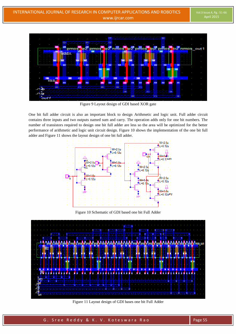
XOR gate is the main building block of the full adder and also which gives the sum output of the full adder. The
number of transistors taken to design the XOR gate is four. So the adder circuit can be improved by reducing the
area of XOR gate. Figure 8 shows the implementation of XOR gate and Figure 9 shows the layout design of the XOR gate.
Figure 8 Schematic of GDI based XOR gate
INTERNATIONAL JOURNAL OF RESEARCH IN COMPUTER APPLICATIONS AND ROBOTICS www.ijrcar.com
Vol.3 Issue.4, Pg.: 51-66
April 2015
G . S r e e R e d d y & K . V . K o t e s w a r a R a o
Page 55
Figure 9 Layout design of GDI based XOR gate
One bit full adder circuit is also an important block to design Arithmetic and logic unit. Full adder circuit
contains three inputs and two outputs named sum and carry. The operation adds only for one bit numbers. The
number of transistors required to design one bit full adder are less so the area will be optimized for the better
performance of arithmetic and logic unit circuit design. Figure 10 shows the implementation of the one bit full
adder and Figure 11 shows the layout design of one bit full adder.
Figure 10 Schematic of GDI based one bit Full Adder
Figure 11 Layout design of GDI bases one bit Full Adder

INTERNATIONAL JOURNAL OF RESEARCH IN COMPUTER APPLICATIONS AND ROBOTICS www.ijrcar.com
Vol.3 Issue.4, Pg.: 51-66
April 2015
G . S r e e R e d d y & K . V . K o t e s w a r a R a o
Page 56
4. Arithmetic And Logic Unit
Arithmetic and Logic unit is an important block of the central processing unit. Arithmetic unit performs
arithmetic operations like Addition, Subtraction, increment and decrement operations. Logic unit performs
logical operations like AND, OR, EXOR, EXNOR and SUM. In Arithmetic and logic unit Logic „0‟ and Logic
„1‟ is applied as an input to the 4x1 multiplexer. Logic „0‟ will result you the Decrement operation and Logic „1‟
will result you the Increment operation. To design Arithmetic and Logic unit the required circuits are 2x1 multiplexer, 4x1 multiplexer, one bit full adder. Figure 12 shows the implementation of one bit Arithmetic and
Logic unit and Figure 13 shows the layout design of one bit Arithmetic and Logic unit. In the figure 12 the 5bit
adder is nothing but full adder which gives the six outputs are XOR, XNOR, AND, OR, SUM, CARRY. The
four outputs of the full adder that is XOR, XNOR, AND and Or will give to the second 4x1 multiplexer shows
in the figure 12. In the same way the same way the second bit ALU is also shown. Figure 14 shows the
implementation of second bit ALU and Figure 15 shows the layout design of second bit ALU. In second bit
ALU the carry out of the first bit ALU will acts as an input to the Cin of the second bit ALU. Table 2 shows the
operations of the Arithmetic and Logic unit.
Figure 12 Schematic of GDI based one bit ALU
Figure 13 Layout design of GDI based one bit ALU

INTERNATIONAL JOURNAL OF RESEARCH IN COMPUTER APPLICATIONS AND ROBOTICS www.ijrcar.com
Vol.3 Issue.4, Pg.: 51-66
April 2015
G . S r e e R e d d y & K . V . K o t e s w a r a R a o
Page 57
Figure 14 Schematic of a GDI based second bit ALU
Figure 15 Layout design of a GDI based second bit ALU
By taking the Figure 12 and Figure 14 the 4-bit ALU is designed. To design the 4-bit ALU eight 4x1
multiplexers, four 2x1 multiplexers, four full adders are required. With respect to the selection inputs s0, s1 and
s2 the ALU operations will be performed. The Table 2 shows the operations of the ALU.
Table 2 ALU operations
Figure 16 shows the implementation of the 4 bit ALU. Figure 17 shows the implementation of the Layout design of the GDI based 4 bit ALU

INTERNATIONAL JOURNAL OF RESEARCH IN COMPUTER APPLICATIONS AND ROBOTICS www.ijrcar.com
Vol.3 Issue.4, Pg.: 51-66
April 2015
G . S r e e R e d d y & K . V . K o t e s w a r a R a o
Page 58
Figure 16 Schematic of GDI based 4 bit ALU
Figure 17 Layout design of GDI based 4 bit ALU
Up to now we have seen the 4 bit ALU design and by taking the importance of the 4 bit ALU we design the 8 bit
ALU design. In GDI technique by reducing the number of transistors in the full adder, 2x1 multiplexer and 4x1
multiplexer the ALU designed with less propagation delay, low power consumption and less area. Figure 18
shows the implementation of GDI based 8 bit ALU and Figure 19 shows the layout design of GDI based 8 bit
ALU.
Figure 18 Schematic of GDI based 8 bit ALU
INTERNATIONAL JOURNAL OF RESEARCH IN COMPUTER APPLICATIONS AND ROBOTICS www.ijrcar.com
Vol.3 Issue.4, Pg.: 51-66
April 2015
G . S r e e R e d d y & K . V . K o t e s w a r a R a o
Page 59
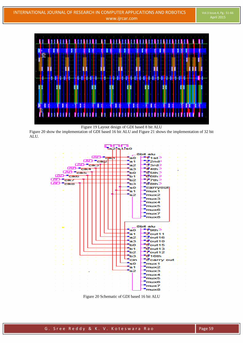
Figure 19 Layout design of GDI based 8 bit ALU
Figure 20 show the implementation of GDI based 16 bit ALU and Figure 21 shows the implementation of 32 bit
ALU.
Figure 20 Schematic of GDI based 16 bit ALU

INTERNATIONAL JOURNAL OF RESEARCH IN COMPUTER APPLICATIONS AND ROBOTICS www.ijrcar.com
Vol.3 Issue.4, Pg.: 51-66
April 2015
G . S r e e R e d d y & K . V . K o t e s w a r a R a o
Page 60
Figure 21 Schematic of GDI based 32 bit ALU
Table 3 shows the comparison analysis between Pass Transistor logic, CMOS Design and GDI Technique.
Table 4 shows the comparison power analysis for 4-bit ALU and Table 5 shows the comparison power analysis
for the 8 bit ALU. Table 6 shows the comparison power analysis for the 16 bit ALU. Table 7 shows the
comparison power analysis for the 32 bit ALU. From Figure 22 to Figure 33 shows the simulation results.
Table 3 Comparison Analysis for ALU

INTERNATIONAL JOURNAL OF RESEARCH IN COMPUTER APPLICATIONS AND ROBOTICS www.ijrcar.com
Vol.3 Issue.4, Pg.: 51-66
April 2015
G . S r e e R e d d y & K . V . K o t e s w a r a R a o
Page 61
Table 4 Analysis of Power for 4-bit ALU
Table 5 Analysis of Power for 8-bit ALU
Table 6 Analysis of Power for 16-bit ALU
Table 7 Analysis of Power for 32-bit ALU

INTERNATIONAL JOURNAL OF RESEARCH IN COMPUTER APPLICATIONS AND ROBOTICS www.ijrcar.com
Vol.3 Issue.4, Pg.: 51-66
April 2015
G . S r e e R e d d y & K . V . K o t e s w a r a R a o
Page 62
5. Simulation Results
Figure 22 Simulation results for Function F1=A‟B
From the above figure we know that „A‟ and „B‟ are two inputs and the function output expression is A`B that is
the input „A‟ is inverted and multiplied with the „B‟ input results F1 = A`B. If A = 0 and B = 1 then A` = 1 and output results „F1= 1.1 = 1‟.
Figure 23 Simulation results for Function F2=A‟+B
From the above figure we know that „A‟ and „B‟ are two inputs and the function output expression is A`+B that
is the input „A‟ is inverted and added with the „B‟ input results F2 = A`+B. If A = 1 and B = 1 then A` = 0 and
output results „F2= 0+1 = 1‟.
Figure 24 Simulation results for GDI based AND gate
From the above figure we know that „A‟ and „B‟ are two inputs and the function output expression is A.B that is
the input „A‟ is multiplied with the „B‟ input results out = A.B. If A = 1 and B = 1 then output results „out =1.1=
1‟
Figure 25 Simulation results for GDI based NOT gate
From the above figure we know that „A‟ is the input and the function output expression is A‟ that is the input „A‟ is inverted and results out = A`. If A = 1 then output results out = A` = 1` = 0.

INTERNATIONAL JOURNAL OF RESEARCH IN COMPUTER APPLICATIONS AND ROBOTICS www.ijrcar.com
Vol.3 Issue.4, Pg.: 51-66
April 2015
G . S r e e R e d d y & K . V . K o t e s w a r a R a o
Page 63
Figure 26 Simulation results for GDI based OR gate
From the above figure we know that „A‟ and „B‟ are two inputs and the function output expression is A+B that
is the input „A‟ is added with the „B‟ input results out = A+B. If A = 1 and B = 0 then output results „out =
1+0=1‟.
Figure 27 Simulation results for 2x1 Multiplexer
From the above figure we know that „A‟ and „B‟ are two inputs and „S‟ is the select input line. By using the
select input line the input „A‟ or „B‟ will be selected. If the select line „S = 0‟ then output results „out = A‟ or if
select line „S = 1‟ the output results „out = B‟.
Figure 28 Simulation results for 4x1 Multiplexer
From the above figure we know that „A‟, „B‟, „C‟ and „D‟ are four inputs and „S1‟ and „S2‟ are the two select
input lines. By using the select input line the input „A‟ or „B‟ or „C‟ or „D‟ will be selected. If the select lines
„S1 = 0‟ and „S2 = 0‟ then output results „out = A‟. If the select lines
„S1 = 0‟ and „S2 = 1‟ then output results „out = B‟. If the select lines
„S1 = 1‟ and „S2 = 0‟ then output results „out = C‟. And if the select lines „S1 = 1‟ and „S2 = 1‟ then output results „out = D‟.

INTERNATIONAL JOURNAL OF RESEARCH IN COMPUTER APPLICATIONS AND ROBOTICS www.ijrcar.com
Vol.3 Issue.4, Pg.: 51-66
April 2015
G . S r e e R e d d y & K . V . K o t e s w a r a R a o
Page 64
Figure 29 Simulation results for GDI based XOR gate
From the above figure we know that „A‟ and „B‟ are two inputs and the function output expression is A XOR B
that is the input „A‟ is XOR operated with the „B‟ input results out = A XOR B. If A = 1 and B = 0 then output results „out = 0‟.
Figure 30 Simulation results for GDI based Full Adder
From the above figure we know that „A‟, „B‟ and „Cin‟ are the three inputs and the outputs are SUM and
CARRY. SUM = A XOR B XOR Cin and CARRY = (A.B) + (B.Cin) + (Cin.A). If „A = 0‟, „B = 1‟ and „Cin =
1‟ the output „SUM = 0‟ and „CARRY = 1‟.
Figure 31 Simulation results for 4-Bit ALU by using GDI
From the above figure we shown the simulation results for 4-bit ALU having eight inputs that is „a0‟,‟a1‟, „a2‟,
„a3‟, „b0‟, „b1‟, „b2‟ and „b3‟ and four outputs for four bits. The operation will be executed according to the
table shown in the Table 2 ALU operations.

INTERNATIONAL JOURNAL OF RESEARCH IN COMPUTER APPLICATIONS AND ROBOTICS www.ijrcar.com
Vol.3 Issue.4, Pg.: 51-66
April 2015
G . S r e e R e d d y & K . V . K o t e s w a r a R a o
Page 65
Figure 32 Simulation results for 8-Bit ALU by using GDI
From the above figure we shown the simulation results for 8-bit ALU having sixteen inputs that is „a0‟,‟a1‟, „a2‟, „a3‟, „b0‟, „b1‟, „b2‟ and „b3‟ and the same inputs given to another four bit ALU. The combination of two
4-bit ALU‟S results 8-bit ALU and gives eight outputs for eight bits. The operation will be executed according
to the table shown in the Table 2 ALU operations.
Figure 33 Simulation results for 32-Bit ALU by using GDI
From the above figure we shown the simulation results for 32-bit ALU having 64 inputs that is „a0‟,‟a1‟, „a2‟,
„a3‟, „b0‟, „b1‟, „b2‟ and „b3‟ and the same inputs given to another sixteen bit ALU. The combination of two
16-bit ALU‟S results 32-bit ALU and gives 32 outputs for 32 bits. The operation will be executed according to the table shown in the Table 2 ALU operations.
6. Conclusion
32-Bit ALU is designed in transistor level with less area, less propagation delay and low power consumption by
using GDI technique. In GDI technique the number of power suppliers and ground connections are reduced so
that power required to designing the 4- bit, 8-bit, 16-bit and 32-bit ALU is less. To design ALU 2x1
multiplexers, 4x1 multiplexers and full adder circuits are used. The numbers of transistors were reduced by using the concept called GDI technique. This work presents a 4-bit, 8-bit, 16-bit and 32-bit ALU designed in
120nm technology. The power analysis is compared and shown for Pass transistor logic, CMOS logic and GDI
technique in Table 3 to Table 7. From the Table 4 to Table 7 we can say that the 4-bit, 8-bit, 16-bit and 32-bit
design by using GDI technique power dissipation is very less. To design 4- bit ALU the power dissipation is
very less when compared to other techniques were about 546.24uw. To design 8- bit ALU the power dissipation
is very less when compared to other techniques were about 899.54uw. To design 16- bit ALU the power
dissipation is very less when compared to other techniques were about 996.54uw. To design 32- bit ALU the
power dissipation is very less when compared to other techniques were about 1252.54uw. By comparing all the
analysis GDI technique were proved to have best performance with less propagation delay, low area and low
power consumption.

INTERNATIONAL JOURNAL OF RESEARCH IN COMPUTER APPLICATIONS AND ROBOTICS www.ijrcar.com
Vol.3 Issue.4, Pg.: 51-66
April 2015
G . S r e e R e d d y & K . V . K o t e s w a r a R a o
Page 66
REFERENCES
[1]. T. Esther Rani, M. Asha Rani, Dr. Rameshwar rao, “AREA OPTIMIZED LOW POWER ARITHMETIC AND
LOGIC UNIT”, 978-1-4244-8679-3/11/$26.00 ©2011 IEEE.
[2]. Morgenshtein, A., Fish, A., Wagner, I.A.: “Gate-Diffusion Input (GDI) – A Technique for Low Power
Design of Digital Circuits”: Analysis and Characterization. In: ISCAS 2002, USA (May 2002).
[3]. Saradindu Panda, N. Mohan Kumar, C.K. Sarkar., “Transistor Count Optimization of Conventional CMOS
Full Adder & Optimization of Power and Delay of New Implementation of 18 Transistor Full Adder by
Dual Threshold Node Design with Submicron Channel Length" ,in Computers and Devices for
Communication, 2009. CODEC 2009. 4th International Conference on pp: 1 – 4
[4]. L.Bisdounis, D.Gouvetas and O.Koufopavlou, “A comparative study of CMOS circuit design styles for
Low power high-speed VLSI circuits”, Int. J. of Electronics, Vol.84, No.6, pp. 599- 613, 1998. Anu Gupta,
Design Explorations of VLSI Arithmetic Circuits, Ph.D. Thesis, BITS Pilani, India, 2003.
[5]. A. P. Chandrakasan, S. Sheng, and R. W. Brodersen, “Low- power CMOS digital design”, IEEE J. Solid
State Circuits, vol. 27, pp.473–484, Apr. 1992.
[6]. A. P. Chandrakasan and R.W. Brodersen, “Minimizing power consumption in digital CMOS circuits”, Proc.
IEEE, vol. 83, pp. 498–523, Apr.1995.
G. Sree Reddy: He is currently Studying M.Tech in VLSI Design, in Sree Vidyanikethan Engineering College, Tirupati.
His areas of interest are Low Power VLSI Design.
K. V. Koteswara Rao: He is currently working as an Assistant Professor in ECE department of Sree Vidyanikethan
Engineering College, Tirupati. He has completed M.Tech in EDT, in NIT Calicut. His research areas of interest are Microelectronics, Antennas.