Embed Size (px)
Citation preview
TLV712xx
GND
EN
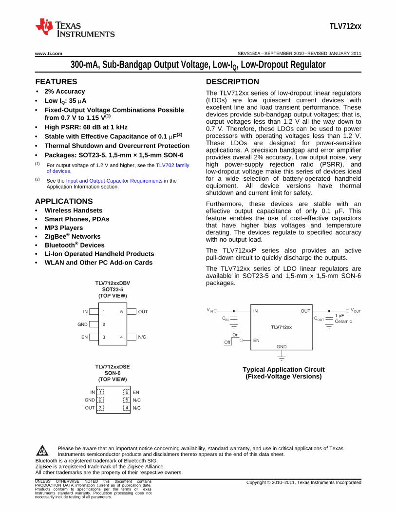
IN OUTVIN
VOUT
On
Off
CIN
COUT
1 F
Ceramic
m
TLV712xxDBV
SOT23-5
(TOP VIEW)
OUT
N/C
IN
GND
EN
1
2
3
5
4
TLV712xxDSE
SON-6
(TOP VIEW)
EN
N/C
N/C
6
5
4
IN
GND
OUT
1
2
3
TLV712xx
www.ti.com SBVS150A –SEPTEMBER 2010–REVISED JANUARY 2011
300-mA, Sub-Bandgap Output Voltage, Low-IQ, Low-Dropout Regulator
1FEATURES DESCRIPTION234• 2% Accuracy The TLV712xx series of low-dropout linear regulators
(LDOs) are low quiescent current devices with• Low IQ: 35 mAexcellent line and load transient performance. These• Fixed-Output Voltage Combinations Possibledevices provide sub-bandgap output voltages; that is,from 0.7 V to 1.15 V(1)output voltages less than 1.2 V all the way down to
• High PSRR: 68 dB at 1 kHz 0.7 V. Therefore, these LDOs can be used to powerprocessors with operating voltages less than 1.2 V.• Stable with Effective Capacitance of 0.1 mF(2)
These LDOs are designed for power-sensitive• Thermal Shutdown and Overcurrent Protectionapplications. A precision bandgap and error amplifier
• Packages: SOT23-5, 1,5-mm × 1,5-mm SON-6 provides overall 2% accuracy. Low output noise, veryhigh power-supply rejection ratio (PSRR), and(1) For output voltage of 1.2 V and higher, see the TLV702 family
of devices. low-dropout voltage make this series of devices idealfor a wide selection of battery-operated handheld(2) See the Input and Output Capacitor Requirements in theequipment. All device versions have thermalApplication Information section.shutdown and current limit for safety.
APPLICATIONS Furthermore, these devices are stable with an• Wireless Handsets effective output capacitance of only 0.1 mF. This
feature enables the use of cost-effective capacitors• Smart Phones, PDAsthat have higher bias voltages and temperature• MP3 Playersderating. The devices regulate to specified accuracy
• ZigBee® Networks with no output load.• Bluetooth® Devices
The TLV712xxP series also provides an active• Li-Ion Operated Handheld Productspull-down circuit to quickly discharge the outputs.
• WLAN and Other PC Add-on CardsThe TLV712xx series of LDO linear regulators areavailable in SOT23-5 and 1,5-mm x 1,5-mm SON-6packages.
Typical Application Circuit(Fixed-Voltage Versions)
1
Please be aware that an important notice concerning availability, standard warranty, and use in critical applications of TexasInstruments semiconductor products and disclaimers thereto appears at the end of this data sheet.
2Bluetooth is a registered trademark of Bluetooth SIG.3ZigBee is a registered trademark of the ZigBee Alliance.4All other trademarks are the property of their respective owners.
UNLESS OTHERWISE NOTED this document contains Copyright © 2010–2011, Texas Instruments IncorporatedPRODUCTION DATA information current as of publication date.Products conform to specifications per the terms of TexasInstruments standard warranty. Production processing does notnecessarily include testing of all parameters.
TLV712xx
SBVS150A –SEPTEMBER 2010–REVISED JANUARY 2011 www.ti.com
This integrated circuit can be damaged by ESD. Texas Instruments recommends that all integrated circuits be handled withappropriate precautions. Failure to observe proper handling and installation procedures can cause damage.
ESD damage can range from subtle performance degradation to complete device failure. Precision integrated circuits may be moresusceptible to damage because very small parametric changes could cause the device not to meet its published specifications.
ORDERING INFORMATION (1)
PRODUCT VOUT(2)
TLV712xx(x)Pyyyz XX(X) is the nominal output voltage. For output voltages with a resolution of 100 mV, twodigits are used in the ordering number; otherwise, three digits are used (for example, 09 =0.9 V; 085 = 0.85 V).P is optional; devices with P have an LDO regulator with an active output discharge.YYY is the package designator.Z is package quantity. Use "R" for reel (3000 pieces), and "T" for tape (250 pieces).
(1) For the most current package and ordering information see the Package Option Addendum at the end of this document, or visit thedevice product folder at www.ti.com.
(2) Output voltages from 0.7 V to 1.15 V in 50-mV increments are available. Contact factory for details and availability.
ABSOLUTE MAXIMUM RATINGSover operating free-air temperature range (unless otherwise noted) (1)
VALUE UNIT
MIN MAX
IN –0.3 +6.0 V
Voltage (2) EN –0.3 +6.0 V
OUT –0.3 +5.0 V
Current (source) OUT Internally limited
Output short-circuit duration Indefinite
Operating junction, TJ –55 +150 °CTemperature
Storage, Tstg –55 +150 °C
Human body model (HBM) QSS 009-105 (JESD22-A114A) 2 kVElectrostatic Discharge Rating (3)
Charged device model (CDM) QSS 009-147 500 V(JESD22-C101B.01)
(1) Stresses beyond those listed under absolute maximum ratings may cause permanent damage to the device. These are stress ratingsonly, and functional operation of the device at these or any other conditions beyond those indicated under recommended operatingconditions is not implied. Exposure to absolute-maximum-rated conditions for extended periods my affect device reliability.
(2) All voltages are with respect to network ground terminal.(3) ESD testing is performed according to the respective JESD22 JEDEC standard.
DISSIPATION RATINGS (1)
PACKAGE RqJA TA < +25°C TA = +70°C TA = +85°C
DBV 200°C/W 500 mW 275 mW 200 mW
DSE 180°C/W 555 mW 305 mW 222 mW
(1) For board details, see the Thermal Information section.
2 Submit Documentation Feedback Copyright © 2010–2011, Texas Instruments Incorporated
TLV712xx
www.ti.com SBVS150A –SEPTEMBER 2010–REVISED JANUARY 2011
ELECTRICAL CHARACTERISTICSAt VIN = 2.0 V, IOUT = 10 mA, VEN = 0.9 V, COUT = 1.0 mF, and TJ = –40°C to +125°C, unless otherwise noted. Typical valuesare at TJ = +25°C.SPACE
PARAMETER TEST CONDITIONS MIN TYP MAX UNIT
VIN Input voltage range 2.0 5.5 V
VOUT DC output accuracy –20 6 +20 mV
ΔVO/ΔVIN Line regulation 2 V ≤ VIN ≤ 5.5 V, 1 5 mV
ΔVO/ΔIOUT Load regulation 0 mA ≤ IOUT ≤ 300 mA 1 15 mV
ICL Output current limit VOUT = 0.9 × VOUT(NOM) 320 500 860 mA
IOUT = 0 mA 35 55 mAIGND Ground pin current
IOUT = 300 mA 370 mA
VEN ≤ 0.4 V 400 nAISHDN Ground pin current (shutdown) VEN ≤ 0.4 V, 2.0 V ≤ VIN ≤ 4.5 V, 1 2 mATJ = –40°C to +85°C
PSRR Power-supply rejection ratio f = 1 kHz 68 dB
BW = 100 Hz to 100 kHz,VN Output noise voltage 30 mVRMSVOUT = 0.7 V
tSTR Startup time (1) IOUT = 300 mA 100 ms
VEN(HI) Enable pin high (enabled) 0.9 VIN V
VEN(LO) Enable pin low (disabled) 0 0.4 V
IEN Enable pin current VIN = VEN = 5.5 V 0.04 mA
UVLO Undervoltage lockout VIN rising 1.9 V
Active pull-down resistanceRDISCHARGE VEN = 0 V 120 Ω(TLV712xxP only)
Shutdown, temperature increasing +165 °CTSD Thermal shutdown temperature
Reset, temperature decreasing +145 °C
TJ Operating junction temperature –40 +125 °C
(1) Startup time = time from EN assertion to 0.98 × VOUT(NOM).
Copyright © 2010–2011, Texas Instruments Incorporated Submit Documentation Feedback 3
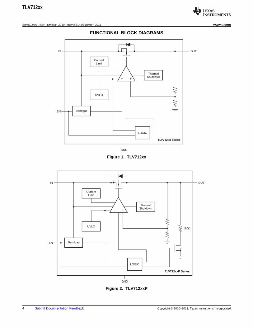
ThermalShutdown
CurrentLimit
UVLO
Bandgap
IN
EN
OUT
LOGIC
GND
TLV712xx Series
ThermalShutdown
CurrentLimit
UVLO
Bandgap
IN
EN
OUT
LOGIC
GND
TLV712xxP Series
120W
TLV712xx
SBVS150A –SEPTEMBER 2010–REVISED JANUARY 2011 www.ti.com
FUNCTIONAL BLOCK DIAGRAMS
Figure 1. TLV712xx
Figure 2. TLV712xxP
4 Submit Documentation Feedback Copyright © 2010–2011, Texas Instruments Incorporated
EN
N/C
N/C
6
5
4
IN
GND
OUT
1
2
3
OUT
NC
IN
GND
EN
1
2
3
5
4
TLV712xx
www.ti.com SBVS150A –SEPTEMBER 2010–REVISED JANUARY 2011
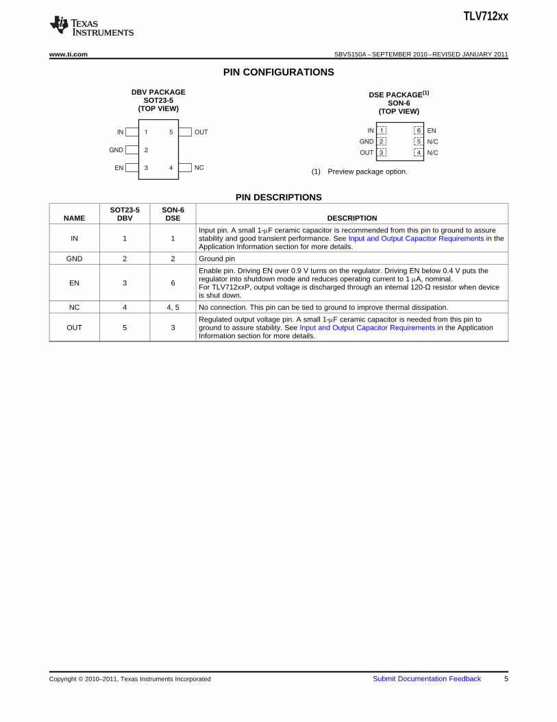
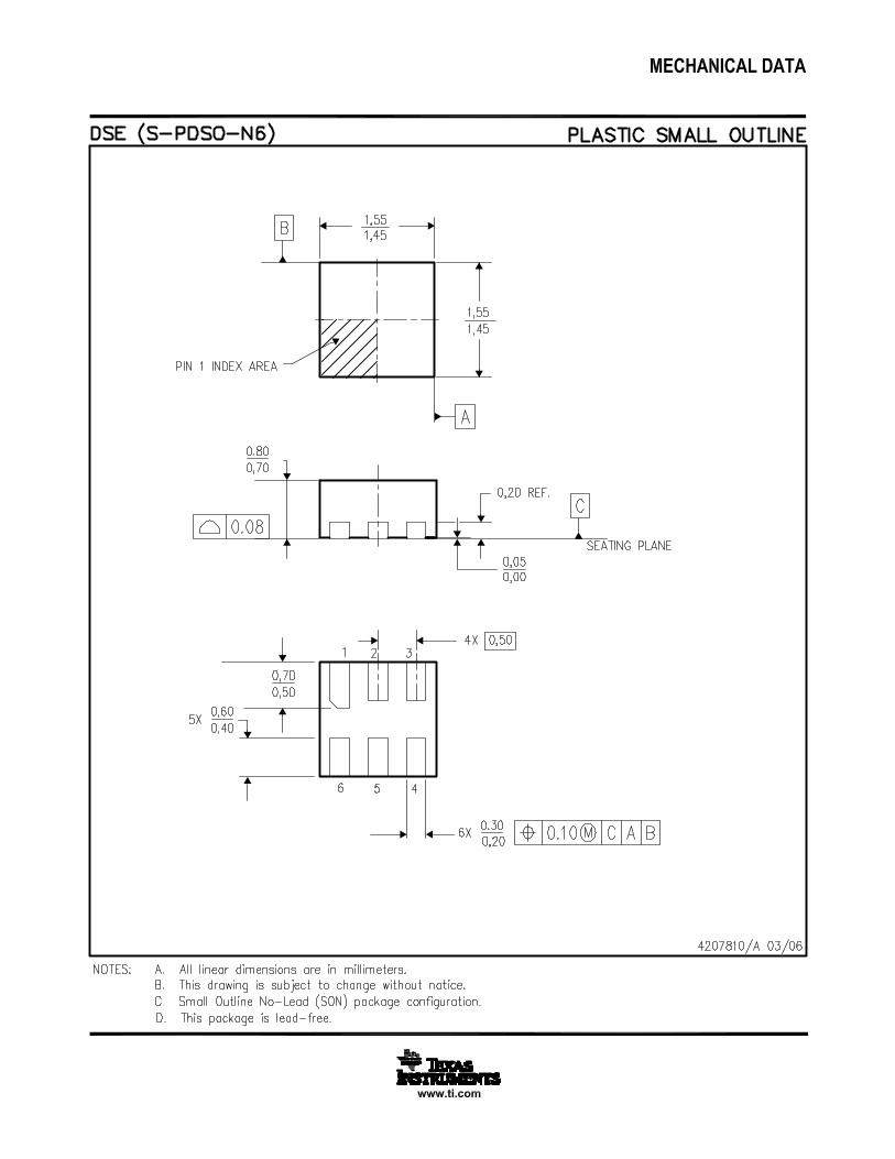
PIN CONFIGURATIONS
DBV PACKAGE DSE PACKAGE(1)
SOT23-5 SON-6(TOP VIEW) (TOP VIEW)
(1) Preview package option.
PIN DESCRIPTIONSSOT23-5 SON-6
NAME DBV DSE DESCRIPTION
Input pin. A small 1-mF ceramic capacitor is recommended from this pin to ground to assureIN 1 1 stability and good transient performance. See Input and Output Capacitor Requirements in the
Application Information section for more details.
GND 2 2 Ground pin
Enable pin. Driving EN over 0.9 V turns on the regulator. Driving EN below 0.4 V puts theregulator into shutdown mode and reduces operating current to 1 mA, nominal.EN 3 6 For TLV712xxP, output voltage is discharged through an internal 120-Ω resistor when deviceis shut down.
NC 4 4, 5 No connection. This pin can be tied to ground to improve thermal dissipation.
Regulated output voltage pin. A small 1-mF ceramic capacitor is needed from this pin toOUT 5 3 ground to assure stability. See Input and Output Capacitor Requirements in the Application
Information section for more details.
Copyright © 2010–2011, Texas Instruments Incorporated Submit Documentation Feedback 5
0.80
0.78
0.76
0.74
0.72
0.70
0.68
0.66
0.64
0.62
0.60
VO
UT
(V)
2 2.5 3 3.5 4 4.5 5
V (V)IN
5.5
+125 C°
+85 C°
+25 C°
-40 C°
V = 0.7 VOUT
0 100 150 300
I (mA)OUT
0.80
0.78
0.76
0.74
0.72
0.70
0.68
0.66
0.64
0.62
0.60
V(V
)O
UT
50 200
+125 C°
+85 C°
+25 C°
-40 C°
250
V = 0.7 VOUT
V(V
)O
UT
-40 -25 -10 5 20 35 50 65 80 95 110
Temperature ( C)°
125
10mA
150mA
300mA
0.80
0.78
0.76
0.74
0.72
0.70
0.68
0.66
0.64
0.62
0.60
V = 0.7 VOUT
50
45
40
35
30
25
20
15
10
5
0
I GN
D(
Am
)
2 2.5 3 3.5 4 4..5 5
V (V)IN
5.5
+125 C°
+85 C°
+25 C°
-40 C°
V = 0.7 VOUT
350
300
250
200
150
100
50
0
I GN
D(m
A)
0
I (mA)OUT
300
+125 C°
+85 C°
+25 C°
-40 C°
V = 0.7 VOUT
50 150 250100 200
50
45
40
35
30
25
20
15
10
5
0
I(
A)
mG
ND
-40 -25 -10 5 20 35 50 65 80 95 110
Temperature ( C)°
125
V = 0.7 VOUT
TLV712xx
SBVS150A –SEPTEMBER 2010–REVISED JANUARY 2011 www.ti.com
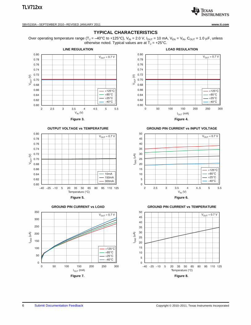
TYPICAL CHARACTERISTICSOver operating temperature range (TJ = –40°C to +125°C), VIN = 2.0 V, IOUT = 10 mA, VEN = VIN, COUT = 1.0 mF, unless
otherwise noted. Typical values are at TJ = +25°C.
LINE REGULATION LOAD REGULATION
Figure 3. Figure 4.
OUTPUT VOLTAGE vs TEMPERATURE GROUND PIN CURRENT vs INPUT VOLTAGE
Figure 5. Figure 6.
GROUND PIN CURRENT vs LOAD GROUND PIN CURRENT vs TEMPERATURE
Figure 7. Figure 8.
6 Submit Documentation Feedback Copyright © 2010–2011, Texas Instruments Incorporated
2.5
2
1.5
1
0.5
0
I SH
DN
(A
m)
2 2.5 3 3.5 4 4.5 5
V (V)IN
5.5
+125 C°
+85 C°
+25 C°
-40 C°
V = 0.7 VOUT
700
600
500
400
300
200
100
0
I LIM
(mA
)
2 2.5 3 3.5 4 4.5 5
V (V)IN
5.5
V = 0.7 VOUT
+85 C°
+25 C°
-40 C°
10
1
0.1
0.01
0.001
Ou
tpu
t S
pe
ctr
al N
ois
e D
en
sity (
V/
)m
ÖH
z
10 100 1 k 10 k 100 k 1 M 10 M
Frequency (Hz)
V = 0.7 VOUT
C = C = 1 FmIN OUT
100
90
80
70
60
50
40
30
20
10
0
PS
RR
(d
B)
10 100 1 k 10 k 100 k 1 M 10 M
Frequency (Hz)
I = 150 mAOUT
I = 10 mAOUT
10
mA
/div
10
mV
/div
20 s/divm
VOUT
V
t = t = 1 s
OUT
R F
= 0.7 V
m
IOUT
15 mA
0 mA
50
mA
/div
20
mV
/div
20 s/divm
VOUT
IOUT
70 mA
0 mA
V
t = t = 1 s
OUT
R F
= 0.7 V
m
TLV712xx
www.ti.com SBVS150A –SEPTEMBER 2010–REVISED JANUARY 2011
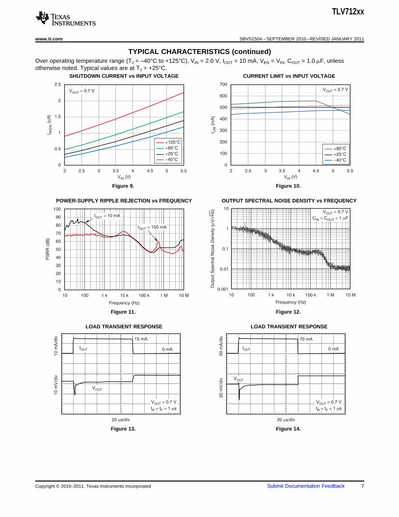
TYPICAL CHARACTERISTICS (continued)Over operating temperature range (TJ = –40°C to +125°C), VIN = 2.0 V, IOUT = 10 mA, VEN = VIN, COUT = 1.0 mF, unlessotherwise noted. Typical values are at TJ = +25°C.
SHUTDOWN CURRENT vs INPUT VOLTAGE CURRENT LIMIT vs INPUT VOLTAGE
Figure 9. Figure 10.
POWER-SUPPLY RIPPLE REJECTION vs FREQUENCY OUTPUT SPECTRAL NOISE DENSITY vs FREQUENCY
Figure 11. Figure 12.
LOAD TRANSIENT RESPONSE LOAD TRANSIENT RESPONSE
Figure 13. Figure 14.
Copyright © 2010–2011, Texas Instruments Incorporated Submit Documentation Feedback 7
1 V
/div
2 m
V/d
iv
1 ms/div
VOUT
Slew Rate = 1 V/ sm
VIN
2.9 V
2.3 V
V = 0.7 V
I 300 mA
OUT
OUT =
20
0 m
A/d
iv5
0 m
V/d
iv
20 s/divm
VOUT
300 mA
0 mAIOUT
V
t = t = 1 s
OUT
R F
= 0.7 V
m
2 V
/div
10
mV
/div
1 ms/div
Slew Rate = 1 V/ sm
V = 0.7 V
I = 300 mA
OUT
OUT5.5 V
VIN2.0 V
VOUT
1 V
/div
100 ms/div
VOUT
VIN
V = 0.7 VOUT
I 1 mAOUT =
TLV712xx
SBVS150A –SEPTEMBER 2010–REVISED JANUARY 2011 www.ti.com
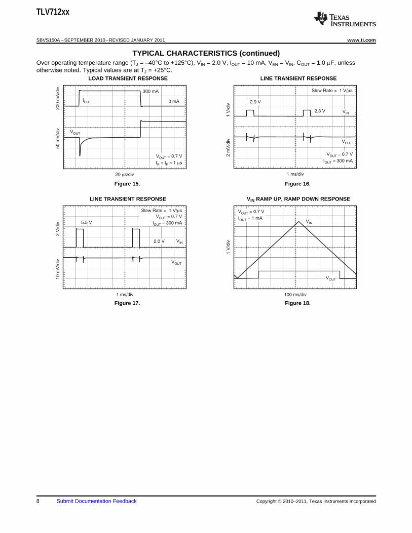
TYPICAL CHARACTERISTICS (continued)Over operating temperature range (TJ = –40°C to +125°C), VIN = 2.0 V, IOUT = 10 mA, VEN = VIN, COUT = 1.0 mF, unlessotherwise noted. Typical values are at TJ = +25°C.
LOAD TRANSIENT RESPONSE LINE TRANSIENT RESPONSE
Figure 15. Figure 16.
LINE TRANSIENT RESPONSE VIN RAMP UP, RAMP DOWN RESPONSE
Figure 17. Figure 18.
8 Submit Documentation Feedback Copyright © 2010–2011, Texas Instruments Incorporated
t =(120 R )
(120 + R )L
L
·
· COUT
TLV712xx
www.ti.com SBVS150A –SEPTEMBER 2010–REVISED JANUARY 2011
APPLICATION INFORMATION
GENERAL DESCRIPTION BOARD LAYOUT RECOMMENDATIONS TOIMPROVE PSRR AND NOISE PERFORMANCE
The TLV712xx belongs to a new family ofnext-generation value LDO regulators. These devices Input and output capacitors should be placed asoffer sub-bandgap output voltages; that is, output close to the device pins as possible. To improve acvoltages from 1.2 V all the way down to 0.7 V. These performance such as PSRR, output noise, anddevices consume low quiescent current and deliver transient response, it is recommended that the boardexcellent line and load transient performance. These be designed with separate ground planes for VIN andcharacteristics, combined with low noise and very VOUT, with the ground plane connected only at thegood PSRR with little (VIN – VOUT) headroom, make GND pin of the device. In addition, the groundthis family of devices ideal for portable RF connection for the output capacitor should beapplications. This family of regulators offers current connected directly to the GND pin of the device. Highlimit and thermal protection, and is specified from ESR capacitors may degrade PSRR performance.–40°C to +125°C.
INTERNAL CURRENT LIMITINPUT AND OUTPUT CAPACITOR
The TLV712xx internal current limit helps to protectREQUIREMENTSthe regulator during fault conditions. During current
1.0-mF X5R- and X7R-type ceramic capacitors are limit, the output sources a fixed amount of currentrecommended because these capacitors have that is largely independent of the output voltage. Inminimal variation in value and equivalent series such a case, the output voltage is not regulated, andresistance (ESR) over temperature. is VOUT = ILIMIT × RLOAD. The PMOS pass transistor
dissipates (VIN – VOUT) × ILIMIT until thermal shutdownHowever, the TLV712xx is designed to be stable with is triggered and the device turns off. As the devicean effective capacitance of 0.1 mF or larger at the cools, it is turned on by the internal thermal shutdownoutput. Thus, the device is stable with capacitors of circuit. If the fault condition continues, the deviceother dielectric types as well, as long as the effective cycles between current limit and thermal shutdown.capacitance under operating bias voltage and See the Thermal Information section for more details.temperature is greater than 0.1 mF. This effectivecapacitance refers to the capacitance that the LDO The PMOS pass element in the TLV712xx has asees under operating bias voltage and temperature built-in body diode that conducts current when theconditions; that is, the capacitance after taking both voltage at OUT exceeds the voltage at IN. Thisbias voltage and temperature derating into current is not limited, so if extended reverse voltageconsideration. In addition to allowing the use of operation is anticipated, external limiting to 5% of thelower-cost dielectrics, this capability of being stable rated output current is recommended.with 0.1-mF effective capacitance also enables theuse of smaller footprint capacitors that have higher SHUTDOWNderating in size- and space-constrained applications.
The enable pin (EN) is active high. The device isNOTE: Using a 0.1-mF rated capacitor at the output enabled when voltage at EN pin goes above 0.9 V.of the LDO does not ensure stability because the This relatively lower voltage value required to turn oneffective capacitance under the specified operating the LDO can also be used to power the device whenconditions would be less than 0.1 mF. Maximum ESR it is connected to a GPIO of a newer processor,should be less than 200 mΩ. where the GPIO Logic 1 voltage level is lower than
that of traditional microcontrollers. The device isAlthough an input capacitor is not required forturned off when the EN pin is held at less than 0.4 V.stability, it is good analog design practice to connectWhen shutdown capability is not required, EN can bea 0.1-mF to 1.0-mF, low ESR capacitor across the INconnected to the IN pin.pin and GND pin of the regulator. This capacitor
counteracts reactive input sources and improves The TLV712xxP version has internal active pull-downtransient response, noise rejection, and ripple circuitry that discharges the output with a timerejection. A higher-value capacitor may be necessary constant of:if large, fast rise-time load transients are anticipated,or if the device is not located close to the powersource. If source impedance is more than 2 Ω, a0.1-mF input capacitor may be necessary to ensure where:stability.
• RL = Load resistance• COUT = Output capacitor (1)
Copyright © 2010–2011, Texas Instruments Incorporated Submit Documentation Feedback 9
P = (V V ) I- ´D IN OUT OUT
TLV712xx
SBVS150A –SEPTEMBER 2010–REVISED JANUARY 2011 www.ti.com
DROPOUT VOLTAGE The internal protection circuitry of the TLV712xx hasbeen designed to protect against overload conditions.
The TLV712xx uses a PMOS pass transistor to It was not intended to replace proper heatsinking.achieve low dropout. For the complete output voltage Continuously running the TLV712xx into thermalrange of 0.7 V to 1.2 V, the device can supply 300 shutdown degrades device reliability.mA with a rated minimum input voltage of 2.0 V. Notethat the dropout voltage specification is not relevant POWER DISSIPATIONfor the TLV712xx family of devices because theoutput voltage range of the device does not exceed The ability to remove heat from the die is different for1.2 V and the minimum input voltage for the device is each package type, presenting different2.0 V. considerations in the printed circuit board (PCB)
layout. The PCB area around the device that is freeTRANSIENT RESPONSE of other components moves the heat from the device
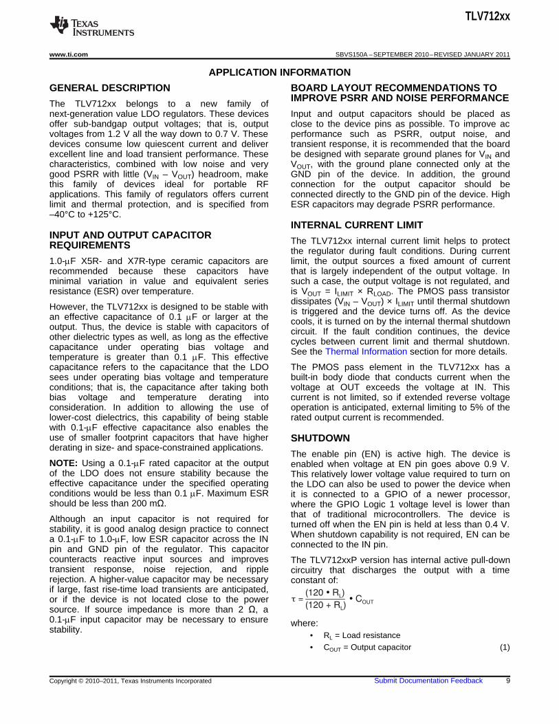
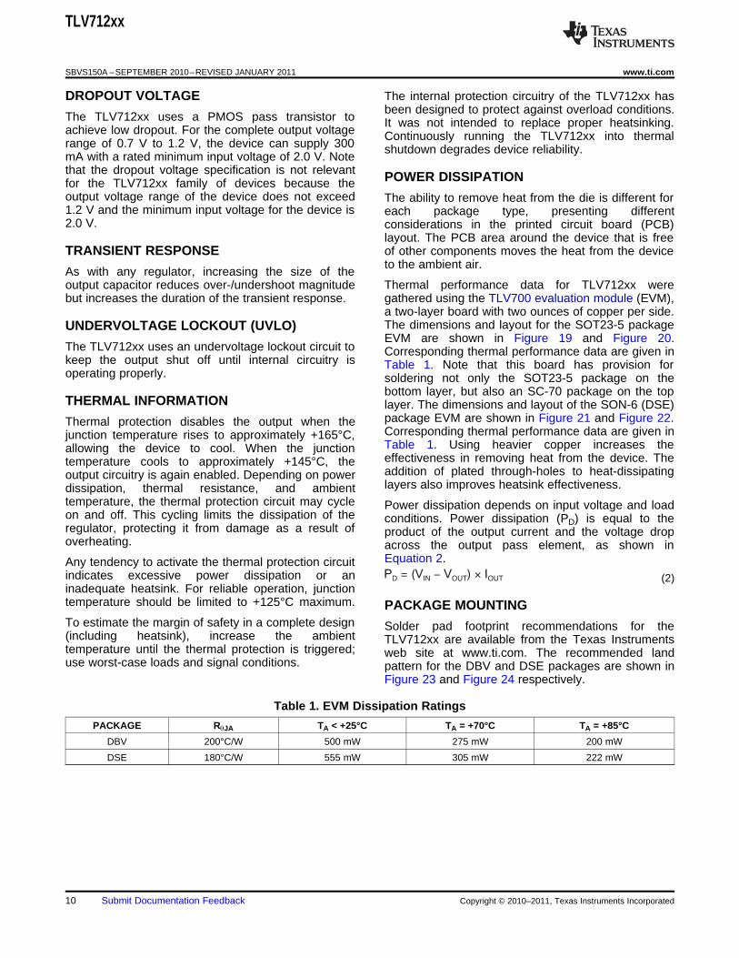
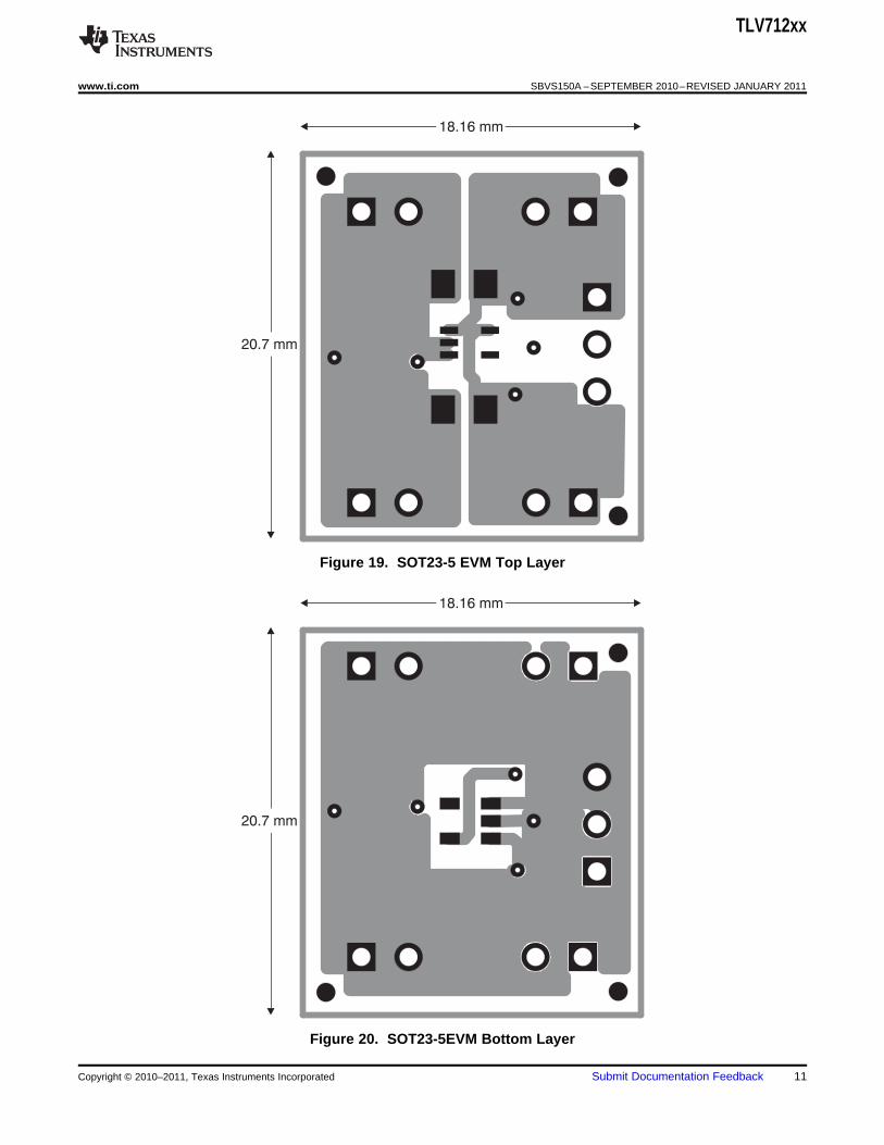
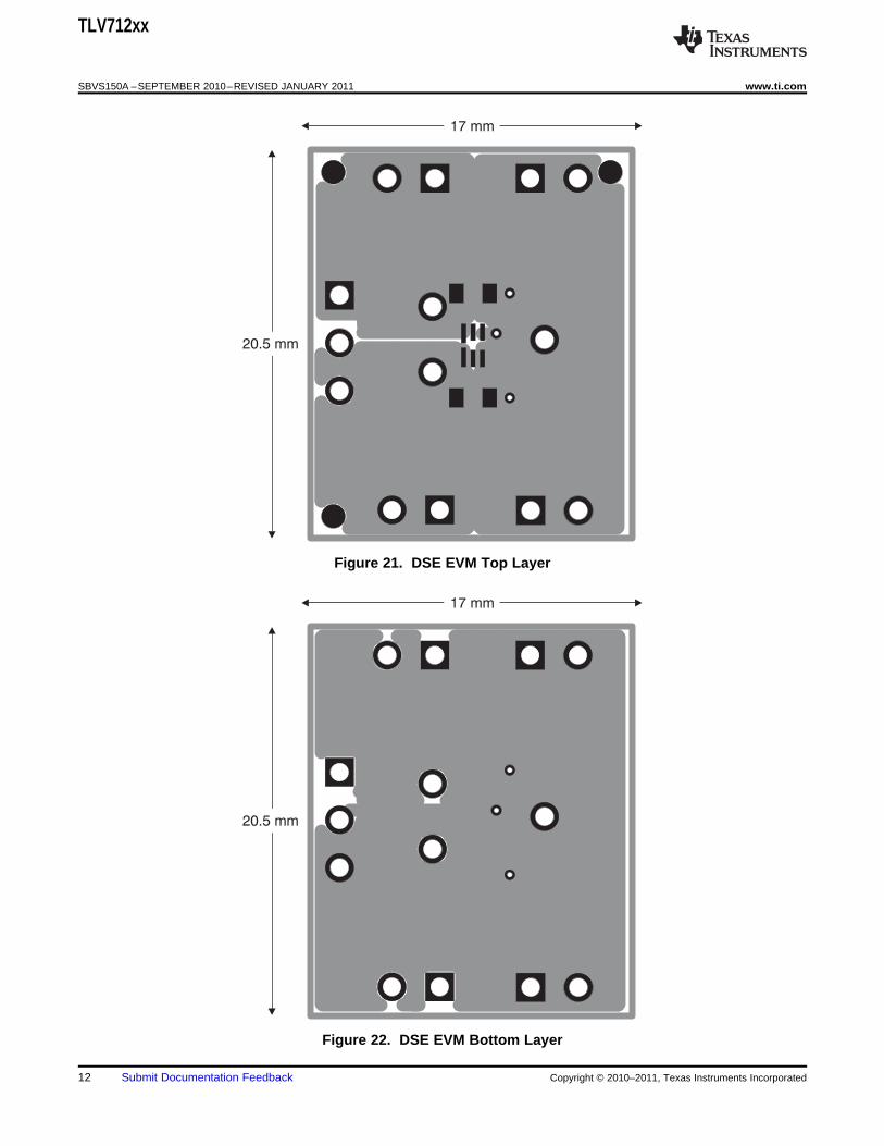
to the ambient air.As with any regulator, increasing the size of theoutput capacitor reduces over-/undershoot magnitude Thermal performance data for TLV712xx werebut increases the duration of the transient response. gathered using the TLV700 evaluation module (EVM),
a two-layer board with two ounces of copper per side.The dimensions and layout for the SOT23-5 packageUNDERVOLTAGE LOCKOUT (UVLO)EVM are shown in Figure 19 and Figure 20.
The TLV712xx uses an undervoltage lockout circuit to Corresponding thermal performance data are given inkeep the output shut off until internal circuitry is Table 1. Note that this board has provision foroperating properly. soldering not only the SOT23-5 package on the
bottom layer, but also an SC-70 package on the topTHERMAL INFORMATION layer. The dimensions and layout of the SON-6 (DSE)
package EVM are shown in Figure 21 and Figure 22.Thermal protection disables the output when theCorresponding thermal performance data are given injunction temperature rises to approximately +165°C,Table 1. Using heavier copper increases theallowing the device to cool. When the junctioneffectiveness in removing heat from the device. Thetemperature cools to approximately +145°C, theaddition of plated through-holes to heat-dissipatingoutput circuitry is again enabled. Depending on powerlayers also improves heatsink effectiveness.dissipation, thermal resistance, and ambient
temperature, the thermal protection circuit may cycle Power dissipation depends on input voltage and loadon and off. This cycling limits the dissipation of the conditions. Power dissipation (PD) is equal to theregulator, protecting it from damage as a result of product of the output current and the voltage dropoverheating. across the output pass element, as shown in
Equation 2.Any tendency to activate the thermal protection circuitindicates excessive power dissipation or an (2)inadequate heatsink. For reliable operation, junctiontemperature should be limited to +125°C maximum. PACKAGE MOUNTINGTo estimate the margin of safety in a complete design Solder pad footprint recommendations for the(including heatsink), increase the ambient TLV712xx are available from the Texas Instrumentstemperature until the thermal protection is triggered; web site at www.ti.com. The recommended landuse worst-case loads and signal conditions. pattern for the DBV and DSE packages are shown in
Figure 23 and Figure 24 respectively.
Table 1. EVM Dissipation Ratings
PACKAGE RqJA TA < +25°C TA = +70°C TA = +85°C
DBV 200°C/W 500 mW 275 mW 200 mW
DSE 180°C/W 555 mW 305 mW 222 mW
10 Submit Documentation Feedback Copyright © 2010–2011, Texas Instruments Incorporated
18.16 mm
20.7 mm
18.16 mm
20.7 mm
TLV712xx
www.ti.com SBVS150A –SEPTEMBER 2010–REVISED JANUARY 2011
Figure 19. SOT23-5 EVM Top Layer
Figure 20. SOT23-5EVM Bottom Layer
Copyright © 2010–2011, Texas Instruments Incorporated Submit Documentation Feedback 11
17 mm
20.5 mm
17 mm
20.5 mm
TLV712xx
SBVS150A –SEPTEMBER 2010–REVISED JANUARY 2011 www.ti.com
Figure 21. DSE EVM Top Layer
Figure 22. DSE EVM Bottom Layer
12 Submit Documentation Feedback Copyright © 2010–2011, Texas Instruments Incorporated
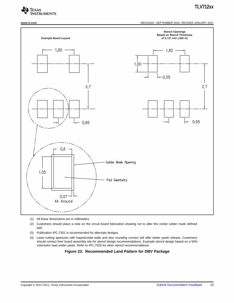
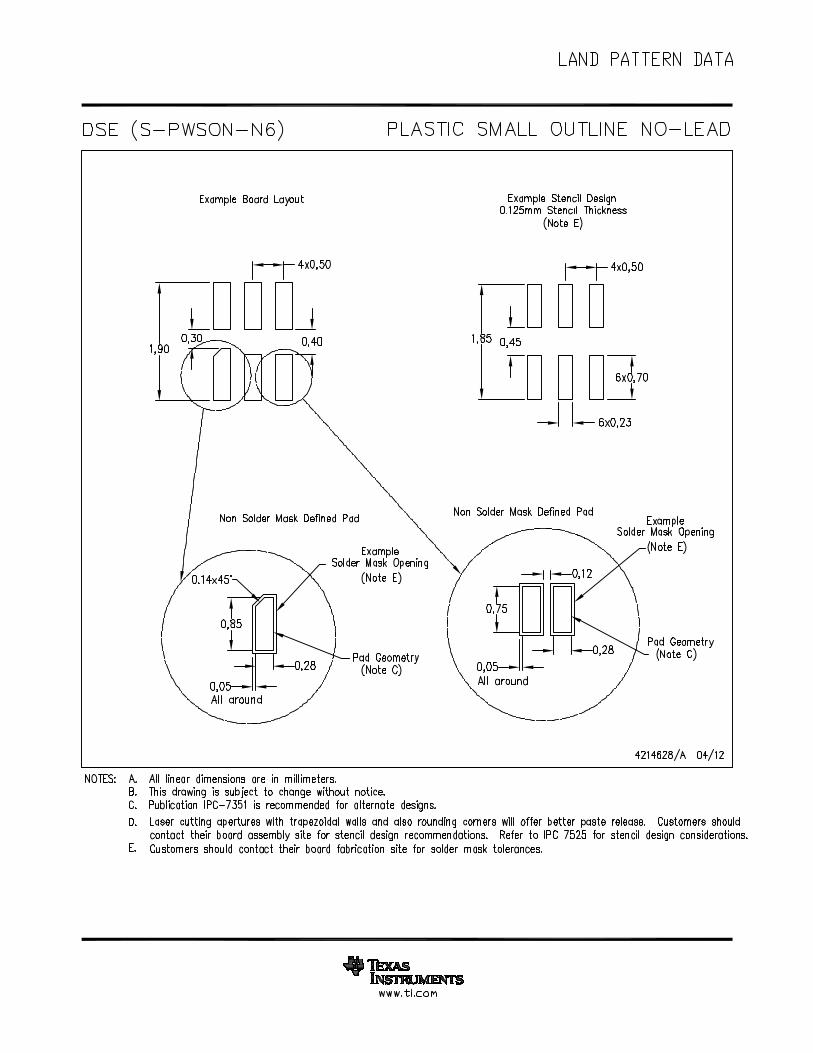
Example Board Layout
Stencil Openings
Based on Stencil Thickness
of 0,127 mm (.005 in)
TLV712xx
www.ti.com SBVS150A –SEPTEMBER 2010–REVISED JANUARY 2011
(1) All linear dimensions are in millimeters.
(2) Customers should place a note on the circuit board fabrication drawing not to alter the center solder mask definedpad.
(3) Publication IPC-7351 is recommended for alternate designs.
(4) Laser-cutting apertures with trapedzoidal walls and also rounding corners will offer better paste release. Customersshould contact their board assembly site for stencil design recommendations. Example stencil design based on a 50%volumetric load solder paste. Refer to IPC-7525 for other stencil recommendations.
Figure 23. Recommended Land Pattern for DBV Package
Copyright © 2010–2011, Texas Instruments Incorporated Submit Documentation Feedback 13
TLV712xx
SBVS150A –SEPTEMBER 2010–REVISED JANUARY 2011 www.ti.com
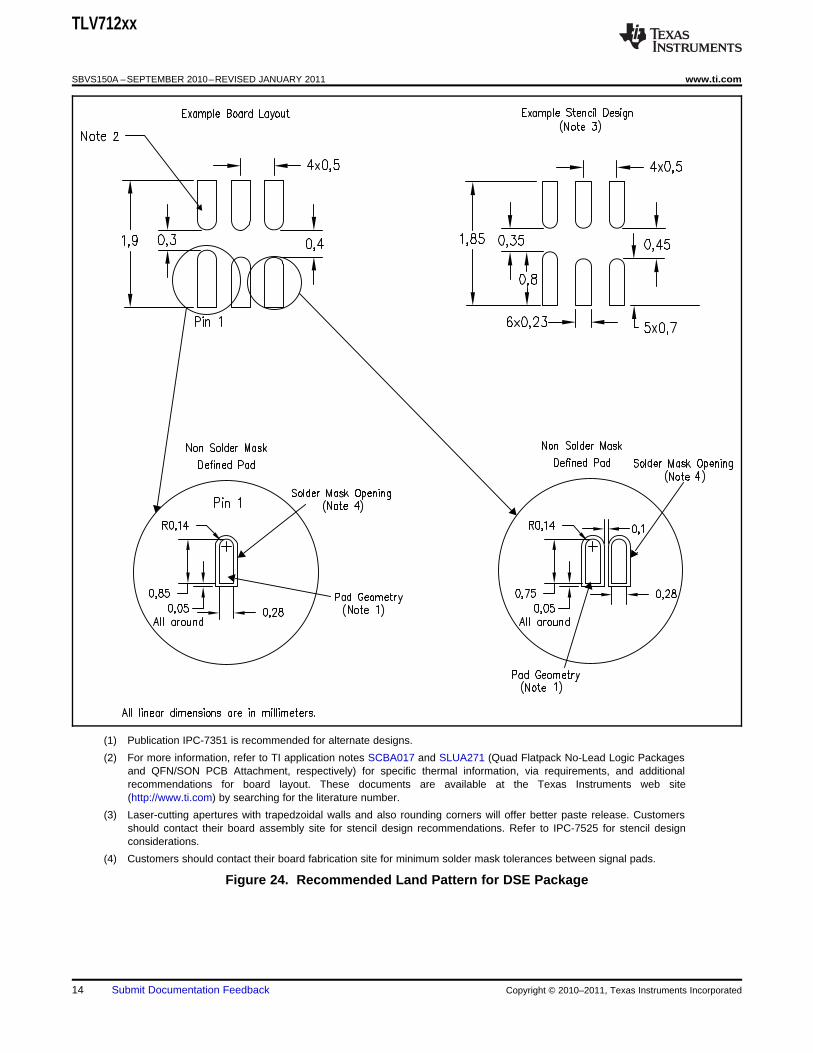
(1) Publication IPC-7351 is recommended for alternate designs.
(2) For more information, refer to TI application notes SCBA017 and SLUA271 (Quad Flatpack No-Lead Logic Packagesand QFN/SON PCB Attachment, respectively) for specific thermal information, via requirements, and additionalrecommendations for board layout. These documents are available at the Texas Instruments web site(http://www.ti.com) by searching for the literature number.
(3) Laser-cutting apertures with trapedzoidal walls and also rounding corners will offer better paste release. Customersshould contact their board assembly site for stencil design recommendations. Refer to IPC-7525 for stencil designconsiderations.
(4) Customers should contact their board fabrication site for minimum solder mask tolerances between signal pads.
Figure 24. Recommended Land Pattern for DSE Package
14 Submit Documentation Feedback Copyright © 2010–2011, Texas Instruments Incorporated
TLV712xx
www.ti.com SBVS150A –SEPTEMBER 2010–REVISED JANUARY 2011
REVISION HISTORY
NOTE: Page numbers for previous revisions may differ from page numbers in the current version.
Changes from Original (September, 2010) to Revision A Page
• Added SON package description to Features list ................................................................................................................. 1
• Added SON-6 package (preview) pin drawing to front page ................................................................................................ 1
• Revised last paragraph of Description section to include information about DSE package ................................................. 1
• Updated Ordering Information table ..................................................................................................................................... 2
• Revised Dissipation Ratings table to show DSE package information ................................................................................. 2
• Added DSE package pinout (preview) and pin configuration information ............................................................................ 5
• Updated Package Mounting and Power Dissipation sections to reflect DSE package information ................................... 10
• Added Figure 21 and Figure 22 .......................................................................................................................................... 12
• Added Figure 24 ................................................................................................................................................................. 14
Copyright © 2010–2011, Texas Instruments Incorporated Submit Documentation Feedback 15
PACKAGE OPTION ADDENDUM
www.ti.com 23-Aug-2016
Addendum-Page 1
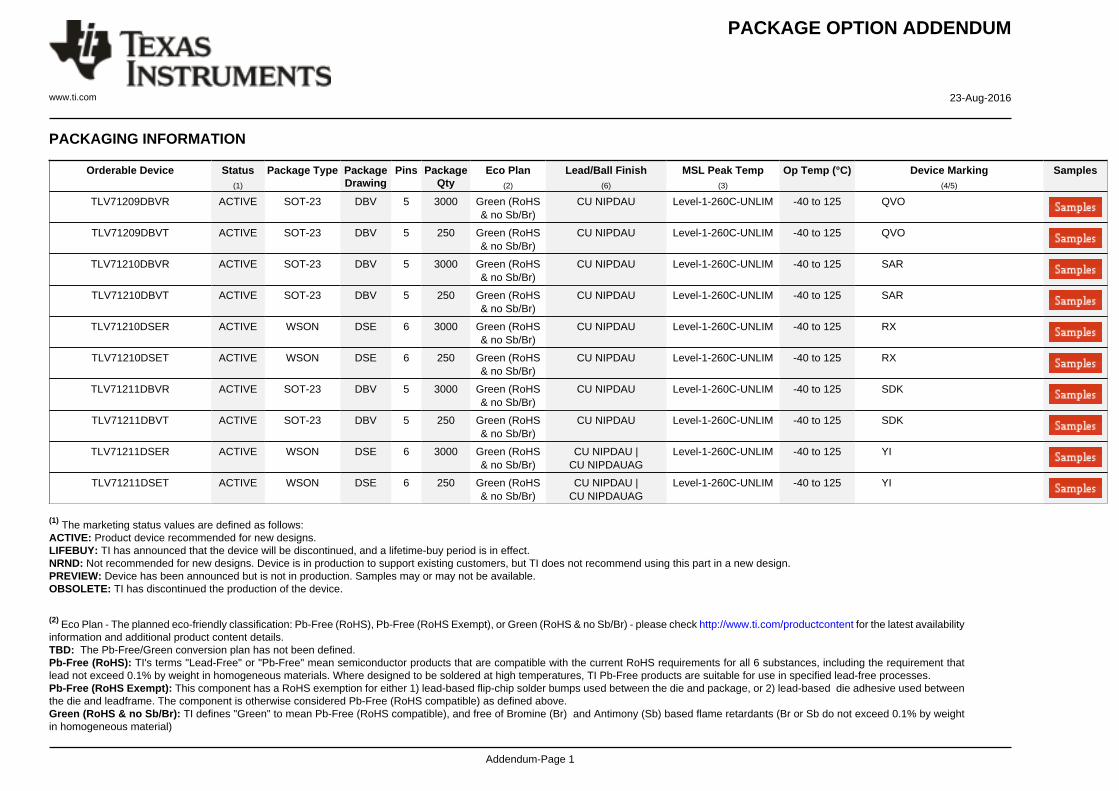
PACKAGING INFORMATION
Orderable Device Status(1)
Package Type PackageDrawing
Pins PackageQty
Eco Plan(2)
Lead/Ball Finish(6)
MSL Peak Temp(3)
Op Temp (°C) Device Marking(4/5)
Samples
TLV71209DBVR ACTIVE SOT-23 DBV 5 3000 Green (RoHS& no Sb/Br)
CU NIPDAU Level-1-260C-UNLIM -40 to 125 QVO
TLV71209DBVT ACTIVE SOT-23 DBV 5 250 Green (RoHS& no Sb/Br)
CU NIPDAU Level-1-260C-UNLIM -40 to 125 QVO
TLV71210DBVR ACTIVE SOT-23 DBV 5 3000 Green (RoHS& no Sb/Br)
CU NIPDAU Level-1-260C-UNLIM -40 to 125 SAR
TLV71210DBVT ACTIVE SOT-23 DBV 5 250 Green (RoHS& no Sb/Br)
CU NIPDAU Level-1-260C-UNLIM -40 to 125 SAR
TLV71210DSER ACTIVE WSON DSE 6 3000 Green (RoHS& no Sb/Br)
CU NIPDAU Level-1-260C-UNLIM -40 to 125 RX
TLV71210DSET ACTIVE WSON DSE 6 250 Green (RoHS& no Sb/Br)
CU NIPDAU Level-1-260C-UNLIM -40 to 125 RX
TLV71211DBVR ACTIVE SOT-23 DBV 5 3000 Green (RoHS& no Sb/Br)
CU NIPDAU Level-1-260C-UNLIM -40 to 125 SDK
TLV71211DBVT ACTIVE SOT-23 DBV 5 250 Green (RoHS& no Sb/Br)
CU NIPDAU Level-1-260C-UNLIM -40 to 125 SDK
TLV71211DSER ACTIVE WSON DSE 6 3000 Green (RoHS& no Sb/Br)
CU NIPDAU |CU NIPDAUAG
Level-1-260C-UNLIM -40 to 125 YI
TLV71211DSET ACTIVE WSON DSE 6 250 Green (RoHS& no Sb/Br)
CU NIPDAU |CU NIPDAUAG
Level-1-260C-UNLIM -40 to 125 YI
(1) The marketing status values are defined as follows:ACTIVE: Product device recommended for new designs.LIFEBUY: TI has announced that the device will be discontinued, and a lifetime-buy period is in effect.NRND: Not recommended for new designs. Device is in production to support existing customers, but TI does not recommend using this part in a new design.PREVIEW: Device has been announced but is not in production. Samples may or may not be available.OBSOLETE: TI has discontinued the production of the device.
(2) Eco Plan - The planned eco-friendly classification: Pb-Free (RoHS), Pb-Free (RoHS Exempt), or Green (RoHS & no Sb/Br) - please check http://www.ti.com/productcontent for the latest availabilityinformation and additional product content details.TBD: The Pb-Free/Green conversion plan has not been defined.Pb-Free (RoHS): TI's terms "Lead-Free" or "Pb-Free" mean semiconductor products that are compatible with the current RoHS requirements for all 6 substances, including the requirement thatlead not exceed 0.1% by weight in homogeneous materials. Where designed to be soldered at high temperatures, TI Pb-Free products are suitable for use in specified lead-free processes.Pb-Free (RoHS Exempt): This component has a RoHS exemption for either 1) lead-based flip-chip solder bumps used between the die and package, or 2) lead-based die adhesive used betweenthe die and leadframe. The component is otherwise considered Pb-Free (RoHS compatible) as defined above.Green (RoHS & no Sb/Br): TI defines "Green" to mean Pb-Free (RoHS compatible), and free of Bromine (Br) and Antimony (Sb) based flame retardants (Br or Sb do not exceed 0.1% by weightin homogeneous material)
PACKAGE OPTION ADDENDUM
www.ti.com 23-Aug-2016
Addendum-Page 2
(3) MSL, Peak Temp. - The Moisture Sensitivity Level rating according to the JEDEC industry standard classifications, and peak solder temperature.
(4) There may be additional marking, which relates to the logo, the lot trace code information, or the environmental category on the device.
(5) Multiple Device Markings will be inside parentheses. Only one Device Marking contained in parentheses and separated by a "~" will appear on a device. If a line is indented then it is a continuationof the previous line and the two combined represent the entire Device Marking for that device.
(6) Lead/Ball Finish - Orderable Devices may have multiple material finish options. Finish options are separated by a vertical ruled line. Lead/Ball Finish values may wrap to two lines if the finishvalue exceeds the maximum column width.
Important Information and Disclaimer:The information provided on this page represents TI's knowledge and belief as of the date that it is provided. TI bases its knowledge and belief on informationprovided by third parties, and makes no representation or warranty as to the accuracy of such information. Efforts are underway to better integrate information from third parties. TI has taken andcontinues to take reasonable steps to provide representative and accurate information but may not have conducted destructive testing or chemical analysis on incoming materials and chemicals.TI and TI suppliers consider certain information to be proprietary, and thus CAS numbers and other limited information may not be available for release.
In no event shall TI's liability arising out of such information exceed the total purchase price of the TI part(s) at issue in this document sold by TI to Customer on an annual basis.
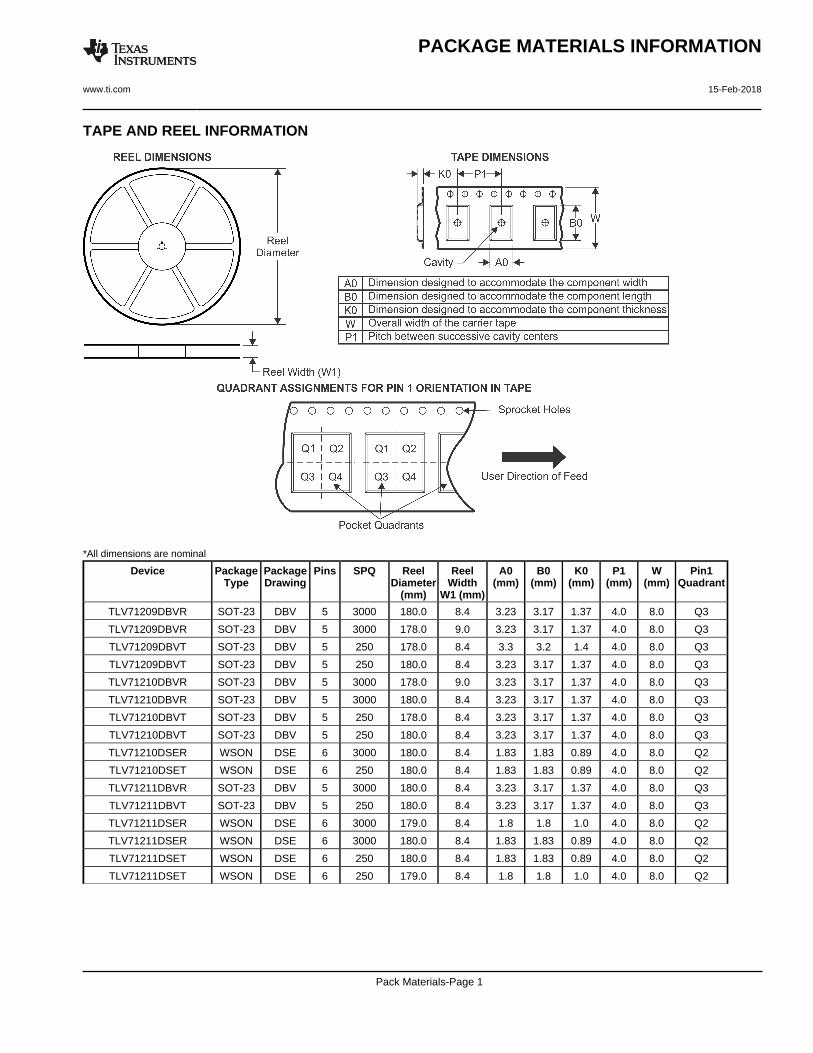
TAPE AND REEL INFORMATION
*All dimensions are nominal
Device PackageType
PackageDrawing
Pins SPQ ReelDiameter
(mm)
ReelWidth
W1 (mm)
A0(mm)
B0(mm)
K0(mm)
P1(mm)
W(mm)
Pin1Quadrant
TLV71209DBVR SOT-23 DBV 5 3000 180.0 8.4 3.23 3.17 1.37 4.0 8.0 Q3
TLV71209DBVR SOT-23 DBV 5 3000 178.0 9.0 3.23 3.17 1.37 4.0 8.0 Q3
TLV71209DBVT SOT-23 DBV 5 250 178.0 8.4 3.3 3.2 1.4 4.0 8.0 Q3
TLV71209DBVT SOT-23 DBV 5 250 180.0 8.4 3.23 3.17 1.37 4.0 8.0 Q3
TLV71210DBVR SOT-23 DBV 5 3000 178.0 9.0 3.23 3.17 1.37 4.0 8.0 Q3
TLV71210DBVR SOT-23 DBV 5 3000 180.0 8.4 3.23 3.17 1.37 4.0 8.0 Q3
TLV71210DBVT SOT-23 DBV 5 250 178.0 8.4 3.23 3.17 1.37 4.0 8.0 Q3
TLV71210DBVT SOT-23 DBV 5 250 180.0 8.4 3.23 3.17 1.37 4.0 8.0 Q3
TLV71210DSER WSON DSE 6 3000 180.0 8.4 1.83 1.83 0.89 4.0 8.0 Q2
TLV71210DSET WSON DSE 6 250 180.0 8.4 1.83 1.83 0.89 4.0 8.0 Q2
TLV71211DBVR SOT-23 DBV 5 3000 180.0 8.4 3.23 3.17 1.37 4.0 8.0 Q3
TLV71211DBVT SOT-23 DBV 5 250 180.0 8.4 3.23 3.17 1.37 4.0 8.0 Q3
TLV71211DSER WSON DSE 6 3000 179.0 8.4 1.8 1.8 1.0 4.0 8.0 Q2
TLV71211DSER WSON DSE 6 3000 180.0 8.4 1.83 1.83 0.89 4.0 8.0 Q2
TLV71211DSET WSON DSE 6 250 180.0 8.4 1.83 1.83 0.89 4.0 8.0 Q2
TLV71211DSET WSON DSE 6 250 179.0 8.4 1.8 1.8 1.0 4.0 8.0 Q2
PACKAGE MATERIALS INFORMATION
www.ti.com 15-Feb-2018
Pack Materials-Page 1
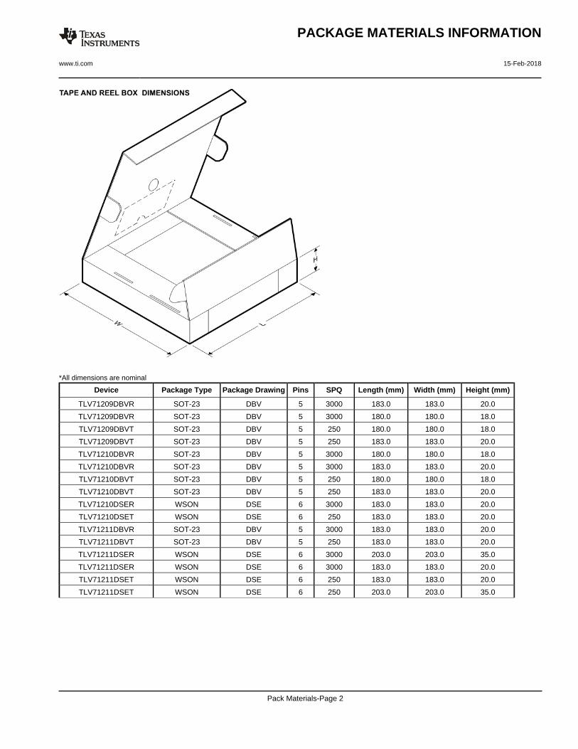
*All dimensions are nominal
Device Package Type Package Drawing Pins SPQ Length (mm) Width (mm) Height (mm)
TLV71209DBVR SOT-23 DBV 5 3000 183.0 183.0 20.0
TLV71209DBVR SOT-23 DBV 5 3000 180.0 180.0 18.0
TLV71209DBVT SOT-23 DBV 5 250 180.0 180.0 18.0
TLV71209DBVT SOT-23 DBV 5 250 183.0 183.0 20.0
TLV71210DBVR SOT-23 DBV 5 3000 180.0 180.0 18.0
TLV71210DBVR SOT-23 DBV 5 3000 183.0 183.0 20.0
TLV71210DBVT SOT-23 DBV 5 250 180.0 180.0 18.0
TLV71210DBVT SOT-23 DBV 5 250 183.0 183.0 20.0
TLV71210DSER WSON DSE 6 3000 183.0 183.0 20.0
TLV71210DSET WSON DSE 6 250 183.0 183.0 20.0
TLV71211DBVR SOT-23 DBV 5 3000 183.0 183.0 20.0
TLV71211DBVT SOT-23 DBV 5 250 183.0 183.0 20.0
TLV71211DSER WSON DSE 6 3000 203.0 203.0 35.0
TLV71211DSER WSON DSE 6 3000 183.0 183.0 20.0
TLV71211DSET WSON DSE 6 250 183.0 183.0 20.0
TLV71211DSET WSON DSE 6 250 203.0 203.0 35.0
PACKAGE MATERIALS INFORMATION
www.ti.com 15-Feb-2018
Pack Materials-Page 2
www.ti.com
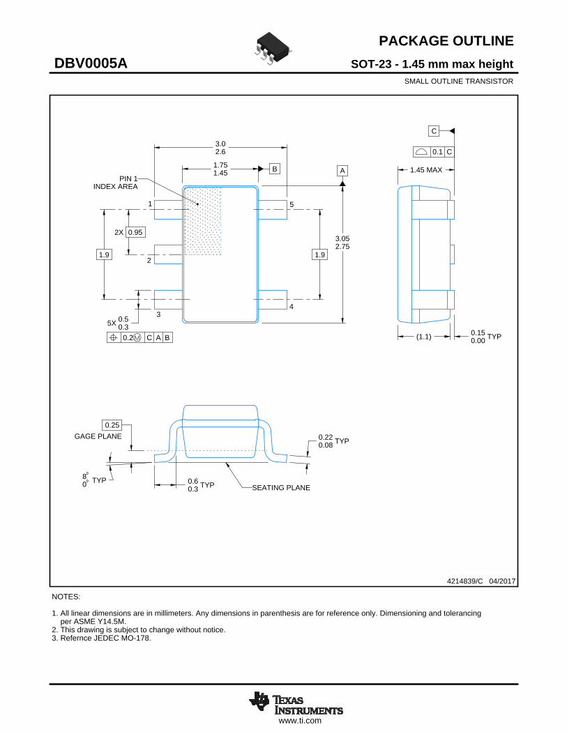
PACKAGE OUTLINE
C
TYP0.220.08
0.25
3.02.6
2X 0.95
1.9
1.45 MAX
TYP0.150.00
5X 0.50.3
TYP0.60.3
TYP80
1.9
A
3.052.75
B1.751.45
(1.1)
SOT-23 - 1.45 mm max heightDBV0005ASMALL OUTLINE TRANSISTOR
4214839/C 04/2017
NOTES: 1. All linear dimensions are in millimeters. Any dimensions in parenthesis are for reference only. Dimensioning and tolerancing per ASME Y14.5M.2. This drawing is subject to change without notice.3. Refernce JEDEC MO-178.
0.2 C A B
1
34
5
2
INDEX AREAPIN 1
GAGE PLANE
SEATING PLANE
0.1 C
SCALE 4.000
www.ti.com
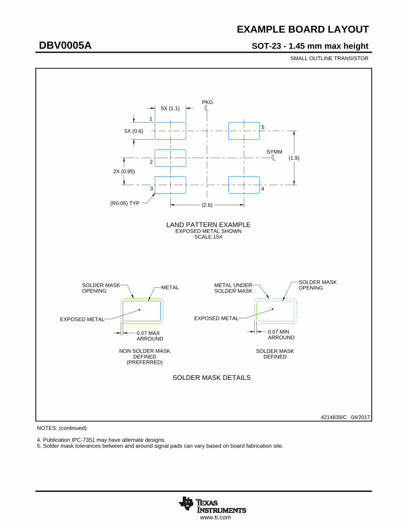
EXAMPLE BOARD LAYOUT
0.07 MAXARROUND
0.07 MINARROUND
5X (1.1)
5X (0.6)
(2.6)
(1.9)
2X (0.95)
(R0.05) TYP
4214839/C 04/2017
SOT-23 - 1.45 mm max heightDBV0005ASMALL OUTLINE TRANSISTOR
NOTES: (continued) 4. Publication IPC-7351 may have alternate designs. 5. Solder mask tolerances between and around signal pads can vary based on board fabrication site.
SYMM
LAND PATTERN EXAMPLEEXPOSED METAL SHOWN
SCALE:15X
PKG
1
3 4
5
2
SOLDER MASKOPENINGMETAL UNDER
SOLDER MASK
SOLDER MASKDEFINED
EXPOSED METAL
METALSOLDER MASKOPENING
NON SOLDER MASKDEFINED
(PREFERRED)
SOLDER MASK DETAILS
EXPOSED METAL
www.ti.com
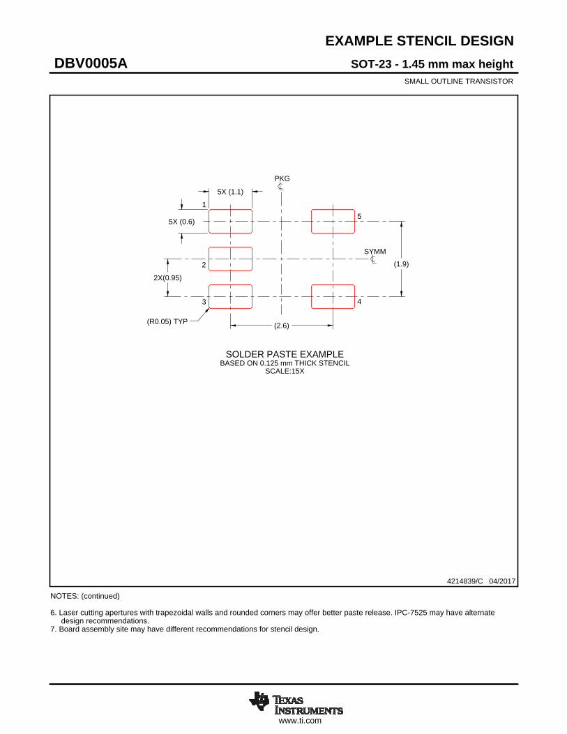
EXAMPLE STENCIL DESIGN
(2.6)
(1.9)
2X(0.95)
5X (1.1)
5X (0.6)
(R0.05) TYP
SOT-23 - 1.45 mm max heightDBV0005ASMALL OUTLINE TRANSISTOR
4214839/C 04/2017
NOTES: (continued) 6. Laser cutting apertures with trapezoidal walls and rounded corners may offer better paste release. IPC-7525 may have alternate design recommendations. 7. Board assembly site may have different recommendations for stencil design.
SOLDER PASTE EXAMPLEBASED ON 0.125 mm THICK STENCIL
SCALE:15X
SYMM
PKG
1
3 4
5
2
IMPORTANT NOTICE
Texas Instruments Incorporated (TI) reserves the right to make corrections, enhancements, improvements and other changes to itssemiconductor products and services per JESD46, latest issue, and to discontinue any product or service per JESD48, latest issue. Buyersshould obtain the latest relevant information before placing orders and should verify that such information is current and complete.TI’s published terms of sale for semiconductor products (http://www.ti.com/sc/docs/stdterms.htm) apply to the sale of packaged integratedcircuit products that TI has qualified and released to market. Additional terms may apply to the use or sale of other types of TI products andservices.Reproduction of significant portions of TI information in TI data sheets is permissible only if reproduction is without alteration and isaccompanied by all associated warranties, conditions, limitations, and notices. TI is not responsible or liable for such reproduceddocumentation. Information of third parties may be subject to additional restrictions. Resale of TI products or services with statementsdifferent from or beyond the parameters stated by TI for that product or service voids all express and any implied warranties for theassociated TI product or service and is an unfair and deceptive business practice. TI is not responsible or liable for any such statements.Buyers and others who are developing systems that incorporate TI products (collectively, “Designers”) understand and agree that Designersremain responsible for using their independent analysis, evaluation and judgment in designing their applications and that Designers havefull and exclusive responsibility to assure the safety of Designers' applications and compliance of their applications (and of all TI productsused in or for Designers’ applications) with all applicable regulations, laws and other applicable requirements. Designer represents that, withrespect to their applications, Designer has all the necessary expertise to create and implement safeguards that (1) anticipate dangerousconsequences of failures, (2) monitor failures and their consequences, and (3) lessen the likelihood of failures that might cause harm andtake appropriate actions. Designer agrees that prior to using or distributing any applications that include TI products, Designer willthoroughly test such applications and the functionality of such TI products as used in such applications.TI’s provision of technical, application or other design advice, quality characterization, reliability data or other services or information,including, but not limited to, reference designs and materials relating to evaluation modules, (collectively, “TI Resources”) are intended toassist designers who are developing applications that incorporate TI products; by downloading, accessing or using TI Resources in anyway, Designer (individually or, if Designer is acting on behalf of a company, Designer’s company) agrees to use any particular TI Resourcesolely for this purpose and subject to the terms of this Notice.TI’s provision of TI Resources does not expand or otherwise alter TI’s applicable published warranties or warranty disclaimers for TIproducts, and no additional obligations or liabilities arise from TI providing such TI Resources. TI reserves the right to make corrections,enhancements, improvements and other changes to its TI Resources. TI has not conducted any testing other than that specificallydescribed in the published documentation for a particular TI Resource.Designer is authorized to use, copy and modify any individual TI Resource only in connection with the development of applications thatinclude the TI product(s) identified in such TI Resource. NO OTHER LICENSE, EXPRESS OR IMPLIED, BY ESTOPPEL OR OTHERWISETO ANY OTHER TI INTELLECTUAL PROPERTY RIGHT, AND NO LICENSE TO ANY TECHNOLOGY OR INTELLECTUAL PROPERTYRIGHT OF TI OR ANY THIRD PARTY IS GRANTED HEREIN, including but not limited to any patent right, copyright, mask work right, orother intellectual property right relating to any combination, machine, or process in which TI products or services are used. Informationregarding or referencing third-party products or services does not constitute a license to use such products or services, or a warranty orendorsement thereof. Use of TI Resources may require a license from a third party under the patents or other intellectual property of thethird party, or a license from TI under the patents or other intellectual property of TI.TI RESOURCES ARE PROVIDED “AS IS” AND WITH ALL FAULTS. TI DISCLAIMS ALL OTHER WARRANTIES ORREPRESENTATIONS, EXPRESS OR IMPLIED, REGARDING RESOURCES OR USE THEREOF, INCLUDING BUT NOT LIMITED TOACCURACY OR COMPLETENESS, TITLE, ANY EPIDEMIC FAILURE WARRANTY AND ANY IMPLIED WARRANTIES OFMERCHANTABILITY, FITNESS FOR A PARTICULAR PURPOSE, AND NON-INFRINGEMENT OF ANY THIRD PARTY INTELLECTUALPROPERTY RIGHTS. TI SHALL NOT BE LIABLE FOR AND SHALL NOT DEFEND OR INDEMNIFY DESIGNER AGAINST ANY CLAIM,INCLUDING BUT NOT LIMITED TO ANY INFRINGEMENT CLAIM THAT RELATES TO OR IS BASED ON ANY COMBINATION OFPRODUCTS EVEN IF DESCRIBED IN TI RESOURCES OR OTHERWISE. IN NO EVENT SHALL TI BE LIABLE FOR ANY ACTUAL,DIRECT, SPECIAL, COLLATERAL, INDIRECT, PUNITIVE, INCIDENTAL, CONSEQUENTIAL OR EXEMPLARY DAMAGES INCONNECTION WITH OR ARISING OUT OF TI RESOURCES OR USE THEREOF, AND REGARDLESS OF WHETHER TI HAS BEENADVISED OF THE POSSIBILITY OF SUCH DAMAGES.Unless TI has explicitly designated an individual product as meeting the requirements of a particular industry standard (e.g., ISO/TS 16949and ISO 26262), TI is not responsible for any failure to meet such industry standard requirements.Where TI specifically promotes products as facilitating functional safety or as compliant with industry functional safety standards, suchproducts are intended to help enable customers to design and create their own applications that meet applicable functional safety standardsand requirements. Using products in an application does not by itself establish any safety features in the application. Designers mustensure compliance with safety-related requirements and standards applicable to their applications. Designer may not use any TI products inlife-critical medical equipment unless authorized officers of the parties have executed a special contract specifically governing such use.Life-critical medical equipment is medical equipment where failure of such equipment would cause serious bodily injury or death (e.g., lifesupport, pacemakers, defibrillators, heart pumps, neurostimulators, and implantables). Such equipment includes, without limitation, allmedical devices identified by the U.S. Food and Drug Administration as Class III devices and equivalent classifications outside the U.S.TI may expressly designate certain products as completing a particular qualification (e.g., Q100, Military Grade, or Enhanced Product).Designers agree that it has the necessary expertise to select the product with the appropriate qualification designation for their applicationsand that proper product selection is at Designers’ own risk. Designers are solely responsible for compliance with all legal and regulatoryrequirements in connection with such selection.Designer will fully indemnify TI and its representatives against any damages, costs, losses, and/or liabilities arising out of Designer’s non-compliance with the terms and provisions of this Notice.
Mailing Address: Texas Instruments, Post Office Box 655303, Dallas, Texas 75265Copyright © 2018, Texas Instruments Incorporated