Embed Size (px)
Citation preview
1
Rev. 0.4
BeRex website: www.berex.com email: [email protected]
Specifications and information are subject to change and products may be discontinued without notice. BeRex is a trademark of BeRex.
All other trademarks are the property of their respective owners. © 2017 BeRex
Pre
limin
ary
Dat
ash
eet
1
7 12
18
13
24 19
C1 2
3
4
5
6
C0.5
GND
AMPOUT
GND
C16
8 9 10 11
14
15
16
17
20212223
GND
GND
PUP2
PUP1
LE
VDD
GN
D
AM
PIN
GN
D
RF
1
Da
ta
Clo
ck
C2
C4
C8
RF
2
P/S
VS
S/G
ND
Digital Step Attenuation
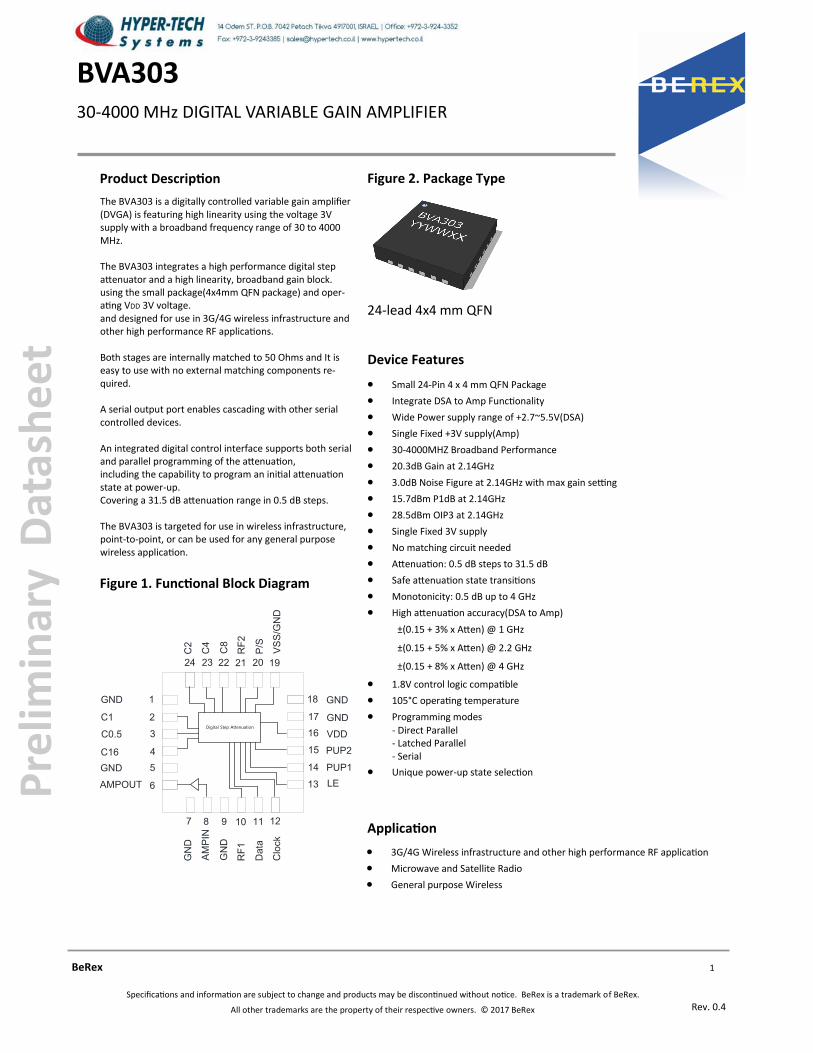
30-4000 MHz DIGITAL VARIABLE GAIN AMPLIFIER
BVA303
Figure 1. Functional Block Diagram
Device Features
Figure 2. Package Type
24-lead 4x4 mm QFN
Small 24-Pin 4 x 4 mm QFN Package
Integrate DSA to Amp Functionality
Wide Power supply range of +2.7~5.5V(DSA)
Single Fixed +3V supply(Amp)
30-4000MHZ Broadband Performance
20.3dB Gain at 2.14GHz
3.0dB Noise Figure at 2.14GHz with max gain setting
15.7dBm P1dB at 2.14GHz
28.5dBm OIP3 at 2.14GHz
Single Fixed 3V supply
No matching circuit needed
Attenuation: 0.5 dB steps to 31.5 dB
Safe attenuation state transitions
Monotonicity: 0.5 dB up to 4 GHz
High attenuation accuracy(DSA to Amp)
±(0.15 + 3% x Atten) @ 1 GHz
±(0.15 + 5% x Atten) @ 2.2 GHz
±(0.15 + 8% x Atten) @ 4 GHz
1.8V control logic compatible
105°C operating temperature
Programming modes
- Direct Parallel - Latched Parallel - Serial
Unique power-up state selection
Application
3G/4G Wireless infrastructure and other high performance RF application
Microwave and Satellite Radio
General purpose Wireless
Product Description
The BVA303 is a digitally controlled variable gain amplifier (DVGA) is featuring high linearity using the voltage 3V supply with a broadband frequency range of 30 to 4000 MHz. The BVA303 integrates a high performance digital step attenuator and a high linearity, broadband gain block. using the small package(4x4mm QFN package) and oper-ating VDD 3V voltage. and designed for use in 3G/4G wireless infrastructure and other high performance RF applications. Both stages are internally matched to 50 Ohms and It is easy to use with no external matching components re-quired. A serial output port enables cascading with other serial controlled devices. An integrated digital control interface supports both serial and parallel programming of the attenuation, including the capability to program an initial attenuation state at power-up. Covering a 31.5 dB attenuation range in 0.5 dB steps. The BVA303 is targeted for use in wireless infrastructure, point-to-point, or can be used for any general purpose wireless application.
2
Rev. 0.4
BeRex website: www.berex.com email: [email protected]
Specifications and information are subject to change and products may be discontinued without notice. BeRex is a trademark of BeRex.
All other trademarks are the property of their respective owners. © 2017 BeRex
Pre
limin
ary
Dat
ash
eet
30-4000 MHz DIGITAL VARIABLE GAIN AMPLIFIER
BVA303
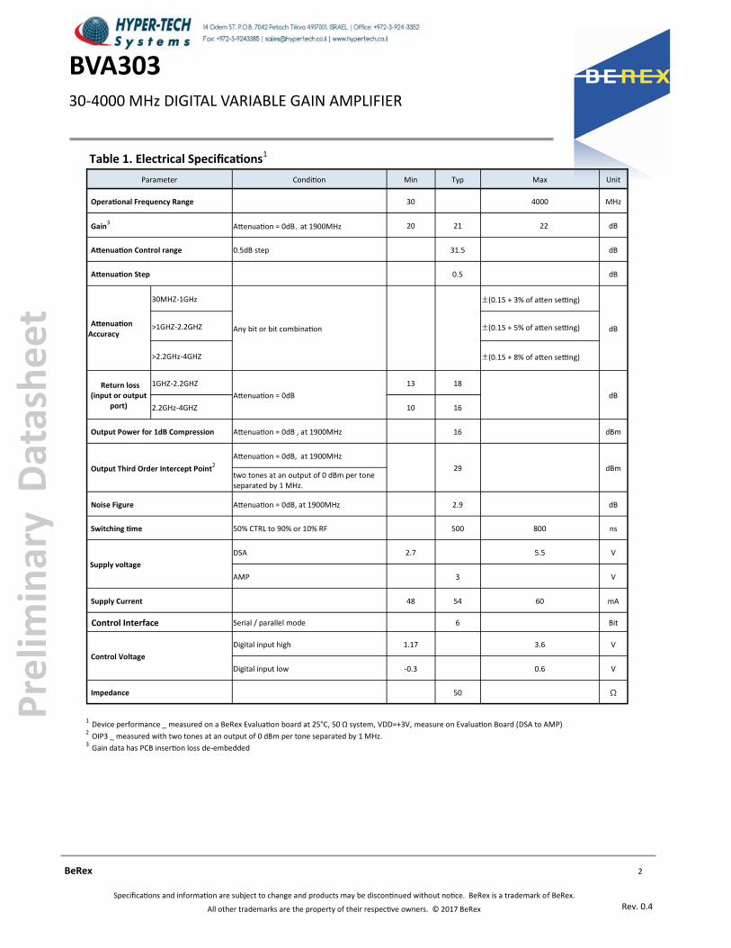
Parameter Condition Min Typ Max Unit
Operational Frequency Range 30 4000 MHz
Gain3 Attenuation = 0dB, at 1900MHz 20 21 22 dB
Attenuation Control range 0.5dB step 31.5 dB
Attenuation Step 0.5 dB
Attenuation Accuracy
30MHZ-1GHz
Any bit or bit combination
±(0.15 + 3% of atten setting)
dB >1GHZ-2.2GHZ ±(0.15 + 5% of atten setting)
>2.2GHz-4GHZ ±(0.15 + 8% of atten setting)
Return loss (input or output
port)
1GHZ-2.2GHZ
Attenuation = 0dB
13 18
dB
2.2GHz-4GHZ 10 16
Output Power for 1dB Compression Attenuation = 0dB , at 1900MHz 16 dBm
Output Third Order Intercept Point2
Attenuation = 0dB, at 1900MHz
29 dBm two tones at an output of 0 dBm per tone separated by 1 MHz.
Noise Figure Attenuation = 0dB, at 1900MHz 2.9 dB
Switching time 50% CTRL to 90% or 10% RF 500 800 ns
Supply voltage
DSA 2.7 5.5 V
AMP 3 V
Supply Current 48 54 60 mA
Control Interface Serial / parallel mode 6 Bit
Control Voltage
Digital input high 1.17 3.6 V
Digital input low -0.3 0.6 V
Impedance 50 Ω
1 Device performance _ measured on a BeRex Evaluation board at 25°C, 50 Ω system, VDD=+3V, measure on Evaluation Board (DSA to AMP)
2 OIP3 _ measured with two tones at an output of 0 dBm per tone separated by 1 MHz.
3 Gain data has PCB insertion loss de-embedded
Table 1. Electrical Specifications1
3
Rev. 0.4
BeRex website: www.berex.com email: [email protected]
Specifications and information are subject to change and products may be discontinued without notice. BeRex is a trademark of BeRex.
All other trademarks are the property of their respective owners. © 2017 BeRex
Pre
limin
ary
Dat
ash
eet
30-4000 MHz DIGITAL VARIABLE GAIN AMPLIFIER
BVA303
1 Device performance _ measured on a BeRex evaluation board at 25°C, VDD=+3V,50 Ω system. measure on Evaluation Board (DSA to AMP)
2 OIP3 _ measured with two tones at an output of 0 dBm per tone separated by 1 MHz.
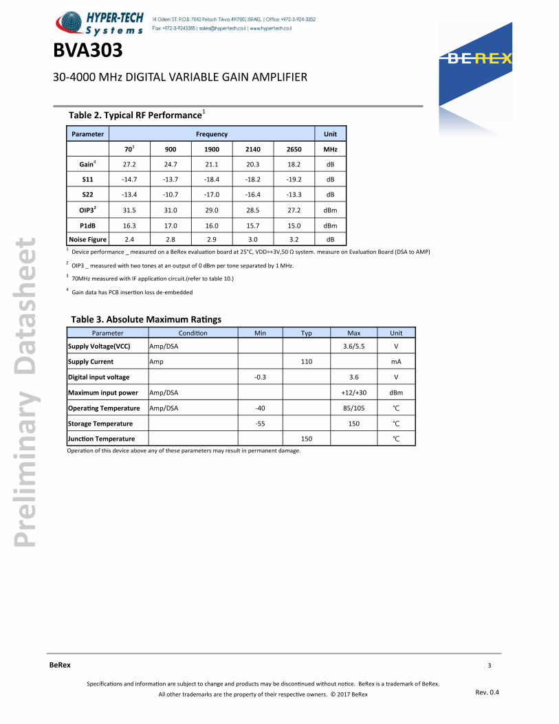
Table 2. Typical RF Performance1
Table 3. Absolute Maximum Ratings
Operation of this device above any of these parameters may result in permanent damage.
Parameter Frequency Unit
703 900 1900 2140 2650 MHz
Gain4 27.2 24.7 21.1 20.3 18.2 dB
S11 -14.7 -13.7 -18.4 -18.2 -19.2 dB
S22 -13.4 -10.7 -17.0 -16.4 -13.3 dB
OIP32 31.5 31.0 29.0 28.5 27.2 dBm
P1dB 16.3 17.0 16.0 15.7 15.0 dBm
Noise Figure 2.4 2.8 2.9 3.0 3.2 dB
3 70MHz measured with IF application circuit.(refer to table 10.)
Parameter Condition Min Typ Max Unit
Supply Voltage(VCC) Amp/DSA 3.6/5.5 V
Supply Current Amp 110 mA
Digital input voltage -0.3 3.6 V
Maximum input power Amp/DSA +12/+30 dBm
Operating Temperature Amp/DSA -40 85/105
Storage Temperature -55 150
Junction Temperature 150
4 Gain data has PCB insertion loss de-embedded
4
Rev. 0.4
BeRex website: www.berex.com email: [email protected]
Specifications and information are subject to change and products may be discontinued without notice. BeRex is a trademark of BeRex.
All other trademarks are the property of their respective owners. © 2017 BeRex
Pre
limin
ary
Dat
ash
eet
30-4000 MHz DIGITAL VARIABLE GAIN AMPLIFIER
BVA303
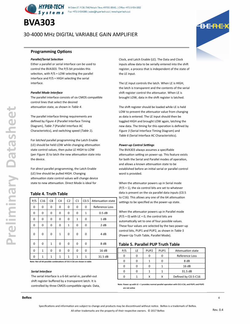
Programming Options
Parallel/Serial Selection
Either a parallel or serial interface can be used to
control the BVA303. The P/S bit provides this
selection, with P/S = LOW selecting the parallel
interface and P/S = HIGH selecting the serial
interface.
Parallel Mode Interface
The parallel interface consists of six CMOS compatible
control lines that select the desired
attenuation state, as shown in Table 4.
The parallel interface timing requirements are
defined by Figure 4 (Parallel Interface Timing
Diagram), Table 7 (Parallel Interface AC
Characteristics), and switching speed (Table 1).
For latched parallel programming the Latch Enable
(LE) should be held LOW while changing attenuation
state control values, then pulse LE HIGH to LOW
(per Figure 3) to latch the new attenuation state into
the device.
For direct parallel programming, the Latch Enable
(LE) line should be pulled HIGH. Changing
attenuation state control values will change device
state to new attenuation. Direct Mode is ideal for
P/S C16 C8 C4 C2 C1 C0.5 Attenuation state
0 0 0 0 0 0 0 Reference Loss
0 0 0 0 0 0 1 0.5 dB
0 0 0 0 0 1 0 1 dB
0 0 0 0 1 0 0 2 dB
0 0 0 1 0 0 0 4 dB
0 0 1 0 0 0 0 8 dB
0 1 0 0 0 0 0 16 dB
0 1 1 1 1 1 1 31.5 dB
Table 4. Truth Table
Clock, and Latch Enable (LE). The Data and Clock
inputs allow data to be serially entered into the shift
register, a process that is independent of the state of
the LE input.
The LE input controls the latch. When LE is HIGH,
the latch is transparent and the contents of the serial
shift register control the attenuator. When LE is
brought LOW, data in the shift register is latched.
The shift register should be loaded while LE is held
LOW to prevent the attenuator value from changing
as data is entered. The LE input should then be
toggled HIGH and brought LOW again, latching the
new data. The timing for this operation is defined by
Figure 3 (Serial Interface Timing Diagram) and
Table 6 (Serial Interface AC Characteristics).
Power-up Control Settings
The BVA303 always assumes a specifiable
attenuation setting on power-up. This feature exists
for both the Serial and Parallel modes of operation,
and allows a known attenuation state to be
established before an initial serial or parallel control
word is provided.
When the attenuator powers up in Serial mode
(P/S = 1), the six control bits are set to whatever
data is present on the six parallel data inputs (C0.5
to C16). This allows any one of the 64 attenuation
settings to be specified as the power-up state.
When the attenuator powers up in Parallel mode
(P/S = 0) with LE = 0, the control bits are
automatically set to one of four possible values.
These four values are selected by the two power-up
control bits, PUP1 and PUP2, as shown in Table 5
(Power-Up Truth Table, Parallel Mode).
Serial Interface
The serial interface is a 6-bit serial-in, parallel-out
shift register buffered by a transparent latch. It is
controlled by three CMOS-compatible signals: Data,
P/S LE PUP2 PUP1 Attenuation state
0 0 0 0 Reference Loss
0 0 1 0 8 dB
0 0 0 1 16 dB
0 0 1 1 31.5 dB
0 1 X X Defined by C0.5-C16
Table 5. Parallel PUP Truth Table
Note: Not all 64 possible combinations of C0.5-C16 are shown in table
Note: Power up with LE = 1 provides normal parallel operation with C0.5-C16, and PUP1 and PUP2
are not active
5
Rev. 0.4
BeRex website: www.berex.com email: [email protected]
Specifications and information are subject to change and products may be discontinued without notice. BeRex is a trademark of BeRex.
All other trademarks are the property of their respective owners. © 2017 BeRex
Pre
limin
ary
Dat
ash
eet
1
7 12
18
13
24 19
C1 2
3
4
5
6
C0.5
GND
AMPOUT
GND
C16
8 9 10 11
14
15
16
17
20212223
GND
GND
PUP2
PUP1
LE
VDD
GN
D
AM
PIN
GN
D
RF
1
Da
ta
Clo
ck
C2
C4
C8
RF
2
P/S
VS
S/G
ND
EXPOSED
Grounnd Pad
30-4000 MHz DIGITAL VARIABLE GAIN AMPLIFIER
BVA303
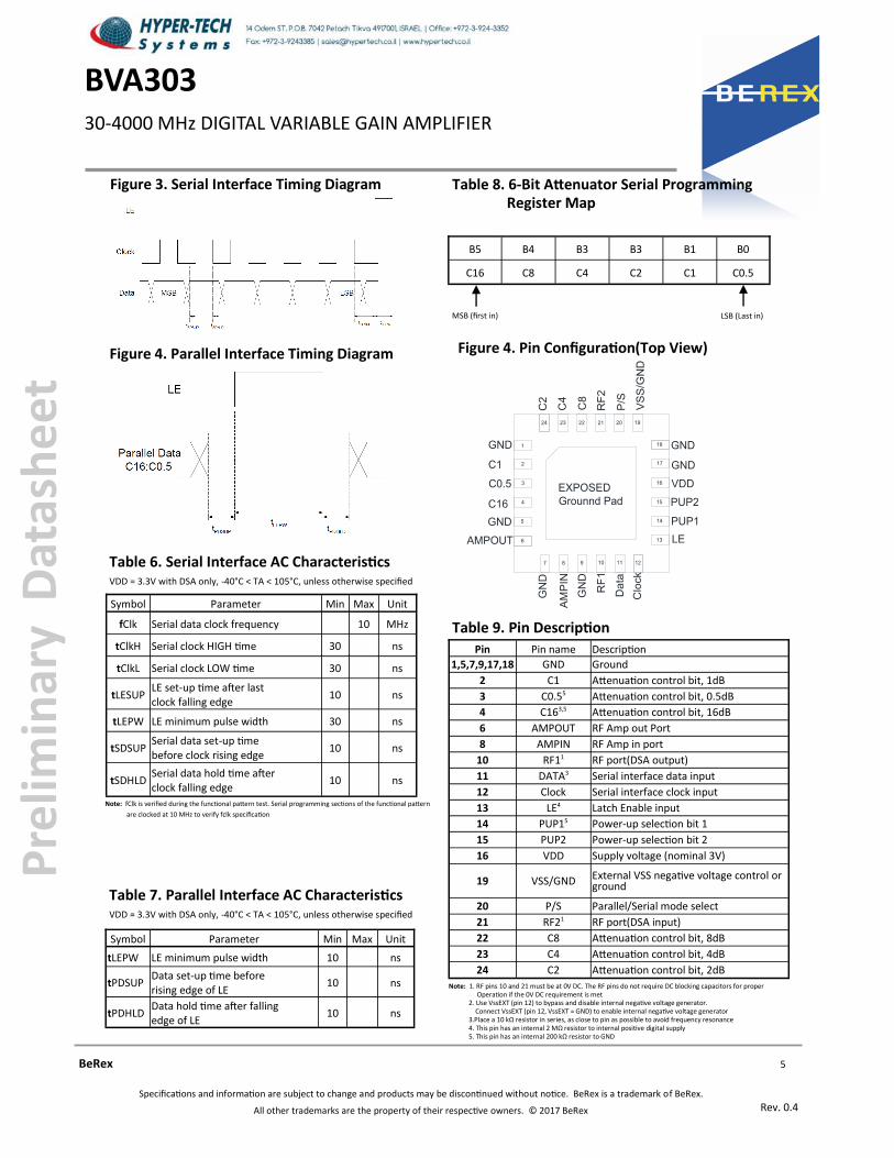
Note: 1. RF pins 10 and 21 must be at 0V DC. The RF pins do not require DC blocking capacitors for proper Operation if the 0V DC requirement is met 2. Use VssEXT (pin 12) to bypass and disable internal negative voltage generator. Connect VssEXT (pin 12, VssEXT = GND) to enable internal negative voltage generator 3.Place a 10 kΩ resistor in series, as close to pin as possible to avoid frequency resonance 4. This pin has an internal 2 MΩ resistor to internal positive digital supply 5. This pin has an internal 200 kΩ resistor to GND
Figure 3. Serial Interface Timing Diagram
Figure 4. Parallel Interface Timing Diagram
Pin Pin name Description
1,5,7,9,17,18 GND Ground
2 C1 Attenuation control bit, 1dB
3 C0.55 Attenuation control bit, 0.5dB
4 C163,5 Attenuation control bit, 16dB
6 AMPOUT RF Amp out Port
8 AMPIN RF Amp in port
10 RF11 RF port(DSA output)
11 DATA3 Serial interface data input
12 Clock Serial interface clock input
13 LE4 Latch Enable input
14 PUP15 Power-up selection bit 1
15 PUP2 Power-up selection bit 2
16 VDD Supply voltage (nominal 3V)
19 VSS/GND External VSS negative voltage control or ground
20 P/S Parallel/Serial mode select
21 RF21 RF port(DSA input)
22 C8 Attenuation control bit, 8dB
23 C4 Attenuation control bit, 4dB
24 C2 Attenuation control bit, 2dB
Table 9. Pin Description
Table 6. Serial Interface AC Characteristics VDD = 3.3V with DSA only, -40°C < TA < 105°C, unless otherwise specified
Symbol Parameter Min Max Unit
fClk Serial data clock frequency 10 MHz
tClkH Serial clock HIGH time 30 ns
tClkL Serial clock LOW time 30 ns
tLESUP LE set-up time after last clock falling edge
10 ns
tLEPW LE minimum pulse width 30 ns
tSDSUP Serial data set-up time before clock rising edge
10 ns
tSDHLD Serial data hold time after clock falling edge
10 ns
Table 8. 6-Bit Attenuator Serial Programming Register Map
B5 B4 B3 B3 B1 B0
C16 C8 C4 C2 C1 C0.5
MSB (first in) LSB (Last in)
Table 7. Parallel Interface AC Characteristics VDD = 3.3V with DSA only, -40°C < TA < 105°C, unless otherwise specified
Symbol Parameter Min Max Unit
tLEPW LE minimum pulse width 10 ns
tPDSUP Data set-up time before rising edge of LE
10 ns
tPDHLD Data hold time after falling edge of LE
10 ns
Figure 4. Pin Configuration(Top View)
Note: fClk is verified during the functional pattern test. Serial programming sections of the functional pattern
are clocked at 10 MHz to verify fclk specification
6
Rev. 0.4
BeRex website: www.berex.com email: [email protected]
Specifications and information are subject to change and products may be discontinued without notice. BeRex is a trademark of BeRex.
All other trademarks are the property of their respective owners. © 2017 BeRex
Pre
limin
ary
Dat
ash
eet
30-4000 MHz DIGITAL VARIABLE GAIN AMPLIFIER
BVA303
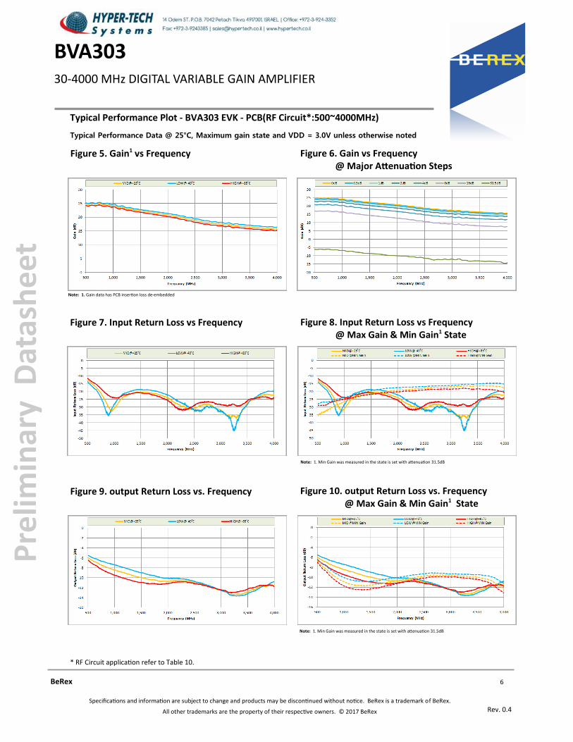
Figure 6. Gain vs Frequency @ Major Attenuation Steps
Typical Performance Data @ 25°C, Maximum gain state and VDD = 3.0V unless otherwise noted
Figure 5. Gain1 vs Frequency
Typical Performance Plot - BVA303 EVK - PCB(RF Circuit*:500~4000MHz)
Figure 7. Input Return Loss vs Frequency
Figure 8. Input Return Loss vs Frequency @ Max Gain & Min Gain1 State
Figure 9. output Return Loss vs. Frequency Figure 10. output Return Loss vs. Frequency @ Max Gain & Min Gain1 State
* RF Circuit application refer to Table 10.
Note: 1. Min Gain was measured in the state is set with attenuation 31.5dB
Note: 1. Min Gain was measured in the state is set with attenuation 31.5dB
Note: 1. Gain data has PCB insertion loss de-embedded
7
Rev. 0.4
BeRex website: www.berex.com email: [email protected]
Specifications and information are subject to change and products may be discontinued without notice. BeRex is a trademark of BeRex.
All other trademarks are the property of their respective owners. © 2017 BeRex
Pre
limin
ary
Dat
ash
eet
30-4000 MHz DIGITAL VARIABLE GAIN AMPLIFIER
BVA303
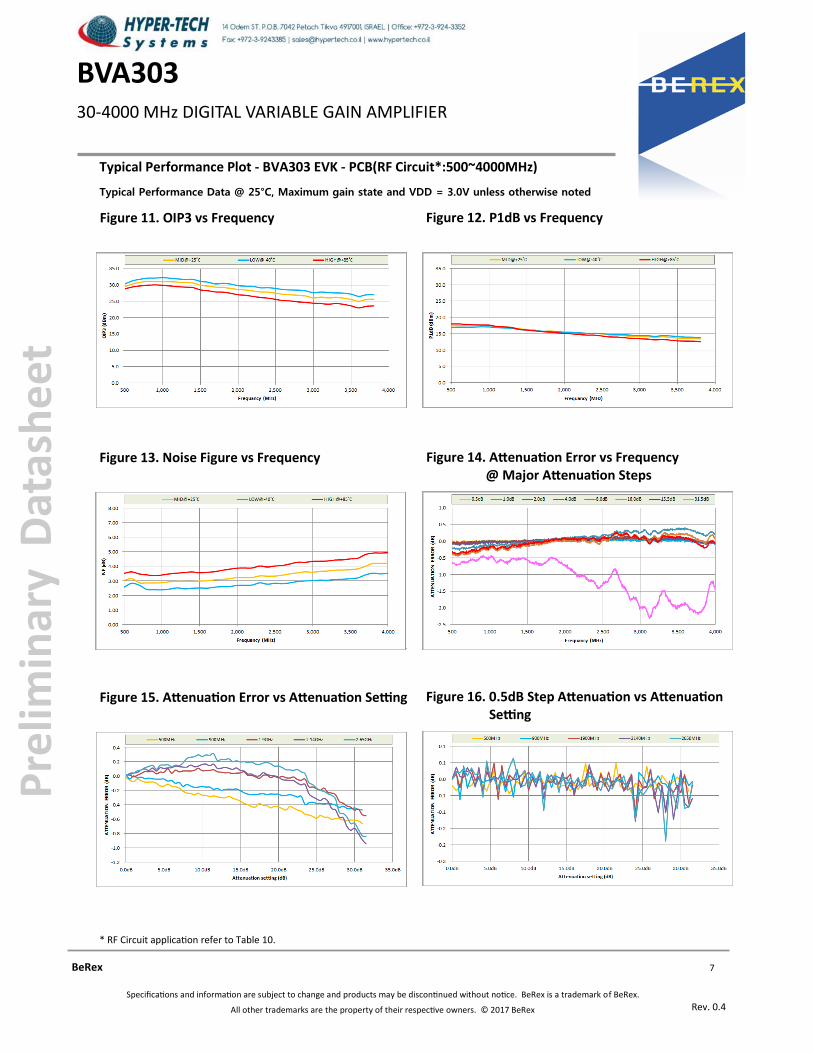
Figure 12. P1dB vs Frequency
Typical Performance Data @ 25°C, Maximum gain state and VDD = 3.0V unless otherwise noted
Figure 11. OIP3 vs Frequency
Typical Performance Plot - BVA303 EVK - PCB(RF Circuit*:500~4000MHz)
Figure 13. Noise Figure vs Frequency
Figure 14. Attenuation Error vs Frequency @ Major Attenuation Steps
Figure 15. Attenuation Error vs Attenuation Setting
Figure 16. 0.5dB Step Attenuation vs Attenuation Setting
* RF Circuit application refer to Table 10.
8
Rev. 0.4
BeRex website: www.berex.com email: [email protected]
Specifications and information are subject to change and products may be discontinued without notice. BeRex is a trademark of BeRex.
All other trademarks are the property of their respective owners. © 2017 BeRex
Pre
limin
ary
Dat
ash
eet
30-4000 MHz DIGITAL VARIABLE GAIN AMPLIFIER
BVA303
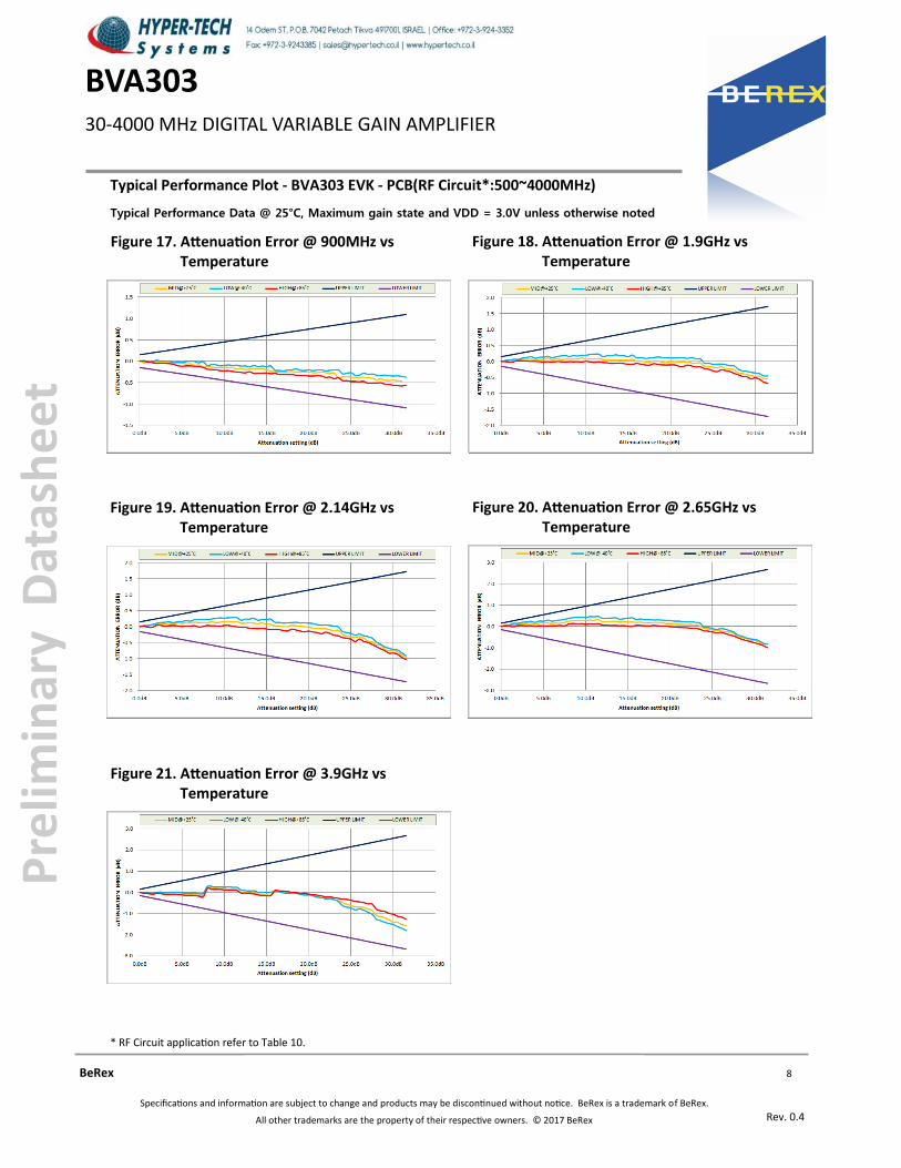
Figure 18. Attenuation Error @ 1.9GHz vs Temperature
Typical Performance Data @ 25°C, Maximum gain state and VDD = 3.0V unless otherwise noted
Figure 17. Attenuation Error @ 900MHz vs Temperature
Typical Performance Plot - BVA303 EVK - PCB(RF Circuit*:500~4000MHz)
Figure 19. Attenuation Error @ 2.14GHz vs Temperature
Figure 20. Attenuation Error @ 2.65GHz vs Temperature
Figure 21. Attenuation Error @ 3.9GHz vs Temperature
* RF Circuit application refer to Table 10.
9
Rev. 0.4
BeRex website: www.berex.com email: [email protected]
Specifications and information are subject to change and products may be discontinued without notice. BeRex is a trademark of BeRex.
All other trademarks are the property of their respective owners. © 2017 BeRex
Pre
limin
ary
Dat
ash
eet
30-4000 MHz DIGITAL VARIABLE GAIN AMPLIFIER
BVA303
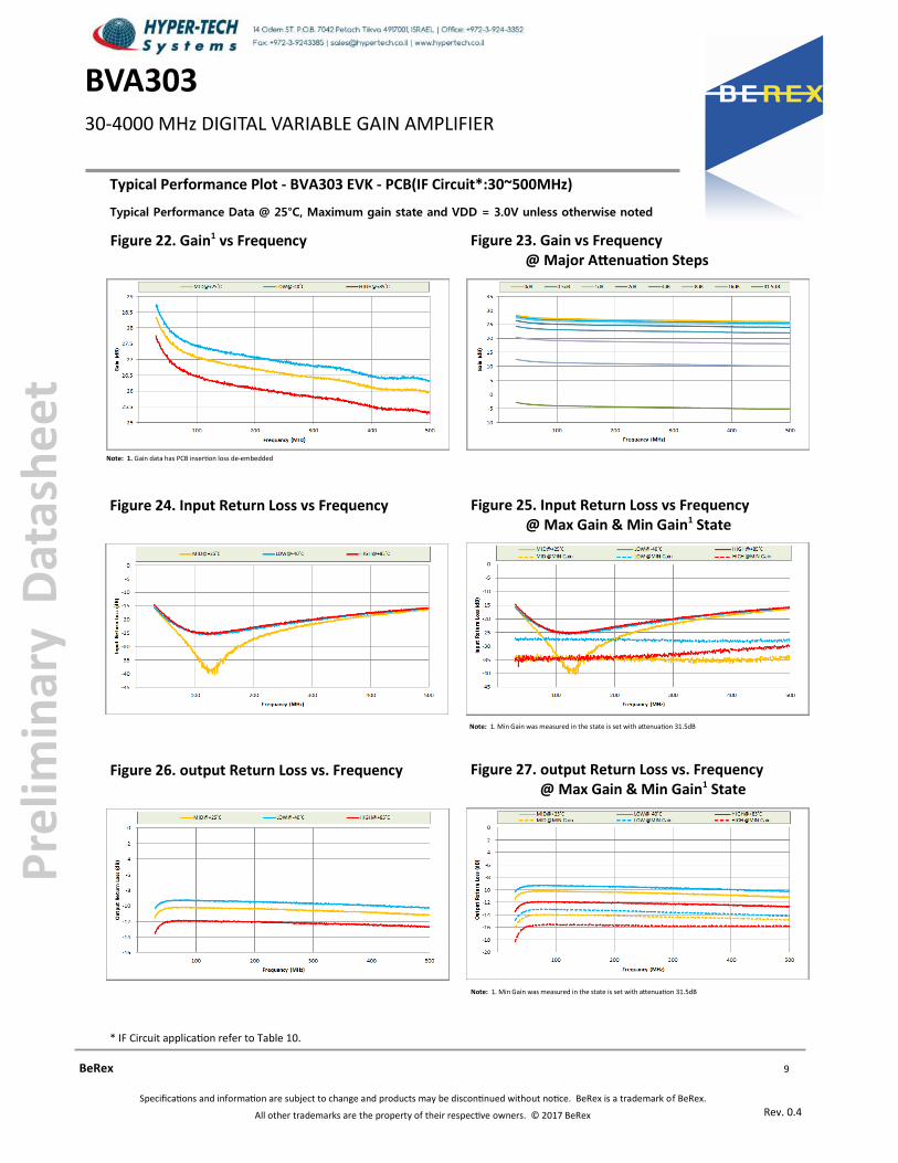
Figure 23. Gain vs Frequency @ Major Attenuation Steps
Typical Performance Data @ 25°C, Maximum gain state and VDD = 3.0V unless otherwise noted
Figure 22. Gain1 vs Frequency
Typical Performance Plot - BVA303 EVK - PCB(IF Circuit*:30~500MHz)
Figure 24. Input Return Loss vs Frequency
Figure 25. Input Return Loss vs Frequency @ Max Gain & Min Gain1 State
Figure 26. output Return Loss vs. Frequency Figure 27. output Return Loss vs. Frequency @ Max Gain & Min Gain1 State
* IF Circuit application refer to Table 10.
Note: 1. Min Gain was measured in the state is set with attenuation 31.5dB
Note: 1. Min Gain was measured in the state is set with attenuation 31.5dB
Note: 1. Gain data has PCB insertion loss de-embedded
10
Rev. 0.4
BeRex website: www.berex.com email: [email protected]
Specifications and information are subject to change and products may be discontinued without notice. BeRex is a trademark of BeRex.
All other trademarks are the property of their respective owners. © 2017 BeRex
Pre
limin
ary
Dat
ash
eet
30-4000 MHz DIGITAL VARIABLE GAIN AMPLIFIER
BVA303
Figure 29. P1dB vs Frequency
Typical Performance Data @ 25°C, Maximum gain state and VDD = 3.0V unless otherwise noted
Figure 28. OIP3 vs Frequency
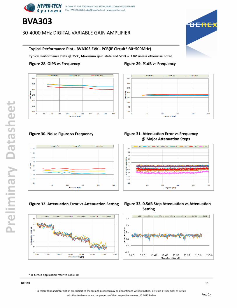
Typical Performance Plot - BVA303 EVK - PCB(IF Circuit*:30~500MHz)
Figure 30. Noise Figure vs Frequency
Figure 31. Attenuation Error vs Frequency @ Major Attenuation Steps
Figure 32. Attenuation Error vs Attenuation Setting
Figure 33. 0.5dB Step Attenuation vs Attenuation Setting
* IF Circuit application refer to Table 10.
11
Rev. 0.4
BeRex website: www.berex.com email: [email protected]
Specifications and information are subject to change and products may be discontinued without notice. BeRex is a trademark of BeRex.
All other trademarks are the property of their respective owners. © 2017 BeRex
Pre
limin
ary
Dat
ash
eet
30-4000 MHz DIGITAL VARIABLE GAIN AMPLIFIER
BVA303
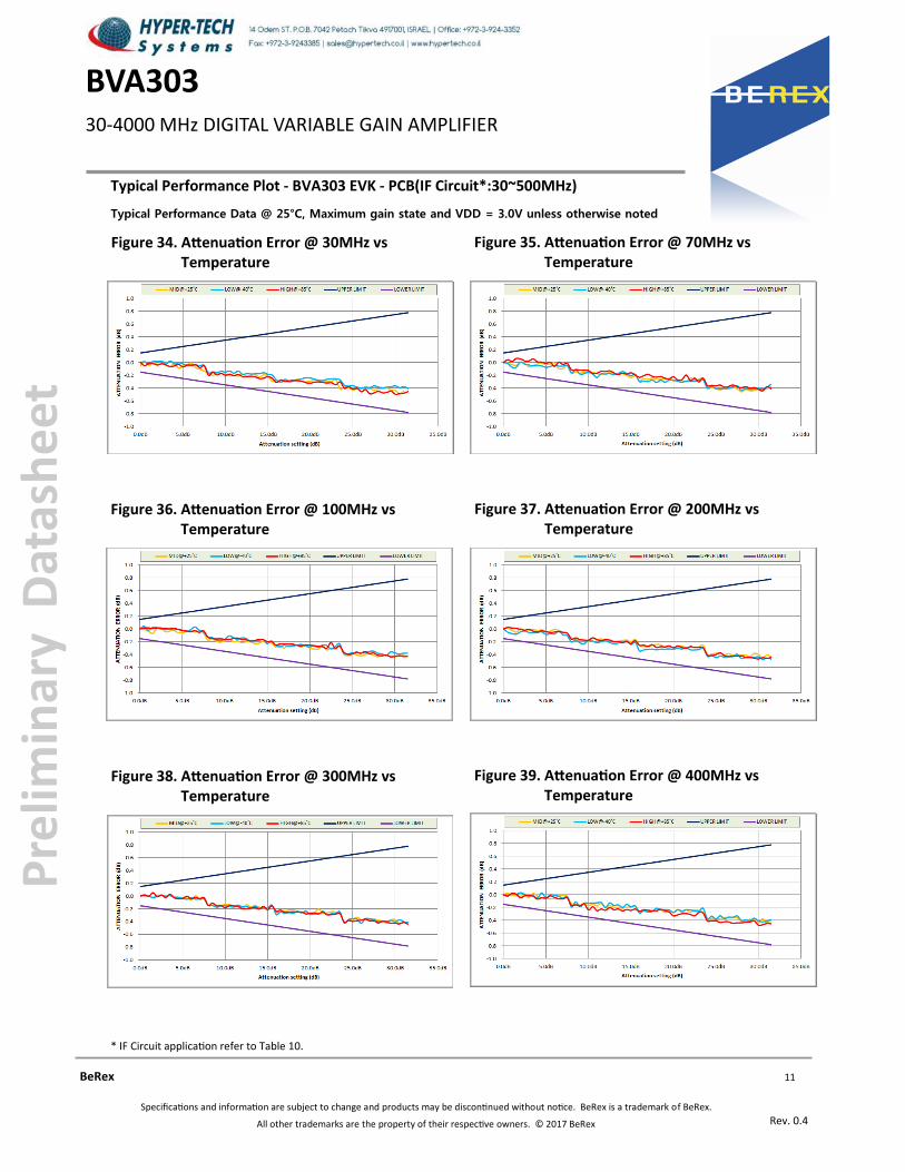
Figure 35. Attenuation Error @ 70MHz vs Temperature
Typical Performance Data @ 25°C, Maximum gain state and VDD = 3.0V unless otherwise noted
Figure 34. Attenuation Error @ 30MHz vs Temperature
Typical Performance Plot - BVA303 EVK - PCB(IF Circuit*:30~500MHz)
Figure 36. Attenuation Error @ 100MHz vs Temperature
Figure 37. Attenuation Error @ 200MHz vs Temperature
Figure 38. Attenuation Error @ 300MHz vs Temperature
Figure 39. Attenuation Error @ 400MHz vs Temperature
* IF Circuit application refer to Table 10.
12
Rev. 0.4
BeRex website: www.berex.com email: [email protected]
Specifications and information are subject to change and products may be discontinued without notice. BeRex is a trademark of BeRex.
All other trademarks are the property of their respective owners. © 2017 BeRex
Pre
limin
ary
Dat
ash
eet
30-4000 MHz DIGITAL VARIABLE GAIN AMPLIFIER
BVA303
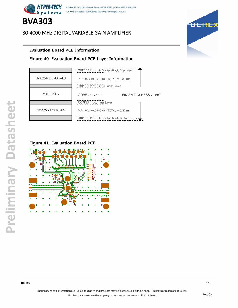
Evaluation Board PCB Information
Figure 40. Evaluation Board PCB Layer Information
Figure 41. Evaluation Board PCB
COPPER :1oz + 0.5oz (plating), Top Layer
COPPER :1oz (GND), Inner Layer
COPPER :1oz + 0.5oz (plating), Bottom Layer
P.P : (0.2+0.06+0.06) TOTAL = 0.32mm
CORE : 0.73mm FINISH TICKNESS :1.55T
P.P : (0.2+0.06+0.06) TOTAL = 0.32mm
COPPER :1oz, Inner Layer
EM825B ER: 4.6~4.8
MTC Er:4.6
EM825B Er:4.6~4.8
13
Rev. 0.4
BeRex website: www.berex.com email: [email protected]
Specifications and information are subject to change and products may be discontinued without notice. BeRex is a trademark of BeRex.
All other trademarks are the property of their respective owners. © 2017 BeRex
Pre
limin
ary
Dat
ash
eet
30-4000 MHz DIGITAL VARIABLE GAIN AMPLIFIER
BVA303
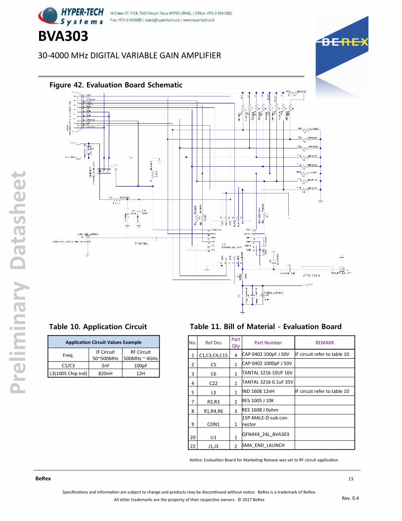
Figure 42. Evaluation Board Schematic
Application Circuit Values Example
Freq. IF Circuit
50~500MHz RF Circuit
500MHz ~ 4GHz
C1/C3 2nF 100pF
L3(1005 Chip Ind) 820nH 12H
Table 10. Application Circuit Table 11. Bill of Material - Evaluation Board
No. Ref Des Part Qty
Part Number REMARK
1 C1,C3,C4,C15 4 CAP 0402 100pF J 50V IF circuit refer to table 10
2 C5 1 CAP 0402 1000pF J 50V
3 C6 1 TANTAL 3216 10UF 16V
4 C22 1 TANTAL 3216 0.1uF 35V
5 L3 1 IND 1608 12nH IF circuit refer to table 10
7 R2,R3 2 RES 1005 J 10K
8 R1,R4,R6 3 RES 1608 J 0ohm
9 CON1 1 15P-MALE-D-sub con-nector
20 U1 1 QFN4X4_24L_BVA303
22 J1,J3 2 SMA_END_LAUNCH
Notice: Evaluation Board for Marketing Release was set to RF circuit application
14
Rev. 0.4
BeRex website: www.berex.com email: [email protected]
Specifications and information are subject to change and products may be discontinued without notice. BeRex is a trademark of BeRex.
All other trademarks are the property of their respective owners. © 2017 BeRex
Pre
limin
ary
Dat
ash
eet
30-4000 MHz DIGITAL VARIABLE GAIN AMPLIFIER
BVA303
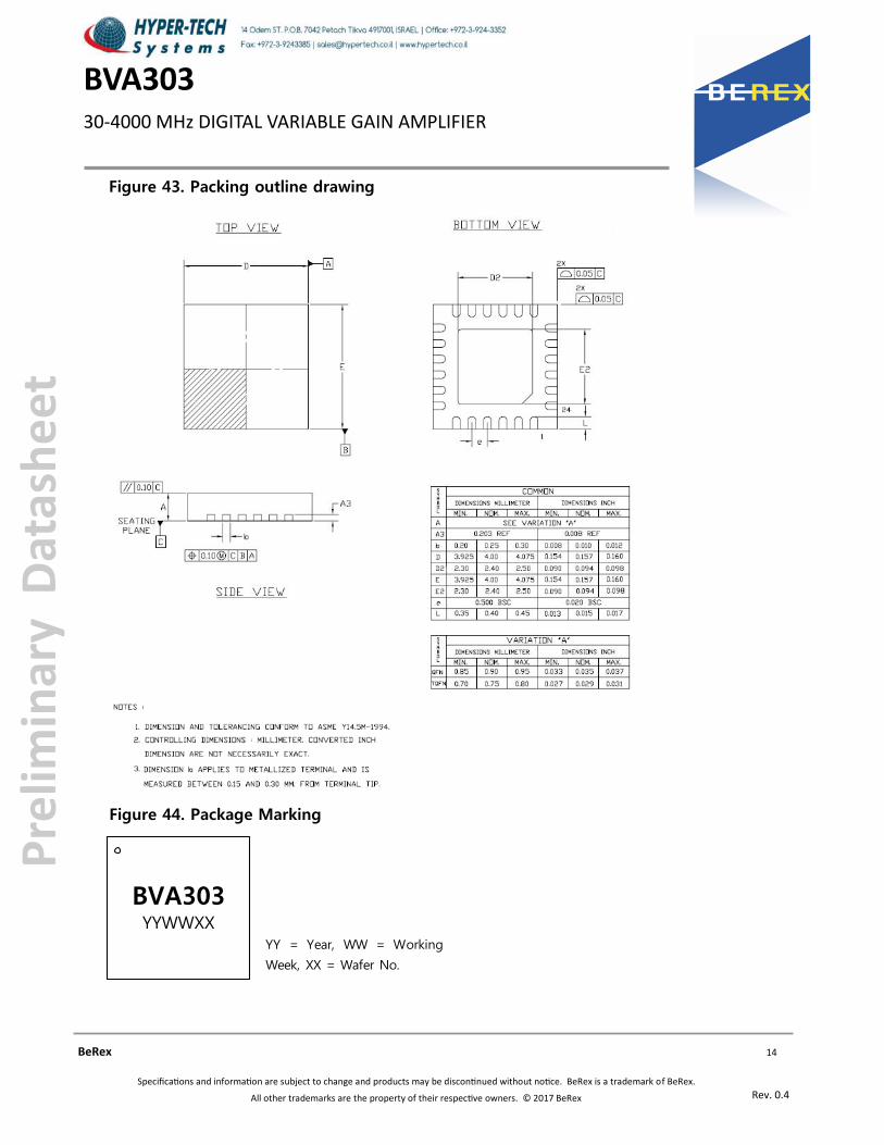
Figure 43. Packing outline drawing
YY = Year, WW = Working
Week, XX = Wafer No.
Figure 44. Package Marking
BVA303YYWWXX
15
Rev. 0.4
BeRex website: www.berex.com email: [email protected]
Specifications and information are subject to change and products may be discontinued without notice. BeRex is a trademark of BeRex.
All other trademarks are the property of their respective owners. © 2017 BeRex
Pre
limin
ary
Dat
ash
eet
30-4000 MHz DIGITAL VARIABLE GAIN AMPLIFIER
BVA303
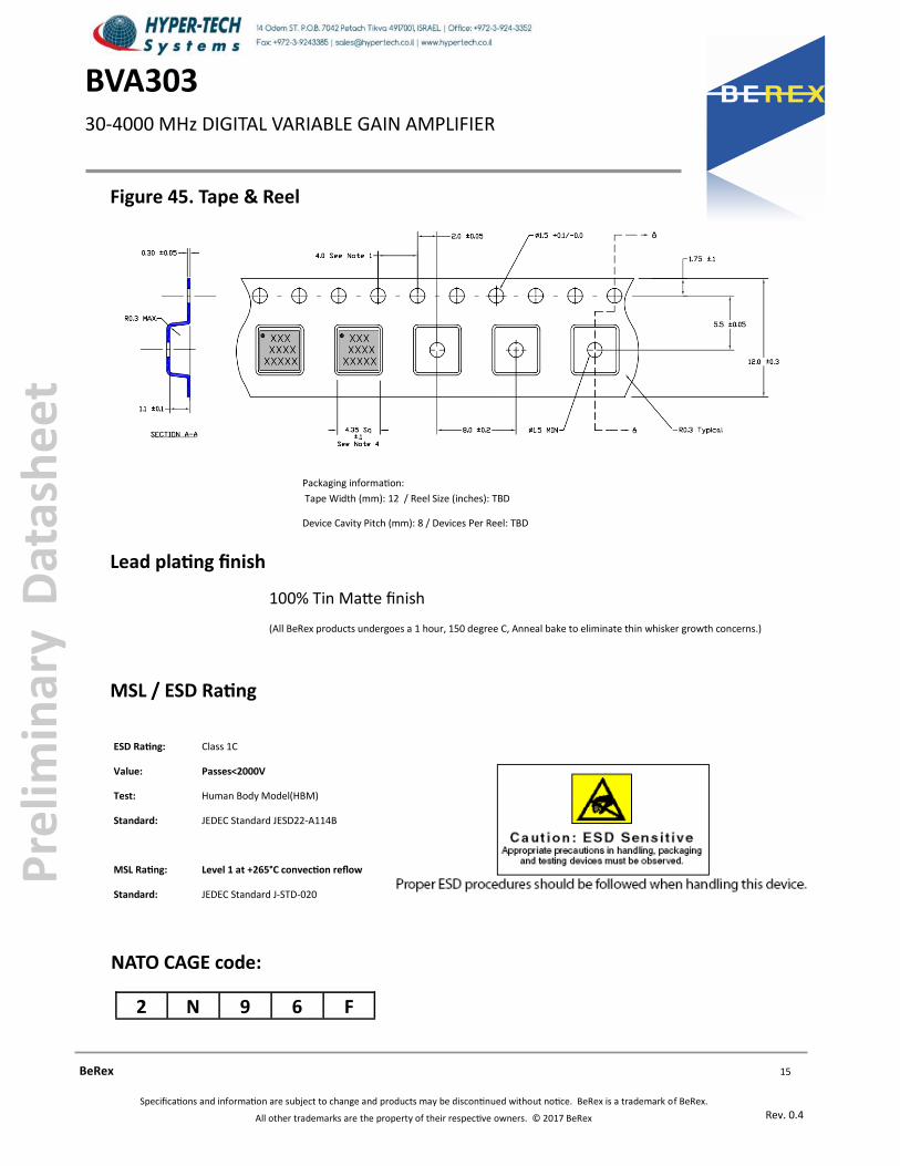
Figure 45. Tape & Reel
Lead plating finish
100% Tin Matte finish
(All BeRex products undergoes a 1 hour, 150 degree C, Anneal bake to eliminate thin whisker growth concerns.)
MSL / ESD Rating
ESD Rating:
Value:
Test:
Standard:
MSL Rating:
Standard:
Class 1C
Passes<2000V
Human Body Model(HBM)
JEDEC Standard JESD22-A114B
Level 1 at +265°C convection reflow
JEDEC Standard J-STD-020
Packaging information:
Tape Width (mm): 12 / Reel Size (inches): TBD
Device Cavity Pitch (mm): 8 / Devices Per Reel: TBD
NATO CAGE code:
2 N 9 6 F