Embed Size (px)
Citation preview

MIL-STD-883-3 16 September 2019 SUPERSEDING MIL-STD-883K
w/CHANGE 3 3 May 2018
DEPARTMENT OF DEFENSE
TEST METHOD STANDARD
ELECTRICAL TESTS (DIGITAL) FOR MICROCIRCUITS
PART 3: TEST METHODS 3000-3999
AMSC N/A FSC 5962
DISTRIBUTION STATEMENT A. Approved for public release. Distribution is unlimited.
This document and process conversion measures necessary to comply with this change shall be completed by 16 March 2020.
INCH - POUND
Downloaded from http://www.everyspec.com

MIL-STD-883-3
ii
FOREWORD 1. This standard is approved for use by all Departments and Agencies of the Department of Defense. 2. This entire standard has been revised. This revision has resulted in many changes to the format, but the most significant one is the splitting the document into parts. See MIL–STD–883 for the change summary. 3. Comment, suggestions, or questions on this document should be addressed to: Commander, Defense Logistics Agency, ATTN: DLA Land and Maritime - VA, P.O. Box 3990, Columbus, OH 43218-3990, or by email to [email protected]. Since contact information can change, you may want to verify the currency of this address information using the ASSIST Online database at: https://assist.dla.mil/.
Downloaded from http://www.everyspec.com

MIL-STD-883-3
iii
CONTENTS
PARAGRAPH Page
1. SCOPE ............................................................................................................................... 1 1.1 Purpose ............................................................................................................................ 1 1.2 Numbering system ........................................................................................................... 1
2. APPLICABLE DOCUMENTS ............................................................................................. 1 2.1 General ............................................................................................................................. 1 2.2 Government documents ................................................................................................... 1 2.3 Non-Government publications .......................................................................................... 3 2.4 Order of precedence ........................................................................................................ 5
3. DEFINITIONS ..................................................................................................................... 5 3.1 Abbreviations, symbols, and definitions............................................................................ 5
4. GENERAL REQUIREMENTS ............................................................................................ 8 4.1 General ............................................................................................................................. 8 4.2 Test circuits ...................................................................................................................... 8 4.3 Destructive tests ............................................................................................................... 8 4.4 Laboratory suitability ........................................................................................................ 8 4.5 Method of reference ......................................................................................................... 8
5. DETAIL REQUIREMENTS ................................................................................................. 8
6. NOTES ............................................................................................................................... 8 6.1 Intended use ..................................................................................................................... 8 6.2 International standardization agreement .......................................................................... 8 6.3 Subject term (key word) listing ......................................................................................... 8 6.4 Supersession data ............................................................................................................ 8
Downloaded from http://www.everyspec.com

MIL-STD-883-3
iv
ELECTRICAL TESTS (DIGITAL)
3001.1 Drive source, dynamic 3002.1 Load conditions 3003.1 Delay measurements 3004.1 Transition time measurements 3005.1 Power supply current 3006.1 High level output voltage 3007.1 Low level output voltage 3008.1 Breakdown voltage, input or output 3009.1 Input current, low level 3010.1 Input current, high level 3011.1 Output short circuit current 3012.1 Terminal capacitance 3013.2 Noise margin measurements for digital microelectronic devices 3014 Functional testing 3015.9 Electrostatic discharge sensitivity classification 3016.1 Activation time verification 3017 Microelectronics package digital signal transmission 3018 Crosstalk measurements for digital microelectronic device packages 3019.2 Ground and power supply impedance measurements for digital microelectronics device
packages 3020 High impedance (off-state) low-level output leakage current 3021 High impedance (off-state) high-level output leakage current 3022 Input clamp voltage 3023.2 Static latch-up measurements for digital CMOS microelectronic devices 3024 Simultaneous switching noise measurements for digital microelectronic devices
Downloaded from http://www.everyspec.com

MIL-STD-883-3
1
1. SCOPE
1.1 Purpose. Part 3 of this test method standard establishes uniform test methods for the electrical testing (digital)
to determine resistance to deleterious effects of natural elements and conditions surrounding military operations. For the purpose of this standard, the term "devices" includes such items as monolithic, multichip, film and hybrid microcircuits, microcircuit arrays, and the elements from which the circuits and arrays are formed. This standard is intended to apply only to microelectronic devices.
1.2 Numbering system. The test methods are designated by numbers assigned in accordance with the following system:
1.2.1 Classification of tests. The electrical test methods included in this part of a multipart test method standard are numbered 3001 to 3024 inclusive.
1.2.2 Test method revisions. Revisions are numbered consecutively using a period to separate the test method number and the revision number. For example, 3001.2 designates the second revision of test method 3001. 2. APPLICABLE DOCUMENTS 2.1 General. The documents listed in this section are specified in sections 3, 4, and 5 of this standard. This section does not include documents cited in other sections of this standard or recommended for additional information or as examples. While every effort has been made to ensure the completeness of this list, document users are cautioned that they must meet all specified requirements documents cited in sections 3, 4, and 5 of this standard, whether or not they are listed. 2.2 Government documents. 2.2.1 Specifications, standards, and handbooks. The following specifications, standards, and handbooks form a part of this document to the extent specified herein. Unless otherwise specified, the issues of these documents are those cited in the solicitation or contract. DEPARTMENT OF DEFENSE SPECIFICATIONS
MIL-PRF-680 - Degreasing Solvent, Performance Specification For. MIL-PRF-19500 - Semiconductor Devices, General Specification For. MIL-PRF-38534 - Hybrid Microcircuits, General Specification For. MIL-PRF-38535 - Integrated Circuits (Microcircuits) Manufacturing, General Specification For.
DEPARTMENT OF DEFENSE STANDARDS
MIL-STD-202 - Electronic and Electrical Component Parts. MIL-STD-750 - Test Methods for Semiconductor Devices. MIL-STD-1686 - Electrostatic Discharge Control Program for Protection of Electrical and Electronic
Parts, Assemblies and Equipment (Excluding Electrically Initiated Explosive Devices).
MIL-STD-1835 - Electronic Component Case Outlines. MIL-STD-1916 - DOD Preferred Methods for Acceptance of Product.
DEPARTMENT OF DEFENSE HANDBOOKS
MIL-HDBK-217 - Reliability Prediction of Electronic Equipment. MIL-HDBK-505 - Definitions of Item Levels, Item Exchangeability, Models, and Related Terms. MIL-HDBK-781 - Reliability Test Methods, Plans, and Environments for Engineering, Development
Qualification, and Production . MIL-HDBK-1331 - Parameters to be Controlled for the Specification of Microcircuits.
Downloaded from http://www.everyspec.com

MIL-STD-883-3
2
FEDERAL STANDARDS SAE AMS-STD-595 - Colors Used in Government Procurement SAE AMS-STD-595/15102 - Blue, Gloss SAE AMS-STD-595/25102 - Blue, Semi-gloss OTHER GOVERNMENT DOCUMENTS, DRAWINGS, AND PUBLICATIONS QML-38534 - Hybrid Microcircuits, General Specification For.
QML-38535 - Integrated Circuits (Microcircuits) Manufacturing, General Specification For. COMMERCIAL ITEM DESCRIPTIONS A-A-58092 - Tape, Antiseize, Polytetrafluorethylene. (Copies of these documents are available online at https://quicksearch.dla.mil.)
Downloaded from http://www.everyspec.com

MIL-STD-883-3
3
2.3 Non-Government publications. The following documents form a part of this document to the extent specified herein. Unless otherwise specified, the issues of these documents are those cited in the solicitation or contract.
INTERNATIONAL ORGANIZATION FOR STANDARDIZATION (ISO) STANDARDS
ISO 14644-1 - Cleanrooms and Associated Controlled Environments – Part 1: Classification of Air Cleanliness.
ISO 14644-2 - Cleanrooms and Associated Controlled Environments – Part 2: Specifications for Testing and Monitoring to Prove Continued Compliance with ISO 14644-1.
ISO /ASTM 51275 - Standard Practice for Use of a Radiochromic Film Dosimetry System. (Copies of these documents are available online at https://www.iso.org)
AMERICAN NATIONAL STANDARDS INSTITUTE (ANSI) ANSI/NCSL Z540.3 - Requirements for the Calibration of Measuring and Test Equipment,
General Requirements. (Copies of these documents are available online at https://ansi.org) IPC - ASSOCIATION CONNECTING ELECTRONICS INDUSTRIES (IPC)
IPC J-STD-004 - Requirements for Soldering Fluxes. IPC J-STD-005 - Requirements for Soldering Pastes. IPC J-STD-006 - Requirements for Electronic Grade Solder Alloys and Fluxed and Non-fluxed Solid
Solders for Electronic Soldering Applications. IPC J-STD-033 - Handling, Packing, Shipping and Use of Moisture/Reflow Sensitive Surface Mount
Devices. IPC-T-50 - Terms and Definitions for Interconnecting and Packaging Electronic Circuits.
(Copies of these documents are available online at https://www.ipc.org)
JEDEC SOLID STATE TECHNOLOGY ASSOCIATION (JEDEC).
JEDEC JESD22-B116 - Wire Bond Shear Test JEDEC JESD78 - IC Latch-up Test. JEDEC JESD213 - Common Test Method for Detection Component Surface Finish Material. JEDEC Standard 12 - Standard for Gate Array Benchmark Set JEDEC Standard 12-1 - Terms and Definitions for Gate Array Benchmark Set. JEDEC Standard 12-2 - Standard for Cell-Based Integrated Circuit Benchmark Set. JEDEC Standard 12-3 - CMOS Gate Array Macrocell Standard.
(Copies of these documents are available online at https://www.jedec.org)
Downloaded from http://www.everyspec.com

MIL-STD-883-3
4
NATIONAL COUNCIL ON RADIAATION PROTECTION AND MEASUREMENT Report Number 40 - Protection Against Radiation from Brachytherapy Sources Report Number 102 - Medical X-ray, Electron Beam and Gamma Ray Protection (Copies of these documents are available online at http://www.NCRPPublications.org) TECHSTREET THOMPSON REUTERS
TechAmerica EIA-557 - Statistical Process Control Systems.
(Copies of these documents are available online at https://www.techstreet.com) AMERICAN SOCIETY FOR TESTING AND MATERIALS (ASTM) ASTM C 177 - Standard Test Method for Steady-State Heat Flux Measurements and Thermal
Transmission Properties by Means of the Guarded Hot-Plate Apparatus. ASTM C 518 - Standard Test Method for Steady-State Heat Flux Measurements and Thermal
Transmission Properties by Means of the Heat Flow Meter Apparatus. ASTM D 150 - Standard Test Methods for A-C Loss Characteristics and Permittivity (Dielectric
Constant) of Solid Electrical Insulating Materials. ASTM D 257 - Standard Test Methods for D-C Resistance or Conductance of Insulating Materials. ASTM D 877 - Standard Test Methods for Dielectric Breakdown Voltage of Insulating Liquids
Using Disk Electrodes. ASTM D 971 - Interfacial Tension of Oil Against Water by the Ring Method. ASTM D 1002 - Standard Test Method for Strength Properties of Adhesives in Shear by Tension
Loading (Metal-to-Metal). ASTM D 1120 - Engine Coolant, Boiling Point of. ASTM D 1331 - Standard Test Methods for Surface and Interfacial Tension of Solutions of Surface-
Active Agents. ASTM D 2109 - Standard Test Methods for Nonvolatile Matter in Halogenated Organic Solvents and
their Admixtures. ASTM D 3574 - Materials, Flexible Cellular-Slab, Bonded, and Molded Uretane Foam. ASTM D 3850 - Rapid Thermal Degradation of Solid Electrical Insulating Materials by
Thermogravimetric Method, Test Method for. ASTM E 263 - Standard Test Method for Measuring Fast-Neutron Reaction Rates by
Radioactivation of Iron. ASTM E 264 - Standard Test Method for Measuring Fast-Neutron Reaction Rates by
Radioactivation of Nickel. ASTM E 265 - Standard Test Method for Measuring Reaction Rates and Fast-Neutron Fluences by
Radioactivation of Sulfur-32. ASTM E 666 - Standard Practice for Calculating Absorbed Dose from Gamma or X-Radiation. ASTM E 668 - Standard Practice for Application of Thermoluminescence-Dosimetry (TLD) Systems
for Determining Absorbed Dose on Radiation Hardness Testing of Electronic Devices.
ASTM E 720 - Standard Guide for Selection and Use of Neutron Sensors for Determining Neutron Spectra Employed in Radiation-Hardness Testing of Electronics.
ASTM E 721 - Standard Method for Determining Neutron Energy Spectra with Neutron-Activation Foils for Radiation-Hardness Testing of Electronics.
ASTM E 722 - Standard Practice for Characterizing Neutron Energy Fluence Spectra in Terms of an equivalent Monoenergetic Neutron Fluence for Radiation-Hardness Testing of Electronics.
Downloaded from http://www.everyspec.com

MIL-STD-883-3
5
AMERICAN SOCIETY FOR TESTING AND MATERIALS (ASTM) (CONTINUED)
ASTM E 801 - Standard Practice for Controlling Quality of Radiological Examination of Electronic
Devices. ASTM E 831 - Standard Test Method for Linear Thermal Expansion of Solid Materials by
Thermomechanical Analysis ASTM E 1249 - Minimizing Dosimetry Errors in Radiation Hardness Testing of Silicon Electronic
Devices. ASTM E 1250 - Standard Method for Application of Ionization Chambers to Assess the Low Energy
Gamma Component of Cobalt 60 Irradiators Used in Radiation Hardness Testing of Silicon Electronic Devices.
ASTM E 2450 - Standard Practice for Application of CaF2(Mn) Thermoluminescence Dosimeters in Mixed Neutron-Photon Environments.
ASTM F 458 - Standard Practice for Nondestructive Pull Testing of Wire Bonds. ASTM F 459 - Standard Test Methods for Measuring Pull Strength of Microelectronic Wire Bonds.
ASTM F 526 - Standard Test Method for Measuring Dose for Use in Linear Accelerator Pulsed Radiation Effects Tests.
ASTM F 1192 - Standard Guide for the Measurement of Single Event Phenomena (SEP). ASTM F 1892 - Standard Guide for Ionizing Radiation (Total Dose) Effects Testing of Semiconductor
Devices. (Copies of these documents are available online at https://www.astm.org/) 2.4 Order of precedence. Unless otherwise noted herein or in the contract, in the event of a conflict between the text of this document and the references cited herein, the text of this document takes precedence. Nothing in this document, however, supersedes applicable laws and regulations unless a specific exemption has been obtained.
3. DEFINITIONS
3.1 Abbreviations, symbols, and definitions. For the purpose of this standard, the abbreviations, symbols, and definitions specified in MIL-PRF-19500, MIL-PRF-38535, or MIL-HDBK-505 apply. The following definitions also apply:
3.1.1 Microelectronic device. A microcircuit, microcircuit module, or an element of a microcircuit as defined in appendix A of MIL-PRF-38535. For the purposes of this document, each type of microelectronic device will be identified by a unique type, or drawing number.
3.1.2 Mode of failure. The cause for rejection of any failed device or microcircuit as defined in terms of the specific electrical or physical requirement which it failed to meet (i.e., no failure analysis is required to identify the mode of failure, which should be obvious from the rejection criteria of the test method).
3.1.3 Mechanism of failure. The original defect which initiated the microcircuit or device failure or the physical process by which the degradation proceeded to the point of failure, identifying quality defects, internal, structural, or electrical weakness and, where applicable, the nature of externally applied stresses which led to failure.
Downloaded from http://www.everyspec.com

MIL-STD-883-3
6
3.1.4 Absolute maximum ratings. The values specified for ratings, maximum ratings, or absolute maximum ratings are based on the "absolute system" and are not to be exceeded under any measurable or known service or conditions. In testing microelectronic devices, limits may be exceeded in determining device performance or lot quality, provided the test has been determined to be nondestructive and precautions are taken to limit device breakdown and avoid conditions that could cause permanent degradation. These ratings are limiting values beyond which the serviceability of any individual microelectronic integrated circuit may be impaired. It follows that a combination of all the absolute maximum ratings cannot normally be attained simultaneously. Combinations of certain ratings are permissible only if no single maximum rating is exceeded under any service condition. Unless otherwise specified, the voltage, current, and power ratings are based on continuous dc power conditions at free air ambient temperature of 25C ±3C. For pulsed or other conditions of operation of a similar nature, the current, voltage, and power dissipation ratings are a function of time and duty cycle. In order not to exceed absolute ratings, the equipment designer has the responsibility of determining an average design value, for each rating, below the absolute value of that rating by a safety factor, so that the absolute values will never be exceeded under any usual conditions of supply-voltage variations, load variations, or manufacturing variations in the equipment itself.
3.1.5 Worst case condition. Worst case condition(s) consists of the simultaneous application of the most adverse (in terms of required function of the device) values (within the stated operating ranges) of bias(es), signal input(s), loading and environment to the device under test. Worst cases for different parameters may be different. If all the applied test conditions are not established at the most adverse values, the term "partial worst case condition" should be used to differentiate and should be accompanied by identification of the departure from worst case. For example, the lowest values of supply voltages, signal input levels, and ambient temperature and the highest value of loading may constitute "worst case conditions" for measurement of the output voltage of a gate. Use of the most adverse values of applied electrical conditions, at room temperature, would then constitute "partial worst case conditions" and should be so identified using a postscript "at room temperature."
3.1.5.1 Accelerated test condition. Accelerated test conditions are defined as test conditions using one or more applied stress levels which exceed the maximum rated operating or storage stress levels but are less than or equal to the "Testing Rating" values.
3.1.6 Static parameters. Static parameters are defined as dc voltages, dc currents, or ratios of dc voltages or dc currents, or both.
3.1.7 Dynamic parameters. Dynamic parameters are defined as those which are rms or time-varying values of voltages or currents, or ratios of rms or time-varying values of voltages or currents, or both.
3.1.8 Switching parameters. Switching parameters are defined as those which are associated with the transition of the output from one level to another or the response to a step input.
3.1.9 Functional tests. Functional tests are defined as those go, no-go tests which sequentially exercise a function (truth) table or in which the device is operated as part of an external circuit and total circuit operation is tested.
Downloaded from http://www.everyspec.com
MIL-STD-883-3
7
3.1.10 Acquiring activity. The acquiring activity is the organizational element of the Government which contracts for articles, supplies, or services; or it may be a contractor or subcontractor when the organizational element of the Government has given specific written authorization to such contractor or subcontractor to serve as agent of the acquiring activity. A contractor or subcontractor serving as agent of the acquiring activity does not have the authority to grant waivers, deviations, or exceptions unless specific written authorization to do so has also been given by the Government organization.
3.1.11 Accuracy. The quality of freedom from error. Accuracy is determined or assured by calibration, or reliance upon calibrated items.
3.1.12 Calibration. Comparison of measurement standard or instrument of known accuracy with another standard, instrument or device to detect, correlate, report or eliminate by adjustment, any variation in the accuracy of the item being compared. Use of calibrated items provide the basis for value traceability of product technical specifications to national standard values. Calibration is an activity related to measurement and test equipment performed in accordance with ANSI/NCSL Z540.3 or equivalent.
3.1.13 Precision. The degree to which an instrument, device, assemblage, test, measurement or process exhibits repeatability. Expressed statistically or through various techniques of Statistical Process Control (SPC). Term is used interchangeably with "repeatability".
3.1.14 Resolution. The smallest unit of readability or indication of known value in an instrument, device or assemblage thereof.
3.1.15 Standard reference material (SRM). A device or artifact recognized and listed by the National Institute of Standards and Technology (NIST) as having known stability and characterization. SRM's used in product testing provide traceability for technical specifications. SRM's do not require calibration when used and stored in accordance with NIST accompanying instructions. They are used as "certified materials".
3.1.16 Tolerance. A documented range over which a specified value may vary.
3.1.17 Test accuracy ratio (TAR). A ratio of the tolerance of the device under test to the accuracy of the related measuring or test instrument or to the accuracy of the correlation device/SRM.
3.1.18 Uncertainty. An expression of the combined errors in a test measurement process. Stated as a range within which the subject quantity is expected to lie. Comprised of many components including: estimates of statistical distribution and results of measurement or engineering analysis. Uncertainty established with a suitable degree of confidence, may be used in assuring or determining product conformance and technical specifications.
3.1.19 Susceptibility. The point at which a device fails to meet the postirradiation end-point electrical parameter limits or fails functionally during radiation exposure (e.g., neutron irradiation).
3.1.20 Class M. Class M is defined as 1.2.1 of MIL-STD-883 basic compliant product or product built in compliance to Appendix A of MIL-PRF-38535 documented on a Standard Microcircuit Drawing where configuration control is provided by the Government preparing activity. Class M devices are required to use the conditions specified in the test methods herein for class level B product.
3.1.21 Class level B and class level S. 2 class levels are used in this document to define requirements for high reliability military applications (Class level B) and space applications (Class level S). Class level B requirements contained in this document are intended for use for Class Q, Class H, and Class M products, as well as Class B M38510 JAN slash sheet product. Class level B requirements are also intended for use for product claimed as 883 compliant or 1.2.1 compliant for high reliability military applications. Class level S requirements contained in this document are intended for use for Class V, Class K, as well as M38510 Class S JAN slash sheet product. Class level S requirements are also intended for use for product claimed as 883 compliant or 1.2.1 of MIL-STD-883 basic compliant for space level applications.
Downloaded from http://www.everyspec.com
MIL-STD-883-3
8
3.1.22 Acquisition documents. Acquisition documents consist of the acquisition order or contract, device specification (e.g. SMD’s, SCD’s) or specifications as applicable.
4. GENERAL REQUIREMENTS
4.1 General. Unless otherwise specified in the individual test method, the general requirements of MIL-STD-883 shall apply.
4.2 Test circuits. The test circuits shown in the test methods of this test method standard are given as examples which may be used for the measurements. They are not necessarily the only test circuits which can be used; however the manufacturer shall demonstrate to the Government that other test circuits which they may desire to use will give results within the desired accuracy of measurement.
4.3 Destructive tests. Unless otherwise demonstrated, the test methods listed in table I shall be classified as destructive. MIL-STD-883 covers the necessary actions needed to reclassify a test method as non-destructive.
TABLE I. Destructive tests.
Test method number Test
3015 Electrostatic discharge sensitivity
classification
4.4 Laboratory suitability. Prior to processing any microcircuit intended for use in any military system or sub-system, the facility performing the test(s) shall be audited by the DLA Land and Maritime, Sourcing and Qualification Division and be granted written laboratory suitability status for each test method to be employed. Processing of any devices by any facility without laboratory suitability status for the test methods used shall render the processed devices nonconforming.
4.5 Method of reference. When applicable, test methods contained herein shall be referenced in the individual specification or specification sheet by specifying the test method number and, the details required in the summary of the applicable test method shall be listed. To avoid the necessity for changing documents that refer to test methods of this standard, the revision number should not be used when referencing test methods. (For example: Use 1001 versus 1001.2.)
5. DETAILED REQUIREMENTS
This section is not applicable to this standard.
Downloaded from http://www.everyspec.com

MIL-STD-883-3
9
6. NOTES
(This section contains information of a general or explanatory nature that may be helpful, but is not mandatory.)
6.1 Intended use. The intended use of this test method standard is to establish appropriate conditions for testing semiconductor devices to give test results that simulate the actual service conditions existing in the field. This test method standard has been prepared to provide uniform test methods, controls, and procedures for determining with predictability the suitability of such devices within military, aerospace and special application equipment.
6.2 International standardization agreement. Certain provisions of this test method standard are the subject of international standardization agreement. When amendment, revision, or cancellation of this test method standard is proposed which will affect or violate the international agreement concerned, the preparing activity will take appropriate reconciliation action through international standardization channels, including departmental standardization offices, if required.
6.3 Subject term (key word) listing
Destructive tests Environmental tests Laboratory suitability Non–destructive tests
6.4 Supersession data The main body and five parts (–1 through –5) of this revision of MIL-STD-883 replace
superseded MIL–STD–883K
Downloaded from http://www.everyspec.com

MIL-STD-883-3
10
This page intentionally left blank
Downloaded from http://www.everyspec.com

MIL-STD-883-3
METHOD 3001.1 15 November 1974
1
METHOD 3001.1 DRIVE SOURCE, DYNAMIC 1. PURPOSE. This method establishes a drive source to be used in measuring dynamic performance of digital microelectronic devices, such as TTL, DTL, RTL, ECL, and MOS. 2. APPARATUS. The drive source shall supply a smooth transition between specified voltage levels. The signal characteristics shall not vary outside of their prescribed tolerances when interfaced with the device under test (device in the test socket). 3. PROCEDURE. The drive source shall be measured at the input terminal of the test socket (no device in the test socket). Figure 3001-1 shows typical driving source waveforms and should be used specifying the parameters shown, unless otherwise stated in the applicable acquisition document. 3.1 Pulse amplitude. The specified HIGH level of the driving source shall be greater than the VOH of the device. The specified LOW level of the driving source shall be less than VOL of the device. 3.2 Transition times. The transition times of the driving source (tTHL and tTLH) shall be faster than the transition time of the device being tested, unless otherwise stated in the acquisition document. The transition times shall normally be measured between the 10 percent and 90 percent levels of the specified pulse. 3.3 Pulse repetition rate (PRR). Unless the pulse repetition rate is the parameter being tested, it shall be chosen so that doubling the rate or reducing by a half will not affect the measurement results. 3.4 Duty factors (duty cycles). The duty cycles of the driving source shall be chosen so that a 10 percent variation in the duty cycle will not affect the measurement results. The duty cycle shall be defined with respect to either a positive or negative pulse. The pulse width (tp) of the input pulses shall be measured between the specified input measurement levels. When more than one pulse input is needed to test a device, the duty cycle of the prime input (i.e., clock, etc.) shall be specified. The phase relationship of all other input pulses shall be referenced to the prime input pulse. 4. SUMMARY. The following details, when applicable, shall be specified in the applicable acquisition document:
a. Levels VIL and VIH.
b. Driving signal transition times.
c. Pulse repetition rate.
d. Duty factors.
e. Recommended pulse generator, if required.
f. Input measurement levels, if other than those shown in figure 3001-1.
Downloaded from http://www.everyspec.com

MIL-STD-883-3
METHOD 3001.1 15 November 1974
2
FIGURE 3001-1. Drive sources.
Downloaded from http://www.everyspec.com

MIL-STD-883-3
METHOD 3002.1 15 November 1974
1
METHOD 3002.1 LOAD CONDITIONS 1. PURPOSE. This method establishes the load conditions to be used in measuring the static and dynamic performance of digital microelectronic devices such as TTL, DTL, RTL, ECL, and MOS. 2. APPARATUS. The load for static tests shall simulate the worst case conditions for the circuit parameters being tested. The load for dynamic tests shall simulate a specified use condition for the parameters being tested. The loads shall be specified in the applicable acquisition document. 2.1 Discrete component load. The load will consist of any combination of capacitive, inductive, resistive, or diode components. 2.1.1 Capacitive load (CL). The total load capacitance of the circuit under test shall include probe and test fixture capacitance and a compensating capacitor as required. The value of the capacitance, measured at 1 MHz ±10 percent, shall be specified in the applicable acquisition document. 2.1.2 Inductive load (LL). The total load inductance of the circuit under test shall include probe and test fixture inductance and a compensating inductor as required. The value of the inductance, measured at 1 MHz ±10 percent, shall be specified in the applicable acquisition document. 2.1.3 Resistive load (RL). The resistive load shall represent the worst case fan out conditions of the device under test for static tests and a specified fan out condition for dynamic tests. For sink loads, the resistor shall be connected between the power supply (VCC or VDD) and the circuit output for TTL, DTL, RTL, C-MOS, and MOS (N-Channel) and between circuit output and ground for MOS (P-Channel). For source loads, the resistor shall be connected between circuit output and ground for TTL, DTL, RTL, C-MOS, and MOS (N-Channel) and between VDD and the circuit output for MOS (P-Channel). For ECL devices, the load resistors are connected from the output to a specified negative voltage. 2.1.4 Diode load (DL). The diode load shall represent the input diode(s) of the circuit under test. The equivalent diode, as specified in the applicable acquisition document, will also represent the base-emitter or base-collector diode of any transistor in the circuit path of the normal load. 2.2 Dynamic load change. The load shall automatically change its electrical parameters as the device under test changes logic state if this is the normal situation for the particular family of circuits being tested. One method of accomplishing this dynamic change is to simulate devices or use actual devices from the same logic family equal to the specified load. 3. PROCEDURE. The load will normally be paralleled by a high impedance voltage detection indicator. The indicator may be either visual or memory storage. 4. SUMMARY. The following shall be defined in the applicable acquisition document:
a. Capacitive load (see 2.1.1).
b. Inductive load (see 2.1.2).
c. Resistive load (see 2.1.3).
d. Diode load, the 1NXXX number and any associated critical parameters shall be specified (see 2.1.4).
e. Negative voltage, when using a resistive load for ECL (see 2.1.3).
Downloaded from http://www.everyspec.com

MIL-STD-883-3
METHOD 3002.1 15 November 1974
2
This page intentionally left blank
Downloaded from http://www.everyspec.com

MIL-STD-883-3
METHOD 3003.1 15 November 1974
1
METHOD 3003.1 DELAY MEASUREMENTS 1. PURPOSE. This method established the means for measuring propagation delay of digital microelectronic devices, such as TTL, DTL, RTL, ECL, and MOS. 1.1 Definitions. The following definitions for the purpose of this test method shall apply. 1.1.1 Propagation delay time (tPHL). The time measured with the specified output changing from the defined HIGH level to the defined LOW level with respect to the corresponding input transition. 1.1.2 Propagation delay time (tPLH). The time measured with the specified output changing from the defined LOW level to the defined HIGH level with respect to the corresponding input transition. 2. APPARATUS. Equipment capable of measuring elapsed time between the input signal and output signal at any percentage point or voltage point between the maximum LOW level and minimum HIGH level shall be provided. The input shall be supplied by a driving source as described in method 3001 of this standard. It is desirable for this equipment to have data logging capability so that circuit dynamic performance can be monitored. The test chamber shall be capable of maintaining the device under test at any specified temperature. 3. PROCEDURE. The test circuit shall be loaded according to method 3002 of this standard. The driving signal to the test circuit shall be provided according to method 3001 of this standard. The device shall be stabilized at the specified test temperature. 3.1 Measurements at a voltage point. tPLH and tPHL shall be measured from the threshold voltage point on the driving signal to the threshold voltage point on the test circuit output signal for both inverting and noninverting logic. These delays shall be measured at the input and output terminals of the device under test. The device under test shall be conditioned according to the applicable acquisition document with nominal bias voltages applied. Figures 3003-1 and 3003-2 show typical delay measurements. 3.2 Measurements at percentage points. tPLH and tPHL shall be measured from a specified percentage point on the driving signal to a specified percentage point on the test circuit output signal for both inverting and noninverting logic. These delays shall be measured at the input and output terminals of the device under test. The device under test shall be conditioned according to the applicable acquisition document with nominal bias voltages applied. Figures 3003-1 and 3003-2 show typical delay measurements. 4. SUMMARY. The following details shall be specified in the applicable acquisition document:
a. tPLH and tPHL limits.
b. Parameters of the driving signal: tTHL, tTLH, high Level, low Level, pulse width, repetition rate.
c. Load conditions.
d. Conditioning voltages (static or dynamic).
e. Measurement points (see 3.1 and 3.2).
f. Power supply voltages.
g. Test temperature.
Downloaded from http://www.everyspec.com

MIL-STD-883-3
METHOD 3003.1 15 November 1974
2
FIGURE 3003-1. Propagation delay-positive input pulse.
Downloaded from http://www.everyspec.com

MIL-STD-883-3
METHOD 3003.1 15 November 1974
3
FIGURE 3003-2. Propagation delay - negative input pulse.
Downloaded from http://www.everyspec.com

MIL-STD-883-3
METHOD 3003.1 15 November 1974
4
This page intentionally left blank
Downloaded from http://www.everyspec.com

MIL-STD-883-3
METHOD 3004.1 15 November 1974
1
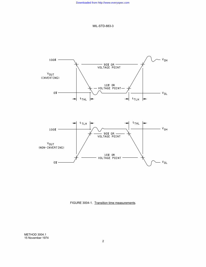
METHOD 3004.1 TRANSITION TIME MEASUREMENTS 1. PURPOSE. This method establishes the means for measuring the output transition times of digital microelectronic devices, such as TTL, DTL, RTL, ECL, and MOS. 1.1 Definitions. The following definitions shall apply for the purpose of this method. 1.1.1 Rise time (tTLH). The transition time of the output from 10 percent to 90 percent or voltage levels of output voltage with the specified output changing from the defined LOW level to the defined HIGH level. 1.1.2 Fall time (tTHL). The transition time of the output from 90 percent to 10 percent or voltage levels of output voltage with the specified output changing from the defined HIGH level to the defined LOW level. 2 APPARATUS. Equipment capable of measuring the elapsed time between specified percentage points (normally 10 percent to 90 percent on the positive transition and 90 percent to 10 percent on the negative transition) or voltage levels. The test chamber shall be capable of maintaining the device under test at any specified temperature. 3. PROCEDURE. The device shall be stabilized at the specified test temperature. The device under test shall be loaded as specified in the applicable acquisition document. The load shall meet the requirements specified in method 3002 of this document. The driving signal shall be applied as specified in method 3001 or the applicable acquisition document. 3.1 Measurement of tTLH and tTHL. Unless otherwise stated, the rise transition time (tTLH) shall be measured between the 10 percent and 90 percent points on the positive transition of the output pulse and the fall transition time (tTHL) shall be measured between the 90 percent and 10 percent points on the negative transition of the output pulse. The device under test shall be conditioned according to the applicable acquisition document with nominal bias voltages applied. Figure 3004-1 shows typical transition time measurement. 4. SUMMARY. The following details shall be specified in the applicable acquisition document:
a. tTLH limits.
b. tTHL limits. c. Transition time measurement points if other than 10 percent or 90 percent.
d. Parameters of the driving signal.
e. Conditioning voltages (static or dynamic).
f. Load condition.
g. Power supply voltages.
h. Test temperature.
Downloaded from http://www.everyspec.com
MIL-STD-883-3
METHOD 3004.1 15 November 1974
2
FIGURE 3004-1. Transition time measurements.
Downloaded from http://www.everyspec.com

MIL-STD-883-3
METHOD 3005.1 15 November 1974
1
METHOD 3005.1 POWER SUPPLY CURRENT 1. PURPOSE. This method establishes the means for measuring power supply currents of digital microelectronic devices such as TTL, DTL, RTL, ECL, and MOS. 2. APPARATUS. Equipment capable of applying prescribed voltage to the test circuit power supply terminals and measuring the resultant currents flowing in these terminals shall be provided. The test chamber shall be capable of maintaining the device under test at any specified temperature. 3. PROCEDURE. The device shall be stabilized at the specified test temperature. 3.1 ICCH (logic gate). Inputs of the device under test shall be conditioned in such a way as to provide a HIGH level at the output, the worst case supply voltage(s) shall be applied and the resultant current flow in the supply terminals measured. 3.2 ICCL (logic gate). Inputs of the device under test shall be conditioned in such a way as to provide a LOW level at the output, the worst case supply voltages(s) shall be applied and the resultant current flow in the supply terminals measured. 3.3 ICC or IEE of combinatorial digital circuits. The inputs of the device under test shall be conditioned to put the device into its worst case power dissipating state. The current flowing into the VCC, (positive supply) terminal, or out of the VEE (negative supply) terminal shall be measured with the VCC and VEE voltages at their maximum specified operating levels. 3.4 ICC or IEE of sequential digital circuits. The inputs of the device under test shall be exercised to put the device in a known output state (either HIGH or LOW) that causes worst case power dissipation. The current flowing into the VCC (positive supply) terminal, or out of the VEE (negative supply) terminal shall be measured with the VCC and VEE voltages at their maximum specified operating levels. 3.5 IDD (MOS logic gate). Inputs of the device under test shall be conditioned in such a way as to provide a HIGH level at the output of MOS (P-Channel and C-MOS) or a LOW level at the output of MOS (N-Channel and C-MOS); worst case voltage(s) shall be applied and the resultant current in the supply terminals measured. 3.6 IGG (MOS P-Channel and N-Channel logic gates). Inputs of the device under test shall be conditioned in such a way as to provide a HIGH level at the output of MOS (P-Channel) or a LOW level at the output of MOS (N-Channel); worst case voltage(s) shall be applied and the resultant current flow in the supply terminals measured. 3.7 IDD of MOS combinatorial circuits. See 3.3 above. 3.8 IDD of MOS sequential circuits. See 3.4 above. 3.9 IGG of MOS combinatorial circuits. See 3.3 above. 3.10 IGG of MOS sequential circuits. See 3.4 above. 3.11 IDD dynamic (MOS logic gating and flip flop circuits). The driving signal to the test circuit shall be provided according to method 3001 of this standard; the worst case voltage(s) shall be applied and the resultant average current in the supply terminals measured.
Downloaded from http://www.everyspec.com

MIL-STD-883-3
METHOD 3005.1 15 November 1974
2
4. SUMMARY. The following details shall be specified in the applicable acquisition document:
a. Test temperature.
b. Power supply voltages.
c. ICCH, ICCL, IDD, IGG, and IEE limits.
d. Conditioning voltages.
e. Dynamic input parameters (see 3.11).
Downloaded from http://www.everyspec.com

MIL-STD-883-3
METHOD 3006.1 15 November 1974
1
METHOD 3006.1 HIGH LEVEL OUTPUT VOLTAGE 1. PURPOSE. This method establishes the means for assuring circuit performance to the limits specified in the applicable acquisition document in regard to HIGH level output drive, which may be specified as a minimum value VOH min. or as a maximum VOH max. This method applies to digital microelectronic devices, such as TTL, DTL, RTL, ECL, and MOS. 2. APPARATUS. The test instrument shall be capable of loading the output of the circuit under test with the specified positive or negative currents (IOH). Resistors may be used to simulate the applicable current levels. The test instrument shall also be capable of supplying the worst case power supply and input voltages. The test chamber shall be capable of maintaining the device under test at any specified test temperature. 3. PROCEDURE. The device shall be stabilized at the specified test temperature. Worst case power supply voltages and worst case input levels including guaranteed noise margins shall be applied to the test circuit to provide a HIGH level output. Forcing current, equal to the circuit worst case high level fan out, shall then be applied to the test circuit output terminal and the resultant output voltage measured. The output measurement shall be made after each input is conditioned. 4. SUMMARY. The following details shall be specified in the applicable acquisition document:
a. Test temperature.
b. Current to be forced from or into output terminal.
c. Power supply voltage(s).
d. Input levels.
e. VOH min. or VOH max. limits.
Downloaded from http://www.everyspec.com

MIL-STD-883-3
METHOD 3006.1 15 November 1974
2
This page intentionally left blank
Downloaded from http://www.everyspec.com

MIL-STD-883-3
METHOD 3007.1 15 November 1974
1
METHOD 3007.1 LOW LEVEL OUTPUT VOLTAGE 1. PURPOSE. This method establishes the means for assuring circuit performance to the limits specified in the applicable acquisition document with regard to LOW level output drive which is specified as a maximum value (VOL max) or a minimum value (VOL min). This method applies to digital microelectronic devices, such as TTL, DTL, RTL, ECL, and MOS. 2. APPARATUS. The test instrument shall be capable of loading the output of the circuit under test with the specified positive or negative currents (IOL). Resistors may be used to simulate the applicable current levels. The test instrument shall be capable of supplying the worst case power supply and input voltages. The test chamber shall be capable of maintaining the device under test at any specified temperature. 3. PROCEDURE. The device shall be stabilized at the specified test temperature. Worst case power supply voltages and worst case input levels including guaranteed noise margins shall be applied to the test circuit to provide a LOW level output. Forcing current, equal to the circuit worst case LOW level fan out, shall be applied to the test circuit output and the resultant output voltage measured. The output measurement shall be made after each input is conditioned. 4. SUMMARY. The following details shall be specified in the applicable acquisition document:
a. Test temperature.
b. Current to be forced into or from the output terminal.
c. Power supply voltage(s).
d. Input levels.
e. VOL max or VOL min limits.
Downloaded from http://www.everyspec.com

MIL-STD-883-3
METHOD 3007.1 15 November 1974
2
This page intentionally left blank
Downloaded from http://www.everyspec.com

MIL-STD-883-3
METHOD 3008.1 15 November 1974
1
METHOD 3008.1 BREAKDOWN VOLTAGE, INPUT OR OUTPUT 1. PURPOSE. This method establishes the means for assuring device performance to the limits specified in the applicable acquisition document in regard to input and output breakdown voltage symbolized as VIH (max), VOH (max), VIL (min), and VOL (min) as applicable. This method applies to digital microelectronic devices, such as TTL, DTL, RTL, ECL, and MOS. 2. APPARATUS. The test chamber shall be capable of maintaining the device under test at any specified temperature. 2.1 Method A. This test is generally performed to assure that breakdown does not occur on a device. An instrument shall be provided that has the capability of forcing a specified voltage at the input or output terminal of the test circuit and measuring the resultant current flowing in that terminal. The test instrument shall also have the capability of applying voltage levels to all other terminals. Care should be taken to assure that the test equipment does not inadvertently apply voltage to the device under test that will exceed the maximum rating of each terminal and that the current from the test equipment is sufficiently limited so that the device is not destroyed. This method can also be used to test the ability of power supply terminals to withstand a voltage overload. 2.2 Method B. This test is generally performed to assure that breakdown does occur on a device as specified in the applicable acquisition document. An instrument shall be provided that has the capability of forcing a specified current at the input or output terminal of the test circuit and measuring the resultant voltage at that terminal. The test instrument shall also have the capability of applying voltage levels to all other terminals. Care should be taken to assure that the test equipment does not inadvertently apply voltage to the device under test that will exceed the maximum rating of each terminal so that the device is not destroyed. The minimum compliance voltage of the current source shall be specified when applicable. 3. PROCEDURE. The device shall be stabilized at the specified test temperature. 3.1 Method A. All terminals, with the exception of the test terminal, shall be conditioned according to the applicable acquisition document. A prescribed voltage shall be applied to the designated input or output terminal and the resultant current measured. When testing for breakdown, all input and output terminals shall be tested individually. At the conclusion of the test, the device shall be functional. 3.2 Method B. All terminals, with the exception of the test terminal, shall be conditioned according to the applicable acquisition document. The specified current shall be forced at the designated input or output terminal, and the voltage at the terminal measured. At the conclusion of the test, the device shall be functional. 4. SUMMARY. The following details shall be specified in the applicable acquisition document:
a. Test temperature.
b. Forced voltages (method A).
c. Conditioning voltages for all other terminals.
d. Forced current (method B).
e. Maximum breakdown current limits (method A).
f. Minimum breakdown terminal voltage (method B).
Downloaded from http://www.everyspec.com

MIL-STD-883-3
METHOD 3008.1 15 November 1974
2
This page intentionally left blank
Downloaded from http://www.everyspec.com

MIL-STD-883-3
METHOD 3009.1 15 November 1974
1
METHOD 3009.1 INPUT CURRENT, LOW LEVEL 1. PURPOSE. This method establishes the means for assuring circuit performance to the limits specified in the applicable acquisition document in regard to LOW level input load which may be specified as a minimum value (IIL min) or as a maximum value (IIL max). This method applied to digital microelectronic devices, such as TTL, DTL, RTL, ECL, and MOS. 2. APPARATUS. The test chamber shall be capable of maintaining the device under test at any specified test temperature. An instrument shall be provided that has the capability of applying the worst case LOW voltage to the input terminal of the test circuit, (and worst case levels on the other inputs), and measuring the resultant current at the input terminal. 3. PROCEDURE. The device shall be stabilized at the specified test temperature. Worst case power supply voltages and worst case input voltages shall be applied to the test circuit and the resultant current at the input terminal shall be measured. Inputs shall be tested individually. 4. SUMMARY. The following details shall be specified in the applicable acquisition document:
a. Test temperature.
b. Power supply voltages.
c. Input voltage.
d. Voltages at other input terminals which cause worst case current at the input under test.
e. IIL max or IIL min.
Downloaded from http://www.everyspec.com
MIL-STD-883-3
METHOD 3009.1 15 November 1974
2
This page intentionally left blank
Downloaded from http://www.everyspec.com
MIL-STD-883-3
METHOD 3010.1 15 November 1974
1
METHOD 3010.1 INPUT CURRENT, HIGH LEVEL 1. PURPOSE. This method establishes the means for assuring circuit performance to the limits specified in the applicable acquisition document in regard to HIGH level input load which may be specified as a maximum value (IIH max) or a minimum value (IIH min). This method applies to digital microelectronic devices, such as TTL, DTL, RTL, ECL, and MOS. 2. APPARATUS. The test chamber shall be capable of maintaining the device under test at any specified temperature. An instrument shall be provided that has the capability of applying the worst case HIGH voltage to the input terminal of the test circuit, and worst case levels at the other inputs, and measuring the resultant current at the input terminal. 3. PROCEDURE. The device shall be stabilized at the specified test temperature. Worst case power supply voltages and worst case input voltages shall be applied to the test circuit and the resultant current at the input terminal shall be measured. Inputs shall be tested individually. 4. SUMMARY. The following details shall be specified in the applicable acquisition document:
a. Test temperature.
b. Power supply voltages.
c. Input voltage.
d. Input voltages at other input terminals which cause worst case current at the input under text.
e. IIH max.
Downloaded from http://www.everyspec.com

MIL-STD-883-3
METHOD 3010.1 15 November 1974
2
This page intentionally left blank
Downloaded from http://www.everyspec.com

MIL-STD-883-3
METHOD 3011.1 15 November 1974
1
METHOD 3011.1 OUTPUT SHORT CIRCUIT CURRENT 1. PURPOSE. This method establishes the means for assuring circuit performance to the limits specified in the applicable acquisition document in regard to output short circuit current (IOS). This method applied to digital microelectronic devices, such as TTL, DTL, RTL, and MOS. 2. APPARATUS. A test chamber capable of maintaining the device under test at any specified temperature. An instrument will be provided that has the capability of forcing a voltage specified in the applicable acquisition document at the output terminal of the device under test and measuring the resultant current flowing in that terminal. The test instrument shall also have the capability of applying specified voltage levels to all other inputs. 3. PROCEDURE. The device shall be stabilized at the specified test temperature. Each output per package shall be tested individually. 3.1 TTL, DTL, RTL, MOS (P-Channel and N-Channel). Inputs of the device under test shall be conditioned in such a way as to provide a HIGH level at the output for TTL, DTL, RTL, and MOS (N-Channel) and a LOW level at the output for MOS (P-Channel). The output terminal shall be forced to 0 volt potential and the resultant current flow measured. 3.2 C-MOS IOSH. Inputs of the device under test shall be conditioned in such a way as to provide a HIGH level at the output. The output terminal shall be forced to 0 volt potential and the resultant current flow measured. 3.3 C-MOS IOSL. Inputs of the device under test shall be conditioned in such a way as to provide a LOW level at the output. The output terminal shall be forced to a voltage potential specified in the acquisition document and the resultant current flow measured. 4. SUMMARY. The following details shall be specified in the applicable acquisition document:
a. Test temperature.
b. Input conditioning voltages.
c. Power supply voltages.
d. IOS max and IOS min limits.
Downloaded from http://www.everyspec.com

MIL-STD-883-3
METHOD 3011.1 15 November 1974
2
This page intentionally left blank
Downloaded from http://www.everyspec.com

MIL-STD-883-3
METHOD 3012.1 15 November 1974
1
METHOD 3012.1 TERMINAL CAPACITANCE 1. PURPOSE. This method establishes the means for assuring circuit performance to the limits specified in the applicable acquisition document in regard to terminal capacitance. This method applies to digital microelectronic devices, such as TTL, DTL, RTL, ECL, and MOS. 2. APPARATUS. The instrument shall be capable of applying a 1 MHz controllable amplitude signal superimposed on a variable plus or minus dc voltage. The instrument will also have the capability of measuring the capacitance of this terminal to within the limits and tolerance specified in the applicable acquisition document. 3. PROCEDURE. This test may be performed at 25C ±3C. The capacitance measuring bridge shall be connected between the input or output terminal and the ground terminal of the test circuit. The bridge shall be adjusted for a signal of 1 MHz, riding a bias level specified in the applicable acquisition document; the signal amplitude shall not exceed 50 mV rms. With no device in the test socket the bridge shall then be zeroed. For capacitance values below 20 pF, the device shall be connected directly to the bridge with leads as short as possible to avoid the effects of lead inductance. After inserting the device under test and applying the specified bias conditions, the terminal capacitance shall be measured and compared to the limits listed in the applicable acquisition document. 4. SUMMARY. The following details shall be specified in the applicable acquisition document:
a. Circuit bias conditions.
b. Bias level at which measurements are to be made.
c. Maximum capacitance limits.
Downloaded from http://www.everyspec.com

MIL-STD-883-3
METHOD 3012.1 15 November 1974
2
This page intentionally left blank
Downloaded from http://www.everyspec.com
MIL-STD-883-3
METHOD 3013.2 22 February 2017
1
METHOD 3013.2 NOISE MARGIN MEASUREMENTS FOR DIGITAL MICROELECTRONIC DEVICES 1. PURPOSE. This method establishes the means of measuring the dc (steady- state) and ac (transient) noise margin of digital microelectronic devices or to determine compliance with specified noise margin requirements in the applicable acquisition document. It is also intended to provide assurance of interchangeability of devices and to eliminate misunderstanding between manufacturers and users on noise margin test procedures and results. The standardization of particular combinations of test parameters (e.g., pulse width, pulse amplitude, etc.) does not preclude the characterization of devices under test with other variations in these parameters. However, such variations shall, where applicable, be provided as additional conditions of test and shall not serve as a substitute for the requirements established herein. 1.1 Definitions. The following definitions shall apply for the purposes of this test method:
a. Noise margin. Noise margin is defined as the voltage amplitude of extraneous signal which can be algebraically added to the noise-free worst case "input" level before the output voltage deviates from the allowable logic voltage levels. The term "input" (in quotation marks) is used here to refer to logic input terminals or ground reference terminals.
b. DC noise margin. DC noise margin is defined as the dc voltage amplitude which can be algebraically added
to the noise-free worst case "input" level before the output exceeds the allowable logic voltage levels.
c. AC noise margin. AC noise margin is defined as the transient or pulse voltage amplitude which can be algebraically added to the noise-free worst case "input" level before the output voltage exceeds the allowable logic voltage levels.
d. Maximum and minimum. Maximum and minimum refer to an algebraic system where "max" represents the
most positive value of the range and "min" represents the least positive value of the range. 1.2 Symbols. The following symbols shall apply for the purposes of this test method and shall be used in accordance with the definitions provided (see 1.2.1, 1.2.2, and 1.2.3) and depicted on figures 3013-1, 3013-2, and 3013-3. 1.2.1 Logic levels.
VIL max: The maximum allowed input LOW level in a logic system. VIL min: The minimum allowed input LOW level in a logic system. VIH max: The maximum allowed input HIGH level in a logic system. VIH min: The minimum allowed input HIGH level in a logic system. VOL max: The maximum output LOW level specified for a digital microelectronic device. VOL max is also the noise-free worst case input LOW level, VOL (max) < VIL (max) VOH min: The minimum output HIGH level specified for a digital microelectronic device. VOH min is also the noise-free worst case input HIGH level, VOH (min) > VIH (min)
1.2.2 Noise margin levels.
VNL: The LOW level noise margin or input voltage amplitude which can be algebraically added to VOL (max) before the output level exceeds the allowed logic level.
VNH: The HIGH level noise margin or input voltage amplitude which can be algebraically added to VOH (min)
before the output level exceeds the allowed logic level.
Downloaded from http://www.everyspec.com

MIL-STD-883-3
METHOD 3013.2 22 February 2017
2
VNG+: The positive voltage which can be algebraically added to the ground level before the output exceeds the
allowed logic level determined by worst case logic input levels.
VNG-: The negative voltage which can be algebraically added to the ground level before the output exceeds the allowed logic level determined by worst case logic input levels.
VNP+: The positive voltage which can be algebraically added to the noise-free worst case most positive power
supply voltage before the output exceeds the allowed logic level determined by worst case logic input levels.
VNP-: The negative voltage which can be algebraically added to the noise-free worst case most negative
(least positive) power supply voltage before the output exceeds the allowed logic level determined by worst case logic input levels.
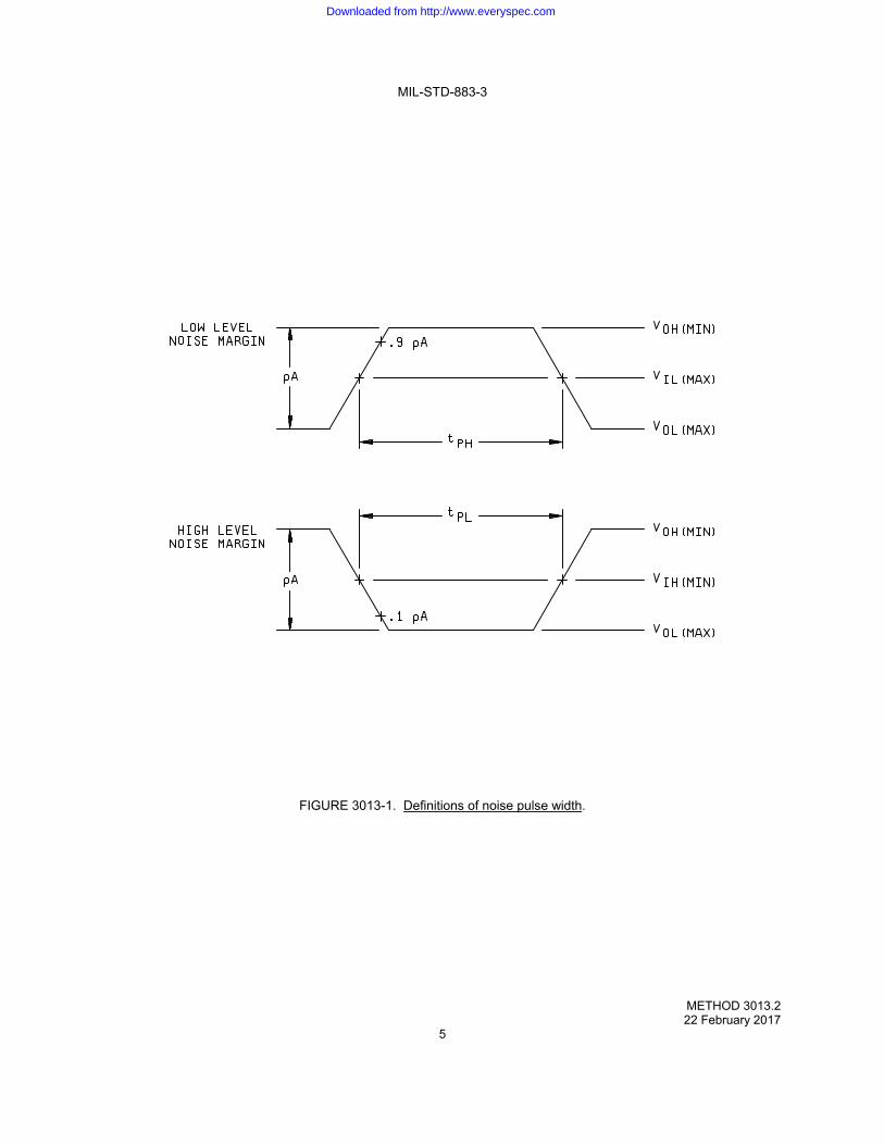
1.2.3 Noise pulse widths.
tPL: The LOW level noise pulse width, measured at the VIL (max) level.
tPH: The HIGH level noise pulse width, measured at the VIH (min) level. 2. APPARATUS. The apparatus used for noise margin measurements shall include a suitable source generator (see 2.1), load (see 2.2), and voltage detection devices for determining logic state. 2.1 Source generator. The source generator for this test shall be capable of supplying the required ac and dc noise inputs. In the case of pulsed inputs the transition times of the injected noise pulse shall each be maintained to less than 20 percent of the pulse width measured at the 50 percent amplitude level. For the purpose of this criteria, the transition times shall be between the 10 percent and 90 percent amplitude levels. The pulse repetition rate shall be sufficiently low that the element under test is at steady-state conditions prior to application of the noise pulse. For the purpose of this criteria, doubling the repetition rate or duty cycle shall not affect the outcome of the measurement. 2.2 Load. The load for this test shall simulate the circuit parameters of the normal load which would be applied in application of the device under worst-case conditions. The load shall automatically change its electrical parameters as the device under test changes logic state if this is the normal situation for the particular device load. The load shall be paralleled by a high impedance voltage detection device. 3. PROCEDURE. The device shall be connected for operation using a source generator and load as specified (see 2), and measurements shall be made of VNL, VNH, VNG, VNP, tPL, and tPH following the procedures for both ac noise margin and dc noise margin (see 3.2 through 3.3.3). 3.1 General considerations. 3.1.1 Nonpropagation of injected noise. As defined in 1.1, noise margin is the amplitude of extraneous signal which may be added to a noise-free worst case "input" level before the output breaks the allowable logic levels. This definition of noise margin allows the measurement of both dc and ac noise immunity on logic inputs or power supply lines or ground reference lines by detection of either a maximum LOW level or a minimum HIGH level at the output terminal. Since the output level never exceeds the allowable logic level under conditions of injected noise, the noise is not considered to propagate through the element under test. 3.1.2 Superposition of simultaneously injected noise. Because the logic levels are restored after one stage, and because the noise margin measurement is performed with all "inactive" inputs at the worst case logic levels, the proper system logic levels are guaranteed in the presence of simultaneous disturbances separated by at least one stage.
Downloaded from http://www.everyspec.com

MIL-STD-883-3
METHOD 3013.2 22 February 2017
3
3.1.3 Characterization of ac noise margin. Although the purpose of this standard test procedure is to insure interchangeability of elements by a single- point measurement of ac noise margin, the test procedure is well suited to the measurement of ac noise margin as a function of noise pulse width. In particular, for very wide pulse widths, the ac noise margin asymptotes to a value identically equal to the dc noise margin. 3.2 Test procedure for dc noise margin. 3.2.1 Worse case configuration. The measurement of dc noise margin using a particular logic input terminal should correspond to the worst case test configuration in the applicable acquisition document. For example, the measurement of LOW level noise margin for a positive-logic inverting NAND gate should be performed under the same worst case test conditions as the dc measurement of VOH (min). If the worst case dc test conditions for VOH (min) are high power supply voltage, all unused logic inputs connected to VOH (min) and output current equal to zero, these conditions should be applied to the corresponding dc noise margin measurement. 3.2.2 LOW level noise margin, VNL. The LOW level noise margin test is normally performed during the VOH test for inverting logic and during the VOL test for noninverting logic. The noise margin is calculated from the following expression: VNL = VIL (max) - VOL (max) 3.2.3 HIGH level noise margin, VNH. The HIGH level noise margin test is performed during the VOL test for inverting logic and during the VOH test for noninverting logic. The noise margin is calculated from the following expression: VNH = VOH (min) - VIH (min) 3.2.4 Negative ground noise margin, VNG. With all power supply and output terminals connected to the appropriate worst case conditions, apply VOL (max) to the inputs specified in the applicable acquisition document and decrease the voltage applied to the ground terminal until the output levels equal VIH (min) for inverting logic and VIL (max) for noninverting logic. The dc ground noise margin is the voltage measured at the device ground terminal. The dc source resistance of the injected ground line voltage shall be negligible. 3.2.5 Positive ground noise margin, VNG+. With all power supply and output terminals connected to the appropriate worst case conditions, apply VOH (min) to the inputs specified in the applicable acquisition document and increase the voltage applied to the ground terminal until the output levels equal VIL (max) for inverting logic and VIH (min) for noninverting logic. The dc ground noise margin is the voltage measured at the device ground terminal. The dc source resistance of the injected ground line voltage shall be negligible. 3.2.6 Power supply noise margin, VNP+ or VNP-. With all input, power supply, and output terminals connected to the appropriate worst case conditions, increase (or decrease) the power supply voltage(s) until the output level equals the appropriate logic level limit. The power supply noise margin is the difference between the measured supply voltage(s) and the appropriate noise-free worst case supply voltage level(s). If more than one power supply is required, the noise margin of each supply should be measured separately. 3.3 Test procedure for ac noise margin. 3.3.1 AC noise margin test point. If, for any combination of noise pulse width or transition times, the ac noise margin is less than the dc noise margin, the noise pulse amplitude, pulse width, and transition time which produce the minimum noise margin shall be used as the conditions for test. If the ac noise margin exceeds the dc noise margin, the dc noise margin tests only shall be performed.
Downloaded from http://www.everyspec.com

MIL-STD-883-3
METHOD 3013.2 22 February 2017
4
3.3.2 LOW level noise margin, pulse width, TPL. With all unused logic input, power supply, and output terminals connected to the appropriate worst case conditions, a positive-going noise pulse shall be applied to the input under test. The pulse amplitude shall be equal to VOH (min) minus VOL (max); the pulse amplitude shall be superimposed on a dc level equal to VOH (min); and the transition times shall be much less than the minimum transition times of the device under test. The test is performed by initially adjusting the input pulse width at the 0.9 amplitude level to one and one quarter times the rise time. The pulse width is increased until the output voltage is equal to VIH (max) for inverting logic and equal to VIL (min) for noninverting logic. The noise margin pulse width is then measured at the input pulse VIL (max) level. 3.3.3 HIGH level noise margin, pulse width, TPH. With all unused logic input, power supply, and output terminals connected to the appropriate worst case conditions, a negative-going noise pulse shall be applied to the input under test. The pulse amplitude shall be equal to VOH (min) minus VOL (max); the pulse shall be superimposed on a dc level equal to VOH (min); and the transition times shall be much less than the minimum transition times of the device under test. The test is performed by initially adjusting the input pulse width at the 0.1 amplitude level to one and one quarter times the rise time. The pulse width is increased until the output voltage is equal to VIL (min) for inverting logic and VIH (max) for noninverting logic. The noise margin pulse width is then measured at the input pulse VIH (min) level. 4. SUMMARY. The following details, when applicable, shall be specified in the applicable acquisition document:
a. VIL (max).
b. VIL (min).
c. VIH (min).
d. VIH (max).
e. VOL (max).
f. VOH (min).
g. VNL.
h. VNH.
i. VNG.
j. VNP.
k. tPL.
l. tPH.
m. Test temperature. Unless otherwise specified, dc noise margin measurements shall be made at the rated operating temperature extremes in addition to any other nominal test temperatures.
n. Specific noise margin measurements and conditions which are to be performed.
o. Power supply voltages.
p. Input conditioning voltages.
q. Output loads. r. Parameters of noise signal.
Downloaded from http://www.everyspec.com
MIL-STD-883-3
METHOD 3013.2 22 February 2017
5
FIGURE 3013-1. Definitions of noise pulse width.
Downloaded from http://www.everyspec.com

MIL-STD-883-3
METHOD 3013.2 22 February 2017
6
FIGURE 3013-2. Inverting logic gate transfer characteristic defining test points.
Downloaded from http://www.everyspec.com

MIL-STD-883-3
METHOD 3013.2 22 February 2017
7
FIGURE 3013-3. Noninverting logic gate transfer characteristic defining test points.
Downloaded from http://www.everyspec.com

MIL-STD-883-3
METHOD 3013.2 22 February 2017
8
This page intentionally left blank
Downloaded from http://www.everyspec.com

MIL-STD-883-3
METHOD 3014 15 November 1974
1
METHOD 3014 FUNCTIONAL TESTING 1. PURPOSE. This method establishes the means for assuring circuit performance in regard to the test requirements necessary to verify the specified function and to assure that all logic element paths are not open, stuck-at-HIGH level or stuck- at-LOW LEVEL. This method applies to digital microelectronic devices, such as TTL, DTL, RTL, ECL, and MOS. 2. APPARATUS. An instrument shall be provided which has the capability of applying logic patterns (sequentially, if specified) to the logic network input(s) in accordance with the applicable acquisition document. The test instrument shall also be capable of applying nominal power supply voltages and monitoring the outputs for the specified logic levels. The output monitoring circuit may be either a single or double comparator type. The threshold voltage (trip point) for a single comparator or VOL (max) and VOH (min) for a double comparator shall be specified in the applicable acquisition document. The test chamber shall be capable of maintaining the device under test at any specified test temperature. 3. PROCEDURE. The device shall be stabilized at the specified test temperature. Nominal power supply voltages and the specified input logic patterns shall be applied to the logic network under test and the output(s) monitored. 4. SUMMARY. The following details shall be specified in the applicable acquisition document:
a. Test temperature.
b. Power supply voltage.
c. Input voltage levels.
d. Input and output logic patterns.
e. Output threshold voltage (see 2).
f. VOH (min) and VOL (max) (see 2).
Downloaded from http://www.everyspec.com

MIL-STD-883-3
METHOD 3014 15 November 1974
2
This page intentionally left blank
Downloaded from http://www.everyspec.com
MIL-STD-883-3
METHOD 3015.9 7 June 2013
1
METHOD 3015.9 ELECTROSTATIC DISCHARGE SENSITIVITY CLASSIFICATION
1. PURPOSE. This method establishes the procedure for classifying microcircuits according to their susceptibility to damage or degradation by exposure to electrostatic discharge (ESD). This classification is used to specify appropriate packaging and handling requirements in accordance with MIL-PRF-38535, and to provide classification data to meet the requirements of MIL-STD-1686. 1.1 Definition. The following definition shall apply for the purposes of this test method. 1.1.1 Electrostatic discharge (ESD). A transfer of electrostatic charge between two bodies at different electrostatic potentials. 2. APPARATUS. 2.1 Test apparatus. ESD pulse simulator and device under test (DUT) socket equivalent to the circuit of figure 3015-1, and capable of supplying pulses with the characteristics required by figure 3015-2. 2.2 Measurement equipment. Equipment including an oscilloscope and current probe to verify conformance of the simulator output pulse to the requirements of figure 3015-2. 2.2.1 Oscilloscope and amplifier. The oscilloscope and amplifier combination shall have a 350 MHz minimum bandwidth and a visual writing speed of 4 cm/ns minimum. 2.2.2 Current probe. The current probe shall have a minimum bandwidth of 350 MHz (e.g., Tektronix CT-1 at 1 GHz). 2.2.3 Charging voltage probe. The charging voltage probe shall have a minimum input resistance of 1,000 MΩ and a division ratio of 4 percent maximum (e.g., HP 34111A). 2.3 Calibration. Periodic calibration shall include but not be limited to the following. 2.3.1 Charging voltage. The meter used to display the simulator charging voltage shall be calibrated to indicate the actual voltage at points C and D of figure 3015-1, over the range specified in table I. 2.3.2 Effective capacitance. Effective capacitance shall be determined by charging C1 to the specified voltage (with table I), with no device in the test socket and the test switch open, and by discharging C1 into an electrometer, coulombmeter, or calibrated capacitor connected between points A and B of figure 3015-1. The effective capacitance shall be 100 pF ±10 percent over the specified voltage range and shall be periodically verified at 1,000 volts. (Note: A series resistor may be needed to slow the discharge and obtain a valid measurement.) 2.3.3 Current waveform. The procedure of 3.2 shall be performed for each voltage step of table I. The current waveform at each step shall meet the requirements of figure 3015-2. 2.4 Qualification. Apparatus acceptance tests shall be performed on new equipment or after major repair. Testing shall include but not be limited to the following. 2.4.1 Current waveform verification. Current waveform shall be verified at every pin of each test fixture using the pin nearest terminal B (see figure 3015-1) as the reference point. All waveforms shall meet the requirements of figure 3015-2. The pin pair representing the worst case (closest to the limits) waveform shall be identified and used for the verification required by 3.2.
Downloaded from http://www.everyspec.com

MIL-STD-883-3
METHOD 3015.9 7 June 2013
2
3. PROCEDURE. 3.1 General. 3.1.1 Test circuit. Classification testing shall be performed using a test circuit equivalent to figure 3015-1 to produce the waveform shown on figure 3015-2. 3.1.2 Test temperature. Each device shall be stabilized at room temperature prior to and during testing. 3.1.3 ESD classification testing. ESD classification testing of devices shall be considered destructive. 3.2 ESD simulator current waveform verification. To ensure proper simulator operation, the current waveform verification procedure shall be done, as a minimum, at the beginning of each shift when ESD testing is performed, or prior to testing after each change of the socket/board, whichever is sooner. If the simulator does not meet all requirements, all classification testing done since the last successful verification shall be repeated. At the time of initial facility certification and recertifications, photographs shall be taken of the waveforms observed as required by 3.2c through 3.2e and be kept on file for purposes of audit and comparison. (Stored digitized representations of the waveforms are acceptable in place of photographs.)
a. With the DUT socket installed on the simulator, and with no DUT in the socket, place a short (figure 3015-1) across two pins of the DUT socket and connect one of the pins to simulator terminal A and the other pin to terminal B.
b. Connect the current probe around the short near terminal B (see figure 3015-1). Set the simulator charging
voltage source VS to 4,000 volts corresponding to step 5 of table I.
c. Initiate a simulator pulse and observe the leading edge of the current waveform. The current waveform shall meet the rise time, peak current, and ringing requirements of figure 3015-2.
d. Initiate a simulator pulse again and observe the complete current waveform. The pulse shall meet the decay
time and ringing requirement of figure 3015-2.
e. Repeat the above verification procedure using the opposite polarity (VS = -4,000 volts).
f. It is recommended that the simulator output be checked to verify that there is only one pulse per initiation,
and that there is no pulse while capacitor C1 is being charged. To observe the recharge transient, set the trigger to the opposite polarity, increase the vertical sensitivity by approximately a factor of 10, and initiate a pulse.
Downloaded from http://www.everyspec.com

MIL-STD-883-3
METHOD 3015.9 7 June 2013
3
TABLE I. Simulator charging voltage (VS) steps versus peak current (IP). 1/
Step VS (volts) IP (amperes)
1 250 0.17
2 500 0.33
3 1,000 0.67
4 2,000 1.33
5 4,000 2.67
1/ IP is the current flowing through R2 during the current waveform verification procedure and which is approximately VS/1,500 ohms. 3.3 Classification testing.
a. A sample of devices (see 4.c) shall be characterized for the device ESD failure threshold using the voltage
steps shown in table I, as a minimum. Finer voltage steps may optionally be used to obtain a more accurate measure of the failure voltage. Testing may begin at any voltage step, except for devices which have demonstrated healing effects, including those with spark gap protection, which shall be started at the lowest step. Examination of known technology family input or output V/I damage characteristics (i.e., curve tracer), or other simplified test verification techniques may be used to validate the failure threshold (e.g., cumulative damage effects may be eliminated by retesting at the failure voltage step using a new sample of devices and possibly passing the step).
b. A new sample of devices shall be selected and subjected to the next lower voltage step used. Each device
shall be tested using three positive and three negative pulses using each of the pin combinations shown in table II. A minimum of 1 second delay shall separate the pulses.
c. The sample devices shall be electrically tested to subgroups 1 and 7 as applicable (room temperature dc
parameters and functional tests).
d. If one or more of the devices fail, the testing of 3.3b and 3.3c shall be repeated at the next lower voltage step used.
e. If none of the devices fail, record the failure threshold determined in 3.3a. Note the highest step passed,
and use it to classify the device according to table III.
Downloaded from http://www.everyspec.com

MIL-STD-883-3
METHOD 3015.9 7 June 2013
4
TABLE II. Pin combinations to be tested. 1/ 2/
Terminal A (Each pin individually connected to terminal A with the other floating)
Terminal B (The common combination of all like-named pins connected to terminal B)
1. All pins except Vps1 3/ All Vps1 pins
2. All input and output pins All other input-output pins
1/ Table II is restated in narrative form in 3.4 below. 2/ No connects are not to be tested. 3/ Repeat pin combination 1 for each named power supply and for ground (e.g., where Vps1 is VDD, VCC, VSS, VBB, GND, +VS, -VS, VREF, etc.) 3.4 Pin combination to be tested.
a. Each pin individually connected to terminal A with respect to the device ground pin(s) connected to terminal B. All pins except the one being tested and the ground pin(s) shall be open.
b. Each pin individually connected to terminal A with respect to each different set of a combination of all named
power supply pins (e.g., VSS1 or VSS2 or VSS3 or VCC1 or VCC2) connected to terminal B. All pins except the one being tested and the power supply pin or set of pins shall be open.
c. Each input and each output individually connected to terminal A with respect to a combination of all the other
input and output pins connected to terminal B. All pins except the input or output pin being tested and the combination of all the other input and output pins shall be open.
Note: As an option, a shunt resistance of 10k ohms or higher may be used to ease the pre-pulse voltage
phenomenon that occurs, especially in high-impedance pins. The shunt resistance will be placed between the pin to be stressed (Terminal A) and the system ground (Terminal B) and as long as it does not alter the Human Body Model (HBM) waveform specifications or the tester qualification, calibration and waveform verification. The shunt resistance can be placed in the HBM simulator or in the test fixturing system.
Downloaded from http://www.everyspec.com
MIL-STD-883-3
METHOD 3015.9 7 June 2013
5
TABLE III. Device ESD failure threshold classification. 4. SUMMARY. The following details shall be specified in the applicable purchase order or contract, if other than specified herein.
a. Post test electricals. b. Special additional or substitute pin combinations, if applicable.
c. Sample size, if other than three devices.
Class 0 < 250 volts
Class 1A 250 volts to 499 volts
Class 1B 500 volts to 999 volts
Class 1C 1,000 volts to 1,999 volts
Class 2 2,000 volts to 3,999 volts
Class 3A 4,000 volts to 7,999 volts
Class 3B > 8,000 volts
Downloaded from http://www.everyspec.com

MIL-STD-883-3
METHOD 3015.9 7 June 2013
6
R1 = 106 ohms to 107 ohms C1 = 100 picofarads ±10 percent (Insulation resistance 1012 ohms minimum) R2 = 1,500 ohms ±1 percent S1 = High voltage relay (Bounceless, mercury wetted, or equivalent) S2 = Normally closed switch (Open during discharge pulse and capacitance measurement) NOTES:
1. The performance of this simulator circuit is strongly influenced by parasitics. Capacitances across relays and
resistor terminals, and series inductance in wiring and in all components shall be minimized. 2. As a precaution against transients upon recharge of C1, the supply voltage VS may be reduced before
switch S1 is returned to the charging position. 3. Piggybacking DUT sockets is not permitted during verification or classification testing. 4. Switching terminals A and B internal to the simulator to obtain opposite polarity is not allowed. 5. C1 represents the effective capacitance (see 2.3.2). 6. The current probe connection shall be made with double shielded cable into a 50-ohm termination at the
oscilloscope. The cable length shall not exceed 3 feet.
FIGURE 3015-1. ESD classification test circuit (human body model).
Downloaded from http://www.everyspec.com

MIL-STD-883-3
METHOD 3015.9 7 June 2013
7
NOTES:
1. The current waveforms shown shall be measured as described in the waveform verification procedure of 3.2, using equipment meeting the requirements of 2.
2. The current pulse shall have the following characteristics: Tri (rise time) ------------- Less than 10 nanoseconds. Tdi (delay time) ---------- 150 ±20 nanoseconds. Ip (peak current) ---------- Within ±10 percent of the Ip value shown in table II for the voltage step selected. Ir (ringing) ------------------ The decay shall be smooth, with ringing, break points, double time constants or discontinuities less than 15 percent Ip maximum, but not observable 100 nanoseconds after start of the pulse. FIGURE 3015-2. ESD classification test circuit waveforms (human body model).
Downloaded from http://www.everyspec.com

Downloaded from http://www.everyspec.com

MIL-STD-883-3
METHOD 3016.1 7 June 2013
1
METHOD 3016.1 ACTIVATION TIME VERIFICATION 1. PURPOSE. This method establishes a means for assuring circuit performance during cold temperature start up. It defines an activation time for digital microelectronic devices such as TTL, DTL, RTL, ECL, and MOS and establishes the procedure necessary to accomplish the required testing. This method will ensure that a specified capability is available a known time interval after application of power. 1.1 Definitions. The following definitions shall apply for the purposes of this test method:
a. Activation time. Activation time is defined as the time required for a device to become functionally operable after initial power is applied at the operating temperature extremes as specified by the applicable acquisition document. Note that activation time may be due to device and test system limitations, or both.
b. Maximum and minimum. Maximum and minimum refer to an algebraic system where "max" represents the
most positive value of the range and "min" represents the least positive value of the range. This is consistent with MIL-HDBK-1331, 30.1 and 30.2 for logic levels only.
c. Maximum operating frequency. Maximum operating frequency is defined as the frequency of operation
resulting from use of the minimum clock period for devices requiring a clock, or the frequency of operation resulting from the use of the minimum cycle time for devices not requiring a clock (such as memory devices) as specified in the applicable acquisition document.
1.2 Symbols. The following symbols and definitions shall apply for the purposes of this method. 1.2.1 Logic levels.
a. VLW = worst case nominal low level logic input. The maximum allowable VIL specified in the applicable acquisition document minus 100 millivolts to allow for uncertainty in the drive level capability of high speed functional test equipment. (VLW = VIL (max) - 100 mV).
b. VHW = worst case nominal high level logic input. The minimum allowable VIH as specified by the applicable
acquisition document plus 100 millivolts (VHW = VIH (min) + 100 mV).
c. VOH (min) = minimum output high level specified for a digital microelectronic device.
d. VOL (max) = maximum output low level specified for a digital microelectronic device. 1.2.2 Activation times.
a. tAH = maximum allowable activation time requirement, measured at VCC (max). b. tAL = maximum allowable activation time requirement, measured at VCC (min).
2. APPARATUS. An instrument shall be provided which has the capability of applying sequential logic patterns to the device under test in accordance with the applicable acquisition document. The test instrument shall also be capable of applying nominal power supply voltage(s) and monitoring the output for the specified logic levels. The output monitoring circuit shall be of the double comparator type. The threshold voltage (trip point) for a comparator shall be VOL (max) and VOH (min) as specified in the applicable acquisition document. The test chamber shall be capable of maintaining the device under test at any specified test temperature.
Downloaded from http://www.everyspec.com

MIL-STD-883-3
METHOD 3016.1 7 June 2013
2
3. PROCEDURE. The device shall be thermally stabilized at the minimum specified test temperature with no power applied to the device. The specified power supply voltage and the specified input logic patterns using VLW and VHW input voltage levels shall then be applied to the device under test and the outputs shall be monitored as described in section 2. This functional test shall be performed at a speed of at least 75 percent of F(max) using a test vector pattern as called out in the applicable acquisition document that has been designed for maximum fault coverage with no more than 4 K vectors. 3.1 Activation time, maximum supply voltage, tAH. Available test equipment has inherent delays (due to test program statement execution, voltage driver rise/fall times, etc.) between the time power is applied to the device under test and actual execution of the test. Therefore, the activation time stated in the applicable acquisition document should not be specified as less than the test system delay (even though device performance may be better). The test sequence shall be as follows. 3.1.1 Device under test. The device under test shall be thermally stabilized at the minimum specified test temperature, with the device unpowered. 3.1.2 Device under test shall then be powered up at VCC (max). After waiting the time specified by TAH (taking into account test equipment delays), the functional test pattern (using VLW and VHW) logic levels) shall be applied to verify proper operation. 3.1.3 Repeat sequences 3.1.1 and 3.1.2 at the maximum specified test temperature. 3.2 Activation time, minimum supply voltage, tAL. Repeat sequence described in 3.1.1 to 3.1.3 using a supply voltage of VCC (min). 3.3 Failure criteria. The device must pass the functional test pattern and is a failure if the device fails any single pattern or vector in the specified test set. 4. SUMMARY. The following details, when applicable, shall be as specified in the applicable acquisition document:
a. VIL (max).
b. VIH (min).
c. VOH (min).
d. VOL (max).
e. VCC (min).
f. VCC (max).
g. Test temperature (min and max operating temperature).
h. tAH (max).
i. tAL (max). j. Functional test pattern (see 3).
k. Maximum operating frequency, F (max) (see 1.1.c).
Downloaded from http://www.everyspec.com

MIL-STD-883-3
METHOD 3017 29 May 1987
1
METHOD 3017 MICROELECTRONICS PACKAGE DIGITAL SIGNAL TRANSMISSION 1. PURPOSE. This method establishes the means of evaluating the characteristic impedance, capacitance, and delay time of signal lines in packages used for high frequency digital integrated circuits. It is intended to assure a match between circuit performance and interconnecting wiring to minimize signal degradation. 1.1 Definitions. 1.1.1 Characteristic impedance. The impedance that a section of transmission line exhibits due to its ratio of resistance and inductance to capacitance. 1.1.2 Delay time. The time delay experienced when a pulse generated by a driver with a particular drive impedance is propagated through a section of transmission line. 1.2 Symbols. R: Resistance L: Inductance C: Capacitance tpd: Propagation delay time 2. APPARATUS. The approaches for transmission performance measurements shall include a suitable time domain reflectometer (TDR) (see 2.1) and dc resistance measuring equipment (see 2.2). 2.1 Time domain reflectometer. The TDR used for this test shall have a system rise time for the displayed reflection that is not less than 5 times and preferably 10 times the rise time (method 3004) for the candidate integrated circuits to be packaged. Interconnecting cables and fixtures shall be designed such that this ratio is not degraded due to reflections and ringing in the test setup. 2.2 DC resistance. DC resistance measuring equipment and probe fixtures shall be capable of measuring the resistance of the package leads and the chip-to- package interconnect media with an accuracy of no greater than ±10 percent of the actual value including errors due to the mechanical probing interface contact resistance. 3. PROCEDURE. The test equipment configuration shall be as shown on figure 3017-1 using a time domain reflectometer as specified (see 2). The characteristic impedance (Zo), propagation time (tpd), resistance and load capacitance (CL) shall be measured for all representative configurations as determined by a review of the package drawings, and the intended applications (see 3.2 through 3.3). 3.1 General considerations. 3.1.1 TDR measurements. Accurate measurement of transmission performance of a package pin using a TDR requires careful design and implementation of adapter fixtures to avoid reflections due to transmission line discontinuities in the cables and junctions between the TDR and the package being tested. The accuracy of the measurement will be enhanced if the coaxial cable used to interface to the package is of a characteristic impedance as close as possible to the package pin impedance. The interface to the package should be a soldered connection and mechanical design of the actual coax-to-package interface should minimize the length of the uncontrolled impedance section. Stripline interfaces are the best method for surface mount package styles.
Downloaded from http://www.everyspec.com

MIL-STD-883-3
METHOD 3017 29 May 1987
2
3.1.2 Test configurations. Obtaining a good high frequency ground is also important. Connection of the package ground plane (if the package design has one) to the test set-up ground plane should be accomplished with a pin configuration similar to actual usage in the intended package applications. Pin selection for testing may vary according to package complexity. For packages with very symmetrical pin configurations only a few pins need be tested but configurations must include pins adjacent and nonadjacent to the ground pins. Packages with complex wiring and interconnection media should be tested 100 percent. 3.2 Test procedure for package transmission characteristics. Using a section of coaxial cable of known, calibrated characteristic impedance (ZRef) as a reference measure the minimum (ZMin) maximum (ZMax) and average (Zo) values of reflection coefficient () for the section of line on the TDR display that has been carefully determined to be the package pin (locate using zero-length short circuits). 3.2.1 Characteristic impedance. Calculate characteristic impedance (Zo) for each of the cases from the formula:
0 RefZ = Z x (1+ )
(1 - )
3.2.2 Delay time measurement. From the TDR display of 3.2.1 measure the time difference in picoseconds from the point identified as the start of the exterior package pin (t1) to the chip interface point (t2) (t = t1-t2) Form the package design drawings, determine the physical length of the package run (L)
Time delay t = t
Lpd
3.2.3 Load capacitance calculation.
Load capacitance C = t
ZL
pd
o
3.2.4 Load inductance calculation.
Load inductance (series) = ( t )
Cpd
2
L
3.3. Series resistance measurement. Using the test setups of figure 3017-2, separately measure the dc resistance of the chip-to-package interface media (RM) and the package lead (RL).
Downloaded from http://www.everyspec.com

MIL-STD-883-3
METHOD 3017 29 May 1987
3
4. SUMMARY. The following details, when applicable, shall be specified in the applicable acquisition document:
a. ZMax.
b. ZMin.
c. Zo (max).
d. Zo (min).
e. tpd (max).
f. tpd (min).
g. CL (max).
h. CL (min).
i. LL (max).
j. LL (min).
k. RM (max).
l. RM (min).
m. RL (max).
n. RL (min).
o. Package pins to be tested.
p. Package ground configuration.
Downloaded from http://www.everyspec.com

MIL-STD-883-3
METHOD 3017 29 May 1987
4
FIGURE 3017-1. Time domain reflectometer test setup.
Downloaded from http://www.everyspec.com
MIL-STD-883-3
METHOD 3017 29 May 1987
5
FIGURE 3017-2. Test setup for dc resistance using a milliohmmeter.
Downloaded from http://www.everyspec.com

MIL-STD-883-3
METHOD 3017 29 May 1987
6
This page intentionally left blank
Downloaded from http://www.everyspec.com

MIL-STD-883-3
METHOD 3018 29 May 1987
1
METHOD 3018 CROSSTALK MEASUREMENTS FOR DIGITAL MICROELECTRONICS DEVICE PACKAGE 1. PURPOSE. This method establishes the means of measuring the level of cross-coupling of wideband digital signals and noise between pins in a digital microcircuit package. The method may be used to gather data that are useful in the prediction of the package's contribution to the noise margin of a digital device. The technique is compatible with multiple logic families provided that the drive and load impedance are known. 1.1 Definitions. 1.1.1 Crosstalk. Signal and noise waveforms coupled between isolated transmission lines, in this case, package conductors. 1.1.2 Coupling capacitance. The effective capacitance coupling between a pair of conductors in a package as measured by the time constant of the charge pulse applied on one line and measured on the other. 1.1.3 Noise pulse voltage. The voltage of a crosstalk measured at the minimum noise pulse width as measured on a receiver input line. 1.1.4 Peak noise voltage. The peak value of the noise pulse measured on a receiver input line. 1.2 Symbols. The following symbols shall apply for the purpose of this test method and shall be used in accordance with the definitions provided (see 1.2.1 and 1.2.2). 1.2.1 Logic levels. VOL(max): The maximum output low level specified in a logic system. VOH(min): The minimum output high level specified in a logic system. VIL(max): The maximum allowed input low voltage level in a logic system. VIH(min): The minimum allowed input high level in a logic system. 1.2.2 Noise pulse width. tPL: The low level noise pulse width, measured at the VIL (max) level (see method 3013). tPH: The high level noise pulse width, measured at the VIH (min) level (see method 3012). 1.2.3 Transition times (see method 3004). ttLH: Rise time. The transition time of the output from the 10 percent to the 90 percent of the high voltage
levels with the output changing from low to high. ttHL: Fall time. The transition times from the 90 percent to the 10 percent of the high voltage level with the
output changing from high to low. 1.2.4 Crosstalk parameters. Cc: Coupling capacitance (see 1.1.2). VN: Noise pulse voltage (see 1.1.3). VNPK: Peak noise voltage (see 1.1.4).
Downloaded from http://www.everyspec.com
MIL-STD-883-3
METHOD 3018 29 May 1987
2
2. APPARATUS. The apparatus used for crosstalk measurements shall include a suitable source generator (see 2.1), wideband oscilloscope (see 2.2), low capacitance probe (see 2.3) and load resistors (see 2.4). 2.1 Source generator. The source generator for this test shall be capable of duplicating (within 5 percent) the transition times, VOH and VOL levels of the logic system(s) being considered for application using the package style under evaluation. The source generator shall have a nominal characteristic source impedance of 50 Ω. 2.2 Wideband oscilloscope. The oscilloscope used to measure the crosstalk pulse shall have a display risetime that is less than 20 percent of the risetime of the logic systems being considered for application in the package style under evaluation. A sampling-type oscilloscope is recommended. 2.3 Low capacitance probe. The interface between the oscilloscope and the unit under test shall be a high impedance low capacitance probe. The probe impedance shall be 10 kΩ, minimum and the capacitance shall be 5 pF, maximum, unless otherwise specified in the acquisition document. 2.4 Load resistor. The load resistors specified for this test shall be low inductance, low capacitance, chip style resistors with a tolerance of ±5 percent. Load resistor values(s) shall be specified by the acquisition document to match the load impedance levels of the application logic family for a single receiver load. 3. PROCEDURE. The test equipment configuration shall be as shown on figure 3018-1 using a source generator, oscilloscope, probe and loads as specified (see 2). Measurements shall be made of coupling capacitance, (see 3.2) and if required by the acquisition document, of noise pulse voltage, peak noise pulse voltage, and noise pulse width (see 3.3). 3.1 General considerations. 3.1.1 Package test configuration. It is important to ground the package using the same pins as would be used in the microcircuit application. If the package has an internal ground plane or ground section, this should be connected via package pin(s) to the exterior test set-up ground plane. The package should be connected to the test set-up with coaxial cable or stripline. Unshielded conductor medium should not be used between the signal source and package. Coaxial shields must be grounded at both ends of the cable. Package sockets should not be used unless these are to be part of the microcircuit application configuration. Package leads must be formed and trimmed as specified in the application. Package-to-chip interconnecting media shall be installed in the package and used to connect to the load resistors. 3.1.2 Pin selection. For simple packages with symmetrical, parallel pin conductors, only a sample of pin combinations need be tested. Unless otherwise specified by the acquisition document, all combinations adjacent to the ground pin(s) and combinations opposite the ground pin(s) shall be tested, as a minimum. Complex packages with nonparallel conductors or multilayer wiring shall be tested for all adjacent-pair combinations, unless otherwise specified. 3.2 Coupling capacitance measurements. Connect the test equipment as shown on figure 3018-1. Use a 50 Ω chip resistor load in the driven pin channel, unless otherwise specified. For the pick-up channel, use the load resistor value(s) as specified by the acquisition document. (Load resistor values should be set such that the parallel combination of load resistance and probe impedance matches as closely as practical the specified load impedance of a single receiver in the logic system to be used in the microcircuit application.) Check the residual cross-coupling of the measuring set-up by touching the probe to the pick-up channel load before the pick-up pin is connected to the resistor. Measure and record the peak pulse voltage observed. This peak pulse reading must be less than 50 percent of the reading observed with the pin connected to the resistor for a reading to be valid. Adjust the test set-up cable orientation and configuration to minimize this residual cross-coupling.
Downloaded from http://www.everyspec.com

MIL-STD-883-3
METHOD 3018 29 May 1987
3
Connect the pick-up pins to the load resistor and adjust the pulse width so that the time required to charge the coupling capacitance to 0 V can be observed. Measure the time at the 63 percent voltage point on the waveform (T) and calculate coupling capacitance (Cc) as follows:
Determine R = R x R
R + RTotal
Probe Load
Probe Load
TotalTotal
C = T
R
C Total ProbeC = C - C Values of CC can be used as a relative measure for comparison of potential crosstalk among several packages to a standard package. The coupling capacitance (C c) can also be used to predict levels of crosstalk for various logic systems or circuit configurations by performing a pulse response analysis using a circuit simulator. 3.3 Noise pulse measurements. Using the same test setup as in 3.2, measure the crosstalk noise pulse voltage at the minimum noise pulse width specified for the logic system or as specified by the acquiring agency. Measure the peak noise voltage value of the coupled crosstalk. 4. SUMMARY. The following details, when applicable, shall be specified in the acquisition document:
a. Cc.
b. VOL (max).
c. VOH (min).
d. VIL (max). e. VIH (min).
f. tPL.
g. tPH.
h. ttLH.
i. ttHL.
j. VN.
k. VNPK.
Downloaded from http://www.everyspec.com

MIL-STD-883-3
METHOD 3018 29 May 1987
4
FIGURE 3018-1. Test setup for coupling capacitance measurement.
Downloaded from http://www.everyspec.com

MIL-STD-883-3
METHOD 3019.2 22 February 2017
1
METHOD 3019.2 GROUND AND POWER SUPPLY IMPEDANCE MEASUREMENTS FOR MICROELECTRONICS DEVICE PACKAGE 1. PURPOSE. This method establishes the means of measuring the series impedance of the ground and power supply circuit pin configurations for packages used for complex, wide bandwidth microcircuits. The method provides data that are useful in the evaluation of the relative performance of various packages and can be used to predict the contribution of the package to power supply noise and ground noise. 1.1 Definition. 1.1.1 Ground or power supply impedance. The series combination of inductive reactance and resistance exhibited by all of the conductor paths between the semiconductor chip interface and the exterior package interface in either the ground circuit or the power supply circuit. The impedance of a series inductive circuit is defined by the equation:
Z = R + X L2 2 1.2 Symbols. The following symbols shall apply for purposes of this test method and shall be used in conjunction with the definition provided in 1.1. LG: Series inductance of the ground circuit path in a package (henries). Lp: Series inductance of the power supply circuit path in a package (henries). XG: Series inductive reactance of ground path = 2 π fLG (ohms). Xp: Series inductive reactance of power supply path = 2 π fLp (ohms). f: Frequency (Hz). ftr: Frequency of primary component of digital pulse transition = 1 (Hz). tt ftp: Frequency related to noise pulse width specified for the logic system:
tp
(Hz)
Pmin
f = 1
t
tt: Transition time from logic system. Equal to the smaller value of low to high or high to low transition. ZG: Series impedance of ground path at frequency:
G2
G2
GZ = R + Z
Zp: Series impedance of power supply path at frequency:
p2
p2
pZ = R + Z
tPmin: The minimum noise pulse width at either the VIH or VIL level specified for a given logic system.
Downloaded from http://www.everyspec.com

MIL-STD-883-3
METHOD 3019.2 22 February 2017
2
2. APPARATUS. The apparatus used for ground impedance measurements shall include a suitable RF inductance meter and a suitable milliohmmeter. 2.1 RF inductance meter. The RF inductance meter (or multi-frequency LCR meter) shall be capable of ac measurements of series inductance over the range of 1 nH to 1,000 nH at a frequency of 100 kHz with an accuracy of ±5 percent including test fixture errors. 2.2 Milliohmmeter. The milliohmmeter (or LCR meter) shall be capable of measuring resistance using a 4-wire method over the range from 10 M to 10 with an accuracy of ±5 percent, including test fixture errors.
Downloaded from http://www.everyspec.com

MIL-STD-883-3
METHOD 3019.2 22 February 2017
3
3. PROCEDURE. Measurement of series ground impedance (ZG) and power supply impedance (Zp) shall be made for all standard power and ground configurations specified for the package application. Measurements shall be performed in accordance with 3.2. 3.1 General considerations. Accurate measurement of series impedance requires careful design and implementation of test adapters to minimize errors. Since the inductance and resistance values being measured are usually quite small, means must be provided to null out the tare resistance and inductance of the test adapters through 4-wire methods and substraction techniques. The tare values of the interconnecting circuits must be small to enable the meters to read on ranges that provide adequate resolution and accuracy. The techniques specified herein are adequate for predicting impedance at frequencies up to 1 GHz. Impedance shall be evaluated at a frequency related to either the transition time:
trtr
f = 1
t
or to the noise pulse width of the logic system used in the package:
tpPmin
f = 1
t
The frequency f shall be as specified in the acquisition document. The configuration of the package being tested must be the same as in the application. Wirebonds and other interconnection media must be included in the measurement. The package should be mounted on a dielectric holding fixture to avoid stray capacitance between the package and test equipment ground planes. Sockets should not be used unless specified. Package leads must be trimmed to applications specifications. 3.2 Test procedure for series impedance. 3.2.1 Series inductance. With the inductance meter, measure the series inductance of the power supply circuit (Lp) between the external package solder interface and the chip power supply location. Similarly, measure the inductance of the ground circuit (LG). Calculate Xp = 2 π fLp and XG = 2 π fLG. 3.2.2 Series resistance. With the milliohmmeter, measure the series resistance of the same power and ground circuits: RP and RG. 3.2.3 Calculation of impedance.
Calculate Z = X + Rp p2 2
p
G2
G2
GA = X + R
Downloaded from http://www.everyspec.com

MIL-STD-883-3
METHOD 3019.2 22 February 2017
4
4. SUMMARY. The following details, when applicable, shall be specified in the applicable acquisition document.
a. Zp (max).
b. ZG (max).
c. LP (max).
d. LG (max).
e. RP (max).
f. RG (max).
g. f.
h. ftr.
i. ftp.
j. tt.
k. tPmin.
Downloaded from http://www.everyspec.com
MIL-STD-883-3
METHOD 3020 29 May 1987
1
METHOD 3020 HIGH IMPEDANCE (OFF-STATE) LOW-LEVEL OUTPUT LEAKAGE CURRENT 1. PURPOSE. This method establishes the means for assuring circuit performance to the limits specified in the applicable acquisition document in regard to output leakage current when an output is in the high-impedance state with a low-level voltage applied. This current should normally be specified as a maximum negative value (IOLZ maximum). This method applies to digital microelectronic devices, such as TTL, DTL, RTL, ECL, and MOS that have tristate outputs. 2. APPARATUS. The test chamber shall be capable of maintaining the device under test at any specified test temperature. An instrument shall be provided that has the capability of applying the specified low level voltage to the output terminal and measure the resultant current flowing in the terminals. 3. PROCEDURE. The device shall be stabilized at the specified test temperature. Apply voltages to the test circuit as follows:
a. Worst-case power supply voltage (VCC) applied to the VCC terminal.
b. Threshold-level voltages (VIH minimum or VIL maximum) applied to the control inputs which forces the output under test into the high-impedance (off) state.
c. Nonthreshold level voltage applied to the logic input terminals controlling the output under test so as to
produce a "hard" high voltage level at that output if the output was not in the high-impedance state. Apply the specified low logic level voltage to the output terminal under test and measure the resultant leakage current. Outputs shall be measured individually.
4. SUMMARY. The following details shall be specified in the applicable acquisition document:
a. Test temperature.
b. Worst case power supply voltages.
c. Threshold voltage levels for control inputs.
d. Voltages at logic input terminals for output under test.
e. Output voltage.
f. IOLZ maximum negative limit.
Downloaded from http://www.everyspec.com

MIL-STD-883-3
METHOD 3020 29 May 1987
2
This page intentionally left blank
Downloaded from http://www.everyspec.com

MIL-STD-883-3
METHOD 3021 29 May 1987
1
METHOD 3021 HIGH IMPEDANCE (OFF-STATE) HIGH-LEVEL OUTPUT LEAKAGE CURRENT 1. PURPOSE. This method establishes the means for assuring circuit performance to the limits specified in the applicable acquisition document in regard to output leakage current when an output is in the high-impedance state with a high-level voltage applied. This current should normally be specified as a maximum positive value (IOHZ maximum). This method applies to digital microelectronic devices, such as TTL, DTL, RTL, ECL and MOS that have tristate outputs. 2. APPARATUS. The test chamber shall be capable of maintaining the device under test at any specified test temperature. An instrument shall be provided that has the capability of applying the specified high level voltage to the output terminal and measure the resultant current flowing out of the terminals. 3. PROCEDURE. The device shall be stabilized at the specified test temperature. Apply voltages to the test circuit as follows:
a. Worst-case power supply voltage (VCC) applied to the VCC terminal.
b. Threshold level voltage (VIH minimum or VIL maximum) applied to the control inputs which will cause the output under test to be in the high-impedance (off) state.
c. Nonthreshold level voltage applied to the logic input terminals controlling the output under test so as to
produce a "hard" low voltage level at that output if the output was not in the high-impedance state. Apply the specified high logic level voltage to the output terminal under test and measure the resultant leakage current. Outputs shall be measured individually.
4. SUMMARY. The following details shall be specified in the applicable acquisition document:
a. Test temperature.
b. Worst case power supply voltages.
c. Threshold voltage levels for control inputs.
d. Voltages at logic input terminals for output under test. e. Output voltage.
f. IOLZ maximum positive limit.
Downloaded from http://www.everyspec.com
MIL-STD-883-3
METHOD 3021 29 May 1987
2
This page intentionally left blank
Downloaded from http://www.everyspec.com

MIL-STD-883-3
METHOD 3022 29 May 1987
1
METHOD 3022 INPUT CLAMP VOLTAGE 1. PURPOSE. This method establishes the means for assuring circuit performance to the limits specified in the applicable acquisition document in regard to input voltage levels in a region of relatively low differential resistance that serve to limit the input voltage swing. Input clamp voltage is specified as a maximum positive value (VIC POS) or the maximum negative value (VIC NEG). This method applies to digital microelectronic devices. 2. APPARATUS. The test chamber shall be capable of maintaining the device under test at any specified test temperature. The test apparatus shall be capable of supplying the worst case power supply voltage and shall be capable of loading the input of the circuit under test with the specified negative current or the specified positive current, both referred to as IIN. Resistors may be used to simulate the applicable current levels. 3. PROCEDURE. The device shall be stabilized at the specified test temperature. Apply worst-case power supply voltage (VCC) to the VCC terminal. Force the specified negative current from or the positive current into the input under test and measure the resultant input voltage. (NOTE: Any input for which the IIL would influence the negative input current (IIN) should have VIC measured with the VCC terminal open). All input terminals not under test may be high, low, or open to minimize or inhibit any outside factors (noise, transients, etc.) from affecting the test. Inputs shall be tested individually. 4. SUMMARY. The following details shall be specified in the applicable acquisition document:
a. Test temperature.
b. Worst case power supply voltage.
c. Current to be forced from the input terminal.
d. VIC (POS) or VIC (NEG) maximum limit.
Downloaded from http://www.everyspec.com

MIL-STD-883-3
METHOD 3022 29 May 1987
2
This page intentionally left blank
Downloaded from http://www.everyspec.com

MIL-STD-883-3
METHOD 3023.2 7 June 2013
1
METHOD 3023.2
STATIC LATCH-UP MEASUREMENTS FOR DIGITAL CMOS MICROELECTRONIC DEVICES
Latchup shall be performed in accordance with JEDEC JESD78. JEDEC JESD78 supersedes JEDEC-STD-17.
Downloaded from http://www.everyspec.com

MIL-STD-883-3
METHOD 3023.2 7 June 2013
2
This page intentionally left blank
Downloaded from http://www.everyspec.com

MIL-STD-883-3
METHOD 3024 19 August 1994
1
METHOD 3024
SIMULTANEOUS SWITCHING NOISE MEASUREMENTS FOR DIGITAL MICROELECTRONIC DEVICES
1. Purpose. This method establishes the procedure for measuring the ground bounce (and VCC bounce) noise in digital microelectronic devices or to determine compliance with specified ground bounce noise requirements in the applicable acquisition document. It is also intended to provide assurance of interchangeability of devices and to eliminate misunderstanding between manufacturers and users on ground bounce noise test procedures and requirements. This procedure is not intended to predict the amount of noise generated on an end product board, but for use in measuring ground bounce noise using a standardized method for comparing noise levels between logic families and vendors. 1.1 Definitions. The following definitions shall apply for the purposes of this test method:
a. Ground bounce noise. The voltage amplitude (peak) of extraneous signals present on a low-level non-switching output with a specified number of other outputs switching. Ground bounce noise on a logic low output can be of sufficient amplitude to exceed the high level threshold of a receiver, or cause latch-up on unprotected CMOS inputs.
b. VCC bounce noise. The voltage amplitude (peak) of extraneous signals present on a high-level non-
switching output with a specified number of other outputs switching. VCC bounce on a logic high output can be of sufficient amplitude to exceed the low level threshold of a receiver, or cause latch-up on unprotected CMOS inputs.
c. Simultaneous switching noise. Noise generated across the inductance of a package pin as a result of the
charge and discharge of load capacitance through two or more transitioning output pins.
d. Quiet low. A non-switching output which is driving a nominal low level.
e. Quiet high. A non-switching output which is driving a nominal high level.
f. Signal skew. The amount of time measured between any two signal transitions at the 1.5 V voltage level (for TTL threshold devices) and at VCC/2 (for CMOS threshold devices).
1.2 Symbols. The following symbols shall apply for the purposes of this test method: 1.2.1 Logic levels.
VIL max: The maximum allowed input low level on a digital microelectronic device.
VIL min: The minimum allowed input low level on a digital microelectronic device.
VIH max: The maximum allowed input high level on a digital microelectronic device.
VIH min: The minimum allowed input high level on a digital microelectronic device.
Downloaded from http://www.everyspec.com

MIL-STD-883-3
METHOD 3024 19 August 1994
2
1.2.2 Noise levels.
VOLP max: The largest positive amplitude transient allowed on a logic low output.
VOLV max: The largest negative amplitude transient allowed on a logic low output.
VOHP max: The largest positive amplitude transient allowed on a logic high output.
VOHV max: The largest negative amplitude transient allowed on a logic high output. 1.2.3 Transition times.
TTLH: The transition time of a rising edge (rise time) measured from 10 percent to 90 percent.
TTHL: The transition time of a rising edge (fall time) measured from 90 percent to 10 percent. 2. Apparatus. The apparatus used for ground bounce noise measurements shall include a suitable source generator (see 2.1), loads (see 2.2), an oscilloscope (see 2.3) and a low noise test fixture (see 2.4). See figure 3024-1 for proper connections. 2.1 Source generator. The pulse or pattern generator for this test shall be capable of supplying the required input pulses with transition times of 3.0 0.5 ns to minimize skew due to input threshold differences. 2.2 Loads. Loads shall consist of 50 pF capacitance (-0,+20%) and a 500 ohm (1%) low inductance resistor from each output to ground. Capacitance value should include probe and test fixture capacitance. The 500 ohm resistor may be made up of a 450 ohm resistor in series with a 50 ohm oscilloscope input channel or 50 ohm termination. 2.3 Oscilloscope. The oscilloscope and probe combination shall have a minimum bandwidth of 1 GHz. Probes (if used) must be calibrated using the manufacturers instructions before accurate measurements can be made. 2.4 Test fixture. Test fixture construction has a large impact on the accuracy of the results. Therefore, the standard ESH test fixture or an equivalent approved fixture (one which demonstrates results within 10% of the standard) must be used to perform these tests. (The ESH fixture for DIP devices is LAB-350-28. Other standard fixtures will be determined at a later date.) Lead lengths should be 0.25 inches or less. The devices under test may be clamped to the test fixture, soldered to the fixture, or installed in a socket on the fixture. Use of a socket may result in higher readings. 3. Procedure. The device shall be installed on the low noise fixture. All outputs of the device under test shall be loaded as specified in 2.2. All outputs (as many as functionally possible) shall be conditioned to switch using the setup information in 3.1. Tests shall be performed using the procedures in 3.2. 3.1 Setup parameters. 3.1.1 Supply voltage. Power supply voltage shall be at nominal operating voltage (5.0 volts for most families). 3.1.2 Test temperature. All tests shall be performed at 25C. 3.1.3 Input conditioning. Input voltage levels shall be 0.0 V low level and VCC for CMOS and 3.0 V for TTL for high level for both static and switching inputs. Switching inputs shall be driven by 1 MHz signals with 2.0 0.5 ns transition times. Maximum skew (made at the device package inputs) between any two input signals (including out-of-phase signals) shall be less than 1 ns. See figure 3024-2.
Downloaded from http://www.everyspec.com

MIL-STD-883-3
METHOD 3024 19 August 1994
3
FIGURE 3024-1. Simultaneous switching noise test setup.
Downloaded from http://www.everyspec.com

MIL-STD-883-3
METHOD 3024 19 August 1994
4
FIGURE 3024-2. Input waveforms.
FIGURE 3024-3. Noise measurement technique.
Downloaded from http://www.everyspec.com

MIL-STD-883-3
METHOD 3024 19 August 1994
5
3.2. Ground bounce test procedure. The output to be tested should be conditioned to a low level. The scope probe (if used) shall be connected to the output under test no more than 0.25 inches from the pin. The probe ground lead shall be attached to a suitable location (ground plane or pin) and have a maximum length of 1 inch. The ground bounce noise is the peak voltage in the positive (VOLP) and negative (VOLV) directions measured from the nominal VOL level (see figure 3024-3). The noise must be measured at both the LOW to HIGH and the HIGH to LOW transition of the switching outputs. (Two consecutive areas of disruption need to be analyzed for the largest peak. If a second scope channel is available, it can be used to monitor the switching outputs and ease synchronization of the noise.) This test shall be repeated with each output at a low level with all others (functionally possible) switching. The largest peak on the worst output is the device ground bounce noise. Engineering judgement or experience may be used to reduce the number of pins tested provided that the rationale for this reduction of pins tested is documented and made available to the preparing activity or the acquiring activity upon request. (Generally, the noisiest pin on one device will be the noisiest pin on all devices of that type.) 3.3 VCC bounce test procedure. The output to be tested should be conditioned to a high level. The scope probe (if used) shall be connected to the output under test no more than 0.25 inches from the pin. The probe ground lead shall be attached to a suitable location (ground plane or pin) and have a maximum length of 1 inch. The VCC bounce noise is the peak voltage in the positive (VOHP) and negative (VOHV) directions measured from the nominal VOH level. The noise must be measured at both the LOW to HIGH and the HIGH to LOW transition of the switching outputs. (Two consecutive areas of disruption need to be analyzed for the largest peak. If a second scope channel is available, it can be used to monitor the switching outputs and ease synchronization of the noise.) This test shall be repeated with each output at a high level with all others (functionally possible) switching. The largest peak on the worst output is the device VCC bounce noise. Engineering judgement or experience may be used to reduce the number of pins tested provided that the rationale for this reduction of pins tested is documented and made available to the preparing activity or the acquiring activity upon request. (Generally, the noisiest pin on one device will be the noisiest pin on all devices of that type.) 4. Summary. The following details, when applicable, shall be specified in the acquisition document:
a. VCC Supply voltage.
b. Test temperature.
c. Input switching frequency.
d. Number of outputs switching.
e. Package style of devices.
f. Conditioning levels of non-switching inputs.
g. Output pin(s) to be tested.
Downloaded from http://www.everyspec.com

MIL-STD-883-3
METHOD 3024 19 August 1994
6
This page intentionally left blank.
Downloaded from http://www.everyspec.com

MIL-STD-883-3
CONCLUDING MATERIAL Custodians: Preparing activity: Army - CR DLA – CC Navy - EC Air Force – 85 (Project 5962-2019-007) NASA – NA DLA – CC Review activities: Army - AR, EA, MI, SM Navy – AS, CG, MC, SH Air Force – 03, 19 NOTE: The activities listed above were interested in this document as of the date of this document. Since
organizations and responsibilities can change, you should verify the currency of the information above using the ASSIST Online database at https://assist.dla.mil.
Downloaded from http://www.everyspec.com


![2018 General Education Requirements · 2018 CATALOG May 2018 College of Business -- Curriculum Guide 2018 International Perspective: [3] (May count toward global perspective) 3 Select](https://img.pdfslide.us/doc/110x75/5e3f4eac687b1a31d854eea8/2018-general-education-requirements-2018-catalog-may-2018-college-of-business-.jpg)


![arXiv:1805.01178v1 [math.LO] 3 May 2018](https://img.pdfslide.us/doc/110x75/61bf2b1fc6275716c946b0aa/arxiv180501178v1-mathlo-3-may-2018.jpg)


![arXiv:1805.01343v1 [physics.app-ph] 3 May 2018](https://img.pdfslide.us/doc/110x75/6169e16311a7b741a34c6474/arxiv180501343v1-3-may-2018.jpg)