Embed Size (px)
Citation preview

THE AUTHORITY ON
EMERGING TECHNOLOGIES
FOR DESIGN SOLUTIONS
MAY/JUNE 2018
electronicdesign.com
CABLES
BYE BYE
The era of wireless charging has arrived p14
$10.00

The UltimatePower Couple
With their high K and small size, these 1:1 coupled inductors
are the perfect match for your SEPIC and fyback applications
High Current MSD Series
Offered in eleven body sizes and hundreds
of inductance/current rating combinations,
our MSD/LPD families are perfectly coupled
to all your SEPIC and fyback designs.
The MSD Series offers current rat-
ings up to 30.5 Amps, low DCR, coupling
coeffcients as high as K ≥ 0.98, and up to
500 Vrms winding-to-winding isolation.
With profles as low as 0.9 mm and
footprints as small as 3.0 mm square, the
LPD Series offers current ratings up to 5.6
Amps, DCR as low as 0.042 Ohms and
coupling coeffcients as high as K ≥ 0.99.
You can see all of our coupled inductors,
including models with turns ratios up to
1:100, at www.coilcraft.com/coupled.
Low Profile LPD Series
WWW.COILCRAFT.COM
®

An easy solution for generating complete power systems
Tin under two minutes using the Vicor
ool, visit
vicorpower.com/power-system-designer
Just enter a few specs to design your next power system
Advantages of using the Power System Designer
expert engineers
Meet project schedules quicker and easier
Achieve power
without trial and error
Mitigate risk of power spec changes
n
n
n
Up to 75% faster than traditional methods
equirements

3GO TO ELECTRONICDESIGN.COM
IN THIS ISSUE
MAY/JUNE 2018 VOLUME 66, ISSUE 3
FEATURES
14 Cables Be Gone: Wireless Charging Charges On Though still a work in progress, the greater convenience of wireless is pushing harder against the ubiquitous task of cable charging.
20 Machine Learning Invades Embedded Applications Machine-learning applications on the edge are becoming more
common and taking advantage of existing hardware.
24 Connectors Toughen Up to Battle the Elements Manufacturers focus in on durable contacts, rugged shells, watertight
seals, and different types of locking mechanisms to enable connectors
to handle harsh environments.
30 Using Resistors for Current Sensing: It’s More Than Just I = V/R Sensing current by measuring voltage across a resistor is simple and
elegant, but issues arise with the electrical interface, sizing and
selection, and thermal/mechanical considerations.
36 What’s the Difference Between Ethernet and Time-Sensitive Networking? Though its exact format for widespread use needs to be ironed out, TSN is primed to take over for standard Ethernet in industrial settings
due to its uperiority in terms of latency.
42 What’s All This LM331 Stuff, Anyhow? The classic LM331 can be a great learning tool when it comes to
voltage-to-frequency conversion—one of main pillars of analog design.
ELECTRONIC DESIGN (ISSN 0013-4872) is published bi-monthly in Jan/Feb, Mar/Apr, May/June, July/Aug, Sept/Oct
and Nov/Dec by Informa Media Inc., 9800 Metcalf Ave., Overland Park, KS 66212-2216. Paid rates for a one-year
subscription are as follows: $60 U.S., $90 Canada, $120 International. Periodicals postage paid at Kansas City, MO,
and additional mailing offices. Editorial and advertising addresses: ELECTRONIC DESIGN, 605 Third Avenue, New
York, NY 10158. Telephone (212) 204-4200. Printed in U.S.A. Title registered in U.S. Patent Office. Copyright ©2018
by Informa Media Inc. All rights reserved. The contents of this publication may not be reproduced in whole or in part
without the consent of the copyright owner. For subscriber services or to order single copies, write to Electronic Design,
PO Box 2100, Skokie, IL 60076. POSTMASTER: Send change of address to Electronic Design, PO Box 2100, Skokie,
IL 60076. Canadian Post Publications Mail agreement No. 40612608. Canada return address: IMEX Global Solutions,
P.O. Box 25542, London, ON N6C 6B2.
EDITORIAL MISSION:
To provide the most current, accurate, and in-depth technical coverage of the key emerging
technologies that engineers need to design tomorrow’s products today.
Permission is granted to users registered with the Copyright Clearance Center Inc. (CCC) to
photocopy any article, with the exception of those for which separate copyright ownership
is indicated on the first page of the article, provided that a base fee of $2 per copy of the
article plus $1.00 per page is paid directly to the CCC, 222 Rosewood Drive, Danvers, MA
01923 (Code No. 0013-4872/94 $2.00 + $1.00). Copying done for other than personal
or internal reference use without the express permission of Informa Media, Inc. is prohib-
ited. Requests for special permission or bulk orders should be addressed to the editor.
To purchase copies on microfilm, please contact National Archive Publishing Company
(NAPC) at 732-302-6500 or 800-420-NAPC (6272) x6578 for further information.
COLUMNS & DEPARTMENTS
4 ON ELECTRONICDESIGN.COM
11 EDITORIAL
12 NEWS & ANALYSIS
46 IDEAS FOR DESIGN
48 LAB BENCH
14
20
24
42

4 MAY/JUNE 2018 ELECTRONIC DESIGN
Aston Martin Builds Submersible with a Touch of Bond Tough the price tag of the submersible may seem like “Te World is Not Enough,” and thus feel there’s no way of owning one, a sudden windfall might have you “Never Say Never Again.”
http://www.electronicdesign.com/automotive/aston-martin-
builds-submersible-touch-bond
How to Create Automatic Direction Control for RS-485 Interfaces Tis article explores methodology for adding RS-485 capability to a PC’s RS-232 serial port by implementing automatic direc-tion control. Using a single 6-pin MCU along with code that’s less complex to develop, the solution ofers the advantages of fewer components and lower cost.
http://www.electronicdesign.com/embedded-revolution/how-create-automatic-direction-control-rs-485-interfaces
New Semiconductor Strategies Evolve DownstreamFacebook’s and Alibaba’s investment in semiconductor design capabilities reveals a growing trend that could further invigo-rate the industry.
http://www.electronicdesign.com/analog/new-semiconductor-strategies-evolve-downstream
Mining for Data? Lefdal Mine Becomes Container-Based Data Center Norway’s Lefdal mine once was a source for minerals, but now it’s a data center. Created jointly by IBM, Rittal, and Lefdal, the massive mine—120,000-m²—could house up to 1,500 containers.
http://www.electronicdesign.com/industrial-automation/mining-data-lefdal-mine-becomes-container-based-data-center
ON ELECTRONICDESIGN.COM

PDm e m o ry p r o t e c t i o n d e v i c e s
POWERING
MUSICFESTIVALS
AROUND THE WORLD
b a t t e r y h o l d e r s . c o m

MAY/JUNE 2018
MAY/JUNE 2018 ELECTRONIC DESIGN6
EDITORIAL
EXECUTIVE DIRECTOR, CONTENT: KAREN FIELD [email protected]
ASSOCIATE EDITOR/COMMUNITY MANAGER: ROGER ENGELKE [email protected]
ASSOCIATE EDITOR/COMMUNITY MANAGER: JEREMY COHEN [email protected]
EMBEDDED/SYSTEMS/SOFTWARE: WILLIAM WONG [email protected]
ANALOG/POWER: MARIA GUERRA [email protected]
ASSOCIATE CONTENT PRODUCER: JAMES MORRA [email protected]
CONTRIBUTING EDITOR: LOUIS E. FRENZEL [email protected]
ART DEPARTMENT
GROUP DESIGN DIRECTOR: ANTHONY VITOLO [email protected]
CONTENT DESIGN SPECIALIST: JOCELYN HARTZOG [email protected]
CONTENT & DESIGN PRODUCTION MANAGER: JULIE JANTZER-WARD [email protected]
PRODUCTION
GROUP PRODUCTION MANAGER: GREG ARAUJO [email protected]
PRODUCTION MANAGER: JULIE GILPIN [email protected]
AUDIENCE MARKETING
USER MARKETING MANAGER: DEBBIE BRADY [email protected]
FREE SUBSCRIPTION / STATUS OF SUBSCRIPTION / ADDRESS CHANGE / MISSING BACK ISSUES
OMEDA T | 847.513.6022 TOLL FREE | 866.505.7173
SALES & MARKETING
MANAGING DIRECTOR: TRACY SMITH T | 913.967.1324 F | 913.514.6881 [email protected]
REGIONAL SALES REPRESENTATIVES:
AZ, NM, TX: GREGORY MONTGOMERY T | 480.254.5540 [email protected]
AL, AR, SOUTHERN CA, CO, FL, GA, HI, IA, ID, IL, IN, KS, KY, LA, MI, MN, MO, MS, MT, NC, ND, NE, NV, OH, OK, SC, SD, TN, UT,
VA, WI, WV, WY, CENTRAL CANADA: JAMIE ALLEN T | 415.608.1959 F | 913.514.3667 [email protected]
CT, DE, MA, MD, ME, NH, NJ, NY, PA, RI, VT, EASTERN CANADA:
SHANNON ALO-MENDOSA T | 978.501.9116 [email protected]
AK, NORTHERN CA, OR, WA, WESTERN CANADA: STUART BOWEN T | 425.681.4395 [email protected]
INTERNATIONAL SALES:
GERMANY, AUSTRIA, SWITZERLAND: CHRISTIAN HOELSCHER T | 011.49.89.95002778
BELGIUM, NETHERLANDS, LUXEMBURG, UNITED KINGDOM, SCANDINAVIA, FRANCE, SPAIN, PORTUGAL:
JAMES RHOADES-BROWN T | +011 44 1932 564999 M | +011 44 1932 564998 [email protected]
ITALY: DIEGO CASIRAGHI [email protected]
PAN-ASIA: HELEN LAI T | 886 2-2727 7799 [email protected]
PAN-ASIA: CHARLES LIU T | 886 2-2727 7799 [email protected]
PLEASE SEND INSERTION ORDERS TO: [email protected]
INFORMA REPRINTS: WRIGHT’S MEDIA T | 877.652.5295
LIST RENTALS/ SMARTREACH CLIENT SERVICES MANAGER: MARY RALICKI T | 212.204.4284 [email protected]
DIGITAL
GROUP DIGITAL DIRECTOR: RYAN MALEC [email protected]
CLIENT SUPPORT MANAGER: KIM BLASKI [email protected]
DESIGN ENGINEERING & SOURCING GROUP
EXECUTIVE DIRECTOR, CONTENT: KAREN FIELD [email protected]
VP OF MARKETING: JACQUIE NIEMIEC [email protected]
INFORMA MEDIA INC.
605 THIRD AVENUE
NEW YORK, NY 10158 USA T | 212.204.4200
Electronic Design | Machine Design | Microwaves & RF | Source ESB | Hydraulics & Pneumatics |
Global Purchasing | Distribution Resource | Power Electronics | Defense Electronics

Whether you’re designing the car of tomorrow or connecting the Internet of Things,
you need cutting-edge product solutions to bring your design to fruition. At KOA
Speer, we’re the ideal partner to help you do just that. Our constantly expanding line
of passive components will give you the solution to make your concept a reality!
More than just Resistors - yes we're the world leader in thick film resistors,
but our product line is broad and growing every day, including:
• Shunt/Current Sense Resistors
• Wide Terminal Resistors
• High Voltage Resistors
• Thin Film Chip Resistors
• Surge Resistors
Passive Component Solutions - our engineering group will work with your
design team to develop the passive component solution you need. Many of
the hundreds of new products we’ve introduced in recent years are the result of
such collaboration.
Award Winning Passive Supplier - we’re the industry’s most recognized and
awarded supplier for achieving the highest product quality, on-time delivery
and responsive customer service.
Make the Leap from Concept to Reality,
visit KOASpeer.com
Precision Thick Film Resistors(RK73G)
Metal Plate Current Sense Resistors (TLR, TLRZ & TLRH)
Wide Terminal Current
Sense Resistors
(WK73S & WU73)
From
Concept to Reality
Our new passive component solutionswill help you make the leap!
NEW! From KOA Speer


2 GHz Clock Generator
Stanford Research Systems
Phone: (408)744-9040 • [email protected] • www.thinkSRS.com
• Square wave clocks from DC to 2.05 GHz
• Random jitter <1 ps (rms)
• 80 ps rise and fall times
• 16-digit frequency resolution
• CMOS, LVDS, ECL, PECL, RS-485
• Phase adjustment & time modulation
The CG635 generates clock signals—fawlessly. The clock signals are fast, clean and accurate, and can be set to standard logic levels.
How fast? Frequency to 2.05 GHz with rise and fall times as short as 80 ps.
How clean? Jitter is less than 1 ps and phase noise is better than –90 dBc/Hz (100 Hz offset) at 622.08 MHz.
How accurate? Using the optional rubidium timebase, aging is better than 0.0005 ppm/yr, and temperature stability is better than 0.0001 ppm.
You would expect an instrument this good to be expensive, but it isn’t. You no longer have to buy an rf synthesizer to generate clock signals. The CG635 does the job better—at a fraction of the cost.
Plot shows complementary clocks and PRBS (opt. 01) outputs at 622.08 Mb/s with LVDS levels. Traces have transition times of 80 ps and jitter less than 1 ps (rms).

GO TO ELECTRONICDESIGN.COM 11
Quanergy and Metamoto collaborated to create a self-driving car
simulation.
Simulations are extremely useful in all aspects of
embedded development, from checking the power
and timing of new chips to running software on
chips yet to exist. They allow airplanes to be designed so that
assemblies work the first time they’re constructed. Simulations
can also provide test environments for applications like self-
driving cars, where the consequences of premature real-world
testing have been deadly.
Simulations are approximations, and the depth and quality
of the simulation dictates the compute requirements needed
to deliver the simulation. Even our growing cloud-computing
resources pale in comparison to the actual requirements of
simulating even part of our world, let alone Matrix-style vir-
tual reality.
Selecting the proper level of detail for simulations affects the
performance requirements. It’s often unnecessary to simulate
all aspects of the environment to the same degree to get good
results. For example, foveated rendering is now used in virtual-
reality rendering. The approach uses eye-tracking feedback
to determine where a person is looking; therefore, the soft-
ware can spend more time to generate a better image in that
area while spending less time rendering the image areas only
viewed peripherally.
Metamoto is one of many companies delivering multi-sen-
sor simulation for automotive applications (see figure) that will
be critical to the success of self-driving cars. These simulation
environments need to support LiDAR, radar, ultrasonic, and
camera device inputs in addition to GPS signals so that the
hardware and software being developed for the vehicle can be
tested. Having self-driving cars running around real streets
may seem high tech, but rarely do these platforms have suf-
ficient testing done before they hit the real road.
Real-world testing used to be the only way to go because
simulations were often inadequate. In many cases, that’s still
true, but developers need to consider what’s possible and how
to take advantage of simulation since it’s safer and usually more
cost-effective in the long run.
The challenge of simulated environments is creating a path
for collaboration with industry sources of hardware and soft-
ware related to the simulation environment. For example,
Metamoto works with companies like LiDAR provider Quan-
ergy to develop simulated models that match the performance
of real hardware being delivered by LiDAR companies. The
models needn’t simulate how the devices work internally—
only how they relate and perform with respect to the other
software and hardware in the simulation.
All simulations are not created equal, but most can be very
useful in the right context.
All Simulations Are Not Created Equal
Editorial
WILLIAM WONG | Senior Technology Editor
facebook.com/ElectronicDesign
twitter.com/ElectronicDesgnJOIN US
ONLINE!

As the pace of processor devel-
opment slows, many com-
panies are betting that custom silicon
can cut the cost of machine learning in
embedded devices and give them inde-
pendence from the internet. But even
though millions of dollars are pouring
into new chips, some argue there is noth-
ing wrong with existing hardware.
The problem is that software is too
rough around the edges, and increasing-
ly investors are onboard with startups
trying to change that. Seattle, Washing-
ton-based XNOR, which has designed
neural networks that consume a fraction
of the memory and power, announced
on Tuesday that it raised $12 million in
venture funding.
Founded by former scientists at the
Allen Institute for Artificial Intelligence,
XNOR is trying to trim the fat from
machine learning models so that they
run on hardware as simple and low cost
as the Raspberry Pi. That puts it directly
in the path of companies creating cus-
tom chips that can accelerate neural net-
works and could cost much more than
existing chips.
XNOR is also trying to develop a
software platform that allows anyone
to integrate state-of-the-art inference
models into security cameras, drones
and other devices. The toolkit is sched-
uled to be released before the end of the
year, and the company has partnered
with semiconductor companies, includ-
ing Ambarella, to make the algorithms
compatible with their products.
“Our ‘A.I. everywhere for everyone’
technology eliminates the need for inter-
net connectivity, runs on inexpensive
hardware platforms and eliminates laten-
cy inherent in traditional cloud based A.I.
systems,” said Ali Farhadi, founder and
chief executive of XNOR, which previ-
ously raised $2.6 million in seed funding.
Taking machine learning out of the
cloud would allow drones to scan farm-
land to pinpoint failing crops and rec-
ommend optimum harvest time without
being connected to the internet, said
XNOR. Smartwatches could measure
vital signs without wasting energy to
send raw data to the cloud, and smart
speakers could perform simple voice
recognition and control functions. n
STARTUP RAISES $12 MILLION
to Make Most of Embedded Hardware
SINCE GOOGLE ANNOUNCED that it would
install custom chips for machine learning in its
data centers, the semiconductor industry has
wondered how many Nvidia GPUs they would
replace. While Google still has not answered
that question, the company keeps on buying
the parallel processors, which can acceler-
ate training operations in machine learning.
Google recently started to offer Nvidia’s
latest product, the Tesla V100, over its cloud
on a limited basis before general availability.
The chip is based on Nvidia’s Volta archi-
tecture, which uses custom tensor cores
for accelerating deep neural networks, and
succeeds its previous Pascal architecture,
which was introduced about two years ago.
Web Services, the leader in the cloud
computing space, offers the new hardware
to customers. For now, Google charges
less to rent its custom accelerators over the
cloud than Nvidia’s Tesla V100. The cost of
Google’s Cloud TPU – which puts four chips
together to provide 180 trillion operations
per second – is $6.88 per hour.
Nvidia’s Tesla V100 can handle more
operations per second than the discrete
chips inside Google’s Cloud TPU, so the
price per trillion operations favors Nvidia.
The graphics processor – which was intro-
duced by the company’s chief executive
Jensen Huang last year and can provide 125
trillion operations per second – costs $2.48
per hour on Google’s cloud.
But without common benchmarks, there
are limits to comparing Nvidia’s chips with
Google’s system. Last month, researchers
reported that the Cloud TPU could train an
image recognition algorithm slightly faster
than four Tesla V100s. They added that
using Google’s four TPUs is cheaper than
renting an equivalent number of Tesla V100s
on Amazon’s cloud.
Nvidia recently said that researchers had
trained an image recognition algorithm on
ResNet-50, a massive collection of images
widely used to measure the performance of
machine learning hardware and software, in
record time using a single Tesla accelerator.
They added the Tesla V100 was four times
faster than chips based on Nvidia’s Pascal
architecture. n
GOOGLE OFFERS NVIDIA’S LATEST CHIP Over the Cloud
12 MAY/JUNE 2018 ELECTRONIC DESIGN

Beyond physical limits. The R&S®NRQ6 frequency selective power sensor.The new ¸NRQ6 power sensor from Rohde & Schwarz
takes you to maximum depth in power measurements.
Frequencyrange:50MHzto6GHz
Levelrange:–130dBmto+20dBm
Automaticfrequencyandbandwidthdetection
100MHzmeasurementbandwidth
Continuousaverage,traceandACLRmeasurements
I/QcapturingforRFvectorsignalanalysis
Learnmoreaboutournewchampion:
www.rohde-schwarz.com/powersensors

LOU FRENZEL | Contributing Editor
Design Feature
Though still a work in progress, the greater convenience of wireless is pushing harder
against the ubiquitous task of cable charging.
Nikola Tesla was right—you can transfer elec-trical power wirelessly. He demonstrated it
in several ways in the late 19th century. Yet, as usual, he was ahead of his time. Up until recently, that work was gen-erally lost, ignored, or dismissed. Now researchers and developers are finally finding ways to make wireless power transfer happen in a practical manner.
Wireless power transfer is used pri-marily to charge batteries in an incred-ible range of products. The earliest applications were plain inductive char-gers in electric toothbrushes and shav-ers. Today, most wireless chargers are for smartphones, wearables, and even laptops. Other consumer targets include hearing aids and golf carts. One applica-tion that makes sense is wireless charg-ing for hybrid electric vehicles (HEVs) and full electric vehicles (EVs). And a common industrial application is wire-less charging of electric forklifts.
This article takes a look at the con-cepts behind the technology and pro-vides an update on this movement today.
THE THEORY OF WIRELESS POWER
There are two basic ways to transfer
electrical energy without wires: near field and far field. The near-field meth-od is basically just magnetic coupling. The operation is that of a transformer, where a transmitter (TX) coil is the pri-mary winding and a receiver (RX) coil is the secondary winding.
The power transfer is wireless; no direct electrical connection exists between the transmitter and receiver. However, the key to making this work well is to keep the distance between TX and RX as short as possible, and to ensure that the two coils are optimally aligned. The amount of power trans-ferred and the overall efficiency of the process depends on the amount of cou-pling between coils. Typical coupling is in the 0.3-0.6 range.
Far-field transmission is real radio rather than just magnetic-field induc-tion. In far field, the TX antenna cre-ates both electric and magnetic fields at a right angle to one another. At some distance from the antenna, usually sev-eral wavelengths, the fields break away and travel together through space to the RX antenna that captures the signal and generates a small useful voltage.
The problem with the far field is that the power level drops off at the square of
the distance between TX and RX. To be usable, the far field or RF method must transmit higher power and keep the dis-tances as short as is practical.
THE IMPORTANCE OF RESONANCE
To improve the energy transfer between near field coils the principle of resonance is deployed. A capacitor is added to the primary and secondary coils to produce resonance. Recall that the resonant frequency is a function of the inductance (L) and capacitance (C) values:
f = 1/2π√(LC)
Series resonant circuits are the most common in wireless chargers (Fig. 1). When XL = XC at resonance, the volt-age drops across the ideal inductor and capacitor are equal. Therefore, their effects cancel producing zero opposition to current. In practice, the coil resistance (R) limits the current. It’s the Q of the coil that determines the amount of cur-rent produced:
Q = XL /R
XL = 2πfL
Cables Be Gone:
Wireless Charging Charges On
14 MAY/JUNE 2018 ELECTRONIC DESIGN

The varying magnetic field of the
primary coil induces a voltage into the
secondary coil. This voltage appears in
series with the coil and capacitor, form-
ing a series resonant circuit. The out-
put is taken from the voltage across the
capacitor. If the Q is high, a high current
flows and the resonance phenomenon
produces a resonant voltage step-up
across the capacitor. This voltage then
goes on to be rectified into dc and used
for battery charging. The amount of
voltage step-up is given by:
VC = QVs
where VC is the capacitor voltage and Vs
is the circuit source voltage; in this case,
the induced voltage.
Overall, resonant systems produce
higher wattage capabilities and greater
efficiency. While the critical physical
factor is the placement of the two coils
with respect to one another, resonant
systems are more tolerant of placement
and can work over greater distances
than plain inductive chargers.
WIRELESS CHARGING
So far, the main use of this induc-
tive power transfer is battery charging.
Special circuits and charging products
make it possible to charge the batter-
ies in smartphones, watches, and other
wearables without a cable. The charg-
ing unit, called a charging pad, contains
the TX coil and related circuitry and
operates from the ac mains. The smart-
phone or other device contains the RX
coil and the battery-charging circuitry.
You simply drop the phone on the pad
and go.
You must be sure the coils are prop-
erly aligned for the best transfer of pow-
er. If not, less power is transferred and
charging time is longer. Most pads have
visual or physical clues to help you place
the device in the optimum position.
Another solution is to use mul-
tiple TX coils in the charging pad to
cover a wider area. These may overlap
to ensure that wherever you place the
phone on the pad, you will get a good
transfer.
One new trend is wireless charging
in cars. Multiple auto manufacturers
are now building in wireless-charging
pads or bins. Currently, most high-end
smartphones like the Apple iPhone 8
and X and Samsung Galaxy S8 have
integral wireless charging. Some fitness
and other watches also contain coils and
charging circuits.
THE STANDARDS
Early development efforts in wire-
less charging produced multiple meth-
ods and systems. The most widely used
standard is called Qi (pronounced
“chee”). Developed by the Wireless
Power Consortium (WPC), the stan-
dard is implemented in chips by mul-
tiple semiconductor manufacturers
and built into over 200 million smart-
phones. The WPC tests and certi-
fies Qi-based products to ensure full
interoperability between the many Qi
products. Here’s a summary of the basic
features:
• Three basic power levels: 0 to 5
W, 0 to 15 W, and 0 to 120 W.
• Low-power versions work with
coil separation of 5 mm (best
when coils are aligned) and a
maximum of 40 mm (1.57 in.).
• Frequency of operation: 110 to
205 kHz (typical ~140 kHz). Res-
onant coupling.
• Data communicat ions l ink
between TX and RX. (RX can
inform TX of power needs; RX
can inform TX when charging
is complete.) Backscatter ASK
modulation data link with a rate
of 2 kb/s.
Figure 2 shows a simplified block dia-
gram of a Qi charger and smartphone
target.
The other major standard is from
the AirFuel Alliance, an organization
formed by the merger of Alliance for
Wireless Power (A4WP) and Power
Matters Alliance (PMA) in 2015. While
not as widely used, it’s a variation that
offers some benefits such as the ability to
charge multiple devices simultaneously.
AirFuel also tests and certifies devices
to for compatibility. Features of its Reso-
nant standard include:
VS
TX coilVC
VL
RX coilR
To rectifier
Induced voltage
Source voltage
1. The schematic shows how series resonant circuits are used in resonant wireless power
coupling.
15GO TO ELECTRONICDESIGN.COM
Wireless Charging
• Six classes of power levels from
2 to 70 W.
• Works with coil separation up to
50 mm (2 in.).
• Frequency of operation: 6.78
MHz. Resonant coupling.
• Greater flexibility in coil align-
ment and ability to charge mul-
tiple devices at a time.
• Data communicat ions l ink
between TX and RX is Bluetooth
Low Energy. (RX can inform TX
of power needs; RX can inform
TX when charging is complete.)
Data rate of 1 Mb/s.
For more details on the standards,
contact AirFuel and WPC at www.airfuel.
org and www.wirelesspowerconsortium.
org, respectively.
Multiple other proprietary technolo-
gies exist, but they’re not universal stan-
dards. Representative of these is the sys-
tem of PowerbyProxi, a New Zealand
company. Its system is resonant at about
130 kHz, and range is best at less than
a centimeter. Backscatter ASK modula-
tion is used for the data communica-
tions. Overall, it’s similar to Qi. Apple
recently acquired PowerbyProxi, but the
Apple iPhone 8 and X use Qi, not the
PowerbyProxi standard.
FAR-FIELD WIRELESS CHARGING
Only recently has practical RF far-
field charging become available. This
means charging at some distance more
than a few inches. One accepted defini-
tion of far field is any distance beyond
the following:
Far Field > 2D2/λ
D is the largest dimension of the
transmitter or receiver antennas, and
wavelength (λ) in meters is λ = 300/fMHz.
Two new systems show what can be
done today. First is the long-range sys-
tem from Powercast Corp. Its PowerSpot
transmitter generates a 3-W direct-
sequence spread-spectrum (DSSS) sig-
nal in the 915-MHz ISM unlicensed
band (FCC Part 15).
The signal gets a boost from the 6-dBi
gain directional antenna that produces a
70-deg. beam. It creates a charging zone
up to 80 feet away, where objects can be
placed for recharging without a mat or pad
(Fig. 3). The devices to be charged contain
the matching Powercast receiver chip that
converts the signal into dc for charging.
TX (charging pad)
AC mains
AC-DC power supply
+V
–V
RX
TX signal source
Drivers
TX MCU controller
Communications
Communications
RX coil
TX coil
Series resonant circuits
RectifierDC-DC
converter
Charger
Smartphone or other device
Battery
–V
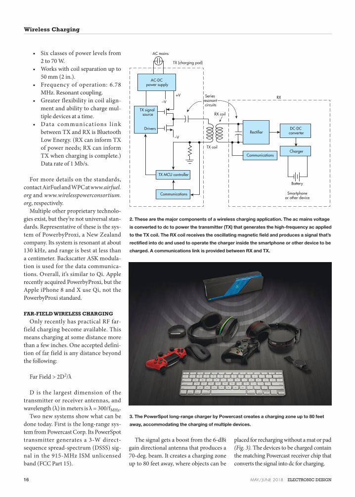
2. These are the major components of a wireless charging application. The ac mains voltage
is converted to dc to power the transmitter (TX) that generates the high-frequency ac applied
to the TX coil. The RX coil receives the oscillating magnetic field and produces a signal that’s
rectified into dc and used to operate the charger inside the smartphone or other device to be
charged. A communications link is provided between RX and TX.
3. The PowerSpot long-range charger by Powercast creates a charging zone up to 80 feet
away, accommodating the charging of multiple devices.
16 MAY/JUNE 2018 ELECTRONIC DESIGN

Tadiran Batteries
2001 Marcus Ave.
Suite 125E
Lake Success,
NY 11042
1-800-537-1368
516-621-4980
www.tadiranbat.com
PROVEN
40YEAROPERATING
LIFE*
Highly remote locations call for Tadiran batteries.
Battery replacement is costly and often dangerous work. Reduce the risk with Tadiran bobbin-type lithium thionyl chloride (LiSOCl
2)
batteries. With an annual self-discharge rate of just 0.7% per year, Tadiran LiSOCl
2 batteries
enable low power consuming wireless devices to operate for up to 40 years on a single battery, up to 4 times longer than the competition. Our batteries also feature the highest capacity, highest energy density, and widest temperature range of any lithium cell, plus a glass-to-metal hermetic seal for added ruggedness and reliability in
extreme environments.
Take no chances. Take Tadiran batteries
that last a lifetime.
* Tadiran LiSOCL2 batteries feature the lowest annual self-discharge rate of any competitive battery, less than 1% per year, enabling these batteries to operate over 40 years depending on device operating usage. However, this is not an expressed or implied warranty, as each application difers in terms of annual energy consumption and/or operating environment.
ANNUAL SELF-DISCHARGE
TADIRAN
0.7%
Up to 3%
COMPETITORS
No place to replace a battery.

Wireless Charging
JUST WHAT IS wrong with cabled chargers? Wireless char-
gers are cool technology, for sure. And they do offer some
convenience. However, they seem to be solving a problem
that doesn’t exist. How hard is it to use a wired charger?
You just plug it in. We all do it every day, mostly without
thinking.
Technology lets us do things that don’t necessarily need
doing. We do it because we can. Besides, electronic engi-
neers need continuous challenges. And as it turns out, there
are many customers for those cool new products, needed or
not. As a result, dozens of companies are now pursuing the
complex wireless-charging space.
Here’s a breakdown of the real pros and cons of wireless
charging:
PRO
• Convenience.
• No messy cables that always seem to get lost.
Ability to charge multiple devices with one charger instead
of the multiple cables usually needed.
CON
• More expensive than a plain old cable charger.
• Charging pads not as portable as a cable.
• Uses more power than a cable charger.
• Careful positioning of the devices on the charger is a
nuisance.
• Adds to the growing cloud of EMI.
Despite whatever downsides are perceived, most market
projections are rosy. Market research firm Technavio says
that the market will grow by more than 33% by 2020. And
ABI Research forecasts over 700 million wireless chargeable
devices by 2020.
CORDLESS CHARGERS: AN ALTERNATE
VIEW
This new system can handle up to about 30 products
depending on their requirements. Charge times will vary with
distance between devices and transmitter, but generally most
devices will charge fully overnight.
Another far-field charging product comes from Energous
Corp. Its WattUp system uses the unlicensed 5.85- to 5.875-
GHz band (FCC Part 18). The system’s most effective range
is from a few inches up to 3 feet, but it can cover up to 15 feet
with a weaker signal and longer charging. The 90-deg. beam-
width antenna pattern creates a charging zone into which mul-
tiple devices can be placed. Again, the devices must contain
the WattUp receivers. Bluetooth Low Energy is used as the link
Custom Optoelectronic Sensors Assemblies
Simplifed. Reliable. Customizable.
Wiring Harness & Connectorization
Board Assembly & Associated Electronic Components
Custom Plastic Housings for YourSpecifc Designs
TT Electronics
1645 Wallace Drive
Carrollton, TX 75006
(972) 323-2200
www.ttelectronics.com
Let us solve your optical sensing challenges.
MAY/JUNE 2018 ELECTRONIC DESIGN

between transmitter and receivers.
For these new far-field systems to
catch on, their receivers must be incor-
porated into the devices to be charged.
This may take some time, but the con-
venience of long-range charging makes
them an attractive alternative.
WIRELESS CHARGING OF
ELECTRIC VEHICLES
One big target for wireless charg-
ing is electric vehicles (EVs), and, in
fact, a wireless-charging grid is slowly
emerging. Today, EV charging is done
via heavy-duty cables. But new develop-
ments are gradually changing the land-
scape.
For example, BMW’s and Volkswa-
gen’s electric and hybrid models will
eventually incorporate a charging
receiver and coil that will match up
with a charging pad on the garage floor
or in the driveway. Public charging
stations would use a similar arrange-
ment. Pad alignment is critical for the
fastest and most efficient charging.
There’s even a vision of embedding
charging pads into roads and at inter-
sections or in parking lots for a quick
charge.
An alternative approach to coils is
being investigated that uses capacitive
coupling instead of magnetic induction.
One capacitor plate is located on the
bottom of the vehicle and the other plate
is on the charger. Capacitive coupling
allows higher frequencies to be used.
However, plate alignment is critical and
movement or changes produce capaci-
tance variations that require active
impedance matching to provide an effi-
cient transfer of power.
One company developing automotive
chargers is WiTricity Corp. Its patented
resonant technology, developed at MIT,
is a good fit for EV charging pads. It’s
more forgiving of coil alignment and
can transfer kilowatts of power effi-
ciently at distances of 10 to 20 cm. It can
also penetrate concrete, asphalt, and
wood.
Increased Reliability for Industrial Applications
New 1.27mm pitch Archer Kontrol connectors in horizontal
and vertical layouts with 12-80 pin combinations.
Designed with surface mount solder tabs for additional
board retention strength, it can withstand lateral and
twisting forces in high vibration environments.
Temperature range of -55°C to +125°C
Assists with blind mating
Fully shrouded connector system
Tested to perform up to 500 operations
www.harwin.com/kontrol
For these new far-field systems to catch on, their receivers must be
incorporated into the devices to be charged. This may take some
time, but the convenience of long-range charging makes them an attractive
alternative.

WILLIAM WONG | Senior Technology Editor
Machine-learning applications on the edge are becoming more common
and taking advantage of existing hardware.
Two things have moved deep-neural-network-
based (DNN) machine learning (ML) from
research to mainstream. The first is improved
computing power, especially general-purpose
GPU (GPGPU) improvements. The second is wider distribu-
tion of ML software, especially open-source software.
Quite a few applications are driving adoption of ML, includ-
ing advanced driver-assistance systems (ADAS) and self-
driving cars, big-data analysis, surveillance, and improving
processes from audio noise reduction to natural language
processing. Many of these applications utilize arrays of GPG-
PUs and special ML hardware, especially for handling training
that uses large amounts of data to create models that require
significantly less processing power to perform a range of rec-
ognition and other ML-related tasks.
For example, Au-Zone Technologies’ DeepView takes
advantage of the GPUs in NXP’s i.MX8. The i.MX8 is ideal
for many embedded applications, and its dual GPU allows it
to split video display and ML chores if necessary. The Deep-
View toolkit can be used for applications like industrial vision
processing or ADAS. It’s optimized for the i.MX8, like the one
found on Digi International’s ConnectCore i.MX53 (Fig. 1),
but also works on other platforms.
ML video processing requires hefty processing power that
ML DSPs, like Cadence’s Vision C5, and GPUs can provide
even on single-chip SoCs. Specialized hardware such as Intel’s
Movidius machine-learning vision chip delivers even more
performance using less power, suiting it for real-time video
processing in drones like DJI’s tiny SPARK (Fig. 2).
Industry Trends
1. Digi International’s ConnectCore i.MX53/Wi-i.MX53 runs NXP’s
i.MX8, which is able to handle machine-learning chores.
2. DJI’s SPARK uses Intel’s Movidius vision chip to augment every-
thing from object identification to gesture recognition.
Machine Learning Invades Embedded Applications
20 MAY/JUNE 2018 ELECTRONIC DESIGN

MORE POWER ON
YOUR PCB
PCB Terminal Blocks for Power Electronics
• Compact dimensions and high current carrying capacity – up to 72 A
• Fast, easy connection with Push-in CAGE CLAMP®
• Optimal handling for any application – with or without lever
• Comprehensive range covering 24 - 4 AWG
www.wago.us/powerelectronics

Machine-Learning Applications
Many ML applications are able to run without this heavy-
duty hardware. Of course, these applications can’t be process-
ing 4K video streams either. On the other hand, doing basic
image recognition on a low-resolution image that’s taken once
a second is something that many platforms (e.g., an ARM
Cortex-M4F) can easily handle.
OPEN SOURCE
A number of ML frameworks—Caffe and TensorFlow, to
name two—are open-source projects. However, many products
are not. Nonetheless, quite a few open-source ML models are
available for a host of applications that have already been trained.
These are often used in applications like academic robot research
programs, where cost could eliminate the use of some tools.
Still, many open-source projects build on these frame-
works, such as H2O.ai’s H2O. H2O is a tool that greatly
simplifies the creation and tuning of ML models that would
otherwise require someone with significant ML experience.
H2O’s AutoML brings the creation of ML models to a higher
level, enabling non-ML experts to more easily select and refine
models and train them.
One of the other two alternatives to H2O is to employ exist-
ing models that may be trained or have been trained and use
them on embedded platforms. The other option is to build a
new model from scratch, which can take a good bit of exper-
tise and experimentation.
ML doesn’t fit into every application, and not all embed-
ded platforms will have the memory or computing power
to incorporate ML technology where appropriate. However,
the improving hardware and availability of ML software
makes it possible to use the technology in more applications
these days.
One of the other two alternatives to H2O is to employ existing
models that may be trained or have been trained and use them
on embedded platforms. The other option is to build a new model from
scratch, which can take a good bit of expertise and experimentation.
22 MAY/JUNE 2018 ELECTRONIC DESIGN

Manufacturers focus in on durable contacts, rugged shells, watertight seals, and
different types of locking mechanisms to enable connectors to handle harsh
environments.
Connectors Toughen Up
to Battle the Elements
CABE ATWELL | Contributing Editor
Rugged and harsh environ-
ments can wreak havoc
on electrical systems and
their connectorsÑvibra-
tion, temperature extremes, chemicals,
and other fluids can (and will) render
those systems useless if their connec-
tions become compromised. Nearly
every industry has some form of envi-
ronment thatÕs detrimental to sophisti-
cated electronic systems, and because
theyÕre the entry point to those systems,
connectors are on the front lines.
Applications in mining are subjected
to dust, shock, and vibration; offshore
oil rigs and other marine services have
to deal with saltwater corrosiveness; and
aerospace applications routinely under-
go extreme temperature and pressure
fluctuations. As a result, connectors have
been designed to withstand those envi-
ronments and maintain their integrity.
To help defend connectors against
hazardous operating conditions, man-
ufacturers have added new features in
their designs, which include durable
contacts, rugged metal or thermoplas-
tic shells, watertight seals, and various
locking mechanisms.
Rugged metal casings and thermo-
plastic shells need to be manufactured
from quality materials to withstand
years of exposure to harsh environ-
ments. Metal housings must be able to
stand up against repeated shock, vibra-
tion and sudden impact, while thermo-
plastic needs to be engineered to defend
against chemicals/fluids and tempera-
ture extremes. Depending on the appli-
cation, these can come in many different
forms, including rectangular and cylin-
drical body shapes, and feature secure
locking systems to keep them mated.
Shells and casings can be manufac-
tured using a variety of materials to
meet the requirements of their oper-
ating environment. Common metals
range from aluminum and stainless steel
to brass and titanium, while thermo-
plastics and composites include nylon
and glass-filled polymers such as PEEK,
PEI, and PPS.
Fluid-resistant seals are critical for
operation in harsh environments, as
they help mitigate any intrusion from
dust, chemicals, and water. Silicone
seals and grommets need to function
flawlessly to provide a maximum seal
to outside contamination. They must
also retain their flexibility across a wide
range of temperature extremes without
degradation.
Product Trends
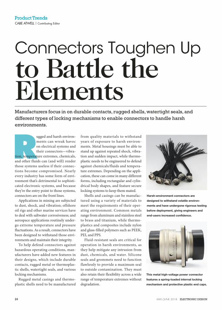
Harsh-environment connectors are
designed to withstand volatile environ-
ments and have undergone rigorous testing
before deployment, giving engineers and
end-users increased confidence.
This metal high-voltage power connector
features a spring-loaded internal locking
mechanism and protective plastic end caps.
24 MAY/JUNE 2018 ELECTRONIC DESIGN

© 2
01
8 R
och
este
r E
lectr
on
ics,
LLC
. A
ll R
igh
ts R
ese
rve
d.
02
05
20
18
THE GENUINE ARTICLE.
100% Authorized and Guaranteed.
Licensed by over 70 leading manufacturers.

Ruggedized Connectors
Contact alignment is another cru-
cial element for electrical connectors
intended for rugged environments.
Locking mechanisms that snap onto or
into the mating surface help to ensure
the internal contacts slide together per-
fectly when mated, with some produc-
ing an audible click when successfully
engaged. These include threaded cou-
pling rings, push-latches, lever locks,
and jackscrews that clamp the connec-
tor and surface together. Many connec-
tors are also outfitted with wedge locks
and TPAs (terminal position assurance)
that offer additional keying options and
further connection stability with both
the contact barrel and mating surface.
Internal contacts or pins represent
another vital aspect of harsh environ-
ment connectors. If the flow of signal
or power becomes disrupted, then the
The MIL-DTL-38999 nickel plated polymer connector is designed
for use in rugged environments. (Source: Abaillieul via Wikipedia)
Choosing the right connectors is paramount when operating in harsh envi-
ronments such as this sea-based oil rig. (Source: Jim Hatter via Wikipedia)

electrical equipment and applications will fail. Contacts
often consist of different metals that resist corrosion and
offer superior power and signal transmission, with one to
form the shape and the other for plating. They come in a
wide range of metals; however, copper forms and nickel plat-
ing are the most common.
Harsh and rugged connectors are manufactured under
strict regulations that must adhere to industry standards,
which falls under the International
Protection Marking or IP Code del-
egated by the International Electro-
technical Commision (IEC). The codes
feature a pair of digits to signify robust
particle protection and liquid ingress
protection. Therefore, an IP rating of
IP67 designates the connector is entire-
ly secure against solid debris and can
be submerged in fluid up to one meter
in depth.
The European Union has gone
beyond the IP rating system to include
the ATEX directive, which outlines
protections against explosions in the
working environments. Connectors
must be designed and tested to ensure
no electrical arcing or sparking can
happen in volatile situations where
flammable gases, vapors, and other
explosive materials are present. The
directive offers a similar number sys-
tem as IP codes, but is broken down
into six zones ranging from 0 (places
where flammable gas, vapors, and mist
are continuously present) to Zone 22
(places where explosive dust may be
present for short periods of time).
Harsh-environment connectors
are designed with engineers in mind,
meaning they’re as easy to use and ser-
vice in the field as they are on the man-
ufacturing floor. This helps reduce the
training and service time in the field.
At the same time, it aids in lowering the
costs associated with equipment ser-
vicing and training processes, thereby
improving efficiency.
When choosing the right connector,
careful consideration of the environ-
ment is mandatory. Asking the right
questions can help determine the opti-
mal connector. Some of the questions
engineers should be asking include:
What kind of terminations and types are necessary?
Are there size or space constraints?
Is sealing needed for protection against water or other fluids?
Is the connector for signal or electrical purposes?
Although the selection criteria are extensive and can quickly
become confusing, most manufacturers offer services to guide
you through the myriad options to pinpoint the most efficient
connector design.
GO TO ELECTRONICDESIGN.COM 27

Connecting Minds. Exchanging Ideas.
The 2018 IEEE MTT-SInternational Microwave Symposium
5G Summit, Tuesday, 12 June 2018; Room 103
The 5G Summit, at the Pennsylvania Convention Center in Philadelphia, is an IEEE event that is organized by two of IEEE’s largest societies – MTT-S and ComSoc. This special collaboration, for the second year running, complements MTT-S’ “hardware and systems” focus with ComSoc’s “networking and services” focus. The one-day Summit features talks from experts from government, academia, and industry experts on various aspects of 5G services and applications. It’s further complemented by the 5G Pavilion at the IMS2018 exhibition where table top demonstrations and “fi re-side” chats are presented at the 5G theater.
Other featured presentations from Huawei, GM, Keysight, NI, Global Foundries, MACOM as well as academia will include following topics:
Lunchtime Panel session: “mmWave Radios in Smartphones: What they will look like in 2, 5, and 10 years”
“Bringing the World Closer Together”
Jin BainsHead of Connectivity, SCL, Facebook
“AT&T Perspectives on 5G Services”
David LuVice President, AT&T
• The RF/Microwave Signal Chain
• Network Characteristics, Analysis and Measurement
• Fundamentals of RF Simulation
• Impedance Matching & Device Modeling Basics
• Introduction to RF and Microwave Filters
• Spectral Analysis and Receiver Technology
• Signal Generation
• Modulation and Vector Signal Analysis
• Microwave Antenna Basics
• Introduction to Radar and Radar Measurements
5G Summit Speakers:
For complete details on IMS and Microwave Week visit www.ims2018.org
• Spectrum/Regulatory• Infrastructure/Trials, Applications• Technologies, Circuits, Systems
• Design, Test & Measurement Challenges• Test-bed Services for 5G
Enhance your IMS Experience with these
Join Us in
RF Boot Camp, Monday, 11 June 2018; Room 109B
This one-day course is ideal for newcomers to the microwave world, such as technicians, new engineers, college students, engineers changing their career path, as well as marketing and sales professionals looking to become more comfortable in customer interactions involving RF & Microwave circuit, and system concepts and terminology. The format of the RF Boot Camp is like that of a workshop or short course, with multiple presenters from industry and academia presenting on a variety of topics including:

Physicians Panel Session:
Utilization of RF/Microwaves in Medicine, Thursday, 14 June 2018; Room 204B
Over the past three decades, collaboration between physicians and engineers has increased dramatically, to the benefi t of our society. Biomedical engineering departments, the majority of which found in engineering schools and some within medical schools, offer seemingly unlimited opportunities and continue to attract a large number of students. To benefi t from the merits of interdisciplinary cooperation and facilitate the transfer of technology to the market, existing large corporations, start-up medical companies, and research funding agencies now demand strong collaboration between engineers and physicians. With this in mind, IMS 2018 has made the subject of RF/microwaves in Medicine a major theme of the conference. The physicians on this panel will discuss the use ofRF/microwaves in their respective fi elds. Topics ranging from microwave hyperthermia therapy for reoccurrencesof breast cancer, advances in RF renal denervation, to back pain management using RF, will be highlighted!
Panelists:
1. Andrew Ng, Thomas Jefferson University Hospital, Philadelphia, PA 2. Daniel Frisch, Thomas Jefferson University Hospital, Philadelphia, PA 3. Donald Mitchell, Thomas Jefferson University Hospital, Philadelphia, PA 4. Ernest Rosato, Thomas Jefferson University Hospital, Philadelphia, PA 5. Eugene Viscusi, Thomas Jefferson University Hospital, Philadelphia, PA 6. Francis Kralick, Neurological Surgery, Shore Medical Center, Brigantine, NJ 7. Hamid RS Hosseinzadeh, School of Osteopathic Medicine, Stratford, NJ 8. Mark Hurwitz, Thomas Jefferson University Hospital, Philadelphia, PA 9. Nicholas Ruggiero, Thomas Jefferson University Hospital, Philadelphia, PA10. William Jow, Medifocus Inc., Columbia, MD
Exhibition Dates and Hours
Tuesday, 12 June 2018 09:30 to 17:00
Wednesday, 13 June 2018 09:30 to 17:00Exhibit-Only Time: 13:30 to 15:10Industry Hosted Reception: 17:00 to 18:00
Thursday, 14 June 09:30 to 15:00
MicroApps
The Microwave Application seminars (MicroApps) offered Tuesday, 12 June through Thursday, 14 June, 2018, provide a unique forum for the exchange of ideas and practical knowledge related to the design, development, production, and test of products and services. MicroApps seminars are presented by technical experts from IMS2018 exhibitors with a focus on providing practical information, design, and test techniques that practicing engineers and technicians can apply to solve the current issues in their projects and products.
Industry Workshops
The Industry Workshops are 2-hour industry-led presentations featuring hands-on, practical solutions often including live demonstrations and attendee participation. These Workshops are open to all registered Microwave Week attendees at a nominal charge.
PENNSYLVANIA CONVENTION CENTER • PHILADELPHIA, PENNSYLVANIA, USAExhibition Dates: 12–14 June 2018 • Symposium Dates: 10–15 June 2018
#IMS2018
Follow us on:
Philadelphia!not to miss events! Register Today!
BILL SCHWEBER | Contributing Editor
Sensing current by measuring voltage across a resistor is simple and elegant,
but issues arise with the electrical interface, sizing and selection, and thermal/
mechanical considerations.
Using Resistors for Current Sensing:
It’s More Than Just I = V/R
Measuring dynamic
current flow has
a lways been an
important param-
eter for managing system performance,
and doing so has become even more so
with the proliferation of smarter man-
agement functions for devices and sys-
tems. The most-common way to accu-
rately make this measurement is by using
a sense resistor of known value inserted
in series with the load, then measuring
the IR voltage drop across this resistor.
By applying Ohm’s law, determination
of the current flow is simple—or at least
that’s how it seems.
While using a resistor is an effective
and direct basis for such sensing, it also
has many design issues and subtleties
despite its clarity. These span the electri-
cal interface, resistor sizing and selection,
and many mechanical considerations:
THE ELECTRICAL INTERFACE
Do you go with high-side or low-side
sensing? In low-side sensing, the resistor
is placed between the load and “ground”
(or, in many cases, circuit “common”)
(Fig. 1), which enables the voltage-sens-
ing circuit to also be connected directly
to ground. While components in this
topology aren’t subject to any high-
voltage issues, it’s often undesirable and
even unacceptable, for two reasons.
First, doing so means the load itself
isn’t grounded, which is impractical for
mechanical reasons in many installa-
tions. For example, having an unground-
ed starter motor in a car and insulating it
from the chassis is a design and mount-
ing challenge. It also mandates the need
for a return wire that can carry the load
current back to the source, rather than
using the chassis. Second, even if wir-
ing and mounting aren’t considerations,
placing any resistance between the
load and ground (common) negatively
affects the control-loop dynamics and
control.
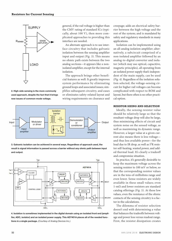
The solution is to use high-side sens-
ing, with the resistor instead placed
between the power rail and the load
(Fig. 2). This eliminates the problems
created by ungrounding the load, but
a new issue arises. The circuitry that
senses the voltage across that resistor
now can’t be grounded, which means a
differential or instrumentation ampli-
fier is used. This amplifier must have a
common-mode voltage (CMV) rating
that’s higher than the rail voltage. In
Engineering Essentials
1. Low-side sensing places the resistor
between the load and common; it simplifies
the interface to the voltage-reading analog
front end but brings problems with load
integrity and control.
30 MAY/JUNE 2018 ELECTRONIC DESIGN

!"#$ %&'()'*()+)()),-./&'()'*()+)()),0
12
.31
!(*(4 !"
!5(-(4 #$%&'(!)*"+
"(+%*(4 "
('6'6(4 , !"!%-.
"(0(4 ))
('-).(4 !
78-6
-6%9-%9!(*(4
%%1
!"#$ %&'()'*()+)()),-./&'()'*()+)()),0
12
/ !0"(0 1 * 1
%1 2!! 113!
,4'5)6) /
86%9'%9
$"(0(4
!"#$ %&'()'*()+)()),-./&'()'*()+)()),0
12
'66'666 :
!)7 !" 8 &! . 9!)1!! 4:!*-.,4'5)6) ";'/
;66%9866%9
$!(+(4
!78;
!"#$ %&'()'*()+)()),-./&'()'*()+)()),0
12
"( !1
<
%"46$!"1=
>& 1 +"+
2%"'"-")5
!"1=6
!9 $/!. $
!" !%-. "/65
!" 6 )%-. "'"-")5" !%-. "/5)" ) !%-. "%)5!" ! )%-. "%)$!" ! )%-. "?6$!" ! !%-. "4"!5!" !%-. "46$
" 3 !%-. "4)$
<'0,-
<'0,-
<'0,-
<'0,-
Resistors for Current Sensing
general, if the rail voltage is higher than
the CMV rating of standard ICs (typi-
cally, about 100 V), then more com-
plicated approaches to providing this
interface are needed.
An alternate approach is to use inter-
face circuitry that includes galvanic
isolation between the sensing amplifier
input and output (Fig. 3). This means
no ohmic path exists between the two
analog sections—it appears like a non-
isolated amplifier, except for the internal
isolation.
The approach brings other benefi-
cial features as well: It greatly improves
system performance by eliminating
ground loops and associated issues; sim-
plifies subsequent circuitry, and eases
or eliminates safety-related layout and
wiring requirements on clearance and
creepage; adds an electrical safety bar-
rier between the high voltage and the
rest of the system; and is mandated by
safety and regulatory standards in many
applications.
Isolation can be implemented using
an all-analog isolation amplifier; alter-
natively, a subcircuit comprised of a
non-isolated amplifier followed by an
analog-to-digital converter and isola-
tor (which may use optical, capacitive,
magnetic principles), all operating from
an isolated power supply that’s indepen-
dent of the main supply, can be used
(Fig. 4). Regardless of the isolation solu-
tion selected, the voltage-sensing cir-
cuit for higher rail voltages can become
complicated with respect to BOM and
layout, but there often is no other practi-
cal option.
RESISTOR SIZING AND SELECTION
Ideally, the sensing resistor value
should be relatively large so that the
resultant voltage drop will also be large,
thus minimizing effects of circuit and
system noise on the sensed voltage, as
well as maximizing its dynamic range.
However, a larger value at a given cur-
rent also means there is less voltage—
and thus less available power—for the
load due to IR drop, as well as I2R resis-
tor self-heating, wasted power, and add-
ed thermal load. It’s clearly a tradeoff
and compromise situation.
In practice, it’s generally desirable to
keep the maximum voltage across the
sensing resistor to 100 mV or below, so
that the corresponding resistor values
are in the tens-of-milliohms range and
even lower. Sense resistors are widely
available in these small values; even
1-mΩ and lower resistors are standard
catalog offerings (Fig. 5). At these low
values, even the resistance of the ohmic
contacts of the sensing circuitry is a fac-
tor in the calculations.
The dilemma of resistor selection
doesn’t end with determining a value
that balances the tradeoffs between volt-
age and power loss versus readout range.
First, the resistor dissipation creates
2. High-side sensing is the more commonly
used approach, despite the fact that it brings
new issues of common-mode voltage.
Input
Isolation barrier
Demodulator or
conditioner
Modulator or driver
Input amplifier
Output amplifier
Output
3. Galvanic isolation can be achieved in several ways. Regardless of approach used, the
result is signal information is passed across a barrier without any ohmic path between input
and output.
4. Isolation is sometimes implemented in the digital domain using an isolated front end (ampli-
fier, ADC, isolator) and an isolated power supply. This AD7401A places all of the needed func-
tions in a single package. (Courtesy of Analog Devices Inc.)
32 MAY/JUNE 2018 ELECTRONIC DESIGN
Design Note
All registered trademarks and trademarks are the property of their respective owners.
Active Rectifier Controller with Ultrafast Transient Response and Low Power Dissipation
Introduction The LT8672 is an active rectifier controller that (along with a MOSFET) provides reverse current protection and rectification for power supplies in automotive environments. This job is traditionally taken on by a Schottky diode, over which the LT8672’s active protection has a number of advantages:
• Minimal power dissipation
• Small, predictable, regulated 20mV voltage drop
The LT8672 also includes a number of features to satisfy supply rail requirements in automotive environments:
• Reverse input protection to –40V
• Wide input operation range: 3V to 42V
• Ultrafast transient response
• Rectifies 6VP-P up to 50kHz; rectifies 2VP-P up to 100kHz
• Integrated boost regulator for the FET driver performs better than charge pump devices
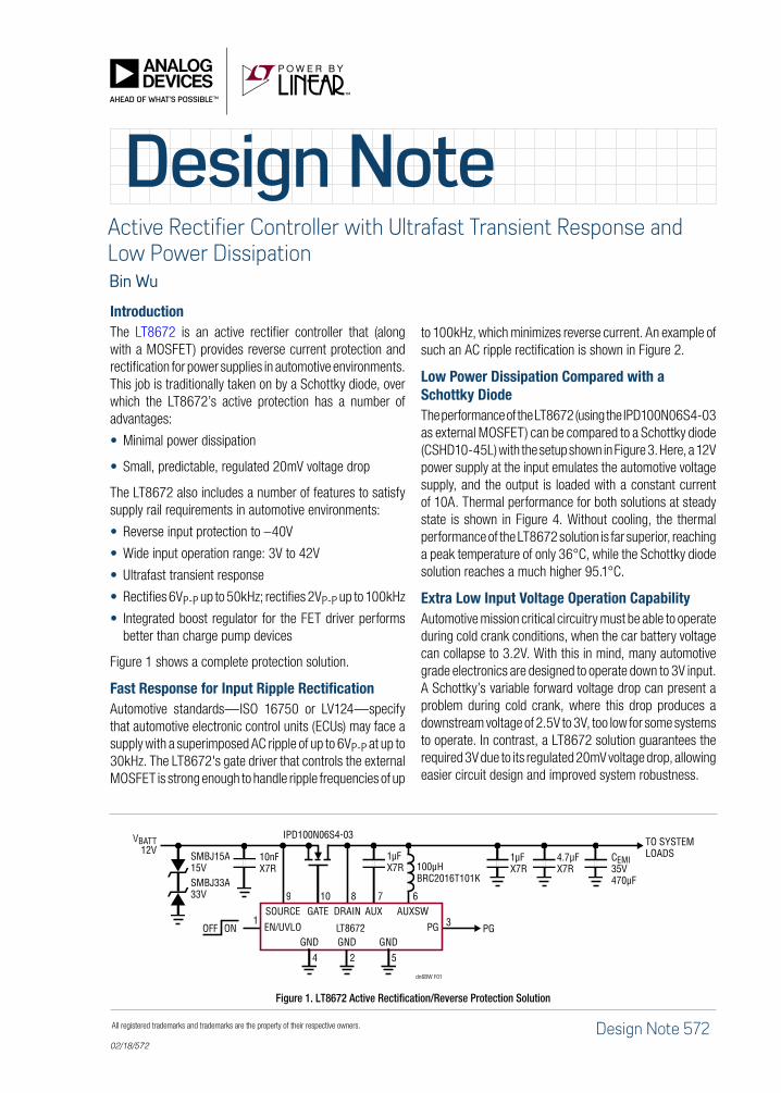
Figure 1 shows a complete protection solution.
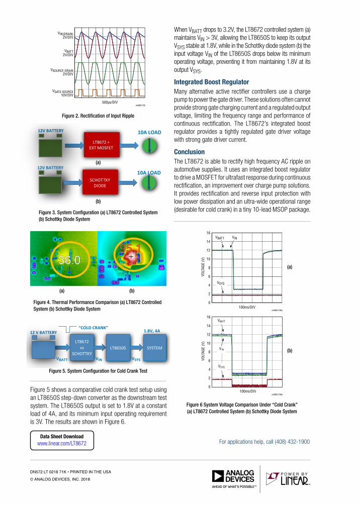
Fast Response for Input Ripple RectificationAutomotive standards—ISO 16750 or LV124—specify that automotive electronic control units (ECUs) may face a supply with a superimposed AC ripple of up to 6VP-P at up to 30kHz. The LT8672's gate driver that controls the external MOSFET is strong enough to handle ripple frequencies of up
to 100kHz, which minimizes reverse current. An example of such an AC ripple rectification is shown in Figure 2.
Low Power Dissipation Compared with a Schottky DiodeThe performance of the LT8672 (using the IPD100N06S4-03 as external MOSFET) can be compared to a Schottky diode (CSHD10-45L) with the setup shown in Figure 3. Here, a 12V power supply at the input emulates the automotive voltage supply, and the output is loaded with a constant current of 10A. Thermal performance for both solutions at steady state is shown in Figure 4. Without cooling, the thermal performance of the LT8672 solution is far superior, reaching a peak temperature of only 36°C, while the Schottky diode solution reaches a much higher 95.1°C.
Extra Low Input Voltage Operation Capability Automotive mission critical circuitry must be able to operate during cold crank conditions, when the car battery voltage can collapse to 3.2V. With this in mind, many automotive grade electronics are designed to operate down to 3V input. A Schottky’s variable forward voltage drop can present a problem during cold crank, where this drop produces a downstream voltage of 2.5V to 3V, too low for some systems to operate. In contrast, a LT8672 solution guarantees the required 3V due to its regulated 20mV voltage drop, allowing easier circuit design and improved system robustness.
02/18/572
Figure 1. LT8672 Active Rectification/Reverse Protection Solution
Design Note 572
Bin Wu
10nFX7R
IPD100N06S4-03
9
1
10 8 7 6
3
1µFX7R 100μH
BRC2016T101K
VBATT12V
1µFX7R
4.7µFX7R
CEMI35V470µF
dn6BW F01
ONOFF
SOURCE GATE DRAIN AUXSWAUX
PGEN/UVLO
2
GND
4
GND
5
GND
SMBJ15A15VSMBJ33A33V
LT8672
TO SYSTEM LOADS
PG
For applications help, call (408) 432-1900
© ANALOG DEVICES, INC. 2018
DN572 LT 0218 71K • PRINTED IN THE USA
Data Sheet Downloadwww.linear.com/LT8672
LT8672 +EXT MOSFET
10A LOAD12V BATTERY
SCHOTTKYDIODE
12V BATTERY10A LOAD
(a)
(b)
(a) (b)
Figure 3. System Configuration (a) LT8672 Controlled System (b) Schottky Diode System
Figure 4. Thermal Performance Comparison (a) LT8672 Controlled System (b) Schottky Diode System
Figure 5. System Configuration for Cold Crank Test
Figure 5 shows a comparative cold crank test setup using an LT8650S step-down converter as the downstream test system. The LT8650S output is set to 1.8V at a constant load of 4A, and its minimum input operating requirement is 3V. The results are shown in Figure 6.
LT8672vs
SCHOTTKY
12 V BATTERY
LT8650S SYSTEM
VBATT
“COLD CRANK”
VIN VSYS
1.8V, 4A
Figure 2. Rectification of Input Ripple
500µs/DIV
VIN(DRAIN)2V/DIV
VBATT2V/DIV
VSOURCE-DRAIN2V/DIV
VGATE-SOURCE10V/DIV
dn6BW F02
When VBATT drops to 3.2V, the LT8672 controlled system (a) maintains VIN > 3V, allowing the LT8650S to keep its output VSYS stable at 1.8V, while in the Schottky diode system (b) the input voltage VIN of the LT8650S drops below its minimum operating voltage, preventing it from maintaining 1.8V at its output VSYS.
Integrated Boost Regulator Many alternative active rectifier controllers use a charge pump to power the gate driver. These solutions often cannot provide strong gate charging current and a regulated output voltage, limiting the frequency range and performance of continuous rectification. The LT8672’s integrated boost regulator provides a tightly regulated gate driver voltage with strong gate driver current.
Conclusion The LT8672 is able to rectify high frequency AC ripple on automotive supplies. It uses an integrated boost regulator to drive a MOSFET for ultrafast response during continuous rectification, an improvement over charge pump solutions. It provides rectification and reverse input protection with low power dissipation and an ultra-wide operational range (desirable for cold crank) in a tiny 10-lead MSOP package.
Figure 6 System Voltage Comparison Under “Cold Crank” (a) LT8672 Controlled System (b) Schottky Diode System
100ms/DIV
VOLT
AGE
(V)
16
14
12
10
8
6
4
2
0
dn6BW F06a
VBATT
VSYS
VIN
100ms/DIV
VOLT
AGE
(V)
16
14
12
10
8
6
4
2
0
dn6BW F06b
V BATT
V IN
V SYS
100ms/DIV
(a)
(b)

2018 Platinum Sponsor
Resistors for Current Sensing
self-heating, which means the selected
resistor type must have a suitable power
rating, and it must be derated at higher
temperatures.
Also, any self-heating will cause the
resistor to drift from its nominal val-
ue. How much it drifts depends on the
material and construction of the sense
resistor. A standard chip resistor has a
temperature coefficient of resistance
(TCR) of about ±500 ppm/°C (equal to
0.05%/°C), while standard sense resis-
tors fabricated with special material
and construction techniques are avail-
able with TCRs of ±100 ppm/°C, down
to about ±20 ppm/°C. There are even
precision-performance units offered
(at a much-higher cost) down to ±1
ppm/°C.
Note that using a snip of copper wire
or PC-board track might seem like a
good way to get a milliohm-valued sense
resistor at nearly zero cost. However, the
TCR of copper is around 4000 ppm/°C
(0.4%/°C), which is orders of magnitude
inferior to a low-TCR sense resistor.
In some cases, a viable tactic for
reducing the temperature rise due to
self-heating is to use a larger-wattage,
which will be less affected by self-heat-
ing. But these, too, have a somewhat
higher component cost and larger foot-
print. The designer must do a careful
analysis of the current, the dissipation,
the effects of TCR, and any derating
needed for long-term reliability and per-
formance.
MECHANICAL CONSIDERATIONS
At very low current levels, the phys-
ical size of the current-sense resistor is
about the same as other resistors. But
physically larger resistors are needed
as wattage rating increases, and this
wil l have an impact on both PC-
board layout—assuming the resistor
is board-mounted—and the thermal
situation of the both the resistor and
its surroundings.
For the higher-rated resistors, place-
ment and mounting becomes a serious
issue; PC-board surface mounting may
not be an option; and real estate and
thermal issues increase significantly.
Larger units may even need mounting
brackets or hold-downs to keep motion
and vibration effects down to an accept-
able minimum.
The difficulty of making the “simple”
electrical connections shouldn’t be
overlooked either. When wires are car-
rying tens or even hundreds of amps,
the connections between those wires
and the resistor’s terminations need
careful planning and larger, more rug-
ged surfaces, which, of course, may
include screws and clamps. Just think
of the typical internal-combustion car
battery that must deliver over 100 A to
start the car, from a modest 12-V bat-
tery. Even 100-mΩ contact resistance at
the battery plus terminal translates to a
supply loss of 1.2 V, in a scenario where
there isn’t much voltage headroom.
In addition, even though the sensed
voltage is low, the common-mode volt-
age may not be low, and the connec-
tions may be carrying high currents.
As a result, there are safety and access
issues that will affect cabling, routing,
possible short circuits, and accessibil-
ity. Further, the designer must plan
where and how to connect the relatively
thin-gauge voltage-sensing wires to the
contacts that also carry the higher load
current. Resistance of the sensing-wire
contacts may look like resistance that’s
part of the sense resistor itself, and so
the I = V/R calculations need to factor
in this additional resistance. Even the
TCR of any contacts can also be an issue
in higher-accuracy situations.
Using a resistor for current sensing is
a very educational example of the chal-
lenges of going from a solution that’s
very simple in principle, to one which
works, works well, and works over the
range of expected operating conditions
of the application. Fortunately, it’s also a
solution that’s used extensively, so many
of the issues can be resolved by leverag-
ing the experience of application engi-
neers from resistor vendors or experts
in high-current sensing.
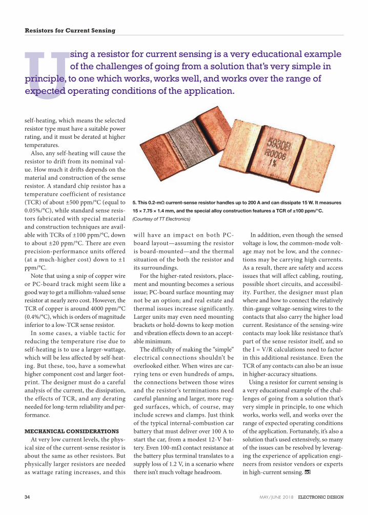
5. This 0.2-mΩ current-sense resistor handles up to 200 A and can dissipate 15 W. It measures
15 × 7.75 × 1.4 mm, and the special alloy construction features a TCR of ±100 ppm/°C.
(Courtesy of TT Electronics)
Using a resistor for current sensing is a very educational example
of the challenges of going from a solution that’s very simple in
principle, to one which works, works well, and works over the range of
expected operating conditions of the application.
34 MAY/JUNE 2018 ELECTRONIC DESIGN
MULTIPHYSICS MODELING OF A WELDING PROCESSIf you want to learn about the multiphysics modeling of
a welding process, then tune into this webinar featuring
guest speaker Stuart Brown of Veryst Engineering.
Modeling a complex thermomechanical process, such
as welding, requires the inclusion of several coupled
physics phenomena.
This webinar describes how multiphysics modeling en-
abled a simulation of a valve welding process, which was
needed to determine how a toxic leak developed. The
numerical simulation allowed a rapid bounding analysis
of the welding process and generated heat that aff ected
the polymeric seals. The simulation included the physical
processes of the deposition of weld metal, melting of the
base metal, radiative heating due to the high-tempera-
ture plasma arc, and heat of fusion of the solidifying weld
as well as tracing the weld path at diff erent amounts of
material deposition and sizes of fusion zone.
During the webinar, we will show how to create the
model in the COMSOL Multiphysics® soft ware, describe
the actual toxic release event, and discuss the testing
that was done to correlate with the numerical simulation
results. The webinar will conclude with a Q&A session.
SPEAKERS:Stuart Brown, Veryst Engineering
Dr. Stuart Brown is the managing
partner of Veryst Engineering®,
LLC, an engineering consult-
ing firm located in the Boston
area. Veryst provides services in
product design, manufacturing
processes, and failure analysis.
Dr. Brown’s technical background
includes mechanical engineering
and materials science. He has consulted in manufacturing
processes including metal and polymer manufacturing pro-
cesses, semisolid materials, extrusion, powder metallurgy,
drawing, forging, welding, and cold and hot rolling; using
engineering analysis; computational modeling; experimen-
tation; and materials characterization. He also has extensive
research and development experience in thin films and
microelectromechanical systems (MEMS). Prior to founding
Veryst Engineering, Dr. Brown was the director of the Boston
off ice of Exponent, Inc. Before Exponent, Dr. Brown was
on the faculty of the Department of Materials Science and
Engineering at MIT.
Veryst Engineering is a registered trademark of Veryst Engineering, LLC
Nicolas Huc, COMSOLNicolas Huc joined COMSOLcFrance in 2004 and is currently
the head of their development
team. He is also the manager of
the Heat Transfer Module. Nicolas
studied engineering at ENSIMAG
before receiving his PhD in living
system modeling from Joseph
Fourier University.
FREE WEBINAR | June 21, 2018 | 2:00pm ET
Registration URL:
https://event.on24.com/wcc/r/1669591/0CD81A732F26
8B5540F16F23D836ED61
Visualization of temperature and temperature gradient fields in a welding process in which the arc moves along the weld joint.

Though its exact format for widespread use needs to be ironed out, TSN is primed to
take over for standard Ethernet in industrial settings due to its superiority in terms of
latency.
What’s the Difference Between
Ethernet and Time-Sensitive Networking?
VOLKER E. GOLLER | Systems Applications Engineer, Analog Devices Inc.
www.analog.com/en/index.html
These days, anyone working
in industrial communica-
tions is bound to come up
against the topic of time-
sensitive networking (TSN). TSN will
definitely get here. The only thing that
still must be clarified is when and in
what form. However, even today, the its
advantages for industrial communica-
tions aren’t always clear.
HISTORY
Ethernet was introduced to offices in
the early 1980s and quickly became very
popular due to its high throughput of (at
that time) a sensational 10 Mb/s. How-
ever, this Ethernet wasn’t practical for
real-time applications because it used a
common medium known as a party line.
Collisions occurring at high utilization
rates caused problems in office settings.
In the next step of its development,
collisions were eliminated through the
introduction of switched networks. In
addition, with quality of service (QoS),
Ethernet datagram prioritization was
introduced (Fig. 1).
For industrial applications, guaran-
teed latency is particularly important.
Despite QoS, standard Ethernet as used
in offices can only guarantee latencies
up to a certain point, especially with
high network utilization.
There are several reasons for this,
with the main issues being the store-
and-forward strategy commonly used
in commercial multiport switches and
the fact that it’s impossible to reserve
bandwidth.
Store and forward means that a
switch receives a complete datagram
before forwarding it. This has advan-
tages in terms of processing in the
switch, but it also brings potential
problems that can negatively impact
latency and reliability:
What’s the Difference?
1. In this Ethernet frame, data fields relevant
to TSN data-flow identification are shown in
green.
36 MAY/JUNE 2018 ELECTRONIC DESIGN

• When going through a switch, a
datagram is delayed by an amount
depending on its length. If switch-
es are cascaded, the effect is mag-
nified.
• Because a switch doesn’t have an
infinite storage capacity, it can
reject datagrams if the network is
experiencing overutilization (too
much traffic); this means that data-
grams—even those given higher
priority—can simply be lost.
• Long datagrams can block a port
for relatively long times.
Switch cascading posed a challenge in
industrial environments right from the
start. Apart from the star topology used
in the IT field, line, ring, and tree topol-
ogies are frequently used in automation
(Fig. 2). These adapted topologies signif-
icantly reduce Ethernet installation wir-
ing requirements and costs. Hence, in
industry, two-port switches employing a
cut-through strategy are integrated into
field devices. Cut-through means that
datagrams are forwarded before being
completely received.
ONE SIZE FITS IT ALL: INDUSTRIAL
ETHERNET UP TO NOW
Because classic Ethernet did not have
sufficient capabilities for bandwidth
reservation, automation experts began
developing their own Ethernet exten-
sions in 2000. However, the paths they
took differed greatly. Differentiation is
made between the following approaches:
• Protocols using Ethernet as a
transport medium for a fieldbus.
These protocols claim complete
control over the Ethernet medium
for themselves. Classic TCP/IP
communications are only possible
in piggyback style via the fieldbus
(EtherCAT and POWERLINK)
or through a channel assigned by
the fieldbus (Sercos). Bandwidth
control is firmly in the hands of
the fieldbus.
2. Among the frequently used topologies in
automation are line and ring.
GO TO ELECTRONICDESIGN.COM 37
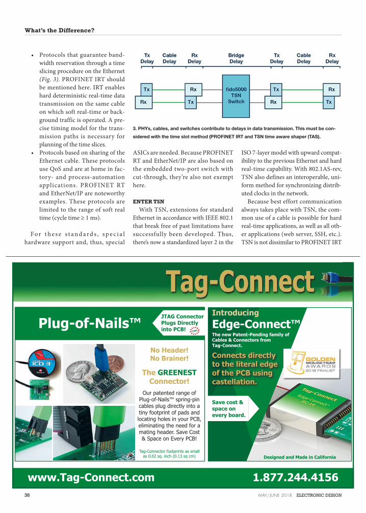
What’s the Difference?
• Protocols that guarantee band-
width reservation through a time
slicing procedure on the Ethernet
(Fig. 3). PROFINET IRT should
be mentioned here. IRT enables
hard deterministic real-time data
transmission on the same cable
on which soft real-time or back-
ground traffic is operated. A pre-
cise timing model for the trans-
mission paths is necessary for
planning of the time slices.
• Protocols based on sharing of the
Ethernet cable. These protocols
use QoS and are at home in fac-
tory- and process-automation
applications. PROFINET RT
and EtherNet/IP are noteworthy
examples. These protocols are
limited to the range of soft real
time (cycle time ≥ 1 ms).
F o r t h e s e s t a n d a r d s , s p e c i a l
hardware support and, thus, special
ASICs are needed. Because PROFINET
RT and EtherNet/IP are also based on
the embedded two-port switch with
cut-through, they’re also not exempt
here.
ENTER TSN
With TSN, extensions for standard
Ethernet in accordance with IEEE 802.1
that break free of past limitations have
successfully been developed. Thus,
there’s now a standardized layer 2 in the
ISO 7-layer model with upward compat-
ibility to the previous Ethernet and hard
real-time capability. With 802.1AS-rev,
TSN also defines an interoperable, uni-
form method for synchronizing distrib-
uted clocks in the network.
Because best effort communication
always takes place with TSN, the com-
mon use of a cable is possible for hard
real-time applications, as well as all oth-
er applications (web server, SSH, etc.).
TSN is not dissimilar to PROFINET IRT
3. PHYs, cables, and switches contribute to delays in data transmission. This must be con-
sidered with the time slot method (PROFINET IRT and TSN time aware shaper (TAS).
38
No Header!No Brainer!
The GREENESTConnector!
www.Tag-Connect.com 1.877.244.4156
Tag-Connector footprints as smallas 0.02 sq. inch (0.13 sq cm)
Our patented range ofPlug-of-Nails™ spring-pincables plug directly into atiny footprint of pads andlocating holes in your PCB,eliminating the need for amating header. Save Cost& Space on Every PCB!
Designed and Made in California
Edge-Connect™Introducing
Connects directlyto the literal edgeof the PCB usingcastellation.
The new Patent-Pending family ofCables & Connectors fromTag-Connect.
Save cost &space onevery board.
Plug-of-Nails™TINY
JTAG ConnectorPlugs Directlyinto PCB!
MAY/JUNE 2018 ELECTRONIC DESIGN

Whether you’re designing the communications system of tomorrow or connecting
the Internet of Things, you need cutting-edge product solutions to bring your
design to fruition. At KOA Speer, we’re the ideal partner to help you do just that.
Our constantly expanding line of passive components will give you the solution to
make your concept a reality!
More than just Resistors - yes we're the world leader in thick film resistors,
but our product line is broad and growing every day, including:
• Shunt/Current Sense Resistors
• Wide Terminal Resistors
• High Voltage Resistors
• Thin Film Chip Resistors
• Surge Resistors
Passive Component Solutions - our engineering group will work with your
design team to develop the passive component solution you need. Many of
the hundreds of new products we’ve introduced in recent years are the result of
such collaboration.
Award Winning Passive Supplier - we’re the industry’s most recognized and
awarded supplier for achieving the highest product quality, on-time delivery
and responsive customer service.
Make the Leap from Concept to Reality,
visit KOASpeer.com
Higher Power SurgeCurrent Resistors (SR73)
Metal Plate Current Sense Resistors (TLR)
Wide Terminal Current
Sense Resistors (WK73R1J)
From
Concept to Reality
Our new passive component solutionswill help you make the leap!
NEW! From KOA Speer

What’s the Difference?
in that regard, and it offers comparable
performance.
What’s new with TSN is the need for
more extensive network configuration.
Centralized or decentralized configura-
tion is possible. Both types of configura-
tion are currently being discussed and
implemented. Interoperability between
the two configuration mechanisms is a
future development goal.
PRACTICAL ADVANTAGES
The most common answer is that
with a larger market, less expensive
network interfaces also appear on the
market. After all, TSN will also be
found in building automation and the
automotive industry in the future. As
a matter of fact, the market for embed-
ded TSN solutions is expected to be
significantly bigger than the current
market for all industrial Ethernet solu-
tions put together.
The greatest technical advantage of
TSN over previous industrial Ethernet
methods is its scalability. Unlike cur-
rent industrial networks, TSN was not
defined for a specific transmission rate.
TSN can be used for 100 Mb/s just as for
1 Gb/s, 10 Mb/s, or 5 Gb/s.
It also enables topologies to be better
optimized because now adapted data
rates can be selected for various seg-
ments. Whether it’s Gb/s, 100 Mb/s, or
10 Mb/s, a unified layer 2—IEEE802.1/
TSN—is used.
A uniform network infrastructure
also helps personnel tasked with setting
up and maintaining the network. That’s
because, thanks to TSN, solutions
can now be used in sectors other than
automation: building, process, and
factory automation, as well as energy
distribution.
This prompts the next advantage—
the training factor. TSN is already a
topic at many universities, mostly in
the research stage. However, techni-
cal and vocational colleges are already
showing interest in this topic. It can
4. The TSN segment is combined with PROFINET and EtherCAT.
40
.18"
think...low profilefrom
ht.Over 5000 Std.
Ultra Miniature
Surface Mount(and Plug-In) Models
Audio / 400Hz / Pulse
Multiplex Data Bus /
DC-DC Converter
Transformers / Power
& EMI Inductors
PICO units manufacturedand tested to MIL-PRF-27
requirements. QPL units areavailable. Delivery stock to one
week for sample quantities.
143 Sparks Ave, Pelham, NY 10 03
Call Toll Free: 800-431-1064E Mail: [email protected]
FAX: 914-73 - 225
MILITARY•COTS•INDUSTRIAL
TRANSFORMERS & INDUCTORS
PICO Electronics Inc.
...thinksmall!
PICO
Transformersand Inductors
VISIT OUR EXCITING NEW WEBSITE
www.picoelectronics.com
Featuring our easy-to-use product Search Wizard!
See Pico’s full Catalog immediately
www.picoelectronics.com
MAY/JUNE 2018 ELECTRONIC DESIGN

be safely said that TSN will become
basic knowledge for engineers, techni-
cians, and skilled workers. Retraining
for different fieldbuses will no longer
be necessary.
BROWNFIELD, OR WHAT WILL
HAPPEN TO TODAY’S PROTOCOLS?
In nearly all TSN-related working
groups, there’s recurring theme: How to
safeguard the transition to TSN and the
supply to existing installations, such as
Brownfield applications?
On all sides, emphasis is being placed
on making it possible for customers to
easily and smoothly transition to TSN. It
can already be said today that the exist-
ing industrial Ethernet protocols aren’t
just going to vanish overnight. On the
contrary, anyone using PROFINET,
EtherNet/IP, EtherCAT, or a similarly
widespread industrial Ethernet proto-
col today can safely assume that he or
she will also be able to operate networks
with these protocols— and receive
support and replacement parts—in 10
years’ time.
All industrial Ethernet organiza-
tions provide models that describe how
existing plants can cooperate with new
TSN-based devices. The interface to
the existing industrial network is made
by a gateway (Sercos), with a coupler
(EtherCAT), or without any special
hardware (PROFINET RT) (Fig. 4). In
particular, PROFINET and EtherNet/
IP plan to make their complete proto-
cols available right on TSN as layer 2.
This makes stepwise transition to TSN
possible.
CONCLUSION
TSN will be found everywhere in new
installations, as well as in the form of
islands or segments introduced incre-
mentally into existing installations.
However, with TSN, there will be
new players in the industrial Ethernet
field. OPC UA with new transport pro-
tocol PUB/SUB, in conjunction with
TSN, is already a competitor to classic
protocols. For the manufacturers of
field devices, this means that the clas-
sic industrial Ethernet solutions, as
well as TSN and the new players, must
be supported.
VOLKER E. Goller, a systems applications
engineer with Analog Devices, has over 30
years of experience with a diverse set of in-
dustrial applications ranging from complex
motion control and embedded sensors to
time-sensitive-networking technology. A
software developer by trade, Volker has
developed a wide variety of communica-
tion protocols and stacks for wireless and
wired applications while actively engaging
in fielding new communication standards
through his involvement with leading in-
dustry organizations. He can be reached at
3D PRINTin 4 WD*
RFID
NEW
STENCIL
3D-MID
FRONT PANELin 1 WD*
PCB8 hour service
NEW
NEW
create:electronics
* W
D =
Le
ad
tim
e in
wo
rkin
g d
ays
beta-layout.com
+1 916 241 9062

Design FeaturePAUL RAKO | Contributing Editor
Bob Pease had a special love for voltage-to-fre-
quency converter circuitry. I did a vamp on his
writing in an article of my own. If you want to
measure a voltage in a remote location, it might
be easier to send a series of pulses over a long wire, rather than
send the voltage itself. The pulses are more resistant to noise,
and you can clean the noise out of the pulse signal easier than
try to reject noise out of a pure analog voltage. V-to-F circuits
also have great dynamic range and will work over several
decades of frequency.
Measuring a pulse-train frequency just requires a micro-
controller or logic circuit using a cheap accurate crystal. That
can be more cost-effective than measuring a voltage, where
you need an accurate reference chip.
Still, your system might have an accurate reference anyway.
When I designed automotive diagnostic equipment at HP,
I noted that, “You need a rock and a ref.” This was a jaunty
shorthand to say you needed a quartz crystal oscillator for
accurate time, and a good reference to measure voltage. With
those two, you can derive current, and power, and most of
whatever else you want to measure. In a way, using a V-to-F
converter means you’re pushing the reference requirement to
the sensing chip. If you can develop an accurate V-to-F circuit,
then you don’t need a separate reference chip.
Saying the V-to-F has great dynamic range is a way of saying
the output is very linear. It’s accurate over a wide range of input
voltages and output frequencies. That’s a great deal, compared
to the headaches of ensuring a sampled data system remains
accurate no matter the range of the input voltage. Once you
add attenuation and range amplifiers to a system, things get
pretty difficult and complicated.
I tried to use analog switches to make an attenuator in that
HP diagnostic equipment I worked on. I had all kinds of prob-
lems with stray capacitance and accuracy issues, so I called Jim
What’s All This LM331 Stuff, Anyhow?
1. The block diagram of the LM331 represents a relaxation oscil-
lator that will change frequency with input voltage. The output is a
pulse train, not a square wave; hence the one-shot. (Courtesy of Texas
Instruments)
2. A more detailed block diagram of the LM331 reveals the R-S flip-flop,
the internal bandgap voltage reference, and a current mirror. The band-
gap output voltage is available on pin 2, which you also use to set the
internal current mirror with a load resistor. (Courtesy of Texas Instruments)
The classic LM331 can be a great learning tool when it comes to voltage-to-frequency
conversion—one of main pillars of analog design.
42 MAY/JUNE 2018 ELECTRONIC DESIGN

±2000 V High Speed Pulse GeneratorPVX-4000 Series All-in-One High Voltage Pulse Generators
Simply set pulse width, frequency and voltage with the intuitive front panel interface, or
with your computer… It’s that easy!
With thirty years experience making high voltage pulse generators, Directed Energy is
your source for benchtop, module and custom/OEM pulsed solutions.
• 0 to ±2000 V• Pulse widths from 500 ns to DC• USB and RS-232
• Pulse rise and fall times ≤50 ns
• Repetition frequencies to 30 KHz
Directed Energy, Inc. an IXYS Companywww.directedenergy.com | +1-970-493-1901
Williams at Linear Technology, now part of Analog Devices.
He asked what I heard when I changed the vertical range on
my Tektronix scope. I said that I heard relays clicking. Wil-
liams said they used relays since doing a solid-state attenuator
is nearly impossible for high frequencies and voltages. Using a
V-to-F converter might save you all of these headaches.
THE LM331 AND V-TO-F
To understand V-to-F conversion, the LM331 datasheet is
a great place to start. The applications section was written by
Pease. Several application notes published by Texas Instru-
ments were most likely also written by Pease. These notes are
all linked to on the LM331 product page. The fundamental
app note, “Versatile Monolithic V/Fs can Compute as Well
as Convert With High Accuracy,” was released in 1980, at the
same time as the part. The app note shows both a simple and
detailed block diagram of the part (Figs. 1 and 2).
You can also use the LM331 to make a frequency-to-voltage
converter. The app note “Frequency-to-Voltage Converter
Uses Sample-and-Hold to Improve Response and Ripple”
shows how to remove the output ripple from the circuit while
still keeping a speedy response time. You can think of it as a
form of synchronous demodulation. It samples the output
voltage at the same point in the ripple waveform. This note
builds on the basic F-to-V app note, “V/F Converter ICs
Handle Frequency-to-Voltage Needs.”
Another vamp on the basic V-to-F converter is the current-
to-frequency converter. There’s another nice app note for that,
“Wide-Range Current-to-Frequency Converters.” The app
note describes ways to build on the inherent wide dynamic
range of the LM331 to make circuits that can work down to
picoamperes of input current. While you have to add a lot of
circuity to get that performance, it’s a testament to the versatil-
ity of the LM331.
Going through the drawers of my home lab bench, I uncov-
ered an LM331 voltage-to-frequency IC demo board given to
me by the folks at Boldport (Fig. 3). Dr. Saar Drimer, the elec-
tronic artist behind Boldport, packages the board in a handy
kit that you can order from his website. The kit has a Bob Pease
quote “My favorite programming language is solder.” The kit is
based on Figure 20 from the LM331 datasheet (Fig. 4).
3. The folks at Boldport make a nifty kit based on a Pease application
circuit in the LM331 datasheet.
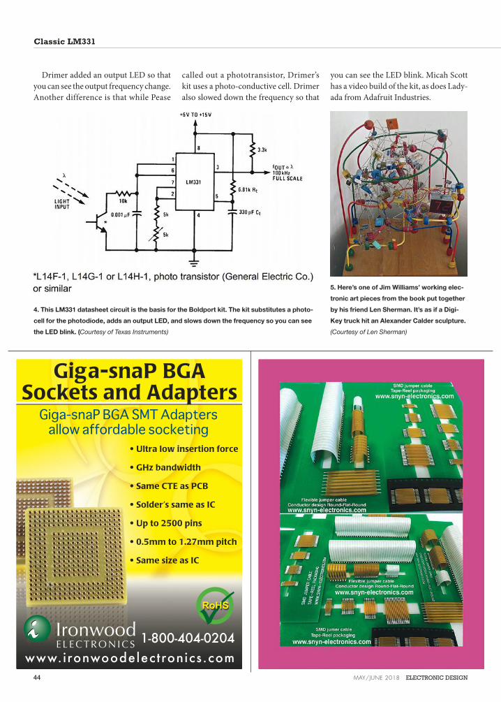
Classic LM331
Drimer added an output LED so that
you can see the output frequency change.
Another difference is that while Pease
called out a phototransistor, Drimer’s
kit uses a photo-conductive cell. Drimer
also slowed down the frequency so that
you can see the LED blink. Micah Scott
has a video build of the kit, as does Lady-
ada from Adafruit Industries.
4. This LM331 datasheet circuit is the basis for the Boldport kit. The kit substitutes a photo-
cell for the photodiode, adds an output LED, and slows down the frequency so you can see
the LED blink. (Courtesy of Texas Instruments)
5. Here’s one of Jim Williams’ working elec-
tronic art pieces from the book put together
by his friend Len Sherman. It’s as if a Digi-
Key truck hit an Alexander Calder sculpture.
(Courtesy of Len Sherman)
44
PPRoHS
MAY/JUNE 2018 ELECTRONIC DESIGN
AD INDEX
ADVERTISER NAME PAGE
Acces I/O Products ...........................45
Altech Corp. ......................................8-9
Avtech Electrosystems, LTD ...........31
Beta-Layout ......................................41
Coilcraft .............................................1
Comsol Inc. .......................................35
Dean Technology ..............................IBC
Digi-Key.......................................FC, IFC
Electronic Design Connect .............47
Hammond Mfg. Co. Inc. ..................22
Harwin ...............................................19
IMS................................................28-29
Ironwood Electronics Inc. ...............44
IXYS Colorado.............................26, 43
Keystone Electronics ........................23
Koa Speer Electronics ......................7, 39
Linear Technology...................32a/b, BC
Memory Protective Devices ............5
PCBCart (General Circuits, LTD.) ...27
Pico Electronics Inc. .........................40
Radicom Research ............................6
Rochester Electronics .......................25
Rohde & Schwarz ..............................13
Snyn Electronics Co. ........................44
Stanford Research Systems .............10
Tadiran ...............................................17
Tag Connect ......................................38
TDK-Lambda Americas, Inc. ..........37
Top 50 Electronic Distributors .......33
TT Electronics ...................................18
Vicor Corp. ........................................2
Wago Corp. ........................................21
For more information on products or services,
visit our website, www.electronicdesign.com. The
advertisers index is prepared as an extra service.
Electronic Design does not assume any liability for
omissions or errors.
THE ART OF THE SCIENCE
Most of us have heard about STEM
(science, technology, engineering, and
math). I first heard the term “STEAM”
from my pals at Evil Mad Scientist. The
added “A” stands for “art.” Boldport is an
advocate of the artistic side of engineer-
ing, as evidenced by the whimsical traces
on the LM331 Pease PCB (printed circuit
board). While the artistic aspect of cir-
cuits seems to be blooming, it’s nice to
know that analog geniuses like Jim Wil-
liams used to make working sculptures
out of electronic circuits decades ago.
Williams’ best friend, Len Sherman of
Maxim Integrated, even made up a book
of various Williams creations (Fig. 5).
We analog folks also know there’s art
in the circuit theory and the mathemat-
ics that underlay the theory. It might be
easier to buy a cheap microcontroller
from Microchip, TI, or NXP than use
an LM331. The thing is, the design and
implementation of the LM331 is worth
understanding just so you know the
principles of analog design. While chips
come and go, the principles of analog are
timeless.
45
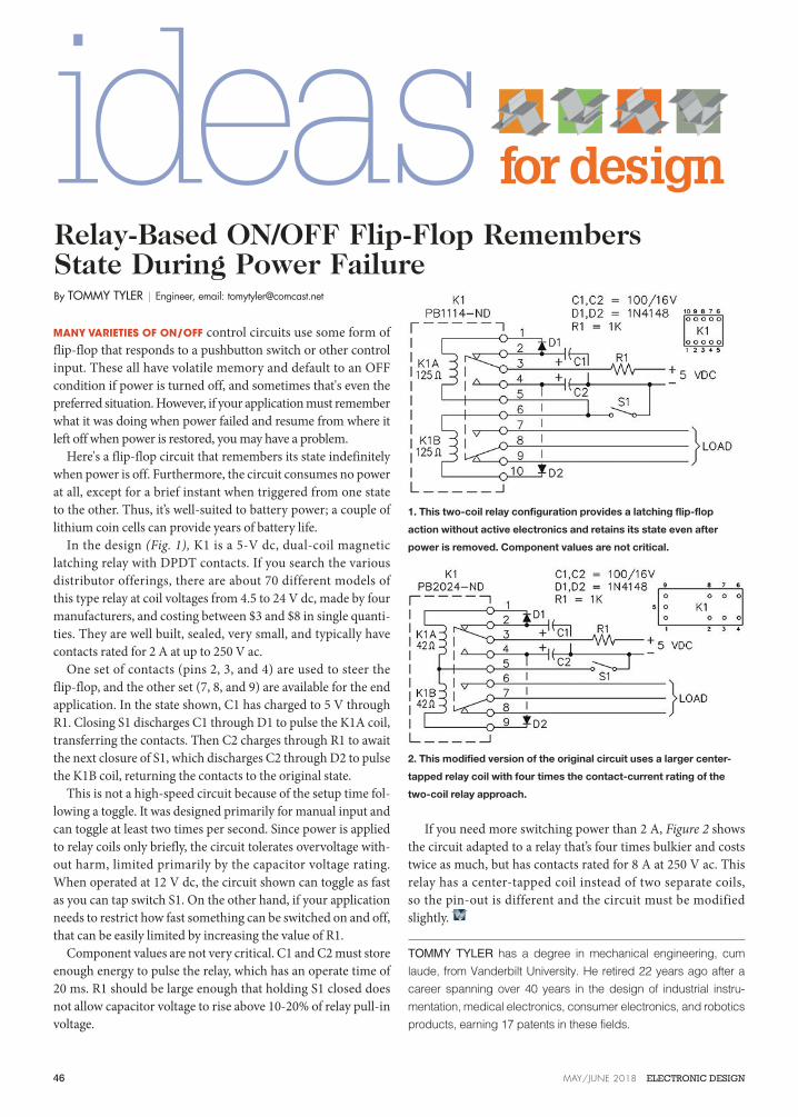
ideas for design
Relay-Based ON/OFF Flip-Flop Remembers State During Power Failure
MANY VARIETIES OF ON/OFF control circuits use some form of
flip-flop that responds to a pushbutton switch or other control
input. These all have volatile memory and default to an OFF
condition if power is turned off, and sometimes that's even the
preferred situation. However, if your application must remember
what it was doing when power failed and resume from where it
left off when power is restored, you may have a problem.
Here's a flip-flop circuit that remembers its state indefinitely
when power is off. Furthermore, the circuit consumes no power
at all, except for a brief instant when triggered from one state
to the other. Thus, it’s well-suited to battery power; a couple of
lithium coin cells can provide years of battery life.
In the design (Fig. 1), K1 is a 5-V dc, dual-coil magnetic
latching relay with DPDT contacts. If you search the various
distributor offerings, there are about 70 different models of
this type relay at coil voltages from 4.5 to 24 V dc, made by four
manufacturers, and costing between $3 and $8 in single quanti-
ties. They are well built, sealed, very small, and typically have
contacts rated for 2 A at up to 250 V ac.
One set of contacts (pins 2, 3, and 4) are used to steer the
flip-flop, and the other set (7, 8, and 9) are available for the end
application. In the state shown, C1 has charged to 5 V through
R1. Closing S1 discharges C1 through D1 to pulse the K1A coil,
transferring the contacts. Then C2 charges through R1 to await
the next closure of S1, which discharges C2 through D2 to pulse
the K1B coil, returning the contacts to the original state.
This is not a high-speed circuit because of the setup time fol-
lowing a toggle. It was designed primarily for manual input and
can toggle at least two times per second. Since power is applied
to relay coils only briefly, the circuit tolerates overvoltage with-
out harm, limited primarily by the capacitor voltage rating.
When operated at 12 V dc, the circuit shown can toggle as fast
as you can tap switch S1. On the other hand, if your application
needs to restrict how fast something can be switched on and off,
that can be easily limited by increasing the value of R1.
Component values are not very critical. C1 and C2 must store
enough energy to pulse the relay, which has an operate time of
20 ms. R1 should be large enough that holding S1 closed does
not allow capacitor voltage to rise above 10-20% of relay pull-in
voltage.
If you need more switching power than 2 A, Figure 2 shows
the circuit adapted to a relay that’s four times bulkier and costs
twice as much, but has contacts rated for 8 A at 250 V ac. This
relay has a center-tapped coil instead of two separate coils,
so the pin-out is different and the circuit must be modified
slightly.
TOMMY TYLER has a degree in mechanical engineering, cum
laude, from Vanderbilt University. He retired 22 years ago after a
career spanning over 40 years in the design of industrial instru-
mentation, medical electronics, consumer electronics, and robotics
products, earning 17 patents in these fields.
By TOMMY TYLER | Engineer, email: [email protected]
1. This two-coil relay configuration provides a latching flip-flop
action without active electronics and retains its state even after
power is removed. Component values are not critical.
2. This modified version of the original circuit uses a larger center-
tapped relay coil with four times the contact-current rating of the
two-coil relay approach.
MAY/JUNE 2018 ELECTRONIC DESIGN46

A highly immersive educational experience for people
involved in all aspects of the design, test, and manufacturing
of electronic devices and systems.
CONFERENCE: OCTOBER 2–4, 2018
EXHIBITS: OCTOBER 3–4, 2018
HYNES CONVENTION CENTER, BOSTON, MA
The Conference for Electronic Designers and Engineers
Brought to you by the industry’s most
trusted resources for electronic design
and engineering professionals.
LEARN MORE AT: ElectronicDesignConnect.com
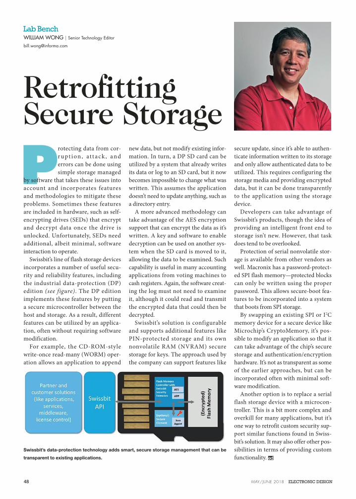
WILLIAM WONG | Senior Technology Editor
Protecting data from cor-
r upt i on , a t t a c k , an d
errors can be done using
simple storage managed
by software that takes these issues into
account and incorporates features
and methodologies to mitigate these
problems. Sometimes these features
are included in hardware, such as self-
encrypting drives (SEDs) that encrypt
and decrypt data once the drive is
unlocked. Unfortunately, SEDs need
additional, albeit minimal, software
interaction to operate.
Swissbit’s line of flash storage devices
incorporates a number of useful secu-
rity and reliability features, including
the industrial data-protection (DP)
edition (see figure). The DP edition
implements these features by putting
a secure microcontroller between the
host and storage. As a result, different
features can be utilized by an applica-
tion, often without requiring software
modification.
For example, the CD-ROM-style
write-once read-many (WORM) oper-
ation allows an application to append
new data, but not modify existing infor-
mation. In turn, a DP SD card can be
utilized by a system that already writes
its data or log to an SD card, but it now
becomes impossible to change what was
written. This assumes the application
doesn’t need to update anything, such as
a directory entry.
A more advanced methodology can
take advantage of the AES encryption
support that can encrypt the data as it’s
written. A key and software to enable
decryption can be used on another sys-
tem when the SD card is moved to it,
allowing the data to be examined. Such
capability is useful in many accounting
applications from voting machines to
cash registers. Again, the software creat-
ing the log must not need to examine
it, although it could read and transmit
the encrypted data that could then be
decrypted.
Swissbit’s solution is configurable
and supports additional features like
PIN-protected storage and its own
nonvolatile RAM (NVRAM) secure
storage for keys. The approach used by
the company can support features like
secure update, since it’s able to authen-
ticate information written to its storage
and only allow authenticated data to be
utilized. This requires configuring the
storage media and providing encrypted
data, but it can be done transparently
to the application using the storage
device.
Developers can take advantage of
Swissbit’s products, though the idea of
providing an intelligent front end to
storage isn’t new. However, that task
does tend to be overlooked.
Protection of serial nonvolatile stor-
age is available from other vendors as
well. Macronix has a password-protect-
ed SPI flash memory—protected blocks
can only be written using the proper
password. This allows secure-boot fea-
tures to be incorporated into a system
that boots from SPI storage.
By swapping an existing SPI or I2C
memory device for a secure device like
Microchip’s CryptoMemory, it’s pos-
sible to modify an application so that it
can take advantage of the chip’s secure
storage and authentication/encryption
hardware. It’s not as transparent as some
of the earlier approaches, but can be
incorporated often with minimal soft-
ware modification.
Another option is to replace a serial
flash storage device with a microcon-
troller. This is a bit more complex and
overkill for many applications, but it’s
one way to retrofit custom security sup-
port similar functions found in Swiss-
bit’s solution. It may also offer other pos-
sibilities in terms of providing custom
functionality.
Lab Bench
Retrofitting Secure Storage
Swissbit’s data-protection technology adds smart, secure storage management that can be
transparent to existing applications.
48 MAY/JUNE 2018 ELECTRONIC DESIGN

DTI’S NEW HIGH VOLTAGE OPTICAL SWITCH
WWW.DEANTECHNOLOGY.COM
+1 (972) 248-7691
OPTIMUM PRICEO POPTICAL SWITCH
www.deantechnology.com
For some time, Dean Technology has been providing custom solutions to cus-
tomers using optical diode technology. We are now moving to make these
custom products a part of our standard product ofering, starting with a 10 kV
optical switch / optocoupler, the OPC10M.
This frst optical device from DTI consists of a central diode with two LED drivers
allowing for variable high voltage output from a low voltage reference input. It
is exceptionally space efcient, and the tight control of production methods
will allow DTI to ofer these parts at prices far better than competitive solutions.
IN STOCK TODAY! Contact us for a quote or to place your order!

BREAKTHROUGHPERFORMANCELT8650S
SILENT SWITCHER®2UNRIVALED EASE-OF-USE
Wide VIN Range: 3.0V-42V
4A Each Channel:• Up to 6A Either Channel
Silent Switcher® 2:• Ultralow EMI on any PCB
• Easy PCB Layout
• Internal Capacitors Reduce
Radiated EMI
• Spread Spectrum Modulation
Ultralow IQ Burst Mode®:• 6.2μA IQ Regulating 12VIN
to 5VOUT1 & 3.3VOUT2
• Output Ripple <10mVP-P
DATA SHEET www.analog.com/LT8650S
FEATURED VIDEO Silent Switcher® 2: Dual 4A per Channel Micropower Step-Down Regulator
www.analog.com/LT8650S-video
LT8609S 3.0 to 42
3.4 to 65
3.4 to 42
3.0 to 42
3.0 to 42
3.4 to 65
3.0 to 18
3.0 to 18
2A/3A Peak
6A/7A Peak
6A/7A Peak
2x2A/3A Peak
2x4A/6A Peak
8A
10A
2x9A
0.8
0.97
0.97
0.8
0.8
0.8
0.8
0.8
200kHz to 2.2MHz
200kHz to 3MHz
200kHz to 3MHz
300kHz to 3MHz
200kHz to 3MHz
200kHz to 3MHz
200kHz to 3MHz
300kHz to 3MHz
2.5
2.5
170
6
6.2
2.5
160
20
3x3 LQFN-16
4x4 LQFN-24
4x4 LQFN-24
3x4 LQFN-20
4x6 LQFN-32
4x6 LQFN-32
4x4 LQFN-24
4x7 LQFN-36
Part Number Frequency IQ (μA) PackageVIN Range (V) IOUT (A) VOUT(MIN) (V)
LT8640S
LT8643S
LT8653S
LT8645S
LT8642S
LT8652S
LT8650S
LT8650S
OUT1
OUT2
Easy PCB Layout
6.2µA IQ 2 x 4A IOUT
200kHz to 3MHz CISPR 25 Class 5
94.4% Efcient at 2MHz