Embed Size (px)
Citation preview

1 Introduction
A satellite positioning system determines aglobal location based on the differencebetween a time on the received signal generat-ed by an onboard satellite clock and a groundreception time; it is thus essential to synchro-nize satellite and ground-based clocks. Time-control equipment (TCE) [1][2] is used to per-form this synchronization. This paperdescribes the digital processing unit of a par-ticular TCE device, referred to as the “TCE-PRO.” The TCE-PRO measures the phase ofvarious signals: the reference signal from aHAC (High Accuracy Clock), the signal trans-mitted from the satellite, a signal receivedfrom the ground, and the instrument delay cal-ibration signal in the in-orbit satellite stationthat is sent from the TCE-RF unit via theHAC, permitting calculation of the amount of
delay in each signal, which in turn enablessynchronization of ground and satellite time.In order to compensate for instrument delay,the circuit is constructed to apply digital pro-cessing at all stages, and signals are digitizedimmediately following input. Frequency con-version and demodulation are also performedvia digital processing.
2 Functions of TCE-PRO
We will first briefly discuss the variousfunctions of the TCE-PRO. Fig.1 shows ablock diagram of the device.- Control of TCE unit (TCE control)
Transmission and reception of data to andfrom the data bus RIM of the main body of thesatellite by RS422 serial transmission; controlof the RF unit and determination of RF unitstatus
KIUCHI Hitoshi et al. 117
3-10-2 On-Board Data Processing Part Time-Compar-ison-Equipment Processing Unit (TCE-PRO)
KIUCHI Hitoshi, IMAE Michito, TAKAHASHI Yasuhiro, GOTOH Tadahiro,
NAKAGAWA Fumimaru, FUJIEDA Miho, and HOSOKAWA Mizuhiko
In satellite positioning systems, such as the Global Positioning System (GPS), the receiv-er’s position is calculated from the measured pseudo-range of the received radio signal.This signal is generated by the satellite based on its on-board atomic clock. Any error in theon-board clock directly affects the pseudo-range. Synchronization between the clocks on-board satellites and clocks on earth is thus indispensable for the development of next-gen-eration systems. The goal of our research is to establish a precise method for comparingthe time between earth and satellite clocks. The time-comparison-equipment processingunit (TCE-PRO) on-board Engineering Test Satellite VIII (ETS VIII) functions as the TCE-con-trol unit; it controls data acquisition as well as digital data processing. It calculates thepseudo-ranges and instrumental delay from the code phases and carrier phases of a com-bined IF signal (the received signal, the transmitted signal, and the delay calibration signal),enabling the time to be synchronized between earth and satellite clocks.
Keywords ETS-VIII, Satellite positioning, Time comparison/transfer, Digital signal processing,Delay lock loop (DLL), Costas loop

118
- Acquisition of observed signal (Sampling &SSB D/C)
The overall TCE-PRO system is based ondigital signal processing in order to eliminateinstrument delay. It is common in frequencyconversion (e.g., DC down-conversion) toplace a filter before a mixer for SSB (singlesideband) conversion; however, circuit size islimited in the available satellite components,precluding the use of an FIR filter or similarcomponent. Therefore, an IRM (Image Rejec-tion Mixer) system was adopted. IRM digitalfrequency conversion is also useful in avoid-ing group-delay frequency errors attributableto the use of SSB filters. Frequency conver-sion was performed in two steps: initial coarseconversion, followed by fine conversion. AnNCO (Numerically Controlled Oscillator), adigital version of a VCO (Voltage ControlledOscillator), was adopted for the local oscilla-tors.- Digital signal processing
Generally, code phase detection entails(among others) delay detection, along withsynchronous or asynchronous delay lock loops(DLL), while carrier phase detection involveselements such as second harmonic generationor the Costas loop. To detect code phase andcarrier phase using the TCE, code trackingfeaturing synchronous DLL was adopted, withcarrier tracking incorporating the Costas loop.Both loops are controlled by a CPU (phasecontrol); an error signal is provided both to thecode tracking (C/A code) NCO and to thelocal oscillator (carrier); this signal is then
used to control the loops. Code phase and thecarrier phase are acquired based on the NCOphase or the error signal phase.
2.1 Control of TCE unitThe basic functions of the control timing
system are as follows.- Command/telemetry management between
control timing system and satellite system(RIM)
- Input/output of status (e.g., lock status) viaparallel I/O; control of the RF unit (TCE-RF)
- C/A code generation based on software-spec-ified SV# for internal satellite processing,independent of the digital signal processingunit
- Timing management
2.2 Acquisition of observed signalThe analog signal from the TCE-RF unit is
sampled at 20.46 Msps. When acquiring theobserved signal, two Doppler components aretaken into consideration: the componentresulting from precise Doppler tracking of thesatellite, and the fixed large Doppler compo-nent acting as a basic component. Although itis possible to compensate for both componentsat once, it is an antithetical concept for NCO,between generating a high-frequency signaland a high-resolution signal at lower frequen-cies; therefore, we adopted a method of dual-stage frequency conversion. The NCO is usedfor the first and second local oscillators. TheTCE-RF has the simultaneous generation ofSIN and COS signals in order to compose anIRM, resulting in SSB conversion. Fig.2 illus-trates the principle behind IRM frequencyconversion with reference to an analog signalconfiguration. In the figure, the first NCOremoves a basic component of the frequency,and the second NCO is used for precise track-ing of the carrier. These local signals functionas an element of the Costas loop describedlater.
2.3 Digital signal processingThe code phase and the carrier phase are
measured using digital signal processing.
Journal of the National Institute of Information and Communications Technology Vol.50 Nos.3/4 2003
Overall block diagramFig.1
2.3.1 Delay lock loop (DLL) for codephase synchronization
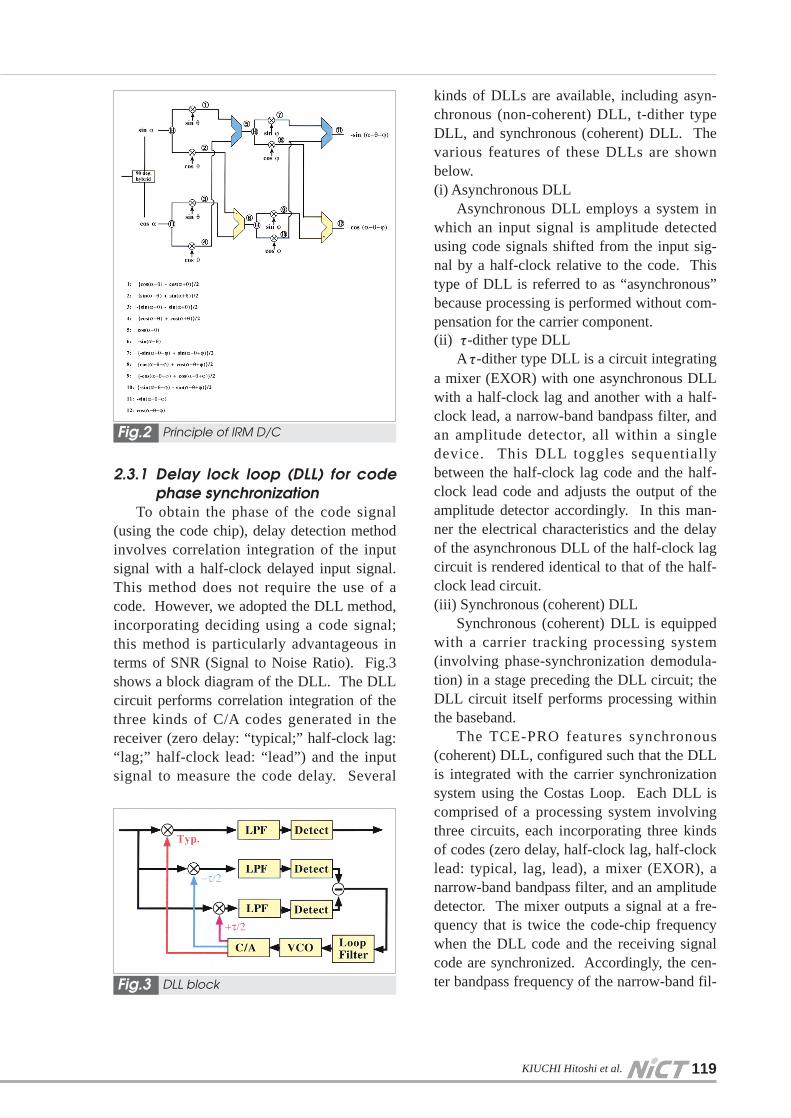
To obtain the phase of the code signal(using the code chip), delay detection methodinvolves correlation integration of the inputsignal with a half-clock delayed input signal.This method does not require the use of acode. However, we adopted the DLL method,incorporating deciding using a code signal;this method is particularly advantageous interms of SNR (Signal to Noise Ratio). Fig.3shows a block diagram of the DLL. The DLLcircuit performs correlation integration of thethree kinds of C/A codes generated in thereceiver (zero delay: “typical;” half-clock lag:“lag;” half-clock lead: “lead”) and the inputsignal to measure the code delay. Several
kinds of DLLs are available, including asyn-chronous (non-coherent) DLL, t-dither typeDLL, and synchronous (coherent) DLL. Thevarious features of these DLLs are shownbelow.(i) Asynchronous DLL
Asynchronous DLL employs a system inwhich an input signal is amplitude detectedusing code signals shifted from the input sig-nal by a half-clock relative to the code. Thistype of DLL is referred to as “asynchronous”because processing is performed without com-pensation for the carrier component.(ii) τ-dither type DLL
Aτ-dither type DLL is a circuit integratinga mixer (EXOR) with one asynchronous DLLwith a half-clock lag and another with a half-clock lead, a narrow-band bandpass filter, andan amplitude detector, all within a singledevice. This DLL toggles sequentiallybetween the half-clock lag code and the half-clock lead code and adjusts the output of theamplitude detector accordingly. In this man-ner the electrical characteristics and the delayof the asynchronous DLL of the half-clock lagcircuit is rendered identical to that of the half-clock lead circuit.(iii) Synchronous (coherent) DLL
Synchronous (coherent) DLL is equippedwith a carrier tracking processing system(involving phase-synchronization demodula-tion) in a stage preceding the DLL circuit; theDLL circuit itself performs processing withinthe baseband.
The TCE-PRO features synchronous(coherent) DLL, configured such that the DLLis integrated with the carrier synchronizationsystem using the Costas Loop. Each DLL iscomprised of a processing system involvingthree circuits, each incorporating three kindsof codes (zero delay, half-clock lag, half-clocklead: typical, lag, lead), a mixer (EXOR), anarrow-band bandpass filter, and an amplitudedetector. The mixer outputs a signal at a fre-quency that is twice the code-chip frequencywhen the DLL code and the receiving signalcode are synchronized. Accordingly, the cen-ter bandpass frequency of the narrow-band fil-
KIUCHI Hitoshi et al. 119
Principle of IRM D/CFig.2
DLL blockFig.3
120
ter (or loop filter) is twice the code-chip fre-quency.
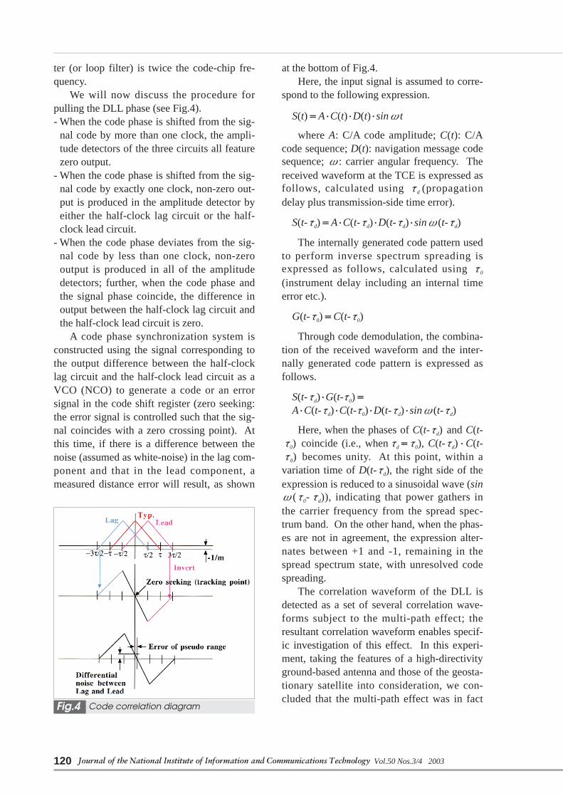
We will now discuss the procedure forpulling the DLL phase (see Fig.4).- When the code phase is shifted from the sig-
nal code by more than one clock, the ampli-tude detectors of the three circuits all featurezero output.
- When the code phase is shifted from the sig-nal code by exactly one clock, non-zero out-put is produced in the amplitude detector byeither the half-clock lag circuit or the half-clock lead circuit.
- When the code phase deviates from the sig-nal code by less than one clock, non-zerooutput is produced in all of the amplitudedetectors; further, when the code phase andthe signal phase coincide, the difference inoutput between the half-clock lag circuit andthe half-clock lead circuit is zero.
A code phase synchronization system isconstructed using the signal corresponding tothe output difference between the half-clocklag circuit and the half-clock lead circuit as aVCO (NCO) to generate a code or an errorsignal in the code shift register (zero seeking:the error signal is controlled such that the sig-nal coincides with a zero crossing point). Atthis time, if there is a difference between thenoise (assumed as white-noise) in the lag com-ponent and that in the lead component, ameasured distance error will result, as shown
at the bottom of Fig.4.Here, the input signal is assumed to corre-
spond to the following expression.
where A: C/A code amplitude; C(t): C/Acode sequence; D(t): navigation message codesequence; ω: carrier angular frequency. Thereceived waveform at the TCE is expressed asfollows, calculated using τd (propagationdelay plus transmission-side time error).
The internally generated code pattern usedto perform inverse spectrum spreading isexpressed as follows, calculated using τ0
(instrument delay including an internal timeerror etc.).
Through code demodulation, the combina-tion of the received waveform and the inter-nally generated code pattern is expressed asfollows.
Here, when the phases of C(t-τd) and C(t-τ0) coincide (i.e., whenτd=τ0), C(t-τd)・C(t-τ0) becomes unity. At this point, within avariation time of D(t-τd), the right side of theexpression is reduced to a sinusoidal wave (sinω(τ0-τd)), indicating that power gathers inthe carrier frequency from the spread spec-trum band. On the other hand, when the phas-es are not in agreement, the expression alter-nates between +1 and -1, remaining in thespread spectrum state, with unresolved codespreading.
The correlation waveform of the DLL isdetected as a set of several correlation wave-forms subject to the multi-path effect; theresultant correlation waveform enables specif-ic investigation of this effect. In this experi-ment, taking the features of a high-directivityground-based antenna and those of the geosta-tionary satellite into consideration, we con-cluded that the multi-path effect was in fact
S(t-τd)・G(t-τ0)=A・C(t-τd)・C(t-τ0)・D(t-τd)・sinω(t-τd)
G(t-τ0)=C(t-τ0)
S(t-τd)=A・C(t-τd)・D(t-τd)・sinω(t-τd)
S(t)=A・C(t)・D(t)・sinωt
Journal of the National Institute of Information and Communications Technology Vol.50 Nos.3/4 2003
Code correlation diagramFig.4
negligible.2.3.2 Costas loop for carrier phase
synchronizationCarrier phase may be determined using a
square-law detection method that does notrequire a code. In addition, the Costas loopmakes use of a PLL (Phase Lock Loop) in amethod of synchronous carrier regenerationthat offers significant advantages in terms ofSNR.
Fig.5 shows a block diagram of the Costasloop.
The input signal is multiplexed (by thefirst and second multipliers, found in themixer) using VCO output signals featuringphases differing from that of the input signalby 90 degrees; the output signals are thenpassed through low pass filters (LPFs) to yieldseparate in-phase and quadrature components(normally referred to as the I and Q compo-nents). These signals are subject to multipli-cation by a third multiplier, and, after removalof the RF component, this output is used asthe control signal of the VCO. With the thirdmultiplexer, even when the signal is code divi-sion multiplexed, signals of the same codewill be multiplied with the same timing, andthus only a carrier phase error will result.
A modulating signal y (t) input into theCostas loop can be expressed as follows.
where A is the baseband signal amplitude,D(t) is the baseband signal, ωc is the carrierangular frequency, and θi is the carrier phase.The VCO outputs two signals whose phases
differ from y(t) by 90 degrees, √2 cos(ωct+θ0)and √2 sin(ωct+θ0) ; these signals are thenmixed with y(t). The RF components of themixed signals are removed with filters toobtain A・D(t)cos(θi-θ0) and A(t)sin(θi-θ0).The error signal of the Costas loop is obtainedas a product of these components.
In this multiplication operation, signals ofthe same codes are multiplied; thus phaseerror proportional to 2(θi-θ0) can be obtainedprovided that (θi-θ0) is sufficiently small. Inother words, phase ambiguity of 180 degreesis present in the reproduced carrier from theCostas Loop. This is due to the feature of themodulation method in which the PSK signalphase is changed by 180 degrees, in otherwords, due to the indeterminacy of the phaseto which the carrier was phase synchronized.
Fig. 6 shows a block diagram whichdemonstrates the above principle.
3 Actual configuration of TCE-PRO
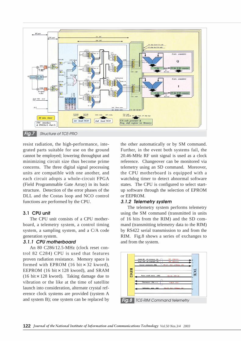
This chapter describes an actual circuitconfiguration. The TCE-PRO is composed ofa CPU (which acquires the control signals andobserved signals of the TCE) and digital sig-nal processing units for transmitted, received,and delay-calibration signals; the equipment isconstructed on a substrate of 240×250 mm.Fig.7 shows a schematic diagram of the over-all configuration. Since the components of theCPU unit and the abovementioned digital sig-nal processing units must all be constructed to
A2・D2(t)───2
sin2(θi-θ0)
y(t)=√2A・D(t)・cos(ωct+θi)
KIUCHI Hitoshi et al. 121
Costas LoopFig.5
Signal processing system block dia-gram
Fig.6
122
resist radiation, the high-performance, inte-grated parts suitable for use on the groundcannot be employed; lowering throughput andminimizing circuit size thus become primeconcerns. The three digital signal processingunits are compatible with one another, andeach circuit adopts a whole-circuit FPGA(Field Programmable Gate Array) in its basicstructure. Detection of the error phases of theDLL and the Costas loop and NCO controlfunctions are performed by the CPU.
3.1 CPU unitThe CPU unit consists of a CPU mother-
board, a telemetry system, a control timingsystem, a sampling system, and a C/A codegeneration system.3.1.1 CPU motherboard
An 80 C286/12.5-MHz (clock reset con-trol 82 C284) CPU is used that featuresproven radiation resistance. Memory space isformed with EPROM (16 bit×32 kword),EEPROM (16 bit×128 kword), and SRAM(16 bit×128 kword). Taking damage due tovibration or the like at the time of satellitelaunch into consideration, alternate crystal ref-erence clock systems are provided (system Aand system B); one system can be replaced by
the other automatically or by SM command.Further, in the event both systems fail, the20.46-MHz RF unit signal is used as a clockreference. Changeover can be monitored viatelemetry using an SD command. Moreover,the CPU motherboard is equipped with awatchdog timer to detect abnormal softwarestates. The CPU is configured to select start-up software through the selection of EPROMor EEPROM.3.1.2 Telemetry system
The telemetry system performs telemetryusing the SM command (transmitted in unitsof 16 bits from the RIM) and the SD com-mand (transmitting telemetry data to the RIM)by RS422 serial transmission to and from theRIM. Fig.8 shows a series of exchanges toand from the system.
Journal of the National Institute of Information and Communications Technology Vol.50 Nos.3/4 2003
Structure of TCE-PROFig.7
TCE-RIM Command telemetryFig.8
3.1.3 Control timing systemThe control timing system is equipped
with a time counter (00 min - 00 sec - 000msec to 59 min - 59 sec - 999 msec), a PP(Parameter Period) cycle counter (0 sec - 000msec to 9 sec - 999 msec), and a 24-bit inter-ruption timer. When a given counter reachesits maximum value, it returns to zero andresumes counting. The PP cycle counter isprogrammed based on milliseconds, makingperiodic interruptions. All counters can bereset by external signals.3.1.4 Sampling system
Analog signals (2.387 MHz ± 1.023 MHz,0 dBm) differing from each other by 90degrees and formed of a mix of transmitted,received, and delay-calibration signals sup-plied from the TCE RF unit, are fed to thesampling system, converted into a digital sig-nal by sampling (1 bit, 20.46 Msps), and sub-sequently supplied to the different signal pro-cessing units. Although loss of coherence dueto 1-bit quantization reaches 36% [3] evenwhen the Nyquist rate is maintained, all of theloss is in amplitude information; there is noloss in phase information. The system isinsensitive to amplitude variation, and is thussuitable for use as a system to acquire timingsignals efficiently, as described in this paper.An anti-aliasing filter is installed in the outputstage of the RF unit (TCE-RF). The digitizedsignal is passed along to the digital signal pro-cessing units (transmitted, received, anddelay-calibration signal processing units) inthe next stage.3.1.5 C/A code generation system
The C/A code generation system generatesa C/A code for demodulation based on theSV# specified by the software. The C/A codeis output in synchronization with a 1.023-MHztiming signal from the CPU unit. This systemshifts 1 bit of the code (and deletes/duplicates1 bit). The system features a 20-bit variableshift register for fine-tuning phase when codesearching, and is capable of adjusting phase ata resolution of 20.46 MHz. The system simul-taneously generates three kinds of phasecodes: “typical,” “1/2-bit lead,” and “1/2-bit
lag” for the DLL circuit.
3.2 Digital signal processing unit(transmitted, received, and delay-calibration signal processing units)
The digital signal processing units (fortransmitted, received, and delay-calibrationsignals) perform simultaneous measurementof the signal transmitted from the satellite, asignal received from the ground, the code ofthe satellite instrument delay calibration sig-nal, and the carrier phase, based on a timingsignal from the CPU unit. Measurementresults are read by the CPU unit, processed,and output by telemetry.3.2.1 Digital down converter
Since available CPUs and FPGAs featur-ing sufficient radiation resistance fall consid-erably short in terms of performance, weadopted the IRM method (rather than the ini-tially envisioned SSB method, which entailedthe use of FIR filters).
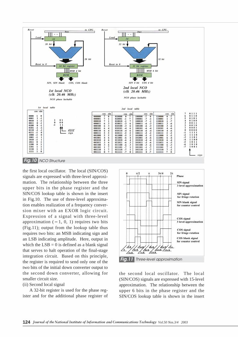
The NCO consists of a phase register (Φ),an additional phase register (ΔΦ), an adder,and a SIN/COS look-up table. Fig.10 showsthe relevant block diagram. All bits of thephase resister are used to express phases of0–360 degrees. ΔΦis controlled by the PPclock; a value of ΔΦ(corresponding to thelocal frequency) is added to F every 1.023-MHz clock increment. An amplitude corre-sponding to this phase is read from theSIN/COS look-up table and is output. Thevalue of the phase register is latched for eachPP and rendered readable.(i) First local signal
24-bit registers are used for the phase reg-ister and for the additional phase register of
KIUCHI Hitoshi et al. 123
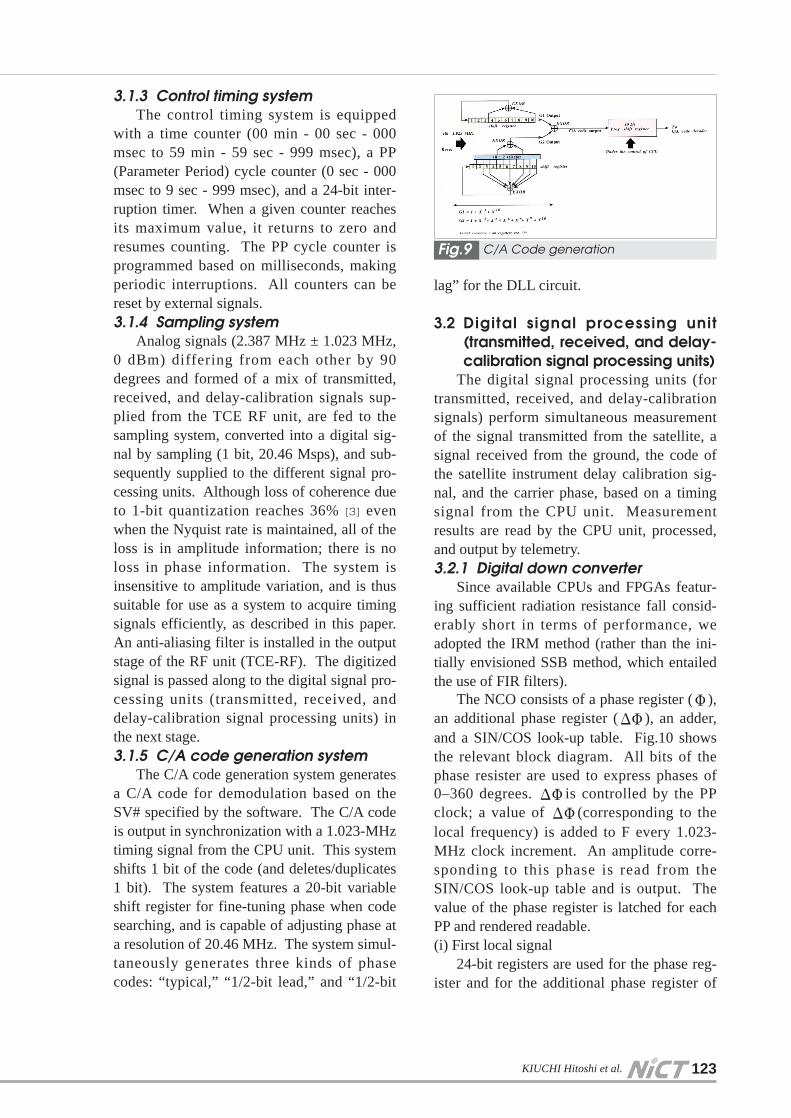
C/A Code generationFig.9
124
the first local oscillator. The local (SIN/COS)signals are expressed with three-level approxi-mation. The relationship between the threeupper bits in the phase register and theSIN/COS lookup table is shown in the insertin Fig.10. The use of three-level approxima-tion enables realization of a frequency conver-sion mixer with an EXOR logic circuit.Expression of a signal with three-levelapproximation (-1, 0, 1) requires two bits(Fig.11); output from the lookup table thusrequires two bits: an MSB indicating sign andan LSB indicating amplitude. Here, output inwhich the LSB = 0 is defined as a blank signalthat serves to halt operation of the final-stageintegration circuit. Based on this principle,the register is required to send only one of thetwo bits of the initial down converter output tothe second down converter, allowing forsmaller circuit size.(ii) Second local signal
A 32-bit register is used for the phase reg-ister and for the additional phase register of
the second local oscillator. The local(SIN/COS) signals are expressed with 15-levelapproximation. The relationship between theupper 6 bits in the phase register and theSIN/COS lookup table is shown in the insert
Journal of the National Institute of Information and Communications Technology Vol.50 Nos.3/4 2003
NCO StructureFig.10
Three-level approximationFig.11

in Fig.10.In this system, the down converter can be
changed to an up converter by changing thesign at one position, as is clear from the prin-ciple illustrated in Fig.2. Fig.12 shows theresults of simulation for a case in which thefrequency ratio (original signal to first localsignal to second local signal) is set at512:500:5 in the digital IRM. As indicated,the signals employed consist of the originalsignal (1 bit - 2 levels), the first local signal (2bits - 3 levels), and the second local signal (4bits - 15 levels). The upper two diagramsshow the results of first-stage IRM frequencyconversion (I: in-phase component, Q: quadra-ture component), with three-level output. Thelower two diagrams show the results of sec-ond-stage IRM frequency conversion simula-tion at a frequency at which aliasing is likelyto produce multiple images. In the figure, animage frequency component featuring a lowlevel is anticipated at low frequencies. Inprinciple it is best to pass the signal through afew taps of FIR filters downstream from thedigital IRM.
3.2.2 Dual-correlation integrationcounter
The dual-correlation integration counterconsists of a 24-bit up/down counter. Coun-ters for the SIN component and for the COScomponent are prepared for each of threekinds of data: “typical,” “1/2-bit lead,” and“1/2-bit lag.” The up/down counter is con-trolled using 5-bit MSB code bits generated bydemodulation (i.e., through correlation opera-tion). This value is latched for each integra-tion time and is read by the CPU. Once thisvalue is fixed, the counter will be reset. Thus,phase difference can be arrived at by calculat-ing the ATAN components using the SIN com-ponents and the COS components of the I andQ components of “typical.” This enables thesame operations performed on the third multi-plier of the Costa loop to be performed on theCPU.
Each of these circuits can support bothsynchronous and asynchronous operation; thespecific method to be supported is determinedthrough operational analysis. Moreover, theability to rewrite the control software andFPGA software from the ground has also beenconsidered.
KIUCHI Hitoshi et al. 125
IRM simulation diagramFig.12
126
4 Acknowledgement
We are thankful to Mr. Hiroshima of the
COSMO RESEARCH Corp., who manufac-tured the equipment used in the course of thisresearch.
Journal of the National Institute of Information and Communications Technology Vol.50 Nos.3/4 2003
References1 Y. Takahashi, "3-10-1 RF Part", This Special Issue of NICT Journal.
2 Y. Takahashi, M. Imae, H. Kiuchi, M. Hosokawa, M. Aida, T. Gotoh, H. Noda, S. Hama, and S. Kozono,
"Experimental plan for time comparison equipment for ETS-VIII satellite," IEICE trans. B, Vol. J84-B, No.12,
pp.2101-2107, 2001.12.
3 J.H.VanVleck and D.Middleton, "The spectrum of clipped noise", Proc. IEEE, Vol.54, No.1, pp.2-19, 1966.
KIUCHI Hitoshi, Dr. Eng.
Senior Researcher, Optical SpaceCommunications Group, WirelessCommunications Division
Radio Interferometry, Optical SpaceCommunication
TAKAHASHI Yasuhiro
Senior Researcher, Time and Frequen-cy Measurements Group, AppliedResearch and Standards Division
Satellite Communication, SatellitePositioning System
IMAE Michito
Leader, Time and Frequency Measure-ments Group, Applied Research andStandards Division (present NationalInstitute of Advanced Industrial Scienceand Technology)
Frequency Standard, especially on Pre-cise Time Transfer
GOTOH Tadahiro
Researcher, Time and Frequency Mea-surements Group, Applied Researchand Standards Division
GPS Time Transfer
NAKAGAWA Fumimaru, Ph. D.
Research Fellow, Time and FrequencyMeasurements Group, AppliedResearch and Standards Division
Satellite Navigation, Satellite TimeTransfer
FUJIEDA Miho, Ph. D.
Research Fellow, Time and FrequencyMeasurements Group, AppliedResearch and Standards Division
Time Transfer, Satellite Navigation
HOSOKAWA Mizuhiko, Ph. D.
Leader, Atomic Frequency StandardsGroup, Applied Research and Stan-dards Division
Atomic Frequency Standards, SpaceTime Measurements


![Comparative phylogeography in rainforest trees from lower ... › uploads › tx_news › Compar… · graphic pattern in South American forest organisms [12], in European Alpine](https://img.pdfslide.us/doc/110x75/60d023727669cc735e4a8685/comparative-phylogeography-in-rainforest-trees-from-lower-a-uploads-a-txnews.jpg)