Embed Size (px)
Citation preview
271
Nanoimprint9. Nanoimprint Lithography –Patterning of Resists Using Molding
Helmut Schift, Anders Kristensen
Nanoimprint lithography (NIL) is an emerginghigh-resolution parallel patterning method,mainly aimed towards fields in which electron-beam and high-end photolithography are costlyand do not provide sufficient resolution at rea-sonable throughput. In a top-down approach,a surface pattern of a stamp is replicated intoa material by mechanical contact and three-dimensional material displacement. This can bedone by shaping a liquid followed by a curingprocess for hardening, by variation of the ther-momechanical properties of a film by heatingand cooling, or by any other kind of shaping pro-cess using the difference in hardness of a moldand a moldable material. The local thickness con-trast of the resulting thin molded film can beused as a means to pattern an underlying sub-strate at the wafer level by standard patterntransfer methods, but also directly in applicationswhere a bulk modified functional layer is needed.This makes NIL a promising technique for volumemanufacture of nanostructured components. Atpresent, structures with feature sizes down to 5 nmhave been realized, and the resolution is limitedby the ability to manufacture the stamp relief.For historical reasons, the term nanoimprintlithography refers to a hot embossing process(thermal NIL). In ultraviolet (UV)-NIL, a pho-topolymerizable resin is used together witha UV-transparent stamp. In both processes thin-film squeeze flow and capillary action playa central role in understanding the NIL pro-cess. In this chapter we will give an overviewof NIL, with emphasis on general principlesand concepts rather than specific process is-sues and state-of-the-art tools and processes.Material aspects of stamps and resists are dis-cussed. We discuss specific applications whereimprint methods have significant advantages over
9.1 Emerging Nanopatterning Methods........ 2739.1.1 Next-Generation Lithography ........ 2749.1.2 Variants
of Nanoimprint Lithography .......... 275
9.2 Nanoimprint Process ............................. 2779.2.1 Limits of Molding ......................... 2779.2.2 Squeeze Flow of Thin Films............ 2799.2.3 Residual Layer Thickness
Homogeneity ............................... 2819.2.4 Demolding .................................. 2829.2.5 Curing of Resists........................... 2839.2.6 Pattern Transfer ........................... 2839.2.7 Mix-and-Match Methods .............. 2859.2.8 Multilayer and Multilevel Systems .. 2869.2.9 Reversal NIL ................................. 287
9.3 Tools and Materials for Nanoimprinting . 2889.3.1 Resist Materials for Nanoimprinting 2889.3.2 Stamp Materials ........................... 2909.3.3 Stamp Fabrication ........................ 2909.3.4 Antiadhesive Coatings................... 2919.3.5 Imprinting Machines .................... 292
9.4 Nanoimprinting Applications ................. 2949.4.1 Types of Nanoimprinting
Applications ................................ 2949.4.2 Patterned Magnetic Media
for Hard-Disk Drives ..................... 2959.4.3 Subwavelength Metal-Strip
Gratings ...................................... 2979.4.4 High-Brightness Light-Emitting
Diodes ........................................ 2989.4.5 Polymer Optics ............................. 2999.4.6 Bio Applications ........................... 300
9.5 Conclusions and Outlook ....................... 302
References .................................................. 304
other structuring methods. We conclude by dis-cussing areas where further development in thisfield is required.
PartA
9
272 Part A Nanostructures, Micro-/Nanofabrication and Materials
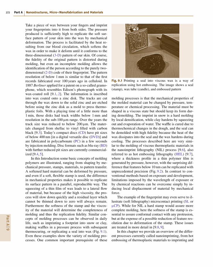
Take a piece of wax between your fingers and imprintyour fingerprints into it from both sides. The pressureproduced is sufficiently high to replicate the soft sur-face pattern of your skin into the wax by mechanicaldeformation. The process is facilitated by the heat re-sulting from our blood circulation, which softens thewax in order to make it deform until it conforms to thethree-dimensional (3-D) pattern of our skin. Of course,the fidelity of the original pattern is distorted duringmolding, but even an incomplete molding allows theidentification of the person according to the purely two-dimensional (2-D) code of their fingerprint. The patternresolution of below 1 mm is similar to that of the firstrecords fabricated over 100 years ago in celluloid. In1887 Berliner applied for a patent on a so-called gramo-phone, which resembles Edison’s phonograph with itswax-coated roll [9.1, 2]. The information is inscribedinto wax coated onto a zinc disk. The tracks are cutthrough the wax down to the solid zinc and are etchedbefore using the zinc disk as a mold to press thermo-plastic foils. With a playing time of a little more than1 min, those disks had track widths below 1 mm andresolution in the sub-100 μm range. Over the years thetrack size was reduced to below 200 μm. The mater-ials changed from shellac to vinyl filled with carbonblack [9.3]. Today’s compact discs (CD) have pit sizesof below 400 nm [in a digital versatile disc (DVD)] andare fabricated in polycarbonate (PC) in a few secondsby injection molding. Disc formats such as blu-ray (BD)with further reduced pit sizes are currently commercial-ized [9.4, 5].
In this Introduction some basic concepts of moldingpolymers are illustrated, ranging from shaping by me-chanical pressure, stamps, materials, to pattern transfer.A softened hard material can be deformed by pressure,and even if a soft, flexible stamp is used, the differencein mechanical properties makes it possible to replicateits surface pattern in a parallel, reproducible way. Thesqueezing of a thin film of wax leads to a lateral flowof material, but because of the high viscosity, the pro-cess will slow down quickly and a residual layer whichcannot be thinned down to zero will always remain.Furthermore the softness of the stamp and the viscos-ity of the material will determine the completeness ofmolding and thus the replication fidelity. Similar con-cepts of molding processes can be observed in dailylife, such as imprinting a footprint into snow or clay,making waffles in a pressure process with subsequentthermocuring, or replicating a seal into wax (Fig. 9.1).Even these examples show the variety of molding pro-cesses. One common important prerequisite of these
Fig. 9.1 Printing a seal into viscous wax is a way ofreplication using hot embossing. The image shows a seal(stamp), wax tube (candle), and embossed pattern
molding processes is that the mechanical properties ofthe molded material can be changed by pressure, tem-perature or chemical processing. The material must beshaped in a viscous state but should keep its form dur-ing demolding. The imprint in snow is a hard moldingby local densification, while clay hardens by squeezingout and evaporation of water. The waffle is cured due tothermochemical changes in the dough, and the seal canbe demolded with high fidelity because the heat of thewax dissipates into the seal and the wax hardens duringcooling. The processes described here are very simi-lar to the molding of viscous thermoplastic materials inthe nanoimprint lithography (NIL) process [9.6], alsoreferred to as hot embossing lithography (HEL) [9.7],where a thickness profile in a thin polymer film isgenerated by pressure, however, with the surprising dif-ference that features below 10 nm can be replicated withunprecedented precision (Fig. 9.2). In contrast to con-ventional methods based on exposure and development,limitations imposed by the wavelength of exposure orby chemical reactions can be overcome simply by in-ducing local displacement of material by mechanicalforce.
The example of the fingerprint may even serve to il-lustrate (soft lithography) microcontact printing (SL orμCP). While for NIL a hard stamp would assure morecomplete molding, here the softness of the stamp is es-sential to assure conformal contact with any protrusion,but at the expense of a possible reduction of feature res-olution due to deformation of the stamp. These issuesare treated in more detail in [9.8, 9].
In this chapter we provide an overview of the differ-ent processes currently called nanoimprinting, from hotembossing of thermoplastic materials to imprinting and
PartA
9

Nanoimprint Lithography – Patterning of Resists Using Molding 9.1 Emerging Nanopatterning Methods 273
a) b) c)10 nm 10 nm
40 nm
10 nmFig. 9.2a–c Micrographs showingthe basic steps of NIL, demonstratedby Chou and Krauss [9.6]. (a) NILstamp in silicon with a 40 nm-periodarray of pillars with 40 nm height,(b) imprinted 10 nm-diameter holesin a thin polymer film (PMMA),(c) 10 nm metal dots after patterntransfer (lift-off), using the thinpolymer layer as a mask
curing of liquid resins. After this Introduction into thebasics of molding, Sect. 9.1 places the two main NILtechniques into the context of the emerging nanopat-terning methods for lithography. Section 9.2 is the mainsection, where the NIL process is described in detail,beginning with a discussion about polymer properties,giving an insight into squeeze flow of thin films. Asa first step towards applications major pattern trans-fer techniques used in NIL are presented. Section 9.3presents materials and tools for NIL, ranging frommaterials for stamps and resists, to imprint machines.Section 9.4 presents typical applications which are cur-rently envisaged both at an industrial and at laboratoryscale. Although for many people the main driving forcebehind NIL is its use as next-generation lithography(NGL) for complementary metal–oxide–semiconductor(CMOS) chip fabrication, the reader will be introducedto different other applications which do not have thedemanding overlay requirements imposed by multilevel
processes. We conclude with an outlook in Sect. 9.5, inwhich we discuss the prospects of NIL and aspects ofits commercialization. Further information can be foundin the references, in publications dealing with so-calledlithography, electroforming, and molding (LIGA, fromits German abbreviation) technology [9.10] and opticalstorage fabrication, but not least within this Handbookin Chaps. 8 and 10 about silicon micromachining andsoft lithography. In this chapter we restrict ourselves tolithographic patterning of thin films on hard substrates.We present basic concepts rather than state-of-the-arttools and hot scientific issues. As a complement to thischapter, the reader is advised to refer to two publica-tions: A recent review on NIL [9.11] deals with a rangeof process issues relevant for research and industry, anda deeper insight into advanced concepts of printing.Specific NIL processes and process flows for a vari-ety of applications are presented in the NaPa Libraryof processes (NaPa LoP) [9.12].
9.1 Emerging Nanopatterning Methods
Nanoimprint lithography (NIL) is a replication tech-nique which has proven to provide a resolution un-matched by many other techniques, while at the sametime offering parallel and fast fabrication of micro- andnanostructures [9.13]. On the one hand, this enablesits application to fields where large areas covered bynanostructures or a number of identical structures forstatistical evaluation are needed. This was often impos-sible due to the low throughput of lithographic researchtools. On the other hand the resolution achieved sofar by molding is much higher than that used in in-dustrial fabrication of processors and memory chipswith high-end photolithography (PL). This makes NILa promising technology for NGL [9.14]. Apart fromthese advantages molding offers more: By creatinga three-dimensional (3-D) resist pattern by mechani-
cal displacement of material, the patterning of a rangeof specific functional materials and polymers becomespossible, without loss of their chemical properties dur-ing molding. Furthermore this ability can be used tofabricate complex structures, e.g., by building up de-vices with embedded channels. These processes arepresented in more detail in Sect. 9.2.
In this section we present the basic concepts of NILand how it can conform to the requirements of state-of-the-art nanofabrication techniques. NIL uses, as doother lithographic techniques, the concept of resist pat-terning (which can also be found in different chaptersin this Handbook). The resist patterns are generated bymolding of a viscous material and fixed by cooling andcuring, while in PL the resist is patterned by selective lo-cal chemical modification of a positive or negative resist
PartA
9.1
274 Part A Nanostructures, Micro-/Nanofabrication and Materials
Viscous polymer
Crosslinked
Expose throughstamp
polymer
Hard stampTransparentLiquid resin
b)a)
Hard stamp
Solid polymerSubstrate
Solid polymer
Hot embossing
Tg
0.5 barTg
Tg
Tg
UV-NIL
Tg
80Gap
bar
Fig. 9.3a,b Schematic of NIL process: (a) thermal NIL (hot embossing) and (b) UV-NIL. In both cases a thickness profileis generated in the thin polymer layer. After removing the residual layer, the remaining polymer can serve as a maskinglayer which can be used as a resist for pattern transfer
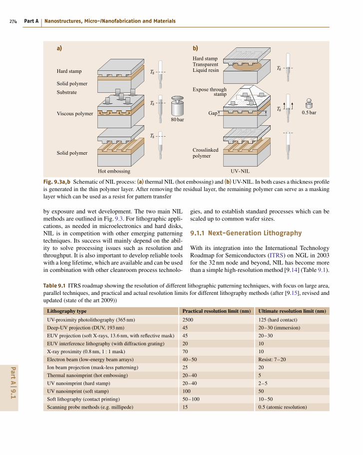
by exposure and wet development. The two main NILmethods are outlined in Fig. 9.3. For lithographic appli-cations, as needed in microelectronics and hard disks,NIL is in competition with other emerging patterningtechniques. Its success will mainly depend on the abil-ity to solve processing issues such as resolution andthroughput. It is also important to develop reliable toolswith a long lifetime, which are available and can be usedin combination with other cleanroom process technolo-
Table 9.1 ITRS roadmap showing the resolution of different lithographic patterning techniques, with focus on large area,parallel techniques, and practical and actual resolution limits for different lithography methods (after [9.15], revised andupdated (state of the art 2009))
Lithography type Practical resolution limit (nm) Ultimate resolution limit (nm)
UV-proximity photolithography (365 nm) 2500 125 (hard contact)
Deep-UV projection (DUV, 193 nm) 45 20–30 (immersion)
EUV projection (soft X-rays, 13.6 nm, with reflective mask) 45 20–30
EUV interference lithography (with diffraction grating) 20 10
X-ray proximity (0.8 nm, 1 : 1 mask) 70 10
Electron beam (low-energy beam arrays) 40–50 Resist: 7–20
Ion beam projection (mask-less patterning) 25 20
Thermal nanoimprint (hot embossing) 20–40 5
UV nanoimprint (hard stamp) 20–40 2–5
UV nanoimprint (soft stamp) 100 50
Soft lithography (contact printing) 50–100 10–50
Scanning probe methods (e.g. millipede) 15 0.5 (atomic resolution)
gies, and to establish standard processes which can bescaled up to common wafer sizes.
9.1.1 Next-Generation Lithography
With its integration into the International TechnologyRoadmap for Semiconductors (ITRS) on NGL in 2003for the 32 nm node and beyond, NIL has become morethan a simple high-resolution method [9.14] (Table 9.1).
PartA
9.1
Nanoimprint Lithography – Patterning of Resists Using Molding 9.1 Emerging Nanopatterning Methods 275
It is now considered a candidate for replacing or com-plementing advanced optical lithographic methods forthe fabrication of processors and solid-state memorychips, which over the years have been developed andpushed to higher resolution with a vast investment ofresources. Over more than 40 years, Moore’s law hasdescribed with amazing accuracy the reduction of fea-ture size (and cost per transistor), and therefore servesas a roadmap for the developments needed for futuremicrochips [9.15–17]. This development is driven byeconomic considerations, and leads to competition be-tween different candidate fabrication methods. These donot only have to provide the resolution of the smallestfeature size (node), but also satisfy issues such as align-ment (overlay of several masking levels), critical dimen-sions (CD), simple mask fabrication, high throughput(mass fabrication), and low cost of ownership (CoO,e.g. no dependence of expensive machines such as syn-chrotrons, back-ups and tool and mask redundancy),which become increasingly difficult to meet if smallerexposure wavelengths have to be used (Fig. 9.4).
The financial and physical barriers to these tech-niques are now so great that alternatives such as NILare considered as a way out of this spiral of rising in-vestments for next-generation chips with even smallerfeature sizes. This means that all technical issues con-nected with NIL for integration into chip manufacturing
10Resolution (nm)
1000
Exposure rate (cm2/s)
100
102
101
100
10–1
10–2
10–3
10–4
10–5
ArF(193nm)F2
(157nm) DUV
KrF(248nm) i-line (365nm)
g-line (436nm)PL
EUV(13.6nm)
UV-NIL
T-NIL NILSinglepointEBL
SPM
Celle-beam
X-ray
Ionbeam
Largearea
Fig. 9.4 Comparison of exposure rate and resolution ofdifferent lithographic techniques. To date, NIL providesa high resolution of below 10 nm, and achieves wafer-scale patterning within some minutes down to seconds(after [9.15])
must satisfy the requirements for full compatibility,similar specifications, yield, and throughput. The in-vestments are expected to be lower than for the currentfrontrunners: extreme-ultraviolet (EUV) lithography orparallel electron-beam exposure.
9.1.2 Variants of Nanoimprint Lithography
Molding of Thermoplastic Resistsby Thermal NIL
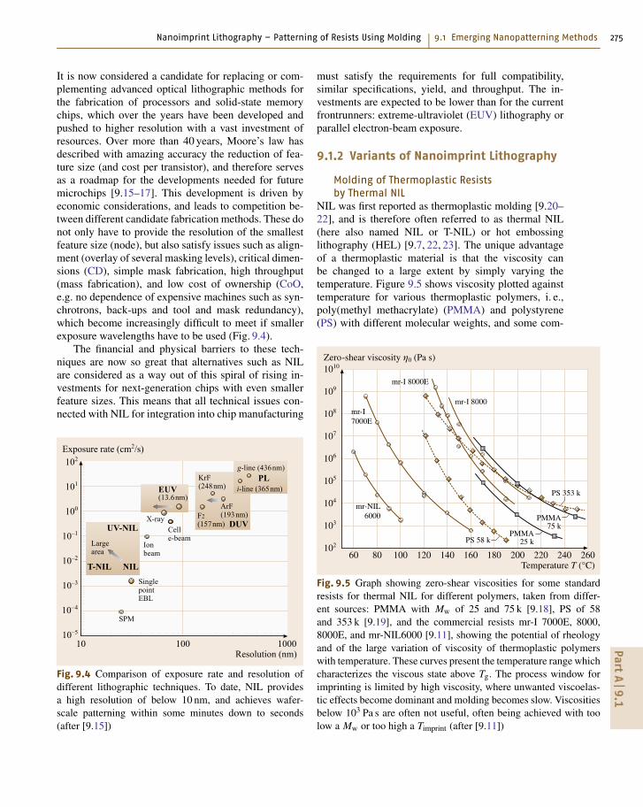
NIL was first reported as thermoplastic molding [9.20–22], and is therefore often referred to as thermal NIL(here also named NIL or T-NIL) or hot embossinglithography (HEL) [9.7, 22, 23]. The unique advantageof a thermoplastic material is that the viscosity canbe changed to a large extent by simply varying thetemperature. Figure 9.5 shows viscosity plotted againsttemperature for various thermoplastic polymers, i. e.,poly(methyl methacrylate) (PMMA) and polystyrene(PS) with different molecular weights, and some com-
60 80 100 120 140 160 180 200
PMMA25 k
PMMA75 k
PS 353 k
mr-I 8000
mr-I 8000E
mr-I7000E
mr-NIL6000
PS 58 k
220 240 260
Zero-shear viscosity η0 (Pa s)
Temperature T (°C)
1010
109
108
107
106
105
104
103
102
Fig. 9.5 Graph showing zero-shear viscosities for some standardresists for thermal NIL for different polymers, taken from differ-ent sources: PMMA with Mw of 25 and 75 k [9.18], PS of 58and 353 k [9.19], and the commercial resists mr-I 7000E, 8000,8000E, and mr-NIL6000 [9.11], showing the potential of rheologyand of the large variation of viscosity of thermoplastic polymerswith temperature. These curves present the temperature range whichcharacterizes the viscous state above Tg. The process window forimprinting is limited by high viscosity, where unwanted viscoelas-tic effects become dominant and molding becomes slow. Viscositiesbelow 103 Pa s are often not useful, often being achieved with toolow a Mw or too high a Timprint (after [9.11])
PartA
9.1
276 Part A Nanostructures, Micro-/Nanofabrication and Materials
0 Time
Molding
Temperature
Tg
1
Viscous
Solid
2 3Thermocuring
4 5UV postcuring Pressure
0
Timprint
Pimprint
Tdemold
20°C
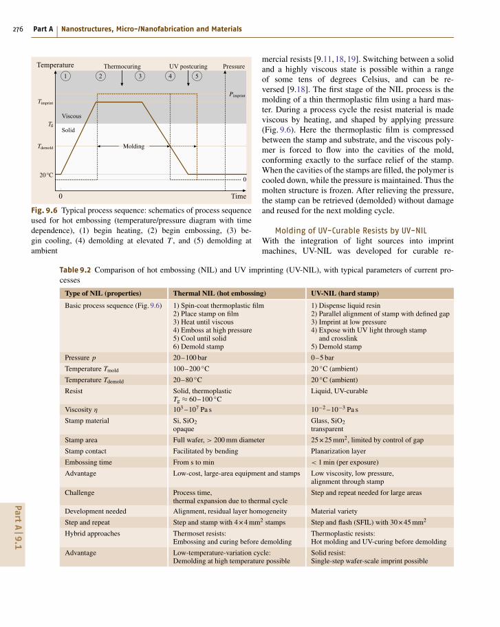
Fig. 9.6 Typical process sequence: schematics of process sequenceused for hot embossing (temperature/pressure diagram with timedependence), (1) begin heating, (2) begin embossing, (3) be-gin cooling, (4) demolding at elevated T , and (5) demolding atambient
Table 9.2 Comparison of hot embossing (NIL) and UV imprinting (UV-NIL), with typical parameters of current pro-cesses
Type of NIL (properties) Thermal NIL (hot embossing) UV-NIL (hard stamp)
Basic process sequence (Fig. 9.6) 1) Spin-coat thermoplastic film2) Place stamp on film3) Heat until viscous4) Emboss at high pressure5) Cool until solid6) Demold stamp
1) Dispense liquid resin2) Parallel alignment of stamp with defined gap3) Imprint at low pressure4) Expose with UV light through stamp
and crosslink5) Demold stamp
Pressure p 20–100 bar 0–5 bar
Temperature Tmold 100–200 ◦C 20 ◦C (ambient)
Temperature Tdemold 20–80 ◦C 20 ◦C (ambient)
Resist Solid, thermoplasticTg ≈ 60–100 ◦C
Liquid, UV-curable
Viscosity η 103 –107 Pa s 10−2 –10−3 Pa s
Stamp material Si, SiO2opaque
Glass, SiO2transparent
Stamp area Full wafer, > 200 mm diameter 25 × 25 mm2, limited by control of gap
Stamp contact Facilitated by bending Planarization layer
Embossing time From s to min < 1 min (per exposure)
Advantage Low-cost, large-area equipment and stamps Low viscosity, low pressure,alignment through stamp
Challenge Process time,thermal expansion due to thermal cycle
Step and repeat needed for large areas
Development needed Alignment, residual layer homogeneity Material variety
Step and repeat Step and stamp with 4 × 4 mm2 stamps Step and flash (SFIL) with 30 × 45 mm2
Hybrid approaches Thermoset resists:Embossing and curing before demolding
Thermoplastic resists:Hot molding and UV-curing before demolding
Advantage Low-temperature-variation cycle:Demolding at high temperature possible
Solid resist:Single-step wafer-scale imprint possible
mercial resists [9.11,18,19]. Switching between a solidand a highly viscous state is possible within a rangeof some tens of degrees Celsius, and can be re-versed [9.18]. The first stage of the NIL process is themolding of a thin thermoplastic film using a hard mas-ter. During a process cycle the resist material is madeviscous by heating, and shaped by applying pressure(Fig. 9.6). Here the thermoplastic film is compressedbetween the stamp and substrate, and the viscous poly-mer is forced to flow into the cavities of the mold,conforming exactly to the surface relief of the stamp.When the cavities of the stamps are filled, the polymer iscooled down, while the pressure is maintained. Thus themolten structure is frozen. After relieving the pressure,the stamp can be retrieved (demolded) without damageand reused for the next molding cycle.
Molding of UV-Curable Resists by UV-NILWith the integration of light sources into imprintmachines, UV-NIL was developed for curable re-
PartA
9.1

Nanoimprint Lithography – Patterning of Resists Using Molding 9.2 Nanoimprint Process 277
sists [9.24–27]. The basic difference between UV-NILand NIL is that a resin that is liquid at room tem-perature is shaped by a moderate pressure, and byexposing light through the transparent stamp the resinis cross-linked and hardened. The stamp either sinksdown to the substrate or must be kept at a constantdistance from the substrate during both filling and ex-posure, due to the low resist viscosities. The mechanicalsetup has to be able to compensate for wedge errorsin a low-imprint-pressure process. Patterning on nonflatsubstrates or over topography therefore requires a pla-narization strategy and often small stamps. Because ofthe small pressures used, both hard stamps or stampswith protrusions made by soft material on a rigid back-bone can be used.
Resist Window Opening for Pattern TransferA basic characteristic of NIL is the patterning of a thinlayer of material, in which the dimensions (lateralstructure size and height) become similar to the film
thickness used. In a second step, the thickness profileof the polymer film can now be used as a resist for pat-tern transfer. For this, the residual layer remaining inthe thin areas of the resist has to be removed, which isdone by homogeneously thinning down the entire re-sist using an (ideally) anisotropic etching process. Inthis way, process windows are opened to the substrateand the polymer can be used as a masking layer for fur-ther processing steps. There are an increasing numberof process variations, which are mostly variants of theestablished thermal NIL and UV-NIL processes, partic-ularly those using special methods of pattern transfer(e.g., reversal imprint) and hybrid processes (combi-nations of different processes). All the processes havetheir specific advantages, e.g., while UV-NIL can beperformed at room temperature, hot embossing is lowcost since nontransparent stamps can be used. The ma-jor characteristics of typical processes, along with thoseof hybrid approaches, are summarized in Table 9.2 andpresented in more detail in [9.11].
9.2 Nanoimprint Process
Molding techniques based on imprint processes makeuse of the differences between the mechanical prop-erties of a structured stamp and a molding material.The viscous molding material is shaped by pressing thehard stamp into it until the polymer conforms to thestamp surface. In hot embossing processes we mostlydeal with thermoplastic materials whose mechanicalproperties can be repeatedly and reversibly changedfrom a solid into a viscous state by simply varyingthe temperature. In order to achieve a reasonable pro-cess time and yield, this is normally carried out underhigh pressure. Thermal NIL deals with a viscosity rangewhich is considered as sufficiently low to enable sig-nificant squeeze flow over large distances, but highenough that bending of wafers can be used to equi-librate surface undulations of common substrates andpattern density variations in stamps. The rheologicalprocesses described here for thermoplastic materialscan be considered to be similar for thermoset or UV-curable materials as long as the thermomechanicalproperties can be changed without affecting the chem-ical ones. While squeeze flow governs high-viscositymolding (where pressure is the driving force to displacethe viscous material), in UV-NIL low pressure or evenmold filling by simple capillary action (where surfaceenergy controls the wetting and spreading of the vis-
cous material) is possible if very low-viscosity resinsare used. In this section we want to take a closer look atthe squeeze flow of thin polymer films as used for ther-mal NIL, a concept which is quite general and enablesan insight into possible parameter variations for processoptimization. We will give a brief introduction to thetheory of polymers [9.28, 29] and discuss the implica-tions for NIL. This will enable the reader to understandrheology in NIL from a practical point of view. Morefundamental questions of squeeze flow are discussedin [9.30, 31]. We conclude this section by presentingpattern transfer processes used in combination with NILand show examples of the fabrication of simple devices.In the section on curable resists, we will introduce con-cepts mainly used in UV-NIL such as soft UV-NIL anddroplet dispensing.
9.2.1 Limits of Molding
Resists used in NIL are polymers, which are definedby their chemical composition and physical proper-ties. In the case of molding these are often long-chainmolecules with molecular weight Mw. The polymerMw is important because it determines many physicalproperties. Some examples include the temperatures fortransitions from liquid to viscoelastic rubber to solid,
PartA
9.2

278 Part A Nanostructures, Micro-/Nanofabrication and Materials
and mechanical properties such as stiffness, strength,viscoelasticity, toughness, and viscosity. However, if theMw is too low, the transition temperatures will be toolow and the mechanical properties of the polymer ma-terial will be insufficient to be useful as a hard resist forpattern transfer. The examples given in this section aresimple and meant to illustrate the specific terms neededto understand polymer behavior in molding.
It has been known for a long time that polymerscan replicate topographies with high fidelity. Up to now5 nm resolution of polymer ridges with a pitch of 14 nmhas been demonstrated [9.32]. In contrast with meth-ods such as electron-beam lithography (EBL), wherenanoscale chemical contrast can be produced by lo-cal irradiation-induced chain scission, polymer chainsare only moved and deformed during molding, thus re-taining their chemical properties such as Mw. Moldingtopographic details down to a few nanometers meansthat single polymer chains have to deform or flow. Thisdeformation can be illustrated by comparing the poly-mer with a pot full of cooked spaghetti, and insteadof the viscosity change with temperature we simplytake the different mobility of the filaments when wetor dry. When a water glass, representing the 10 nm pil-lar stamp shown in Fig. 9.2a, is pressed into this pot,single spaghetti filaments have to be moved before theglass can sink into the entangled network. If the poly-mers can slide along each other, the deformation canbe permanent after drying and demolding. If stress isfrozen, the matrix around the cylindrical hole will re-lax after demolding. Note that this simple example canalso be used to illustrate the difference between totallyamorphous and semicrystalline polymers.
A polymer is a large molecule made up ofmany small, simple chemical units, joined togetherby chemical reaction. For example, polyethylene[CH3−(CH2)n−CH3] is a long chain-like moleculecomposed of ethylene molecules [CH2=CH2]. Mostartificially produced polymers are a repetitive se-quence of particular atomic groups, and take the form[−A−A−A−]. The basic unit A of this sequence iscalled the monomer unit, and the number of units nin the sequence is called the degree of polymerization.The molecular weight Mw of a polymer is defined bythe weight of a molecule expressed in atomic massunits (amu). It may be calculated from the molecularformula of the substance; it is the sum of the atomicweights of the atoms making up the molecule. For ex-ample, poly(methyl methacrylate) (PMMA), a classicresist material, exhibits very good resolution for bothEBL and NIL. A high-Mw PMMA, typically above
500 kg/mol (also denoted 500 k), is normally used forEBL, since the development contrast between exposedand unexposed areas increases with Mw [9.33, 34].A lower Mw, of some tens of kg/mol, is patternedin NIL, due to the strong increase in temperature-dependent viscosity with Mw [9.35]. Apart from theirmobility it is expected that shorter chains, which in thecase of amorphous polymers are normally present as en-tangled coils, can move more easily into small moldcavities. A convenient way of expressing the size ofa macromolecule present as a statistical coil aggregateis by its radius of gyration Rg, which is calculated fromthe statistical mean path of the chain in a random-walkmodel using a self-avoiding walk. Rg can be measureddirectly in experiments by small-angle neutron scatter-ing [9.36]. It can also be defined not only for a linearchain but also for polymers with branched structure, etc.It also equals the square of the average distance betweenthe segments and the center of mass of the poly-mer [9.28], which means it can be used to give a roughestimate of the mean distance between different coils.Since entire coils are both moved and deformed, Rg willonly give a rough estimate of the achievable minimumresolution of a pattern in an amorphous polymer film.As an example we take a PMMA macromolecule withMw of 25 kg/mol. Here the chain contains N = 250MMA monomer elements [C5H8O2] with a weightof 100 g/mol each and has a total length of aboutL = 80 nm. Both with simple considerations based onthe volume of a single molecule in the bulk PMMA andformulas for the random walk [Rg = (N/6)1/2 · (L/N)],a Rg value of 2 nm can be calculated.
A polymeric liquid, whilst retaining the propertiesof a liquid, follows a rubber-like elasticity. An exam-ple is the melted cheese on a pizza. If melted cheeseis dripped vertically, it flows slowly, just like a li-quid. However, if it is pulled and then the tensionremoved, melted cheese will contract just like rubber.In other words, although melted cheese is a liquid, italso has elasticity. Substances like this, which have bothviscous and elastic properties, are called viscoelasticsubstances. In order to calculate the flow of a fluid whenan external force is applied, we need an equation relat-ing the stress in the fluid to its deformation. This typeof equation is called a constitutive equation. For ex-ample, if a polymeric liquid undergoing a steady flowis stopped, the stress does not immediately become 0,but decays with a relaxation time τ . Here τ dependsstrongly on the Mw of the polymer and the tempera-ture, and can be on the order of several minutes to hoursin some cases.
PartA
9.2
Nanoimprint Lithography – Patterning of Resists Using Molding 9.2 Nanoimprint Process 279
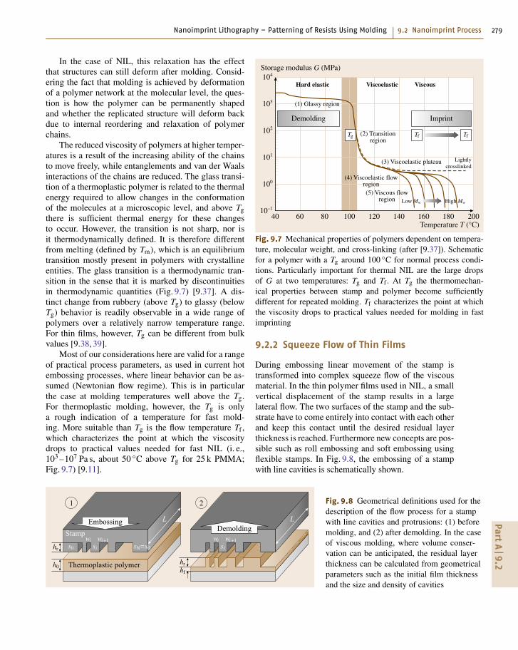
In the case of NIL, this relaxation has the effectthat structures can still deform after molding. Consid-ering the fact that molding is achieved by deformationof a polymer network at the molecular level, the ques-tion is how the polymer can be permanently shapedand whether the replicated structure will deform backdue to internal reordering and relaxation of polymerchains.
The reduced viscosity of polymers at higher temper-atures is a result of the increasing ability of the chainsto move freely, while entanglements and van der Waalsinteractions of the chains are reduced. The glass transi-tion of a thermoplastic polymer is related to the thermalenergy required to allow changes in the conformationof the molecules at a microscopic level, and above Tgthere is sufficient thermal energy for these changesto occur. However, the transition is not sharp, nor isit thermodynamically defined. It is therefore differentfrom melting (defined by Tm), which is an equilibriumtransition mostly present in polymers with crystallineentities. The glass transition is a thermodynamic tran-sition in the sense that it is marked by discontinuitiesin thermodynamic quantities (Fig. 9.7) [9.37]. A dis-tinct change from rubbery (above Tg) to glassy (belowTg) behavior is readily observable in a wide range ofpolymers over a relatively narrow temperature range.For thin films, however, Tg can be different from bulkvalues [9.38, 39].
Most of our considerations here are valid for a rangeof practical process parameters, as used in current hotembossing processes, where linear behavior can be as-sumed (Newtonian flow regime). This is in particularthe case at molding temperatures well above the Tg.For thermoplastic molding, however, the Tg is onlya rough indication of a temperature for fast mold-ing. More suitable than Tg is the flow temperature Tf ,which characterizes the point at which the viscositydrops to practical values needed for fast NIL (i. e.,103 –107 Pa s, about 50 ◦C above Tg for 25 k PMMA;Fig. 9.7) [9.11].
LEmbossingStamp
Thermoplastic polymerHard substrate
hr
hr
hfh0
s0 siwi wi+1
sN=s0
DemoldingL
1 2
wi wi+1si
Fig. 9.8 Geometrical definitions used for thedescription of the flow process for a stampwith line cavities and protrusions: (1) beforemolding, and (2) after demolding. In the caseof viscous molding, where volume conser-vation can be anticipated, the residual layerthickness can be calculated from geometricalparameters such as the initial film thicknessand the size and density of cavities
40 60 80 100 120 140 160
Low Mw High Mw
Lightlycrosslinked
180
(1) Glassy region
(2) Transitionregion
(3) Viscoelastic plateau
(4) Viscoelastic flowregion(5) Viscous flow
region
Demolding
Hard elastic Viscoelastic Viscous
Tg Tf Tf
Imprint
200
Storage modulus G (MPa)
Temperature T (°C)
104
103
102
101
100
10–1
Fig. 9.7 Mechanical properties of polymers dependent on tempera-ture, molecular weight, and cross-linking (after [9.37]). Schematicfor a polymer with a Tg around 100 ◦C for normal process condi-tions. Particularly important for thermal NIL are the large dropsof G at two temperatures: Tg and Tf . At Tg the thermomechan-ical properties between stamp and polymer become sufficientlydifferent for repeated molding. Tf characterizes the point at whichthe viscosity drops to practical values needed for molding in fastimprinting
9.2.2 Squeeze Flow of Thin Films
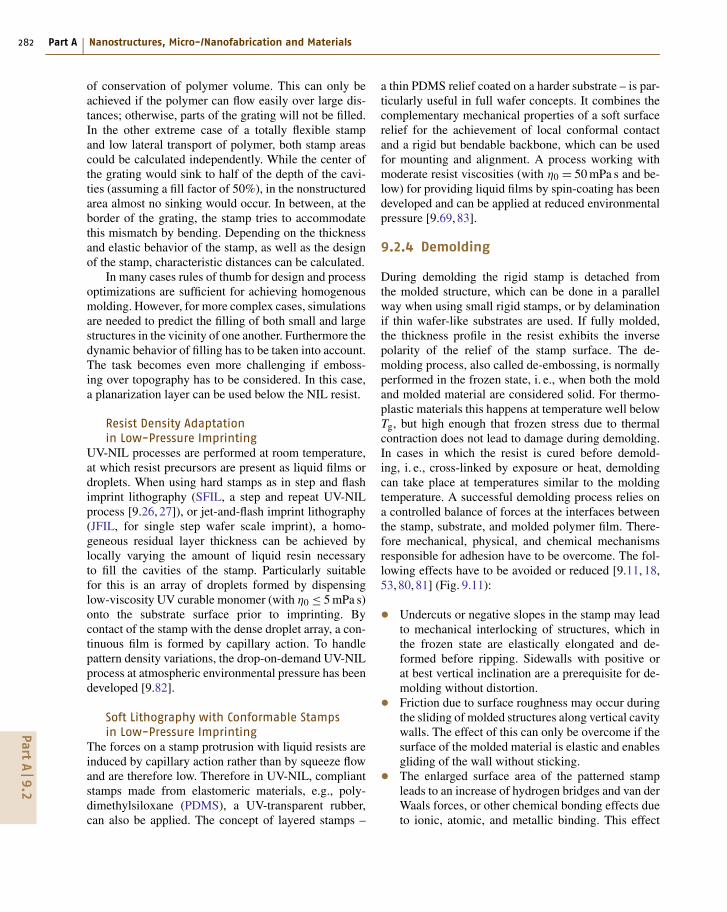
During embossing linear movement of the stamp istransformed into complex squeeze flow of the viscousmaterial. In the thin polymer films used in NIL, a smallvertical displacement of the stamp results in a largelateral flow. The two surfaces of the stamp and the sub-strate have to come entirely into contact with each otherand keep this contact until the desired residual layerthickness is reached. Furthermore new concepts are pos-sible such as roll embossing and soft embossing usingflexible stamps. In Fig. 9.8, the embossing of a stampwith line cavities is schematically shown.
PartA
9.2

280 Part A Nanostructures, Micro-/Nanofabrication and Materials
Before embossing, the polymer film has an initialthickness h0 and the depth of the microrelief is hr.For a fully inserted stamp, the film thickness underthe single stamp protrusions (elevated structures) withwidth si is hf . We can calculate this specific residuallayer height hf by applying the continuity equation withthe assumption that the polymer melt is incompressible(conservation of polymer volume). It can be directly de-duced from the fill factor ν, i. e., the ratio of the areacovered by cavities to the total stamp area
hf = h0 −νhr with ν =∑
iwi∑
i (si +wi ). (9.1)
This formula only applies for rigid stamps with constantfill factor.
A simple model for the squeezed polymer flow un-derneath the stamp protrusion is obtained by treatingthe polymer as an incompressible liquid of constantviscosity, and solving the Navier–Stokes equation withnonslip boundary conditions at the stamp and substratesurfaces. According to this model, given for line-shapedstamp protrusions and cavities in [9.13, 18, 40, 41], wefind the following expression, known as the Stefanequation [9.42], for the film thickness h(t) underneaththe stamp protrusion when a constant imprint force F isapplied to the single stamp protrusion
1
h2(t)= 1
h20
+ 2F
η0 Ls3t . (9.2)
Inserting the final thickness hf ≡ h(tf ) into (9.2) givesthe embossing time
tf = η0Ls3
2F
(1
h2f
− 1
h20
)
. (9.3)
For many practical cases, where a constant pressure un-der each stamp protrusion p = F/(sL) is assumed, thisformula gives
tf = η0s2
2p
(1
h2f
− 1
h20
)
. (9.4)
As a direct consequence of the Stefan equation it canbe seen that, at identical pressure, small (narrow) stampprotrusions will sink faster than large (wide) ones. Thestamp geometry can therefore be optimized by reducingthe dimensions of the protrusions. While stamps withnanopillar arrays, as shown in Fig. 9.2, would allow fastembossing of some microseconds, using standard NILprocess parameters, already protrusions of some hun-dreds of microns would increase embossing times to
t0
hf
Height
h0
Timetf
50%
95%
100%
Fig. 9.9 Schematic (right) of the squeeze flow of a com-pressed polymer film into one cavity. Once the cavity isfilled the stamp continues to sink but at a much slower rate(left), as a direct consequence of the Stefan equation
some hours. The strong dependence of the embossingtime on the pressing area has the consequence that, fora fully inserted stamp relief (full contact over the to-tal stamp area), the flow practically stops (as shownschematically in Fig. 9.9). For this case, s becomes largeand flow continues only towards the stamp borders. Itis also evident that there is only a weak influence ofthe embossing force (tf ∝ 1/F). At first sight there isa similar weak influence for η0. However, the viscositycan be changed significantly by varying the tempera-ture. For practical use, it is quite important that tradeoffsare possible between structure height, resist thickness,pressure, and temperature. For example, within certainlimits, a low imprint pressure can be compensated bya longer time or a higher temperature.
For completeness we now give the expressionsimilar to (9.3), but derived for a cylindrical stamp pro-trusion with radius R, i. e., with a stamp protrusion areaof π R2
1
h2(t)= 1
h20
+ 4F
3πη0 R4t . (9.5)
We present an example illustrating the conse-quences of these equations. In Fig. 9.10a we showa stamp which contains an array of small structures inthe center while the large single stamp protrusions sur-rounding the array dominate the sinking velocity (largesi ). The array in Fig. 9.10a is equivalent to the micro-cavity in Fig. 9.10b, which has the same volume as thetotal volume of the cavity array. This simplification canbe used for the calculation of embossing times. The fillfactor should be kept constant, both locally (at lengthscales corresponding to the cavity dimensions) and alsoacross the wafer, i. e., for large stamp protrusions, to en-sure better flow of the polymer and shorter embossing
PartA
9.2

Nanoimprint Lithography – Patterning of Resists Using Molding 9.2 Nanoimprint Process 281
Sink structures
Nanostructures
Microcavity
a)
b)
c)
Fig. 9.10a–c Comparison of the squeeze flow for a nano-and microcavities (schematics). In the case of an arrayof nanocavities and a single microcavity, surrounded bylarge unstructured stamp areas, the polymer has to flowover large distances, thus leading to long molding time.By the introduction of additional sink microstructures, ora denser arrangement of cavities, faster and more homoge-neous molding can be achieved (left: top view; right: sideview)
times. For this purpose, additional protrusions or cavi-ties can be placed in intermediate areas not needed forthe device function (Fig. 9.10c), or structures can be re-peated several times. We would also like to draw thereader’s attention to the fact that the different sinkingrates of protrusions of different sizes means that thestamp, which is normally backed by an elastic siliconemattress, can bend locally. This will result in a residuallayer height that is not uniform over the entire emboss-ing area.
The implications of squeeze flow are discussedin more detail in [9.43–46], including rheologicalissues [9.47–59], bending of stamps in large-area im-printing [9.44, 60–69], and the influence of vacuumand self-assembly [9.70–79]. More information canalso be found in Sect. 9.2.6 about pattern transfer andSect. 9.3.1 for NIL materials.
9.2.3 Residual Layer ThicknessHomogeneity
The main difference between NIL and lithographybased on exposure and development is that a residuallayer below the stamp protrusions is left after demold-ing. As seen before, this is a result of the moldingprocess slowing down due to the squeeze flow. Formany applications, when pattern transfer has to beachieved after the embossing, it is important to deter-mine the final residual thickness hf of this polymerlayer (Fig. 9.8) before the next process step. Further-
more it is important to know the thickness variationover the embossed area; otherwise, parts of the struc-ture will be lost during pattern transfer. As will beshown in the following, bending of stamps has to betaken into account, as well as effects such as air inclu-sions, dewetting, and self-assembly of resist [9.18, 72].In most cases a homogeneous residual layer can beachieved by optimizing the pattern design, but also byusing adapted processes which create thin residual lay-ers independent of the design. In contrast to this, patterntransfer processes which are insensitive to thicknessvariations have to be used, e.g., by using a resist withhigh etch resistance or an intermediate layer as a hardmask. The following examples demonstrate how softand hard elements for equilibration are used to achievehomogeneous molding.
Bending of Stamps in High-PressureImprinting
In NIL, the stamp is often considered as a hard toolwhich is inflexible over millimeter distances. However,this is only true for special cases, e.g., when densityand size of stamp protrusions are homogeneous overthe whole stamp surface. Furthermore it is strongly de-pendent on the pressure used, and therefore only playsa significant role in current hot embossing processes.Local bending of some nanometers occurring due tosmall local variations of the stamp geometry has to beconsidered as the general case during hot embossing ofthin films [9.18,53,80,81]. Both the global movement ofup to a few hundred nanometers, and the compensationof local height variations of a few tens of nanome-ters, are easy to implement with a compliance-typemechanism. In presses with a stiff mechanism basedon hydraulic, air, and screw-driven hard stampers, thebuild-up of the whole stack includes the use of an elas-tic compliance layer (e.g., flexible graphite, rubber orteflon), which is needed for surface equilibration dueto the lack of flatness of common substrates. Other con-cepts use an air-pressurized membrane as a soft cushion,which equilibrates local pressure variations during thesinking of the stamp in a more controlled way.
For a typical case where the grating is surrounded bya large unstructured area, stamp bending results in an in-homogeneous residual layer at the border of the grating.Figure 9.10a shows such a case, in which a grating area,typically of some square millimeters, is surrounded bya large nonstructured area. In the ideal case of a totallyrigid stamp, the final thickness would be determined bythe fill factor of the grating averaged over the wholestamp area, which could be calculated by the simple rule
PartA
9.2
282 Part A Nanostructures, Micro-/Nanofabrication and Materials
of conservation of polymer volume. This can only beachieved if the polymer can flow easily over large dis-tances; otherwise, parts of the grating will not be filled.In the other extreme case of a totally flexible stampand low lateral transport of polymer, both stamp areascould be calculated independently. While the center ofthe grating would sink to half of the depth of the cavi-ties (assuming a fill factor of 50%), in the nonstructuredarea almost no sinking would occur. In between, at theborder of the grating, the stamp tries to accommodatethis mismatch by bending. Depending on the thicknessand elastic behavior of the stamp, as well as the designof the stamp, characteristic distances can be calculated.
In many cases rules of thumb for design and processoptimizations are sufficient for achieving homogenousmolding. However, for more complex cases, simulationsare needed to predict the filling of both small and largestructures in the vicinity of one another. Furthermore thedynamic behavior of filling has to be taken into account.The task becomes even more challenging if emboss-ing over topography has to be considered. In this case,a planarization layer can be used below the NIL resist.
Resist Density Adaptationin Low-Pressure Imprinting
UV-NIL processes are performed at room temperature,at which resist precursors are present as liquid films ordroplets. When using hard stamps as in step and flashimprint lithography (SFIL, a step and repeat UV-NILprocess [9.26, 27]), or jet-and-flash imprint lithography(JFIL, for single step wafer scale imprint), a homo-geneous residual layer thickness can be achieved bylocally varying the amount of liquid resin necessaryto fill the cavities of the stamp. Particularly suitablefor this is an array of droplets formed by dispensinglow-viscosity UV curable monomer (with η0 ≤ 5 mPa s)onto the substrate surface prior to imprinting. Bycontact of the stamp with the dense droplet array, a con-tinuous film is formed by capillary action. To handlepattern density variations, the drop-on-demand UV-NILprocess at atmospheric environmental pressure has beendeveloped [9.82].
Soft Lithography with Conformable Stampsin Low-Pressure Imprinting
The forces on a stamp protrusion with liquid resists areinduced by capillary action rather than by squeeze flowand are therefore low. Therefore in UV-NIL, compliantstamps made from elastomeric materials, e.g., poly-dimethylsiloxane (PDMS), a UV-transparent rubber,can also be applied. The concept of layered stamps –
a thin PDMS relief coated on a harder substrate – is par-ticularly useful in full wafer concepts. It combines thecomplementary mechanical properties of a soft surfacerelief for the achievement of local conformal contactand a rigid but bendable backbone, which can be usedfor mounting and alignment. A process working withmoderate resist viscosities (with η0 = 50 mPa s and be-low) for providing liquid films by spin-coating has beendeveloped and can be applied at reduced environmentalpressure [9.69, 83].
9.2.4 Demolding
During demolding the rigid stamp is detached fromthe molded structure, which can be done in a parallelway when using small rigid stamps, or by delaminationif thin wafer-like substrates are used. If fully molded,the thickness profile in the resist exhibits the inversepolarity of the relief of the stamp surface. The de-molding process, also called de-embossing, is normallyperformed in the frozen state, i. e., when both the moldand molded material are considered solid. For thermo-plastic materials this happens at temperature well belowTg, but high enough that frozen stress due to thermalcontraction does not lead to damage during demolding.In cases in which the resist is cured before demold-ing, i. e., cross-linked by exposure or heat, demoldingcan take place at temperatures similar to the moldingtemperature. A successful demolding process relies ona controlled balance of forces at the interfaces betweenthe stamp, substrate, and molded polymer film. There-fore mechanical, physical, and chemical mechanismsresponsible for adhesion have to be overcome. The fol-lowing effects have to be avoided or reduced [9.11, 18,53, 80, 81] (Fig. 9.11):
• Undercuts or negative slopes in the stamp may leadto mechanical interlocking of structures, which inthe frozen state are elastically elongated and de-formed before ripping. Sidewalls with positive orat best vertical inclination are a prerequisite for de-molding without distortion.• Friction due to surface roughness may occur duringthe sliding of molded structures along vertical cavitywalls. The effect of this can only be overcome if thesurface of the molded material is elastic and enablesgliding of the wall without sticking.• The enlarged surface area of the patterned stampleads to an increase of hydrogen bridges and van derWaals forces, or other chemical bonding effects dueto ionic, atomic, and metallic binding. This effect
PartA
9.2

Nanoimprint Lithography – Patterning of Resists Using Molding 9.2 Nanoimprint Process 283
can only be overcome if the stamp surface can beprovided with sufficient antiadhesive properties.
The most critical point is that demolding forces largelydepend on the geometry of the mold, and the overall de-sign of a stamp structure has to be taken into account.Therefore structures with high aspect ratio may be moreprone to ripping, and if many neighboring structures ex-ert high forces on the underlying substrate, whole areasof resist may be detached from the substrate surface.Antiadhesion layers on the mold can reduce frictionforces, but have to be thin and durable. In thermal NILthe expansion coefficient of the substrate αsubstrate andof the stamp αstamp should be similar, to avoid distor-tion due to mechanical stress induced by cooling. In thecase of very thin polymer layers, the lateral thermal ex-pansion of the resist is determined by the substrate. Forstructures with higher aspect ratio the demolding tem-perature Tdemold should be well below Tg, to enable thedemolding of a hardened resist without distortion, butas near as possible to Tg, because the stress induced bythermal shrinkage should not exceed a maximum valuein critical areas where structures tend to break.
9.2.5 Curing of Resists
Curing by UV exposure, by thermal treatment or bychemical initiation is a way to cross-link polymers andmake them durable for demolding [9.24, 25, 27, 82–96]. A high reaction speed, as caused by a high ex-posure dose, high initiator content or curing at hightemperatures, leads to fast but weak cross-linking,whereas a slow reaction leads to highly polymerized,tougher materials because the slow polymerization en-ables a more complete process. As shown in Sect. 9.1.2,various process strategies have been developed. In mostof them the curing step is independent of the moldingstep, and can be initiated by light or a specific tempera-ture after molding is complete. Because curing involvesa change in the physical conformation of the polymer,it always goes along with volumetric shrinkage of thepolymer; e.g., acrylate polymerization is known to beaccompanied by volumetric shrinkage that is the re-sult of chemical bond formation. Consequently, the size,shape, and placement of the replicated features maybe affected. In the following the main processes whichinvolve curing are presented in more detail:
• In the UV-NIL process, as used in SFIL [9.26, 27],the resist is cured after molding but before de-molding of the stamp. The process relies on thephotopolymerization of a low-viscosity, acrylate-
a)
V
V V
c)b)
d) e) f )
Fig. 9.11a–f Demolding issues: (a) generation of vacuum voids (V),(b) elongation and ripping of single structures, (c) ripping of resistfrom substrate, (d) penetration of air into voids (inclined sidewalls),(e) shrinkage and generation of rims, and (f) relaxation of frozen-instrain (after [9.11])
based solution. Shrinkage was found to be lessthan 10% of total volume in most cases. Thecurrent liquid is a multicomponent solution. Thesilylated monomer provides etch resistance in theO2 transfer etch, and is therefore called the etchbarrier. Cross-linker monomers provide thermal sta-bility to the cured etch barrier and also improveits cohesive strength. Organic monomers serve asmass-persistent components and lower the viscosityof the etch barrier formulation. The photoinitiatorsdissociate to form radicals upon UV irradiation, andthese radicals initiate polymerization.• If a solid curable resist exhibits thermoplastic be-havior, it can be molded at an elevated temperatureand then cross-linked, either before or after demold-ing. The advantage of the process is that low-Mwresists with low Tg can be provided, which can beprocessed at moderate temperatures. However, be-fore pattern transfer, hardening is often necessary.They can also be used for mix-and-match with PLor for polymeric stamp copies.• Thermoset resists can be cross-linked by heat. Hereit is of advantage that the temperature for mold-ing is lower than the curing temperature. Then thestructure is first molded and then heated to its cross-linking temperature to induce cross-linking, beforethe stamp is demolded from the hardened surfacerelief.
PartA
9.2

284 Part A Nanostructures, Micro-/Nanofabrication and Materials
More information about curing and multilayer resistscan be found in Sect. 9.3.
9.2.6 Pattern Transfer
In many cases the lithographic process is only completewhen the resist pattern is transferred to another ma-terial. This process, in which the resist is transformedinto a patterned masking layer, allows the substrate tobe attacked by plasma, etching solutions, electroplat-ing, deposition of materials, and other substrate-alteringprocesses. A unique advantage of molding instead ofexposure is that complex stamp profiles, such as staircases, V-grooves, and pyramids, both convex and con-cave, can be replicated. They can be used for thegeneration of 3-D structures such as for T-gate transis-tors or contact holes, or serve for stepwise etching ofunderlying layers with variation of the opening width.As long as undercuts and 3-D patterning are not nec-essary, in most cases this pattern transfer is thereforesimilar to in EBL. However, in this section we em-phasize methods where NIL has some specific processadvantages over conventional lithographic methods, orwhere the use of NIL implies some major changes in thefabrication process or properties of the devices:
• In NIL, etching is used for both the removal of theresidual layer and the pattern transfer of the resistpattern to the underlying substrate [9.7, 97–106].In the first case the polymer layer has to be ho-mogeneously thinned down until openings to the
Spincoating ofthermoplast onhard substrate
Compression molding
Stampwith nanorelief
Hot embossingand demolding
Metal lanes(period 1µm)PMMA: 50 nmNickel: 45 nm
Pattern transfer
Seed layerwindow opening
Electroforming
Removing ofresist and seedlayer
500% overplatedPMMA: 45nmNickel: 270nm
Fig. 9.12 NIL and electroforming:Electrode structures have been fabri-cated in Ni by using a plating baseof Cr and Ge. After plating on top ofthe Ge, both layers of the plating basecan be etched using RIE (Cr: chlorinechemistry; Ge: SF6). Even with 500%overplating, the thick electrodes stayseparated (after [9.97])
underlying substrate are generated. This is alsocalled a window-opening or breakthrough etch. Inthe second case the thickness contrast of the remain-ing polymer is used to mask the substrate against theetching medium. Both processes have to be highlyanisotropic, i. e., during the transfer step the lateralsize of the structure has to be preserved, includingthe slope of the original pattern. Apart from open-ing windows using reactive-ion etching (RIE), otherpattern transfer strategies have been found whichcircumvent the residual layer problem.• Lift-off is a patterning technique adding thin lay-ers of a solid material (e.g., metal) locally to thewindow openings in the resist [9.107–114]. Un-dercuts, as can be generated in PL and EBL, area prerequisite for good lift-off. However, in NIL,where sidewalls are at best vertical, a high thicknesscontrast (aspect ratio) of the structures is needed.Lift-off resists are a means to generate defined un-dercuts using a bilayer resist system, by selectivelydissolving a sacrificial bottom layer through thestructured openings of a top layer.• Electroforming and electroplating, like lift-off, areprocesses that add material to the areas not cov-ered by the resist [9.97, 115, 116]. Electroformingprovides a good alternative to the lift-off processbecause metal structures can be generated withconsiderable height and good surface quality. Ifa conductive seed layer is deposited below the resist,during electroplating the metal layer starts to growfrom within the window regions and conforms to the
PartA
9.2
Nanoimprint Lithography – Patterning of Resists Using Molding 9.2 Nanoimprint Process 285
outlines of the cavities in the resist. Depending onthe extent of electroplating, the structure height canbe either preserved or increased.
Some of the examples presented here for pattern trans-fer already give insight into simple demonstrators, par-ticularly when the application is based on a simple pat-tern transfer or NIL is used as the first patterning step ofa nonstructured surface. Examples of applications are:
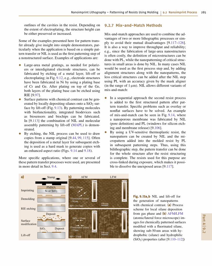
• Large-area metal gratings, as needed for polariz-ers or interdigitated electrode structures, can befabricated by etching of a metal layer, lift-off orelectroplating; in Fig. 9.12, e.g., electrode structureshave been fabricated in Ni by using a plating baseof Cr and Ge. After plating on top of the Ge,both layers of the plating base can be etched usingRIE [9.97].• Surface patterns with chemical contrast can be gen-erated by locally depositing silanes onto a SiO2 sur-face by lift-off (Fig. 9.13). By patterning moleculeswith biofunctionality, integrated biodevices suchas biosensors and biochips can be fabricated.In [9.113] the combination of NIL and molecularassembly patterning by lift-off (MAPL) is demon-strated.• By etching, the NIL process can be used to drawcopies from a stamp original [9.44, 99, 115]. Oftenthe deposition of a metal layer for subsequent etch-ing is used as a hard mask to generate copies withan enhanced aspect ratio (Figs. 9.14 and 9.18).
More specific applications, where one or several ofthese pattern transfer processes were used, are presentedin more detail in Sect. 9.4.
AFM
Surfacemodification
SiO2 ≈20nm
Fluorinated silane≈50nm
HP= 35.5nm
SiO2 ≈15nm
LFM
Deposit
DepositSiO2
Si or SiO2
PMMA
100 nm
0nm
3nm
0V
0.15V
0nm
3nm
0V
0.15V
100 nm
Fluorinated silane≈35nm
HP = 25nm
Stamp
Lift-off
RIE etching
Demolding
Imprinting
a) b)
Fig. 9.13a,b NIL and lift-off forthe generation of nanopatternswith chemical contrast. (a) Processscheme for local silane depositionfrom gas phase and (b) AFM/LFM(atomic/lateral force microscope) im-ages for chemically patterned surfacesmodified with a fluorinated silane,showing sub-50 nm areas with hy-drophobic (silane) and hydrophilic(SiO2) properties (after [9.110–112])
9.2.7 Mix-and-Match Methods
Mix-and-match approaches are used to combine the ad-vantages of two or more lithographic processes or sim-ply to avoid their mutual disadvantages [9.117–126].It is also a way to improve throughput and reliability;e.g., since the fabrication of large-area nanostructuresis often costly, the definition of microstructures can bedone with PL, while the nanopatterning of critical struc-tures in small areas is done by NIL. In many cases NILwould be used as the first process step and, by addingalignment structures along with the nanopatterns, theless critical structures can be added after the NIL stepusing PL with an accuracy given by the mask aligner(in the range of 1 μm). NIL allows different variants ofmix-and-match:
• In a sequential approach the second resist processis added to the first structured pattern after pat-tern transfer. Specific problems such as overlay ornonflat surfaces have to be solved. An exampleof mix-and-match can be seen in Fig. 9.14, wherea nanoporous membrane was fabricated by NIL(pore definition) and PL (windows for silicon etch-ing and membrane release) [9.106].• By using a UV-sensitive thermoplastic resist, thenanopattern can be created by NIL and the mi-cropattern added into the molded resist by PLin subsequent patterning steps. Thus, using thisbilithographic step, the pattern transfer can be donefor the whole structure after the resist structuringis complete. The resists used for this purpose arecross-linked during exposure, which makes it possi-ble to dissolve the unexposed areas [9.117].
PartA
9.2

286 Part A Nanostructures, Micro-/Nanofabrication and Materials
b)PMMACrSi3N4
Si3N4
Si
c)
a)
1µm
5µm
NIL stamp
Fig. 9.14a–c Mix- and match of NIL and silicon micromachining:(a) process scheme for the fabrication of nanopores in a Si3N4
membrane. SEM images (b) of the NIL stamps (pillars) and (c) thecorresponding nanopores (after [9.106])
• A specific mix-and-match approach is possible ifUV exposure is done before the stamp is detachedfrom the molded resist. This is possible when partsof the stamp are transparent (e.g., the recessedareas), while the protrusions are coated with anopaque layer (e.g., a metal masking layer such asthat used for etching the stamp structures) [9.119].This makes it possible to cross-link the thick resistareas while the residual layer can be dissolved.
9.2.8 Multilayer and Multilevel Systems
Multilayer resist systems are used if the etching selec-tivity of a masking layer has to be enhanced, e.g., for
Release layer
Template
a)Etch barriersolution
Transfer layerb) c) d) e)
Curred etch barrierResidual layer
UV
Fig. 9.15a–e Process scheme of UV imprinting and pattern transfer, using a double layer (also called direct SFIL). Themolded top layer, also called the etch barrier, is coated on a transfer layer, which serves as a planarization layer. It hasalso antireflective properties for the UV exposure through the stamp. (a) dispensing of viscous resist droplet, (b) imprint,(c) UV-exposure and curing, (d) demolding of hardened resist, (e) residual layer etch and transfer into bottom layer(breakthrough etch/window opening)
the fabrication of high-aspect-ratio structures, undercutshave to be generated, e.g., for lift-off, or a planarizationlayer has to be employed for printing over topogra-phy [9.127–134].
The most important application of double resistsis for low-pressure processes such as UV molding(Fig. 9.15). For prestructured substrates with topogra-phy, a planarization layer is needed, because the lowpressure of below 1 bar is often not sufficient to achieveconformal contact of the transparent mask with the non-flat substrate surface; otherwise parts of the resist stayunmolded. Multilayer resist approaches with a thickpolymer planarization layer on top of the substrate re-quire complex processes with multiple steps but alsoentail deep etching steps to etch through the thick pla-narization layer, which often degrades the resolutionand fidelity of the pattern. Bilayer resists are also usedfor better lift-off. For this purpose lift-off resists (LOR)have been developed [9.135]; they are coated below thetop layer and can be selectively removed by wet devel-opment through the patterned top layer. The developersused are adapted to generate undercuts in LOR layersof some tens of nanometers up to some microns. Theneven a curable resist which is cross-linked (equivalentto a negative resist) can be used as a top layer, whilethe sacrificial bottom layer makes it possible to releasethe top layer as well as the metal layer used for lift-off.
Often top layers with high etching resistance,e.g., silicon-containing resists (similar to hardening bysilanization), are chosen for UV-NIL. After moldingthe top layer, the pattern is transferred to the under-lying planarization (transfer) layer. The top layer canbe kept thin, while the etching depth can be furtherincreased by choosing a thick bottom layer. Normallythe tone of a stamp pattern is inverted when etching
PartA
9.2
Nanoimprint Lithography – Patterning of Resists Using Molding 9.2 Nanoimprint Process 287
Bottom layer(with wires)
Breakthroughetch
IBM powerPX750micro-processor(cross sectionof contactlayer)
Stamp(transparent)
Resistbottom layer(with seal)
Molding andexposure ofresist throughstamp
Seed layerdeposition
Metallization(copperelectroplating)
Metalthinning(CMPprocess)
DemoldingMetal 6
Metal 5M5 VIA
Metal 2
M2 Seal
Substrate
ILD 1-1
M4 VIA
0)
a)
b)
1)
2)
3)
4)
5)
6)
7)
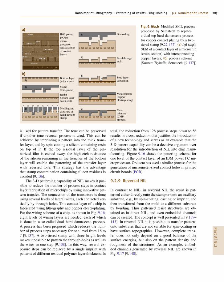
Fig. 9.16a,b Modified SFIL processproposed by Sematech to replacea dual top hard damascene processfor copper contact plating by a two-tiered stamp [9.27, 137]. (a) left (top):SEM of a contact layer of a microchip(cross section) with interconnectingcopper layers, (b) process scheme(Source: Trybulla, Sematech, [9.137])
is used for pattern transfer. The tone can be preservedif another tone reversal process is used. This can beachieved by imprinting a pattern into the thick trans-fer layer, and by spin-coating a silicon-containing resinon top of it. If the top residual layer of the pla-narized film is etched away, the high etch resistanceof the silicon remaining in the trenches of the bottomlayer will enable the patterning of the transfer layerwith reversed tone. This strategy has the advantagethat stamp contamination containing silicon residues isavoided [9.136].
The 3-D patterning capability of NIL makes it pos-sible to reduce the number of process steps in contactlayer fabrication of microchips by using innovative pat-tern transfer. The connection of the transistors is doneusing several levels of lateral wires, each contacted ver-tically by through-holes. This contact layer of a chip isfabricated using lithography and copper electroplating.For the wiring scheme of a chip, as shown in Fig. 9.16,eight levels of wiring layers are needed, each of whichis done in a so-called dual hard damascene process.A process has been proposed which reduces the num-ber of process steps necessary for one level from 16 to7 [9.137]. A two-tiered stamp with three height levelsmakes it possible to pattern the through-holes as well asthe wires in one step [9.138]. In this way, several ex-posure steps can be replaced by a single imprint withpatterns of different residual polymer layer thickness. In
total, the reduction from 128 process steps down to 56results in a cost reduction that justifies the introductionof a new technology and serves as an example that the3-D pattern capability can be a decisive argument overresolution for the introduction of NIL into chip manu-facturing. Figure 9.16 shows the pattering scheme forone level of the contact layer of an IBM power PC mi-croprocessor. Obducat has used a similar process for thegeneration of micrometer-sized contact holes in printedcircuit boards (PCB).
9.2.9 Reversal NIL
In contrast to NIL, in reversal NIL the resist is pat-terned either directly onto the stamp or onto an auxiliarysubstrate, e.g., by spin-coating, casting or imprint, andthen transferred from the mold to a different substrateby bonding. Thus patterned resist structures are ob-tained as in direct NIL, and even embedded channelscan be created. The concept is well presented in [9.139–143]. In reversal NIL it is possible to transfer patternsonto substrates that are not suitable for spin-coating orhave surface topographies. However, complete trans-fer does not only depend on a good balance of thesurface energies, but also on the pattern density androughness of the structures. As an example, embed-ded channels generated by reversal NIL are shown inFig. 9.17 [9.140].
PartA
9.2

288 Part A Nanostructures, Micro-/Nanofabrication and Materials
9.3 Tools and Materials for Nanoimprinting
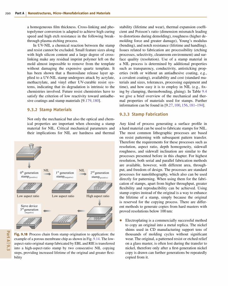
Mechanical nanofabrication techniques based on mold-ing need tools and materials with matched mechanicalproperties. The mold has to be made from a materialwhich is sufficiently hard to sustain at least one pro-cessing cycle. From the viewpoint of mass fabrication,a mold is considered as a tool which survives the mold-ing process unaltered and uncontaminated, and thus canbe reused many times after each molding step. In thisway many identical replicas can be drawn (copied) fromone mold. Due to the conformal molding, the surfaceof these copies is the negative structure of the origi-nal (inverted polarity). Therefore a true replica of themold is generated, when a negative is again molded intoa positive structure. Here, we use the terms replica andcopy in the more general sense that also negatives areconsidered as true copies of an original.
As the terms imprinting, embossing, molding, andreplication are often used for the same process, differ-ent names for the replication tools exist depending ontheir origins: mold or mold insert for those coming frompolymer processing; master or stamp (stamper) from
Table 9.3 Properties of thermoplastic polymers for thermal NIL
Material(other names)
Solvent Glass transitiontemperature Tgand imprinttemperatureTimprint (◦C)
Viscosityat typicalimprinttemperature(Pa s) (Fig. 9.5)
Comments
Poly(methylmethacrylate) (PMMA)[9.135, 144–150]
Chlorobenzene,safe solvents
100 (at 160–190) 3 × 10⁴
(25 k at 180 ◦C)The classic NIL resist,refractive index n = 1.49 [9.6, 18]
Polystyrene (PS)[9.145]
Toluene 104 (150–170)[9.21]
1.8 × 10³
(58 k at 170 ◦C)Integrated optics, biology, n = 1.59 [9.147]
Polycarbonate (PC)[9.148, 149]
Cyclohexanone[9.23, 41, 150],1,1,2,2-tetra-chloroethane
148 (160–190) Integrated optics, n = 1.59high etching resistance [9.147]
mr-I T85 [9.144] Toluene[9.151]
85 (140–170)[9.152]
2 × 10⁴
(at 170 ◦C)[9.151]
Chemically resistant, low water absorption,highly transparent, n = 1.497 [9.153–155]
mr-NIL 6000 [9.144] Safe solvent 40 (100–110) 2 × 10³
(at 100 ◦C)UV-curable, low-Tg NIL resist for mix-and-match,multilevel patterning [9.156, 157]
mr-I 7000 [9.144] and E Safe solvent 60 (125–150) 3 × 10³ (E gradeat 140 ◦C)
Low Tg NIL resist, n = 1.415
mr-I 8000 [9.144] and E Safe solvent 115 (170–190) 7 × 10⁴ (E gradeat 180 ◦C)
n = 1.415, NIL resist with thermal propertiessimilar to PMMA, but higher etch resistance
mr-I 9000 [9.144] and E Safe solvent 65 (140–160) n = 1.417, thermocurable NIL resist [9.90]
NEB22 [9.158] PGMEA[9.159]
80 (95–130)[9.160]
Negative EBL resist based on poly(hydroxystyren),high etch resistance in fluoro- and chloro-basedplasmas [9.150], low Mw (3k)
CD fabrication; and template, mask, and die from thelithography community.
In this section we will have a closer look at conceptsfor tools, machines, and processes used for NIL. Wewill start with a discussion of resist materials for NIL,and then proceed with materials used for stamps. Wedescribe fabrication methods, both for original stampsand for stamp copies, and the use and application ofantiadhesive coatings. We will then present concepts forNIL machines, and how a homogeneous pressure dis-tribution is achieved for nanoreplication. For thermalimprinting as well as UV imprinting single-step wafer-scale processing and step-and-repeat approaches havebeen developed. The aim is to make the reader famil-iar with concepts rather than presenting machines andmaterials sold on the market.
9.3.1 Resist Materials for Nanoimprinting
Resists used for NIL are either used as an intermediatemasking layer for the substrate or as a functional layer
PartA
9.3
Nanoimprint Lithography – Patterning of Resists Using Molding 9.3 Tools and Materials for Nanoimprinting 289
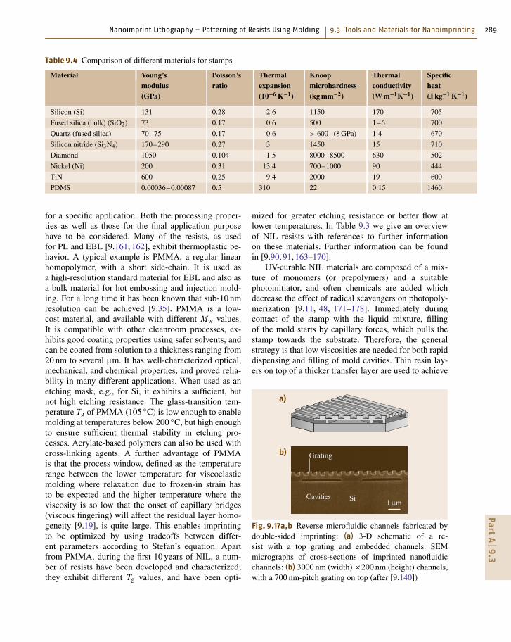
Table 9.4 Comparison of different materials for stamps
Material Young’s Poisson’s Thermal Knoop Thermal Specificmodulus ratio expansion microhardness conductivity heat(GPa) (10−6 K−1) (kg mm−2) (W m−1K−1) (J kg−1 K−1)
Silicon (Si) 131 0.28 2.6 1150 170 705
Fused silica (bulk) (SiO2) 73 0.17 0.6 500 1–6 700
Quartz (fused silica) 70–75 0.17 0.6 > 600 (8 GPa) 1.4 670
Silicon nitride (Si3N4) 170–290 0.27 3 1450 15 710
Diamond 1050 0.104 1.5 8000–8500 630 502
Nickel (Ni) 200 0.31 13.4 700–1000 90 444
TiN 600 0.25 9.4 2000 19 600
PDMS 0.00036–0.00087 0.5 310 22 0.15 1460
for a specific application. Both the processing proper-ties as well as those for the final application purposehave to be considered. Many of the resists, as usedfor PL and EBL [9.161, 162], exhibit thermoplastic be-havior. A typical example is PMMA, a regular linearhomopolymer, with a short side-chain. It is used asa high-resolution standard material for EBL and also asa bulk material for hot embossing and injection mold-ing. For a long time it has been known that sub-10 nmresolution can be achieved [9.35]. PMMA is a low-cost material, and available with different Mw values.It is compatible with other cleanroom processes, ex-hibits good coating properties using safer solvents, andcan be coated from solution to a thickness ranging from20 nm to several μm. It has well-characterized optical,mechanical, and chemical properties, and proved relia-bility in many different applications. When used as anetching mask, e.g., for Si, it exhibits a sufficient, butnot high etching resistance. The glass-transition tem-perature Tg of PMMA (105 ◦C) is low enough to enablemolding at temperatures below 200 ◦C, but high enoughto ensure sufficient thermal stability in etching pro-cesses. Acrylate-based polymers can also be used withcross-linking agents. A further advantage of PMMAis that the process window, defined as the temperaturerange between the lower temperature for viscoelasticmolding where relaxation due to frozen-in strain hasto be expected and the higher temperature where theviscosity is so low that the onset of capillary bridges(viscous fingering) will affect the residual layer homo-geneity [9.19], is quite large. This enables imprintingto be optimized by using tradeoffs between differ-ent parameters according to Stefan’s equation. Apartfrom PMMA, during the first 10 years of NIL, a num-ber of resists have been developed and characterized;they exhibit different Tg values, and have been opti-
mized for greater etching resistance or better flow atlower temperatures. In Table 9.3 we give an overviewof NIL resists with references to further informationon these materials. Further information can be foundin [9.90, 91, 163–170].
UV-curable NIL materials are composed of a mix-ture of monomers (or prepolymers) and a suitablephotoinitiator, and often chemicals are added whichdecrease the effect of radical scavengers on photopoly-merization [9.11, 48, 171–178]. Immediately duringcontact of the stamp with the liquid mixture, fillingof the mold starts by capillary forces, which pulls thestamp towards the substrate. Therefore, the generalstrategy is that low viscosities are needed for both rapiddispensing and filling of mold cavities. Thin resin lay-ers on top of a thicker transfer layer are used to achieve
Grating
a)
b)
Cavities Si 1µm
Fig. 9.17a,b Reverse microfluidic channels fabricated bydouble-sided imprinting: (a) 3-D schematic of a re-sist with a top grating and embedded channels. SEMmicrographs of cross-sections of imprinted nanofluidicchannels: (b) 3000 nm (width) × 200 nm (height) channels,with a 700 nm-pitch grating on top (after [9.140])
PartA
9.3
290 Part A Nanostructures, Micro-/Nanofabrication and Materials
a homogeneous film thickness. Cross-linking and pho-topolymer conversion is adapted to achieve high curingspeed and high etch resistance in the following break-through plasma etching process.
In UV-NIL a chemical reaction between the stampand resist cannot be excluded. Small feature sizes alongwith high silicon content and a large degree of cross-linking make any residual imprint polymer left on themold almost impossible to remove from the templatewithout damaging the expensive quartz template. Ithas been shown that a fluorosilane release layer ap-plied to a UV-NIL stamp undergoes attack by acrylate,methacrylate, and vinyl ether UV-curable resist sys-tems, indicating that its degradation is intrinsic to thechemistries involved. Future resist chemistries have tosatisfy the criterion of low reactivity toward antiadhe-sive coatings and stamp materials [9.179, 180].
9.3.2 Stamp Materials
Not only the mechanical but also the optical and chem-ical properties are important when choosing a stampmaterial for NIL. Critical mechanical parameters andtheir implications for NIL are hardness and thermal
0th generationstamp(positive)
Low aspect ratio
NIL
Low aspect ratio High aspect ratio
1st generationstamp(negative)
2nd generationstamp(positive)
NIL
Sieve device3rd generation
(negative)
Fig. 9.18 Process chain from stamp origination to application: theexample of a porous membrane chip as shown in Fig. 9.14. The low-aspect-ratio original stamp fabricated by EBL and RIE is transferredinto a high-aspect-ratio stamp by two consecutive NIL copyingsteps, providing increased lifetime of the original and greater flexi-bility
stability (lifetime and wear), thermal expansion coeffi-cient and Poisson’s ratio (dimension mismatch leadingto distortions during demolding), roughness (higher de-molding force and greater damage), Young’s modulus(bending), and notch resistance (lifetime and handling).Issues related to fabrication are processibility (etchingprocesses, selectivity, cleanroom environment) and sur-face quality (resolution). Use of a stamp material ina NIL process is determined by additional propertiessuch as transparency, conductivity, antisticking prop-erties (with or without an antiadhesive coating, e.g.,a covalent coating), availability and cost (standard ma-terials and sizes, tolerances, processing equipment andtime), and how easy it is to employ in NIL (e.g., fix-ing by clamping, thermobonding, gluing). In Table 9.4we give a brief overview of the mechanical and ther-mal properties of materials used for stamps. Furtherinformation can be found in [9.27, 100, 156, 181–194].
9.3.3 Stamp Fabrication
Any kind of process generating a surface profile ina hard material can be used to fabricate stamps for NIL.The most common lithographic processes are basedon resist patterning with subsequent pattern transfer.Therefore the requirements for these processes such asresolution, aspect ratio, depth homogeneity, sidewallroughness, and sidewall inclination are similar to theprocesses presented before in this chapter. For highestresolution, both serial and parallel fabrication methodsare available, however, with different area, through-put, and freedom of design. The processes are standardprocesses for nanolithography, which also can be useddirectly for patterning. When using them for the fabri-cation of stamps, apart from higher throughput, greaterflexibility and reproducibility can be achieved. Usingstamp copies instead of the original is a way to enhancethe lifetime of a stamp, simply because the originalis reserved for the copying process. There are differ-ent methods to generate copies from hard masters withproved resolutions below 100 nm:
• Electroplating is a commercially successful methodto copy an original into a metal replica. The nickelshims used in CD manufacturing support tens ofthousands of molding cycles without significantwear. The original, a patterned resist or etched reliefon a glass master, is often lost during the transfer tonickel, therefore only after a first-generation nickelcopy is drawn can further generations be repeatedlycopied from it.
PartA
9.3

Nanoimprint Lithography – Patterning of Resists Using Molding 9.3 Tools and Materials for Nanoimprinting 291
• Using the hard master with an etched surface reliefdirectly as a mold is a straightforward approach ifthe mechanical setup allows or favors the use of sil-icon (Si) or fused silica (SiO2). Stamp copies can befabricated using NIL and subsequent pattern trans-fer (Fig. 9.18). Molds made from silicon wafers arewell suited to use as stamps in NIL, and have evenshown their mass-fabrication capability in CD in-jection molding. For UV-NIL such as SFIL, moldswere successfully made using standard mask blanks(fused silica).• As a third solution a polymer or sol–gel layer withan imprinted surface relief can be directly used asa replication tool. This is possible if the thermo-mechanical replication process does not exert highforces on the relief structure. Resist hardened bylight, heat or by chemical initiation may supporthigh temperatures and can be used repeatedly inNIL. However, the lifetime of polymeric molds isstill low, and good solutions for antiadhesive coat-ings have to be found.• Hybrid molds use different materials for the surfacerelief and the support. They consist of a sub-strate plate as a mechanical support covered witha thin polymer layer with nanostructured relief.In the case of NIL they have the advantage thata substrate material can be chosen with thermome-chanical properties adapted to the substrate to bepatterned. Furthermore this approach is useful ifthin flexible substrates are needed.
The methods differ mostly in the properties of thematerials used for the stamps (mechanical robustness,thermal expansion coefficient, transparency, fabricationtolerance) and the surface properties of the patternedrelief (antiadhesive coating possibility). Although formany applications electroplating of metal molds is fa-vored because of their great flexibility and robustnesscompared with silicon, the effort to fabricate high-quality mold inserts with defined outlines is often onlyjustified for production tools.
9.3.4 Antiadhesive Coatings
One of the most important tasks for NIL is toprovide stamps with good antisticking surface prop-erties [9.195–202]. The stamp surface should allowthe molded surfaces to detach easily from the mold,and once released, provide a low friction resulting ina continuous vertical sliding movement without stick-ing. Nanoscopic interlocking of structures caused by
sidewall roughness should be elastically absorbed bythe molded material, while the surface maintains its an-tisticking properties. Because the molded polymer filmis squeezed between the two surfaces of stamp and sub-strate, they need to exhibit opposite surface properties.The adhesion at both interfaces must be different to anextent that, while the polymer film adheres perfectly tothe substrate surface, the stamp can be separated fromthe structures without any damage at any location of thestamp. If the stamp material does not exhibit good an-tisticking properties to the molded material, the stamphas to be coated with a thin antiadhesive layer. A low-surface-energy release layer on stamp surfaces not onlyhelps to improve imprinting quality, but it also signif-icantly increases stamp lifetime by preventing surfacecontamination. An antiadhesive coating has to be chem-ically inert and hydrophobic but at the same time allowfilling of the mold cavities when the polymer is in itsviscous state.
One of the major advantages of using Si or SiO2stamps for NIL is that they can be coated with anti-sticking films using silane chemistry. Damage to themolded structure during demolding is highly depen-dent on the quality of the antiadhesive layer. Fluorinatedtrichlorosilanes with different carbon chain lengths arecommonly used due to their low surface energy, highsurface reactivity, and high resistance to temperatureand pressure. They support multiple long embossing se-quences with repeated temperature cycles higher than200 ◦C. Currently it seems that, as long as mechanicalabrasion can be avoided, the silanes match the normaluse lifetime of a Si stamp, which is some tens of cy-cles for NIL in a laboratory environment or thousandsif automated step-and-repeat imprinting processes orinjection molding processes are used. However, the low-energy surface that a fluorosilane layer presents is notunreactive, and it is rapidly and easily degraded duringuse, particularly at high temperatures (above 200 ◦C)and by chemical attack by the abundant free radicalspresent in curable resists. Therefore not only the chem-istry of resists has to be taken into account to improvethe lifetime of stamps, but strategies such as recoatinghave to be considered. Apart from silicon wafers, whichhave the advantage that they are suitable for standardcleanroom processing, other materials to be used as NILstamps, e.g., nickel (Ni) shim or duroplastic polymers,can also be coated with silanes if an intermediate SiO2layer is deposited onto the materials. The silane coatingcan be performed by immersion in a solution of iso-octane, or by chemical vapor deposition (CVD), eitherat ambient pressure by heating the silane on a hot plate
PartA
9.3

292 Part A Nanostructures, Micro-/Nanofabrication and Materials
F13-OTCS
Cl
ClSi
H H
Cl H H
F F
F F
F F
F F
F F
F F
F
(Tridecafluoro-1,1,2,2-tetrahydroOctyl)TriChloroSilane
Fig. 9.19 Molecular structures of a fluorinated silane witha reactive trichlorosilane head group and a long alkyl chainwith fluorine substituents (length about 2 nm). The silanebinds covalently to the silicon oxide of the stamp surfaceand is used as the standard coating of silicon stamps in NIL
or by applying a moderate vacuum of some mbar. Oneof the most prominent advantages of the vapor depo-sition method is that it is not affected by the wettingability of a surface, and that it is suitable for stampsurfaces with extremely small nanostructures.
A commercially available silane that is used isshown in Fig. 9.19. F13-OTCS = (tridecafluoro-1,1,2,2-tetrahydrooctyl)-trichlorosilane is the standard mater-ial for antiadhesive coatings on silicon (ABCR SIT8174) [9.203].
9.3.5 Imprinting Machines
NIL can be carried out using three different typesof machines: single step (Fig. 9.20a,b), step-and-repeat(Fig. 9.20c), and roller imprinting. An imprinting ma-chine needs a precise pressing mechanism with highrequirements on mechanical stiffness, uniformity, andhomogeneity over large areas [9.25,68,204–209]. At thesame time it should adapt to local variations of pressure
a) b) c)
Fig. 9.20a–c Three examples of NIL presses. (a) Simple hydraulic press, with temperature-controlled pressing plates.(b) Semiautomated, hydraulic full-wafer NIL press, based on an anodic bonder. (c) Automated step-and-flash UV-NILproduction tool
and temperature, due to imperfections and tolerances instamps and substrates, and simply because the stampprotrusions are inhomogeneously distributed. In mold-ing of microstructures, where deep channels with lateraland vertical sizes in the range of 50 μm have to bemolded, the stamps are made stiff, and precise repro-ducible vertical piston movements within some tens ofμm have to be realized with good fidelity. NIL wouldneed precision of a few tens of nm, which does notcorrespond to the tolerances of some μm usual for sub-strates and tools. Therefore NIL stamps have to beflexible, and must be made to adapt to small verticaldeviations from an ideally flat surface over a long lat-eral range. These deviations are the dimensions of thefabrication tolerances of common templates for stampsand substrates, and the density variations of the stampsurface relief.
Embossing machines generate a desired pressurepattern over the total area of the stamp. High through-put for manufacturing devices at the full wafer scalecan be achieved either by parallel patterning of largeareas or by fast repeated patterning using a semiserialstepping process. The pressure field can also be appliedsequentially by using a rigid but stepped embossingmechanism, as used in millipede stamps (Chap. 45), ora continuously scanned pressure field, as used in rollembossing (Fig. 9.21). In all cases a defined area ofthe molding material is sandwiched between the solidstamp and substrate, which are backed by a pressingmechanism. The major differences lie in the fact thatsingle-step imprinting processes might not be easilytransferable to continuously repeated imprints, where
PartA
9.3
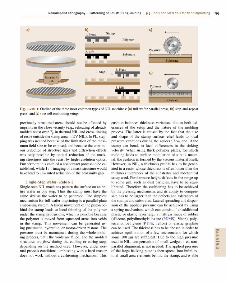
Nanoimprint Lithography – Patterning of Resists Using Molding 9.3 Tools and Materials for Nanoimprinting 293
1. Pressa)
2. Lift
Stamp
Polymer
Substrate
5. Lift
4. Press3. Step
Imprint +RIE
b)
Roller
Substrate
Roller
Substrate
c2)
c1)
Polymer
Polymer
Fig. 9.21a–c Outline of the three most common types of NIL machines: (a) full-wafer parallel press, (b) step-and-repeatpress, and (c) two roll-embossing setups
previously structured areas should not be affected byimprints in the close vicinity (e.g., reheating of alreadymolded resist over Tg in thermal NIL and cross-linkingof resist outside the stamp area in UV-NIL). In PL, step-ping was needed because of the limitation of the maxi-mum field size to be exposed, and because the continu-ous reduction of structure sizes and diffraction effectswas only possible by optical reduction of the mask-ing structures into the resist by high-resolution optics.Furthermore this enabled a noncontact process to be es-tablished, while 1 : 1 imaging of a mask structure wouldhave lead to unwanted reduction of the proximity gap.
Single-Step Wafer-Scale NILSingle-step NIL machines pattern the surface on an en-tire wafer in one step. Thus the stamp must have thesame size as the wafer to be patterned. The simplestmechanism for full wafer imprinting is a parallel-plateembossing system. A linear movement of the piston be-hind the stamp leads to local thinning of the polymerunder the stamp protrusions, which is possible becausethe polymer is moved from squeezed areas into voidsin the stamp. This movement can be generated us-ing pneumatic, hydraulic, or motor-driven pistons. Thepressure must be maintained during the whole mold-ing process, until the voids are filled, and the moldedstructures are fixed during the cooling or curing step,depending on the method used. However, under nor-mal process conditions, embossing with a hard masterdoes not work without a cushioning mechanism. This
cushion balances thickness variations due to both tol-erances of the setup and the nature of the moldingprocess. The latter is caused by the fact that the sizeand shape of the stamp surface relief leads to localpressure variations during the squeeze flow and, if thestamp can bend, to local differences in the sinkingvelocity. When using thick polymer plates, for whichmolding leads to surface modulation of a bulk mater-ial, the cushion is formed by the viscous material itself.However, in NIL, a thickness profile has to be gener-ated in a resist whose thickness is often lower than thethickness tolerances of the substrates and mechanicalsetup used. Furthermore height defects in the range upto some μm, such as dust particles, have to be equi-librated. Therefore the cushioning has to be achievedby the pressing mechanism, and its ability to compen-sate has to be larger than the defects and tolerances ofthe stamps and substrates. Lateral spreading and disper-sion of the applied pressure can be achieved by usinga spring mechanism, which can consist of an additionalplastic or elastic layer; e.g., a mattress made of rubber(silicone, polydimethylsiloxane (PDMS), Viton), poly-tetrafluoroethylene (PTFE, Teflon) or elastic graphitecan be used. The thickness has to be chosen in order toachieve equilibration of a few micrometers, for whichsome 100 μm are sufficient. Due to the high pressureused in NIL, compensation of small wedges, i. e., non-parallel alignment, is not needed. The applied pressureof the large backing plate is then spread into infinites-imal small area elements behind the stamp, and is able
PartA
9.3
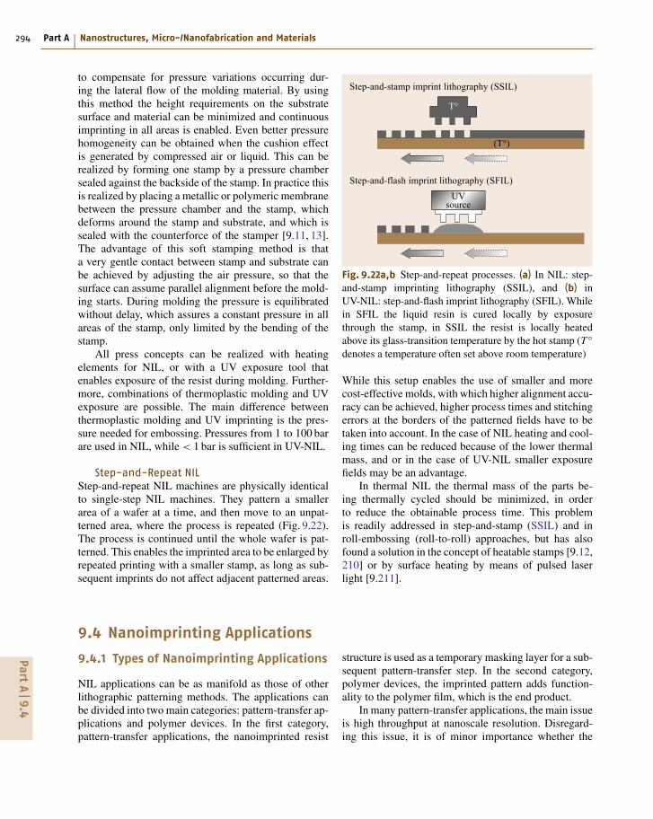
294 Part A Nanostructures, Micro-/Nanofabrication and Materials
to compensate for pressure variations occurring dur-ing the lateral flow of the molding material. By usingthis method the height requirements on the substratesurface and material can be minimized and continuousimprinting in all areas is enabled. Even better pressurehomogeneity can be obtained when the cushion effectis generated by compressed air or liquid. This can berealized by forming one stamp by a pressure chambersealed against the backside of the stamp. In practice thisis realized by placing a metallic or polymeric membranebetween the pressure chamber and the stamp, whichdeforms around the stamp and substrate, and which issealed with the counterforce of the stamper [9.11, 13].The advantage of this soft stamping method is thata very gentle contact between stamp and substrate canbe achieved by adjusting the air pressure, so that thesurface can assume parallel alignment before the mold-ing starts. During molding the pressure is equilibratedwithout delay, which assures a constant pressure in allareas of the stamp, only limited by the bending of thestamp.
All press concepts can be realized with heatingelements for NIL, or with a UV exposure tool thatenables exposure of the resist during molding. Further-more, combinations of thermoplastic molding and UVexposure are possible. The main difference betweenthermoplastic molding and UV imprinting is the pres-sure needed for embossing. Pressures from 1 to 100 barare used in NIL, while < 1 bar is sufficient in UV-NIL.
Step-and-Repeat NILStep-and-repeat NIL machines are physically identicalto single-step NIL machines. They pattern a smallerarea of a wafer at a time, and then move to an unpat-terned area, where the process is repeated (Fig. 9.22).The process is continued until the whole wafer is pat-terned. This enables the imprinted area to be enlarged byrepeated printing with a smaller stamp, as long as sub-sequent imprints do not affect adjacent patterned areas.
Step-and-stamp imprint lithography (SSIL)
Step-and-flash imprint lithography (SFIL)
(T°)
T°
UVsource
Fig. 9.22a,b Step-and-repeat processes. (a) In NIL: step-and-stamp imprinting lithography (SSIL), and (b) inUV-NIL: step-and-flash imprint lithography (SFIL). Whilein SFIL the liquid resin is cured locally by exposurethrough the stamp, in SSIL the resist is locally heatedabove its glass-transition temperature by the hot stamp (T ◦denotes a temperature often set above room temperature)
While this setup enables the use of smaller and morecost-effective molds, with which higher alignment accu-racy can be achieved, higher process times and stitchingerrors at the borders of the patterned fields have to betaken into account. In the case of NIL heating and cool-ing times can be reduced because of the lower thermalmass, and or in the case of UV-NIL smaller exposurefields may be an advantage.
In thermal NIL the thermal mass of the parts be-ing thermally cycled should be minimized, in orderto reduce the obtainable process time. This problemis readily addressed in step-and-stamp (SSIL) and inroll-embossing (roll-to-roll) approaches, but has alsofound a solution in the concept of heatable stamps [9.12,210] or by surface heating by means of pulsed laserlight [9.211].
9.4 Nanoimprinting Applications
9.4.1 Types of Nanoimprinting Applications
NIL applications can be as manifold as those of otherlithographic patterning methods. The applications canbe divided into two main categories: pattern-transfer ap-plications and polymer devices. In the first category,pattern-transfer applications, the nanoimprinted resist
structure is used as a temporary masking layer for a sub-sequent pattern-transfer step. In the second category,polymer devices, the imprinted pattern adds function-ality to the polymer film, which is the end product.
In many pattern-transfer applications, the main issueis high throughput at nanoscale resolution. Disregard-ing this issue, it is of minor importance whether the
PartA
9.4
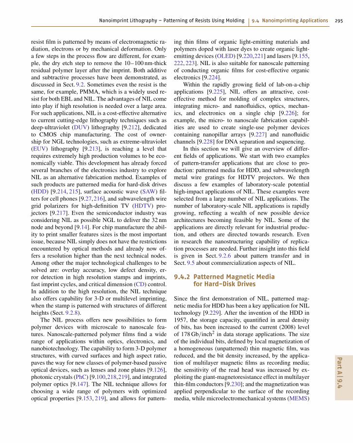
Nanoimprint Lithography – Patterning of Resists Using Molding 9.4 Nanoimprinting Applications 295
resist film is patterned by means of electromagnetic ra-diation, electrons or by mechanical deformation. Onlya few steps in the process flow are different, for exam-ple, the dry etch step to remove the 10–100 nm-thickresidual polymer layer after the imprint. Both additiveand subtractive processes have been demonstrated, asdiscussed in Sect. 9.2. Sometimes even the resist is thesame, for example, PMMA, which is a widely used re-sist for both EBL and NIL. The advantages of NIL comeinto play if high resolution is needed over a large area.For such applications, NIL is a cost-effective alternativeto current cutting-edge lithography techniques such asdeep-ultraviolet (DUV) lithography [9.212], dedicatedto CMOS chip manufacturing. The cost of owner-ship for NGL technologies, such as extreme-ultraviolet(EUV) lithography [9.213], is reaching a level thatrequires extremely high production volumes to be eco-nomically viable. This development has already forcedseveral branches of the electronics industry to exploreNIL as an alternative fabrication method. Examples ofsuch products are patterned media for hard-disk drives(HDD) [9.214, 215], surface acoustic wave (SAW) fil-ters for cell phones [9.27,216], and subwavelength wiregrid polarizers for high-definition TV (HDTV) pro-jectors [9.217]. Even the semiconductor industry wasconsidering NIL as possible NGL to deliver the 32 nmnode and beyond [9.14]. For chip manufacture the abil-ity to print smaller features sizes is the most importantissue, because NIL simply does not have the restrictionsencountered by optical methods and already now of-fers a resolution higher than the next technical nodes.Among other the major technological challenges to besolved are: overlay accuracy, low defect density, er-ror detection in high resolution stamps and imprints,fast imprint cycles, and critical dimension (CD) control.In addition to the high resolution, the NIL techniquealso offers capability for 3-D or multilevel imprinting,when the stamp is patterned with structures of differentheights (Sect. 9.2.8).
The NIL process offers new possibilities to formpolymer devices with microscale to nanoscale fea-tures. Nanoscale-patterned polymer films find a widerange of applications within optics, electronics, andnanobiotechnology. The capability to form 3-D polymerstructures, with curved surfaces and high aspect ratio,paves the way for new classes of polymer-based passiveoptical devices, such as lenses and zone plates [9.126],photonic crystals (PhC) [9.100,218,219], and integratedpolymer optics [9.147]. The NIL technique allows forchoosing a wide range of polymers with optimizedoptical properties [9.153, 219], and allows for pattern-
ing thin films of organic light-emitting materials andpolymers doped with laser dyes to create organic light-emitting devices (OLED) [9.220,221] and lasers [9.155,222, 223]. NIL is also suitable for nanoscale patterningof conducting organic films for cost-effective organicelectronics [9.224].
Within the rapidly growing field of lab-on-a-chipapplications [9.225], NIL offers an attractive, cost-effective method for molding of complex structures,integrating micro- and nanofluidics, optics, mechan-ics, and electronics on a single chip [9.226]; forexample, the micro- to nanoscale fabrication capabil-ities are used to create single-use polymer devicescontaining nanopillar arrays [9.227] and nanofluidicchannels [9.228] for DNA separation and sequencing.
In this section we will give an overview of differ-ent fields of applications. We start with two examplesof pattern-transfer applications that are close to pro-duction: patterned media for HDD, and subwavelengthmetal wire gratings for HDTV projectors. We thendiscuss a few examples of laboratory-scale potentialhigh-impact applications of NIL. These examples wereselected from a large number of NIL applications. Thenumber of laboratory-scale NIL applications is rapidlygrowing, reflecting a wealth of new possible devicearchitectures becoming feasible by NIL. Some of theapplications are directly relevant for industrial produc-tion, and others are directed towards research. Evenin research the nanostructuring capability of replica-tion processes are needed. Further insight into this fieldis given in Sect. 9.2.6 about pattern transfer and inSect. 9.5 about commercialization aspects of NIL.
9.4.2 Patterned Magnetic Mediafor Hard-Disk Drives
Since the first demonstration of NIL, patterned mag-netic media for HDD has been a key application for NILtechnology [9.229]. After the invention of the HDD in1957, the storage capacity, quantified in areal densityof bits, has been increased to the current (2008) levelof 178 Gb/inch2 in data storage applications. The sizeof the individual bits, defined by local magnetization ofa homogeneous (unpatterned) thin magnetic film, wasreduced, and the bit density increased, by the applica-tion of multilayer magnetic films as recording media;the sensitivity of the read head was increased by ex-ploiting the giant-magnetoresistance effect in multilayerthin-film conductors [9.230]; and the magnetization wasapplied perpendicular to the surface of the recordingmedia, while microelectromechanical systems (MEMS)
PartA
9.4
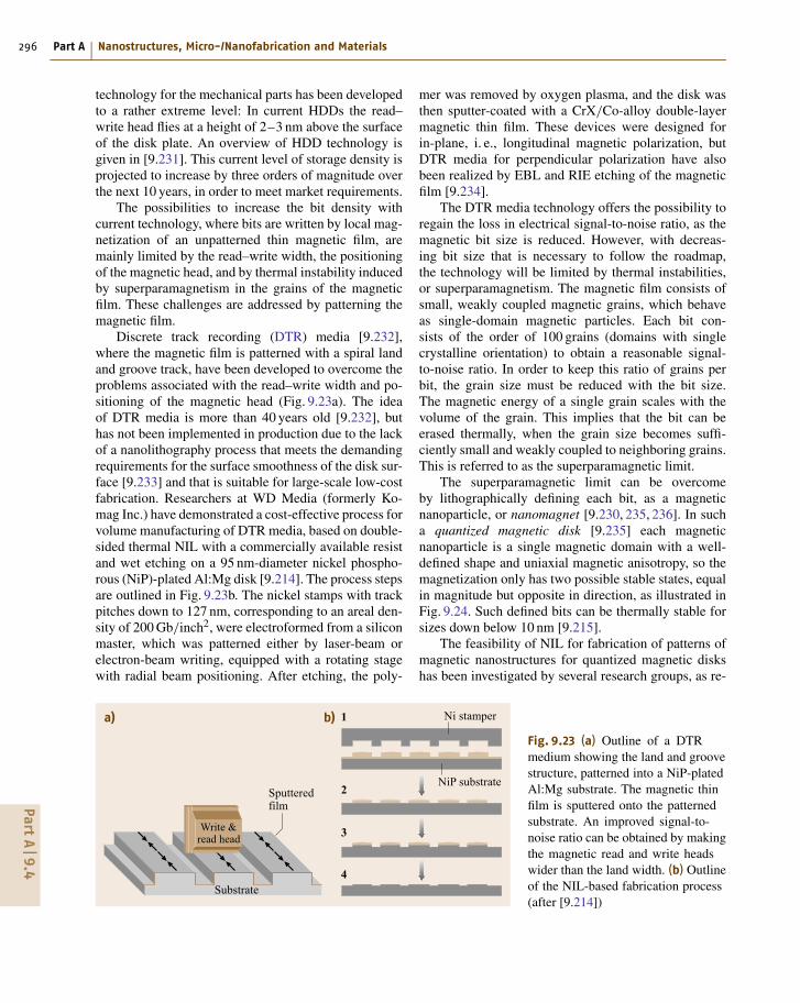
296 Part A Nanostructures, Micro-/Nanofabrication and Materials
technology for the mechanical parts has been developedto a rather extreme level: In current HDDs the read–write head flies at a height of 2–3 nm above the surfaceof the disk plate. An overview of HDD technology isgiven in [9.231]. This current level of storage density isprojected to increase by three orders of magnitude overthe next 10 years, in order to meet market requirements.
The possibilities to increase the bit density withcurrent technology, where bits are written by local mag-netization of an unpatterned thin magnetic film, aremainly limited by the read–write width, the positioningof the magnetic head, and by thermal instability inducedby superparamagnetism in the grains of the magneticfilm. These challenges are addressed by patterning themagnetic film.
Discrete track recording (DTR) media [9.232],where the magnetic film is patterned with a spiral landand groove track, have been developed to overcome theproblems associated with the read–write width and po-sitioning of the magnetic head (Fig. 9.23a). The ideaof DTR media is more than 40 years old [9.232], buthas not been implemented in production due to the lackof a nanolithography process that meets the demandingrequirements for the surface smoothness of the disk sur-face [9.233] and that is suitable for large-scale low-costfabrication. Researchers at WD Media (formerly Ko-mag Inc.) have demonstrated a cost-effective process forvolume manufacturing of DTR media, based on double-sided thermal NIL with a commercially available resistand wet etching on a 95 nm-diameter nickel phospho-rous (NiP)-plated Al:Mg disk [9.214]. The process stepsare outlined in Fig. 9.23b. The nickel stamps with trackpitches down to 127 nm, corresponding to an areal den-sity of 200 Gb/inch2, were electroformed from a siliconmaster, which was patterned either by laser-beam orelectron-beam writing, equipped with a rotating stagewith radial beam positioning. After etching, the poly-
Substrate
1
Write &read head
Sputteredfilm
NiP substrate
Ni stamper
2
3
4
a) b)
Fig. 9.23 (a) Outline of a DTRmedium showing the land and groovestructure, patterned into a NiP-platedAl:Mg substrate. The magnetic thinfilm is sputtered onto the patternedsubstrate. An improved signal-to-noise ratio can be obtained by makingthe magnetic read and write headswider than the land width. (b) Outlineof the NIL-based fabrication process(after [9.214])
mer was removed by oxygen plasma, and the disk wasthen sputter-coated with a CrX/Co-alloy double-layermagnetic thin film. These devices were designed forin-plane, i. e., longitudinal magnetic polarization, butDTR media for perpendicular polarization have alsobeen realized by EBL and RIE etching of the magneticfilm [9.234].
The DTR media technology offers the possibility toregain the loss in electrical signal-to-noise ratio, as themagnetic bit size is reduced. However, with decreas-ing bit size that is necessary to follow the roadmap,the technology will be limited by thermal instabilities,or superparamagnetism. The magnetic film consists ofsmall, weakly coupled magnetic grains, which behaveas single-domain magnetic particles. Each bit con-sists of the order of 100 grains (domains with singlecrystalline orientation) to obtain a reasonable signal-to-noise ratio. In order to keep this ratio of grains perbit, the grain size must be reduced with the bit size.The magnetic energy of a single grain scales with thevolume of the grain. This implies that the bit can beerased thermally, when the grain size becomes suffi-ciently small and weakly coupled to neighboring grains.This is referred to as the superparamagnetic limit.
The superparamagnetic limit can be overcomeby lithographically defining each bit, as a magneticnanoparticle, or nanomagnet [9.230, 235, 236]. In sucha quantized magnetic disk [9.235] each magneticnanoparticle is a single magnetic domain with a well-defined shape and uniaxial magnetic anisotropy, so themagnetization only has two possible stable states, equalin magnitude but opposite in direction, as illustrated inFig. 9.24. Such defined bits can be thermally stable forsizes down below 10 nm [9.215].
The feasibility of NIL for fabrication of patterns ofmagnetic nanostructures for quantized magnetic diskshas been investigated by several research groups, as re-
PartA
9.4

Nanoimprint Lithography – Patterning of Resists Using Molding 9.4 Nanoimprinting Applications 297
cently reviewed in [9.237–239]. The imprinted patternhas been transformed to magnetic nanoparticles by elec-troplating into etched holes [9.99], by lift-off [9.240],and by deposition onto etched pillars [9.215, 241].
In Fig. 9.25 we show the outline of the process flowfor large-area fabrication of 55 nm-diameter, 11 nm-high CoPt magnetic islands [9.215], by means ofUV-NIL. A SiO2 master containing three 50 × 50 μm2
areas of hexagonal 100 nm-pitch array of 30 nm-high,55 nm-diameter pillars was fabricated by defining thedot pattern by means of EBL in a 160 nm-thick filmof Mw 950 k PMMA. The patterned PMMA film wasused in a lift-off process, to define a Cr etch mask.The pillars were etched by tetrafluoromethane (CF4)RIE, and the metal mask was removed. The masterwas used to form a stamp in a photopolymer mater-ial. This stamp is used to UV-imprint the dot patternin a photopolymer film on a SiO2 substrate, leavinga replica in the photocured polymer, with 28 nm-high pillars on top of a 10 nm-thick residual layer.The pattern was transferred to the SiO2 substrate byCF4 RIE to remove the residual layer, followed bya (7 : 1)/(CF4 : CH4) RIE. Finally a CoPt magneticmultilayer structure (Pt1 nm(Co0.3 nmPt1 nm)7Pt1 nm) wasdeposited by electron-beam evaporation. The deviceswere characterized by magnetic force microscopy(MFM), revealing that the film on each pillar isa magnetically isolated single domain that switchesindependently.
9.4.3 Subwavelength Metal-Strip Gratings
Metallic wire gratings with a period below 200 nm canbe used to create polarizers, polarization beam splitters,and optical isolators in the visible range. Such deviceshave many applications in compact and integrated op-tics. One example is the use of subwavelength wire-grid
SEM
Make masterby e-beamlithography
SiO2
1µm
Form stampby photo-polymerization
SiO2
Form replicaby photo-polymerization
SEM Photo-polymer
SEM AFM
Transfer patternby reactive ionetching
MFM
CoPt
Evaporatemagneticfilm
Fig. 9.25 Outline of the process flowfor fabrication of 55 nm diametermagnetic islands by UV-NIL. The toppanel shows SEM, AFM, and MFMmicrographs at the different stagesof the process. The MFM micro-graph shows quantized up and downmagnetization of isolated domains.Reproduced from [9.215]
Nonmagnetic
MagneticSN
S
N
NS
Substrate
N
S
S
N
S
N
Fig. 9.24 Outline of a patterned magnetic disk for high-densitydata storage. Each bit is a lithographically defined, single-domainmagnetic nanostructure, embedded in a nonmagnetic matrix (af-ter [9.229])
polarization beam splitters in liquid crystal on silicon(LCoS) projection displays for HDTV, yielding highercontrast, uniformity, and brightness of the displayed im-age (Fig. 9.26).
The polarizing functionality of subwavelength wiregratings is based on form birefringence, an opticalanisotropy which appears when isotropic material isstructured on a length scale much smaller than the wave-length of light λ. In this limit, the description of lightpropagation based on the laws of diffraction, refraction,and reflection is not valid, and a rigorous solution ofMaxwell’s equations with the relevant boundary condi-tions must be applied. For a review of subwavelengthoptics see [9.242]. The subwavelength linear grating ofperiod d < λ/2, line width a, and height h, as illustratedin Fig. 9.27, will behave as a film of birefringent mater-ial with refractive indices ns and np for the s-polarized(E-field parallel to the grating) and p-polarized (E-field
PartA
9.4
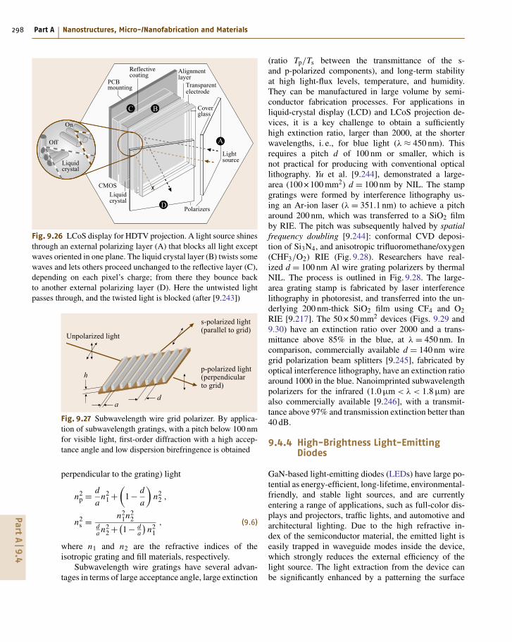
298 Part A Nanostructures, Micro-/Nanofabrication and Materials
Coverglass
Reflectivecoating
B
PCBmounting
Alignmentlayer
Transparentelectrode
C
A
D
CMOSLiquidcrystal
Polarizers
Lightsource
On
Off
Liquidcrystal
C
A
D
B
Fig. 9.26 LCoS display for HDTV projection. A light source shinesthrough an external polarizing layer (A) that blocks all light exceptwaves oriented in one plane. The liquid crystal layer (B) twists somewaves and lets others proceed unchanged to the reflective layer (C),depending on each pixel’s charge; from there they bounce backto another external polarizing layer (D). Here the untwisted lightpasses through, and the twisted light is blocked (after [9.243])
s-polarized light(parallel to grid)
hp-polarized light(perpendicularto grid)
Unpolarized light
ad
Fig. 9.27 Subwavelength wire grid polarizer. By applica-tion of subwavelength gratings, with a pitch below 100 nmfor visible light, first-order diffraction with a high accep-tance angle and low dispersion birefringence is obtained
perpendicular to the grating) light
n2p = d
an2
1 +(
1− d
a
)
n22 ,
n2s = n2
1n22
da n2
2 + (1− d
a
)n2
1
, (9.6)
where n1 and n2 are the refractive indices of theisotropic grating and fill materials, respectively.
Subwavelength wire gratings have several advan-tages in terms of large acceptance angle, large extinction
(ratio Tp/Ts between the transmittance of the s-and p-polarized components), and long-term stabilityat high light-flux levels, temperature, and humidity.They can be manufactured in large volume by semi-conductor fabrication processes. For applications inliquid-crystal display (LCD) and LCoS projection de-vices, it is a key challenge to obtain a sufficientlyhigh extinction ratio, larger than 2000, at the shorterwavelengths, i. e., for blue light (λ ≈ 450 nm). Thisrequires a pitch d of 100 nm or smaller, which isnot practical for producing with conventional opticallithography. Yu et al. [9.244], demonstrated a large-area (100 × 100 mm2) d = 100 nm by NIL. The stampgratings were formed by interference lithography us-ing an Ar-ion laser (λ = 351.1 nm) to achieve a pitcharound 200 nm, which was transferred to a SiO2 filmby RIE. The pitch was subsequently halved by spatialfrequency doubling [9.244]: conformal CVD deposi-tion of Si3N4, and anisotropic trifluoromethane/oxygen(CHF3/O2) RIE (Fig. 9.28). Researchers have real-ized d = 100 nm Al wire grating polarizers by thermalNIL. The process is outlined in Fig. 9.28. The large-area grating stamp is fabricated by laser interferencelithography in photoresist, and transferred into the un-derlying 200 nm-thick SiO2 film using CF4 and O2RIE [9.217]. The 50 × 50 mm2 devices (Figs. 9.29 and9.30) have an extinction ratio over 2000 and a trans-mittance above 85% in the blue, at λ = 450 nm. Incomparison, commercially available d = 140 nm wiregrid polarization beam splitters [9.245], fabricated byoptical interference lithography, have an extinction ratioaround 1000 in the blue. Nanoimprinted subwavelengthpolarizers for the infrared (1.0 μm < λ < 1.8 μm) arealso commercially available [9.246], with a transmit-tance above 97% and transmission extinction better than40 dB.
9.4.4 High-Brightness Light-EmittingDiodes
GaN-based light-emitting diodes (LEDs) have large po-tential as energy-efficient, long-lifetime, environmental-friendly, and stable light sources, and are currentlyentering a range of applications, such as full-color dis-plays and projectors, traffic lights, and automotive andarchitectural lighting. Due to the high refractive in-dex of the semiconductor material, the emitted light iseasily trapped in waveguide modes inside the device,which strongly reduces the external efficiency of thelight source. The light extraction from the device canbe significantly enhanced by a patterning the surface
PartA
9.4

Nanoimprint Lithography – Patterning of Resists Using Molding 9.4 Nanoimprinting Applications 299
Imprint (heatand pressure)
Aluminumdeposition
Resist coating
Demolding
Stamp fabrication bylaser interference lithography
Residual layerremoving
Aluminum RIE
Fig. 9.28 Outline of the NIL pro-cess to fabricate d = 100 nm-pitchaluminum wire grating polarizers
Fig. 9.29 Subwavelength wire grating polarizer with d =100 nm pitch. The aluminum ribs are 100 nm high
with a 2-D photonic crystal [9.247, 248] – an array ofholes – with a photonic bandgap that prohibits prop-agation of photons of frequencies within the bandgap,leading to enhanced extraction of photons through thesurface of the device. Kim et al. [9.248] demonstrateda ninefold enhancement of photoluminescence inten-sity of GaN-based green LEDs by means of a 2-D PhCstructures of 180 nm-diameter, 100 nm-deep holes ar-ranged in a square lattice with a period of 295 nm. ThePhC pattern was defined by thermal NIL and RIE etch-ing through a Cr mask. The NIL stamp was patternedby laser interference lithography.
Fig. 9.30 Large-area 100 nm-pitchwire grid polarizer with 85% trans-mission and extinction ratio largerthan 2000 at wavelength λ = 450 nm(blue light)
9.4.5 Polymer Optics
NIL is ideally suited for the fabrication of polymernanophotonics and waveguide devices with submicroncritical dimensions, defined over large areas. It is alsocompatible with many polymer materials, giving greatfreedom to choose a material with specific optical prop-erties [9.222, 223, 249].
In Fig. 9.31 we show a polymer microring resonatorfabricated by NIL [9.147]. This type of device has beenrealized in PMMA, PC, and PS on SiO2 substrates.The resonator consists of a planar waveguide and anadjacent microring waveguide. The waveguide and mi-croring are coupled though the evanescent field in thecoupling region. Resonant dips in the transmissionthrough the waveguide occur when the phase pick-upin a trip round the microring is equal to 2πm, where mis an integer. The device works as a narrow-bandwidthfilter, and finds applications within integrated optics andfor biosensing [9.47].
The evanescent coupling coefficient between thewaveguide and microring depends exponentially onthe size of the gap. The devices are realized with1.5 μm-high waveguides, and a coupling air-gap of100–200 nm. The process flow is outlined in Fig. 9.31c.A thin initial polymer layer is spin-cast onto a SiO2 sub-strate layer. The stamp has a very large fill factor and
PartA
9.4
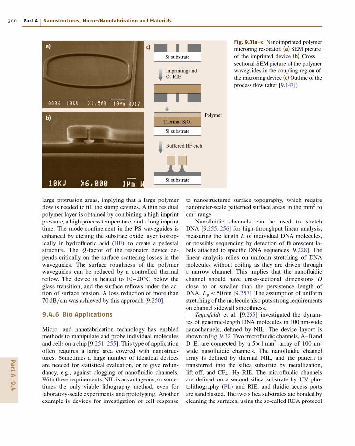
300 Part A Nanostructures, Micro-/Nanofabrication and Materials
a) c)
b)
Si substrate
Si substrate
Thermal SiO2
Si substrate
Imprinting andO2 RIE
Buffered HF etch
Polymer
Fig. 9.31a–c Nanoimprinted polymermicroring resonator. (a) SEM pictureof the imprinted device (b) Crosssectional SEM picture of the polymerwaveguides in the coupling region ofthe microring device (c) Outline of theprocess flow (after [9.147])
large protrusion areas, implying that a large polymerflow is needed to fill the stamp cavities. A thin residualpolymer layer is obtained by combining a high imprintpressure, a high process temperature, and a long imprinttime. The mode confinement in the PS waveguides isenhanced by etching the substrate oxide layer isotrop-ically in hydrofluoric acid (HF), to create a pedestalstructure. The Q-factor of the resonator device de-pends critically on the surface scattering losses in thewaveguides. The surface roughness of the polymerwaveguides can be reduced by a controlled thermalreflow. The device is heated to 10–20 ◦C below theglass transition, and the surface reflows under the ac-tion of surface tension. A loss reduction of more than70 dB/cm was achieved by this approach [9.250].
9.4.6 Bio Applications
Micro- and nanofabrication technology has enabledmethods to manipulate and probe individual moleculesand cells on a chip [9.251–255]. This type of applicationoften requires a large area covered with nanostruc-tures. Sometimes a large number of identical devicesare needed for statistical evaluation, or to give redun-dancy, e.g., against clogging of nanofluidic channels.With these requirements, NIL is advantageous, or some-times the only viable lithography method, even forlaboratory-scale experiments and prototyping. Anotherexample is devices for investigation of cell response
to nanostructured surface topography, which requirenanometer-scale patterned surface areas in the mm2 tocm2 range.
Nanofluidic channels can be used to stretchDNA [9.255, 256] for high-throughput linear analysis,measuring the length L of individual DNA molecules,or possibly sequencing by detection of fluorescent la-bels attached to specific DNA sequences [9.228]. Thelinear analysis relies on uniform stretching of DNAmolecules without coiling as they are driven througha narrow channel. This implies that the nanofluidicchannel should have cross-sectional dimensions Dclose to or smaller than the persistence length ofDNA, Lp ≈ 50 nm [9.257]. The assumption of uniformstretching of the molecule also puts strong requirementson channel sidewall smoothness.
Tegenfeldt et al. [9.255] investigated the dynam-ics of genomic-length DNA molecules in 100 nm-widenanochannels, defined by NIL. The device layout isshown in Fig. 9.32. Two microfluidic channels, A–B andD–E, are connected by a 5 × 1 mm2 array of 100 nm-wide nanofluidic channels. The nanofluidic channelarray is defined by thermal NIL, and the pattern istransferred into the silica substrate by metallization,lift-off, and CF4 : H2 RIE. The microfluidic channelsare defined on a second silica substrate by UV pho-tolithography (PL) and RIE, and fluidic access portsare sandblasted. The two silica substrates are bonded bycleaning the surfaces, using the so-called RCA protocol
PartA
9.4
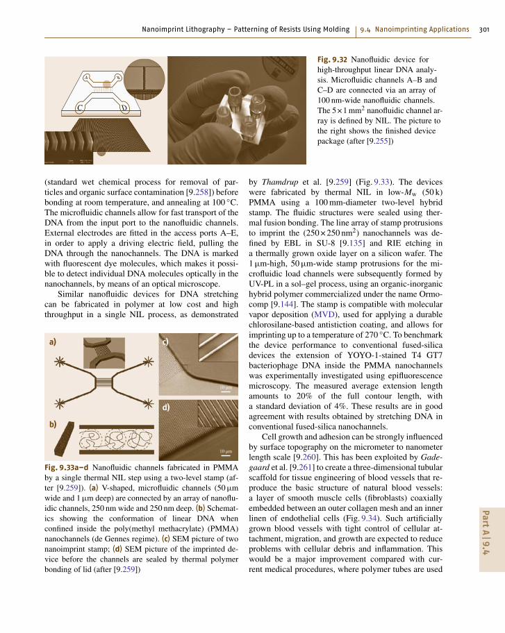
Nanoimprint Lithography – Patterning of Resists Using Molding 9.4 Nanoimprinting Applications 301
Fig. 9.32 Nanofluidic device forhigh-throughput linear DNA analy-sis. Microfluidic channels A–B andC–D are connected via an array of100 nm-wide nanofluidic channels.The 5 × 1 mm2 nanofluidic channel ar-ray is defined by NIL. The picture tothe right shows the finished devicepackage (after [9.255])
(standard wet chemical process for removal of par-ticles and organic surface contamination [9.258]) beforebonding at room temperature, and annealing at 100 ◦C.The microfluidic channels allow for fast transport of theDNA from the input port to the nanofluidic channels.External electrodes are fitted in the access ports A–E,in order to apply a driving electric field, pulling theDNA through the nanochannels. The DNA is markedwith fluorescent dye molecules, which makes it possi-ble to detect individual DNA molecules optically in thenanochannels, by means of an optical microscope.
Similar nanofluidic devices for DNA stretchingcan be fabricated in polymer at low cost and highthroughput in a single NIL process, as demonstrated
a)
b)
c)
d)
10 µm
10 µm
Fig. 9.33a–d Nanofluidic channels fabricated in PMMAby a single thermal NIL step using a two-level stamp (af-ter [9.259]). (a) V-shaped, microfluidic channels (50 μmwide and 1 μm deep) are connected by an array of nanoflu-idic channels, 250 nm wide and 250 nm deep. (b) Schemat-ics showing the conformation of linear DNA whenconfined inside the poly(methyl methacrylate) (PMMA)nanochannels (de Gennes regime). (c) SEM picture of twonanoimprint stamp; (d) SEM picture of the imprinted de-vice before the channels are sealed by thermal polymerbonding of lid (after [9.259])
by Thamdrup et al. [9.259] (Fig. 9.33). The deviceswere fabricated by thermal NIL in low-Mw (50 k)PMMA using a 100 mm-diameter two-level hybridstamp. The fluidic structures were sealed using ther-mal fusion bonding. The line array of stamp protrusionsto imprint the (250 × 250 nm2) nanochannels was de-fined by EBL in SU-8 [9.135] and RIE etching ina thermally grown oxide layer on a silicon wafer. The1 μm-high, 50 μm-wide stamp protrusions for the mi-crofluidic load channels were subsequently formed byUV-PL in a sol–gel process, using an organic-inorganichybrid polymer commercialized under the name Ormo-comp [9.144]. The stamp is compatible with molecularvapor deposition (MVD), used for applying a durablechlorosilane-based antistiction coating, and allows forimprinting up to a temperature of 270 ◦C. To benchmarkthe device performance to conventional fused-silicadevices the extension of YOYO-1-stained T4 GT7bacteriophage DNA inside the PMMA nanochannelswas experimentally investigated using epifluorescencemicroscopy. The measured average extension lengthamounts to 20% of the full contour length, witha standard deviation of 4%. These results are in goodagreement with results obtained by stretching DNA inconventional fused-silica nanochannels.
Cell growth and adhesion can be strongly influencedby surface topography on the micrometer to nanometerlength scale [9.260]. This has been exploited by Gade-gaard et al. [9.261] to create a three-dimensional tubularscaffold for tissue engineering of blood vessels that re-produce the basic structure of natural blood vessels:a layer of smooth muscle cells (fibroblasts) coaxiallyembedded between an outer collagen mesh and an innerlinen of endothelial cells (Fig. 9.34). Such artificiallygrown blood vessels with tight control of cellular at-tachment, migration, and growth are expected to reduceproblems with cellular debris and inflammation. Thiswould be a major improvement compared with cur-rent medical procedures, where polymer tubes are used
PartA
9.4
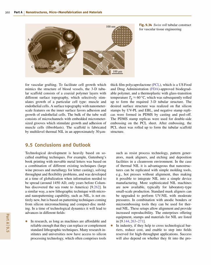
302 Part A Nanostructures, Micro-/Nanofabrication and Materials
100 nm
100 µm
A, B
C
D
F
E
Fig. 9.34 Swiss roll tubular constructfor vascular tissue engineering
for vascular grafting. To facilitate cell growth whichmimics the structure of blood vessels, the 3-D tubu-lar scaffold consists of a coaxial polymer layers withdifferent surface topography, which selectively stim-ulates growth of a particular cell type: muscle andendothelial cells. A surface topography with nanometer-scale features on the inner surface favors adhesion andgrowth of endothelial cells. The bulk of the tube wallconsists of microchannels with embedded micrometer-sized grooves which stimulate growth and adhesion ofmuscle cells (fibroblasts). The scaffold is fabricatedby multilevel thermal NIL in an approximately 30 μm-
thick film polycaprolactone (PCL), which is a US Foodand Drug Administration (FDA)-approved biodegrad-able polymer, and a thermoplastic with glass-transitiontemperature Tg ≈ 60 ◦C, which was subsequently rolledup to form the required 3-D tubular structure. Thedesired surface structure was realized on flat siliconstamps by UV-PL and EBL, and negative stamp repli-cas were formed in PDMS by casting and peel-off.The PDMS stamp replicas were used for double-sideembossing on the PCL sheet. After embossing, thePCL sheet was rolled up to form the tubular scaffoldstructure.
9.5 Conclusions and Outlook
Technological development is heavily based on so-called enabling techniques. For example, Gutenberg’sbook printing with movable metal letters was based ona combination of different existing techniques (largewine presses and metallurgy for letter casting), solvingthroughput and flexibility problems, and was developedat a time of globalization when information needed tobe spread (around 1450 AD, only years before Colum-bus discovered the sea route to America) [9.262]. Ina similar way, a new lithographic technique with micro-and nanopatterning capability, such as NIL, is not en-tirely new, but is based on patterning techniques comingfrom silicon micromachining and compact-disc mold-ing. In a time of technological dynamics it will lead toadvances in different fields:
• In research, as long as machines are affordable andreliable enough that they can replace or complementstandard lithographic techniques. Many research in-stitutes and universities now have access to siliconprocessing technology, which often comprises tools
such as resist process technology, pattern gener-ators, mask aligners, and etching and depositionfacilities in a cleanroom environment. In the caseof thermal NIL it is advantageous that nanostruc-tures can be replicated with simple molding tools,e.g., hot presses without alignment, thus makingit possible to integrate NIL into a simple devicemanufacturing. More sophisticated NIL machinesare now available, typically for laboratory-typesmall-scale production. Standard mask aligners canbe upgraded to perform UV-NIL with moderatepressures. In combination with anodic bonders ormicroembossing tools they can be used for ther-mal NIL. These setups allow alignment and provideincreased reproducibility. The enterprises offeringequipment, stamps and materials for NIL are listedin [9.144, 263–271].• In industry, if they help to cross technological bar-riers, reduce cost, and enable to step into fieldsreserved for high-throughput applications. Successwill also depend on whether they fit into the pro-
PartA
9.5

Nanoimprint Lithography – Patterning of Resists Using Molding 9.5 Conclusions and Outlook 303
cess chain already established in a silicon cleanroomenvironment. Furthermore substrate sizes, through-put, and yield have to correspond to the productionneeds. As in research, many of the machines alreadyavailable can be used for moderate-scale produc-tion. They can be scaled up to substrate sizes of200 mm and higher in combination with batch-modeoperation. More sophisticated are machines basedon step-and-repeat NIL, which can help to solveequilibration and overlay issues. Further improve-ments can be expected if new resists and processschemes are developed. In order to achieve a criti-cal mass of technological expertise, the integrationof NIL into a consortium of technology providers isof advantage, making it possible for manufacturersto buy standard equipment and materials, along withprocess knowhow.
Until now NIL was considered as a very promis-ing patterning method, because it combines resolutionwith large area and throughput. As long as it is seenas an alternative to establish high-end photolithogra-phies, the strategy will most likely be to replacesingle lithographic steps by imprinting. The only con-sequence in the multimasking process sequence neededin microchip fabrication would then be modifying thepattern transfer process, e.g., by adding the resid-ual layer etch (Sect. 9.2.6). The requirements of theITRS roadmap are so high that other more estab-lished NGLs might make faster advances towards thenext node, and the introduction of NIL into large-scale fabrication would be further postponed (NILwas first added to the 2003 ITRS roadmap for the32 nm node [9.14, 272]). However, NIL has other ca-pabilities, as demonstrated in Sect. 9.4, even if notall requirements of the ITRS roadmap are met atonce:
• Enterprises with applications ranging from tem-plates for hard-disk production to SAW filters formobile phones, polarizers for flat-panel screens, andtemplates for biodevices are now heading into repli-cation techniques based on NIL processes. Most ofthese processes are based on single layers coveredwith nanostructures, mostly regular high-resolutiongratings and dot arrays, and need single-step wafer-scale replication tools for large areas.
• The 3-D patterning capability (Sect. 9.2.8) makes itpossible to develop innovative pattern-transfer pro-cesses, thus leading to significant cost reduction.Similar advances could be achieved if materials withnew properties are patterned. This is mainly due tothe fact that NIL has the concept of displacing ma-terial at the nanoscale rather than removing materialselectively and locally. Often this goes along withsome tradeoffs on resolution and alignment, whichis justified depending on the application.
NIL has now passed a barrier from the laboratoryscale to industrial preproduction. Although it seemsthat room-temperature processes based on UV exposurehave an advantage over processes based on thermo-cycles, to date it is difficult to say which processwill become a standard process and make it to theproduction line. For example, isothermal processes atelevated temperatures using hybrid processes that useboth thermal NIL and hardening by UV curing havebeen established [9.273]. With state-of-the-art UV-NILequipment [9.268], more than six wafers per hour witha diameter of 200 mm can now be achieved in a step-and-repeat modus (using a stamp area of 45 × 60 mm2).Single-step wafer-scale hot embossing has similar capa-bilities, and can even push throughput further if heatablestamps with low thermal mass are used [9.210, 274].However, NIL is currently such a fast-moving field thatprejudgment about the final success of one technique isnot possible or advisable. Innovative solutions are stillneeded to solve process and stamp lifetime issues formany different applications. Probably, not only a sin-gle NIL process will be successfully implemented, butmany variants of NIL. This includes hybrid approaches,e.g., NIL in combination with other lithographic pro-cesses, or the fabrication and copying of stamps usingNIL.
The aim of this chapter was to give an insight intothe concepts used in NIL, along with presenting the ad-vantages and limitations of processes ranging from toolfabrication to pattern transfer. Although more referringto the older thermoplastic molding process, which isthe authors’ original field of expertise, it was intendedto be general enough that future developments can bejudged. The interested reader, however, will find moredetailed information at technological conferences and inscientific publications, and also in the patent literature.
PartA
9.5
304 Part A Nanostructures, Micro-/Nanofabrication and Materials
References
9.1 E. Berliner: Gramophone, US Patent 372786 (1887),http://www.audioannals.com/berlinere.htm
9.2 E. Berliner: Process for producing records of sound,US Patent 382790 (1888), http://www.audioannals.com/berlinere.htm
9.3 J.C. Ruda: Record manufacturing: making sound foreveryone, J. Audio Eng. Soc. 25(10/11), 702–711 (1977)
9.4 K.C. Pohlmann: The Compact Disc Handbook, Com-put. Music Dig. Audio Ser., Vol. 5, 2nd edn. (A-REditions, Madison 1992)
9.5 H. Schift, C. David, M. Gabriel, J. Gobrecht,L.J. Heyderman, W. Kaiser, S. Köppel, L. Scandella:Nanoreplication in polymers using hot embossingand injection molding, Microelectron. Eng. 53, 171–174 (2000)
9.6 S.Y. Chou, P.R. Krauss: Imprint lithography withsub-10 nm feature size and high throughput, Mi-croelectron. Eng. 35, 237–240 (1997)
9.7 R.W. Jaszewski, H. Schift, J. Gobrecht, P. Smith: Hotembossing in polymers as a direct way to patternresist, Microelectron. Eng. 41/42, 575–578 (1998)
9.8 Y. Xia, G.M. Whitesides: Soft lithography, Angew.Chem. Int. Ed. 37, 550–575 (1998)
9.9 B. Michel, A. Bernard, A. Bietsch, E. Delamarche,M. Geissler, D. Juncker, H. Kind, J.-P. Renault,H. Rothuizen, H. Schmid, P. Schmidt-Winkel,R. Stutz, H. Wolf: Printing meets lithography: Softapproaches to high-resolution, IBM J. Res. Dev.45(5), 697–719 (2001)
9.10 W. Menz, J. Mohr, O. Paul: Microsystem Technology(Wiley-VCH, Weinheim 2001)
9.11 H. Schift: Nanoimprint lithography: An old story inmodern times? A review, J. Vac. Sci. Technol. B 26(2),458–480 (2008)
9.12 H. Schift (Ed.): NaPa Library of Processes (NaPa-consortium, 2008), http://www.napanil.org (lastaccess December 2009)
9.13 C. Sotomayor Torres: Alternative lithography –Unleashing the potential of nanotechnology. In:Nanostructure Science and Technology, ed. byD.J. Lockwood (Kluwer, New York 2003)
9.14 International Technology Roadmap for Semiconduc-tors, http://public.itrs.net/ (last accessed May 8,2008)
9.15 R. Compaño (Ed.): Technology Roadmap for Nano-electronics, European Commission IST Programme,Future and Emerging Technologies, 2nd edn. (Eu-ropean Commission, Brussels 2000)
9.16 H. Moore: Cramming more components onto inte-grated circuits, Electronics 38(8), 114–117 (1965)
9.17 S. Okazaki: Resolution limits of optical lithography,J. Vac. Sci. Technol. B 9(6), 2829–2833 (1991)
9.18 L.J. Heyderman, H. Schift, C. David, J. Gobrecht,T. Schweizer: Flow behaviour of thin polymer films
used for hot embossing lithography, Microelectron.Eng. 54, 229–245 (2000)
9.19 H. Schulz, M. Wissen, N. Bogdanski, H.-C. Scheer,K. Mattes, C. Friedrich: Impact of molecular weightof polymers and shear rate effects for nanoimprintlithography, Microelectron. Eng. 83, 259–280 (2006)
9.20 S.Y. Chou, P.R. Krauss, P.J. Renstrom: Imprint of sub-25 nm vias and trenches in polymers, Appl. Phys.Lett. 67(21), 3114–3116 (1995)
9.21 S.Y. Chou, P.R. Krauss, P.J. Renstrom: Nanoimprintlithography, J. Vac. Sci. Technol. B 14(6), 4129–4133(1996)
9.22 S.Y. Chou: Nanoimprint lithography, US Patent5772905 (1995)
9.23 L. Baraldi, R. Kunz, J. Meissner: High-precisionmolding of integrated optical structures, Proc. SPIE1992, 21–29 (1993)
9.24 J. Haisma, M. Verheijen, K. van den Heuvel, J. vanden Berg: Mold-assisted lithography: A process forreliable pattern replication, J. Vac. Sci. Technol. B14, 4124–4128 (1996)
9.25 M. Colburn, S. Johnson, M. Stewart, S. Damle,T. Bailey, B. Choi, M. Wedlake, T. Michealson,S.V. Sreenivasan, J. Ekerdt, C.G. Willson: Step andflash imprint lithography: A new approach to high-resolution patterning, Proc. SPIE 3676, 379–389(1999)
9.26 D.J. Resnick, W.J. Dauksher, D. Mancini, K.J. Nord-quist, T.C. Bailey, S. Johnson, N. Stacey, J.G. Ekerdt,C.G. Willson, S.V. Sreenivasan, N. Schumaker: Im-print lithography: Lab curiosity or the real NGL?,Proc. SPIE 5037, 12–23 (2003)
9.27 D.J. Resnick, S.V. Sreenivasan, C.G. Willson: Step andflash imprint lithography, Mater. Today 8, 34–42(2005)
9.28 M. Doi: Introduction to Polymer Physics (Clarendon,Oxford 1996)
9.29 D.W. van Krevelen: Properties of Polymers (Elsevier,Amsterdam 1990)
9.30 H. Schift, L.J. Heyderman: Nanorheology – squeezedflow in hot embossing of thin films. In: AlternativeLithography, Nanostruct. Sci. Technol., ed. by C. So-tomayor Torres (Kluwer, New York 2003) pp. 46–76
9.31 H.-C. Scheer, H. Schulz, T. Hoffmann, C.M. SotomayorTorres: Nanoimprint techniques. In: Handbook ofThin Film Materials, Vol. 5, ed. by H.S. Nalva (Aca-demic, New York 2002) pp. 1–60, Chap. 1
9.32 M.D. Austin, H. Ge, W. Wu, M. Li, Z. Yu, D. Wasser-man, S.A. Lyon, S.Y. Chou: Fabrication of 5 nmlinewidth and 14 nm pitch features by nanoimprintlithography, Appl. Phys. Lett. 84(26), 5299–5301(2004)
9.33 E.A. Dobisz, S.L. Brandow, R. Bass, J. Mitterender:Effects of molecular properties on nanolithography
PartA
9

Nanoimprint Lithography – Patterning of Resists Using Molding References 305
in polymethyl methacrylate, J. Vac. Sci. Technol. B18, 107–111 (2000)
9.34 A. Olzierski, I. Raptis: Development and molecular-weight issues on the lithographic performanceof poly (methyl methacrylate), Microelectron. Eng.73/74, 244–251 (2004)
9.35 M. Khoury, D.K. Ferry: Effect of molecular weighton poly(methyl methacrylate) resolution, J. Vac. Sci.Technol. B 14, 75–79 (1996)
9.36 L.J. Fetters, D.J. Lohse, D. Richter, T.A. Witten,A. Zirkel: Connection between polymer molecularweight, density, chain dimensions, and melt vis-coelastic properties, Macromolecules 27, 4639–4647(1994)
9.37 A. Franck: Kunststoff-Kompendium, 4th edn. (Vogel,Würzburg 1996) p. 255, in German
9.38 C.B. Roth, J.R. Dutcher: Mobility on different lengthscales in thin polymer films. In: Soft Mater-ials: Structure and Dynamics, ed. by J.R. Dutcher,A.G. Marangoni (Dekker, New York 2004)
9.39 J.N. D’Amour, U. Okoroanyanwu, C.W. Frank: Influ-ence of substrate chemistry on the properties ofultrathin polymer films, Microelectron. Eng. 73/74,209–217 (2004)
9.40 R.B. Bird, C.F. Curtis, R.C. Armstrong, O. Hassager:Dynamics of Polymeric Liquids (Wiley, New York 1987)
9.41 L.G. Baraldi: Heißprägen in Polymeren für die Her-stellung integriert-optischer Systemkomponenten.Ph.D. Thesis (ETH Zurich, Zurich 1994), Vol. 10762, inGerman
9.42 M.J. Stefan: Parallel Platten Rheometer, Akad. Wiss.Math.-Naturwiss. Vienna 2(69), 713–735 (1874), inGerman
9.43 J.-H. Jeong, Y.-S. Choi, Y.-J. Shin, J.-J. Lee, K.-T. Park, E.-S. Lee, S.-R. Lee: Flow behavior at theembossing stage of nanoimprint lithography, FibersPolym. 3(3), 113–119 (2002)
9.44 H. Schift, S. Park, J. Gobrecht: Nano-imprint –Molding resists for lithography, J. Photopolym. Sci.Technol. 16(3), 435–438 (2003)
9.45 H.-C. Scheer, H. Schulz, T. Hoffmann, C.M. SotomayorTorres: Problems of the nanoimprinting techniquefor nanometer scale pattern definition, J. Vac. Sci.Technol. B 16, 3917–3921 (1998)
9.46 H.-C. Scheer, H. Schulz: A contribution to the flowbehaviour of thin polymer films during hot em-bossing lithography, Microelectron. Eng. 56, 311–332(2001)
9.47 L.J. Guo: Recent progress in nanoimprint technologyand its applications, J. Phys. D 37, R123–R141 (2004)
9.48 L.J. Guo: Nanoimprint lithography: Methods andmaterial requirements, Adv. Mater. 19, 495–513(2007)
9.49 C. Gourgon, C. Perret, G. Micouin, F. Lazzarino,J.H. Tortai, O. Joubert, J.-P.E. Grolier: Influence ofpattern density in nanoimprint lithography, J. Vac.Sci. Technol. B 21(1), 98–105 (2003)
9.50 A. Lebib, Y. Chen, J. Bourneix, F. Carcenac,E. Cambril, L. Couraud, H. Launois: Nanoimprintlithography for a large area pattern replication, Mi-croelectron. Eng. 46, 319–322 (1999)
9.51 C. Gourgon, J.H. Tortai, F. Lazzarino, C. Perret,G. Micouin, O. Joubert, S. Landis: Influence of resid-ual solvent in polymers patterned by nanoimprintlithography, J. Vac. Sci. Technol. B 22(6), 602–606(2004)
9.52 Y. Hirai, M. Fujiwara, T. Okuno, Y. Tanaka, M. Endo,S. Irie, K. Nakagawa, M. Sasago: Study of the resistdeformation in nanoimprint lithography, J. Vac. Sci.Technol. B 19(6), 2811–2815 (2001)
9.53 Y. Hirai, T. Konishi, T. Yoshikawa, S. Yoshida:Simulation and experimental study of polymer de-formation in nanoimprint lithography, J. Vac. Sci.Technol. B 22(6), 3288–3293 (2002)
9.54 H.D. Rowland, W.P. King: Polymer deformation andfilling modes during microembossing, J. Micromech.Microeng. 14, 1625–1632 (2004)
9.55 S. Zankovych, T. Hoffmann, J. Seekamp, J.-U. Bruch,C.M. Sotomayor Torres: Nanoimprint lithography:challenges and prospects, Nanotechnology 12(2), 91–95 (2001)
9.56 M. Beck, M. Graczyk, I. Maximov, E.-L. Sarwe,T.G.I. Ling, M. Keil, L. Montelius: Improving stampsfor 10 nm level wafer scale nanoimprint, lithogra-phy, Microelectron. Eng. 61/62, 441–448 (2002)
9.57 D.-Y. Khang, H.H. Lee: Room-temperature imprintlithography by solvent vapor treatment, Appl. Phys.Lett. 76(7), 870–872 (2000)
9.58 D.-Y. Khang, H. Yoon, H.H. Lee: Room-temperatureimprint lithography, Adv. Mater. 13(10), 749–751(2001)
9.59 D.-Y. Khang, H. Kang, T.-I. Kim, H.H. Lee: Low-pressure nanoimprint lithography, Nano Lett. 4(4),633–637 (2004)
9.60 H. Lee, G.Y. Jung: Full wafer scale near zero resid-ual nano-imprinting lithography using UV curablemonomer solution, Microelectron. Eng. 77(1), 42–47(2005)
9.61 L. Tan, Y.P. Kong, S.W. Pang, A.F. Yee: Imprintingof polymer at low temperature and pressure, J. Vac.Sci. Technol. B 22(5), 2486–2492 (2004)
9.62 C. Finder, C. Mayer, H. Schulz, H.-C. Scheer, M. Fink,K. Pfeiffer: Non-contact fluorescence measurementsfor inspection and imprint depth control in nanoim-print lithography, Proc. SPIE 4764, 218–223 (2002)
9.63 D. Jucius, V. Grigaliunas, A. Guobiene: Rapid evalu-ation of imprint quality using optical scatterometry,Microelectron. Eng. 71, 190–196 (2004)
9.64 A. Fuchs, B. Vratzov, T. Wahlbrink, Y. Georgiev,H. Kurz: Interferometric in situ alignment for UV-based nanoimprint, J. Vac. Sci. Technol. B 22(6),3242–3245 (2002)
9.65 Z. Yu, H. Gao, S.Y. Chou: In situ real time processcharacterisation in nanoimprint lithography using
PartA
9

306 Part A Nanostructures, Micro-/Nanofabrication and Materials
time-resolved diffractive scatterometry, Appl. Phys.Lett. 85(18), 4166–4168 (2004)
9.66 F. Lazzarino, C. Gourgon, P. Schiavone, C. Perret:Mold deformation in nanoimprint lithography, J.Vac. Sci. Technol. B 22(6), 3318–3322 (2002)
9.67 C. Perret, C. Gourgon, F. Lazzarino, J. Tallal, S. Landis,R. Pelzer: Characterization of 8 in wafers printed bynanoimprint lithography, Microelectron. Eng. 73/74,172–177 (2004)
9.68 C. Gourgon, C. Perret, J. Tallal, F. Lazzarino, S. Lan-dis, O. Joubert, R. Pelzer: Uniformity across 200 mmsilicon wafers printed by nanoimprint lithography,J. Phys. D 38, 70–73 (2005)
9.69 U. Plachetka, M. Bender, A. Fuchs, B. Vratzov,T. Glinsner, F. Lindner, H. Kurz: Wafer scalepatterning by soft UV-nanoimprint lithography, Mi-croelectron. Eng. 73/74, 167–171 (2004)
9.70 N. Roos, M. Wissen, T. Glinsner, H.-C. Scheer: Im-pact of vacuum environment on the hot embossingprocess, Proc. SPIE 5037, 211–218 (2003)
9.71 D. Pisignano, A. Melcarne, D. Mangiullo, R. Cin-golani, G. Gigli: Nanoimprint lithography of chro-mophore molecules under high-vacuum conditions,J. Vac. Sci. Technol. B 22(1), 185–188 (2004)
9.72 H. Schift, L.J. Heyderman, M. Auf der Maur, J. Go-brecht: Pattern formation in hot embossing of thinpolymer films, Nanotechnology 12, 173–177 (2001)
9.73 S.Y. Chou, L. Zhuang: Lithographically induced self-assembly of periodic polymer micropillar arrays, J.Vac. Sci. Technol. B 17, 3197–3202 (1999)
9.74 S.Y. Chou, L. Zhuang, L.J. Guo: Lithographically in-duced self-construction of polymer microstructuresfor resistless patterning, Appl. Phys. Lett. 75, 1004–1006 (1999)
9.75 L. Wu, S.Y. Chou: Electrohydrodynamic instabilityof a thin film of viscoelastic polymer underneatha lithographically manufactured mask, J. Non-Newton. Fluid Mech. 125, 91–99 (2005)
9.76 E. Schäffer, T. Thurn-Albrecht, T.P. Russell,U. Steiner: Electrically induced structure formationand pattern transfer, Nature 403, 874–877 (2000)
9.77 E. Schäffer, T. Thurn-Albrecht, T.P. Russell,U. Steiner: Method and apparatus for forming sub-micron patterns on films, US Patent 07880075001(1999)
9.78 E. Schäffer, U. Steiner: Methods and apparatus forthe formation of patterns in films using temperaturegradients, European Patent PCT 124205.6 (2000)
9.79 K.Y. Suh, H.H. Lee: Capillary force lithography: large-area patterning, self-organization, and anisotropicdewetting, Adv. Funct. Mater. 6/7, 405–413 (2002)
9.80 Y. Hirai, S. Yoshida, N. Takagi: Defect analysis inthermal nanoimprint lithography, J. Vac. Sci. Tech-nol. B 21(6), 2765–2770 (2003)
9.81 Y. Hirai, T. Yoshikawa, N. Takagi, S. Yoshida: Me-chanical properties of poly-methyl methacrylate(PMMA) for nanoimprint lithography, J. Photopolym.Sci. Technol. 16(4), 615–620 (2003)
9.82 M. Colburn, B.J. Choi, S.V. Sreenivasan, R.T. Bon-necaze, C.G. Willson: Ramifications of lubricationtheory on imprint lithography, Microelectron. Eng.75, 321–329 (2004)
9.83 A. Fuchs, M. Bender, U. Plachetka, U. Hermanns,H. Kurz: Ultraviolet-based nanoimprint at reducedenvironmental pressure, J. Vac. Sci. Technol. B 23(6),2925–2928 (2005)
9.84 M. Colburn, I. Suez, B.J. Choi, M. Meissl, T. Bai-ley, S.V. Sreenivasan, J.G. Ekerdt, C.G. Willson:Characterization and modelling of volumetric andmechanical properties for step and flash imprintlithography photopolymers, J. Vac. Sci. Technol. B19(6), 2685–2689 (2001)
9.85 D.J. Resnick, W.J. Dauksher, D. Mancini, K.J. Nord-quist, T.C. Bailey, S. Johnson, N. Stacey, J.G. Ekerdt,C.G. Willson, S.V. Sreenivasan, N. Schumaker: Im-print lithography for integrated circuit fabrication,J. Vac. Sci. Technol. B 21(6), 2624–2631 (2003)
9.86 M. Otto, M. Bender, B. Hadam, B. Spangenberg,H. Kurz: Characterization and application of a UV-based imprint technique, Microelectron. Eng. 57/58,361–366 (2001)
9.87 B. Vratzov, A. Fuchs, M. Lemme, W. Henschel,H. Kurz: Large scale ultraviolet-based nanoimprintlithography, J. Vac. Sci. Technol. B 21(6), 2760–2764(2003)
9.88 M. Komuro, J. Taniguchi, S. Inoue, N. Kimura,Y. Tokano, H. Hiroshima, S. Matsui: Imprint char-acteristics by photo-induced solidification of liquidpolymer, Jpn. J. Appl. Phys. 39, 7075–7079 (2000)
9.89 H. Schulz, H.-C. Scheer, T. Hoffmann, C.M. SotomayorTorres, K. Pfeiffer, G. Bleidießel, G. Grützner, C. Car-dinaud, F. Gaboriau, M.-C. Peignon, J. Ahopelto,B. Heidari: New polymer materials for nanoimprint-ing, J. Vac. Sci. Technol. B 18(4), 1861–1865 (2000)
9.90 H. Schulz, D. Lyebyedyev, H.-C. Scheer, K. Pfeiffer,G. Bleidießel, G. Grützner, J. Ahopelto: Mas-ter replication into thermosetting polymers fornanoimprinting, J. Vac. Sci. Technol. B 18(6), 3582–3585 (2000)
9.91 K. Pfeiffer, M. Fink, G. Bleidießel, G. Grützner,H. Schulz, H.-C. Scheer, T. Hoffmann, C.M. So-tomayor Torres, F. Gaboriau, C. Cardinaud: Novellinear and crosslinking polymers for nanoimprint-ing with high etch resistance, Microelectron. Eng.53, 411–414 (2000)
9.92 S. Rudschuck, D. Hirsch, K. Zimmer, K. Otte, A. Braun,R. Mehnert, F. Bigl: Replication of 3-D-micro- andnanostrucutures using different UV-curable poly-mers, Microelectron. Eng. 53, 557–560 (2000)
9.93 M. Sagnes, L. Malaquin, F. Carcenac, C. Vieu,C. Fournier: Imprint lithography using thermo-polymerisation of MMA, Microelectron. Eng. 61/62,429–433 (2002)
9.94 A. Abdo, S. Schuetter, G. Nellis, A. Wei, R. Engelstad,V. Truskett: Predicting the fluid behavior duringthe dispensing process for step-and-flash imprint
PartA
9

Nanoimprint Lithography – Patterning of Resists Using Molding References 307
lithography, J. Vac. Sci. Technol. B 22(6), 3279–3282(2002)
9.95 Y. Hirai, H. Kikuta, T. Sanou: Study on opticalintensity distribution in photocuring nanoimprintlithography, J. Vac. Sci. Technol. B 21(6), 2777–2782(2003)
9.96 C.-H. Chang, R.K. Heilmann, R.C. Fleming, J. Carter,E. Murphy, M.L. Schattenburg, T.C. Bailey, J.G. Ek-erdt, R.D. Frankel, R. Voisin: Fabrication of sawtoothdiffraction gratings using nanoimprint lithography,J. Vac. Sci. Technol. B 21(6), 2755–2759 (2003)
9.97 L.J. Heyderman, H. Schift, C. David, B. Ketterer,M. Auf der Maur, J. Gobrecht: Nanofabrication us-ing hot embossing lithography and electroforming,Microelectron. Eng. 57/58, 375–380 (2001)
9.98 P.R. Krauss, S.Y. Chou: Nano-compact disks with 400Gbit/in2 storage density fabricated using nanoim-print lithography and read with proximal probe,Appl. Phys. Lett. 71(21), 3174–3176 (1997)
9.99 W. Wu, B. Cui, X. Sun, W. Zhang, L. Zhuang,L. Kong, S.Y. Chou: Large area high density quan-tized magnetic disks fabricated using nanoimprintlithography, J. Vac. Sci. Technol. B 16(6), 3825–3829(1998)
9.100 H. Schift, S. Park, C.-G. Choi, C.-S. Kee, S.-P. Han, K.-B. Yoon, J. Gobrecht: Fabrication process for polymerphotonic crystals using nanoimprint lithography,Nanotechnology 16, S261–S265 (2005)
9.101 M. Hartney, D. Hess, D. Soane: Oxygen plasma etch-ing for resist stripping and multilayer lithography,J. Vac. Sci. Technol. B 7, 1–13 (1989)
9.102 W. Pilz, J. Janes, K.P.M. Müller, J. Pelka: Oxygen re-active ion etching of polymers – Profile evolutionand process mechanisms, Proc. SPIE 1392, 84–94(1990)
9.103 B. Heidari, I. Maximov, E.-L. Sarwe, L. Montelius:Large scale nanolithography using imprint lithogra-phy, J. Vac. Sci. Technol. B 17, 2961–2964 (1999)
9.104 D. Lyebyedyev, H.-C. Scheer: Mask definition bynanoimprint lithography, Proc. SPIE 4349, 82–85(2001)
9.105 X.-M. Yan, S. Kwon, A.M. Contreras, J. Bokor,G.A. Somorjai: Fabrication of large number densityplatinum nanowire arrays by size reduction lithog-raphy and nanoimprint lithography, Nano Lett. 5(4),745–748 (2005)
9.106 L.J. Heyderman, B. Ketterer, D. Bächle, F. Glaus,B. Haas, H. Schift, K. Vogelsang, J. Gobrecht, L. Tie-fenauer, O. Dubochet, P. Surbled, T. Hessler: Highvolume fabrication of customised nanopore mem-brane chips, Microelectron. Eng. 67/68, 208–213(2003)
9.107 H. Schift, R.W. Jaszewski, C. David, J. Gobrecht:Nanostructuring of polymers and fabrication ofinterdigitated electrodes by hot embossing lithog-raphy, Microelectron. Eng. 46, 121–124 (1999)
9.108 L. Montelius, B. Heidari, M. Graczyk, E.-L. Sarwe,T.G.I. Ling: Nanoimprint- and UV-lithography:
mix&match process for fabrication of interdigitatednanobiosensors, Microelectron. Eng. 53, 521–524(2000)
9.109 M. Beck, F. Persson, P. Carlberg, M. Graczyk, I. Max-imov, T.G.I. Ling, L. Montelius: Nanoelectrochemicaltransducers for (bio-) chemical sensor applicationsfabricated by nanoimprint lithography, Microelec-tron. Eng. 73/74, 837–842 (2004)
9.110 H. Schift, L.J. Heyderman, C. Padeste, J. Gobrecht:Chemical nano-patterning using hot embossinglithography, Microelectron. Eng. 61/62, 423–428(2002)
9.111 S. Park, H. Schift, C. Padeste, J. Gobrecht: Nanos-tructuring of anti-adhesive layer by hot embossinglithography, Microelectron. Eng. 67/68, 252–258(2003)
9.112 S. Park, S. Saxer, C. Padeste, H.H. Solak, J. Gobrecht,H. Schift: Chemical patterning of sub 50 nm halfpitches via nanoimprint lithography, Microelectron.Eng. 78/79, 682–688 (2005)
9.113 D. Falconnet, D. Pasqui, S. Park, R. Eckert, H. Schift,J. Gobrecht, R. Barbucci, M. Textor: A novelapproach to produce protein nanopatterns by com-bining nanoimprint, lithography and molecularself-assembly, Nano Lett. 4(10), 1909–1914 (2004)
9.114 J.D. Hoff, L.-J. Cheng, E. Meyhofer, L.J. Guo,A.J. Hunt: Nanoscale protein patterning by imprintlithography, Nano Lett. 4(5), 853–857 (2004)
9.115 T. Schliebe, G. Schneider, H. Aschoff: Nanostructur-ing high resolution phase zone plates in nickel andgermanium using cross-linked polymers, Microelec-tron. Eng. 30, 513–516 (1996)
9.116 G. Simon, A.M. Haghiri-Gosnet, F. Carcenac,H. Launois: Electroplating: an alternative transfertechnology in the 20 nm range, Microelectron. Eng.35, 51–54 (1997)
9.117 K. Pfeiffer, M. Fink, G. Grützner, G. Bleidießel,H. Schulz, H.-C. Scheer: Multistep profiles by mixand match of nanoimprint and UV-lithography, Mi-croelectron. Eng. 57/58, 381–387 (2001)
9.118 X. Cheng, L.J. Guo: A combined-nanoimprint-and-photolithography patterning technique, Microelec-tron. Eng. 3/4, 277–282 (2004)
9.119 X. Cheng, L.J. Guo: One-step lithography for varioussize patterns with a hybrid mask-mold, Microelec-tron. Eng. 3/4, 288–293 (2004)
9.120 N. Kehagias, S. Zankovych, A. Goldschmidt, R. Kian,M. Zelsmann, C.M. Sotomayor Torres, K. Pfeif-fer, G. Ahrens, G. Grützner: Embedded polymerwaveguides: design and fabrication approaches,Superlattices Microstruct. 36(1-3), 201–210 (2004)
9.121 W. Zhang, S.Y. Chou: Multilevel nanoimprint lithog-raphy with submicron alignment over 4 in. Si wafers,Appl. Phys. Lett. 79(6), 845–847 (2001)
9.122 H. Schulz, M. Wissen, N. Roos, H.-C. Scheer,K. Pfeiffer, G. Grützner: Low-temperature wafer-scale ‘warm’ embossing for mix and match withUV-lithography, SPIE Proc. 4688, 223–231 (2002)
PartA
9
308 Part A Nanostructures, Micro-/Nanofabrication and Materials
9.123 I. Martini, J. Dechow, M. Kamp, A. Forchel, J. Koeth:GaAs field effect transistors fabricated by imprintlithography, Microelectron. Eng. 60(3-4), 451–455(2002)
9.124 A.P. Kam, J. Seekamp, V. Solovyev, C. Clavijo Cedeño,A. Goldschmidt, C.M. Sotomayor Torres: Nanoim-printed organic field-effect transistors: fabrication,transfer mechanism and solvent effects on devicecharacteristics, Microelectron. Eng. 73/74, 809–813(2004)
9.125 H. Schulz, A.S. Körbes, H.-C. Scheer, L.J. Balk:Combination of nanoimprint and scanning forcelithography for local tailoring of sidewalls ofnanometer devices, Microelectron. Eng. 53, 221–224(2000)
9.126 M. Tormen, L. Businaro, M. Altissimo, F. Romanato,S. Cabrini, F. Perennes, R. Proietti, H.-B. Sun,S. Kawata, E. Di Fabrizio: 3-D patterning by meansof nanoimprinting, x-ray and two-photon lithog-raphy, Microelectron. Eng. 73/74, 535–541 (2004)
9.127 X. Sun, L. Zhuang, W. Zhang, S.Y. Chou: Multilayerresist methods for nanoimprint lithography on non-flat surfaces, J. Vac. Sci. Technol. B 16(6), 3922–3925(1998)
9.128 F. van Delft: Bilayer resist used in e-beam lithogra-phy for deep narrow structures, Microelectron. Eng.46, 369–373 (1999)
9.129 L. Tan, Y.P. Kong, L.-L. Bao, X.D. Huang, L.J. Guo,S.W. Pang, A.F. Yee: Imprinting polymer film onpatterned substrates, J. Vac. Sci. Technol. B 21(6),2742–2748 (2003)
9.130 B. Faircloth, H. Rohrs, R. Tiberio, R. Ruoff, R.R. Krch-navek: Bilayer nanoimprint lithography, J. Vac. Sci.Technol. B 18(4), 1866–1873 (2000)
9.131 A. Lebib, M. Natali, S.P. Li, E. Cambril, L. Manin,Y. Chen, H.M. Janssen, R.P. Sijbesma: Control ofthe critical dimension with a trilayer nanoimprintlithography procedure, Microelectron. Eng. 57/58,411–416 (2001)
9.132 Y. Chen, K. Peng, Z. Cui: A lift-off process for highresolution patterns using PMMA/LOR resist stack, Mi-croelectron. Eng. 73/74, 278–281 (2004)
9.133 P. Carlberg, M. Graczyk, E.-L. Sawe, I. Maxi-mov, M. Beck, L. Montelius: Lift-off process fornanoimprint lithography, Microelectron. Eng. 67/68,203–207 (2003)
9.134 W. Li, J.O. Tegenfeldt, L. Chen, R.H. Austin, S.Y. Chou,P.A. Kohl, J. Krotine, J.C. Sturm: Sacrificial polymersfor nanofluidic channels in biological applications,Nanotechnology 14, 578–583 (2003)
9.135 MicroChem Corp.: http://www.microchem.com/ (Mi-croChem Corp., Newton 2009)
9.136 M.W. Lin, H.-L. Chao, J. Hao, E.K. Kim, F. Palmieri,W.C. Kim, M. Dickey, P.S. Ho, C.G. Willson: Pla-narization for reverse-tone step and flash imprintlithography, Proc. SPIE 6151, 688–699 (2006)
9.137 W. Trybula: Sematech, AMRC, and nano, NanoprintNanoimpr. Technol. (NNT) Conf., Vienna (2004)
9.138 S. Johnson, D.J. Resnick, D. Mancini, K.J. Nordquist,W.J. Dauksher, K. Gehoski, J.H. Baker, L. Dues,A. Hooper, T.C. Bailey, S.V. Sreenivasan, J.G. Ekerdt,C.G. Willson: Fabrication of multi-tiered structureson step and flash imprint lithography templates,Microelectron. Eng. 67/68, 221–228 (2003)
9.139 D. Suh, J. Rhee, H.H. Lee: Bilayer reversal imprintlithography: direct metal–polymer transfer, Nano-technology 15, 1103–1107 (2004)
9.140 Y.P. Kong, H.Y. Lowa, S.W. Pang, A.F. Yee: Duo-moldimprinting of three-dimensional polymeric struc-tures, J. Vac. Sci. Technol. B 22(6), 3251–3265 (2004)
9.141 T. Borzenko, M. Tormen, G. Schmidt, L.W. Molen-kamp: Polymer bonding process for nano-lithography, Appl. Phys. Lett. 79(14), 2246–2248(2001)
9.142 X.D. Huang, L.-R. Bao, X. Cheng, L.J. Guo, S.W. Pang,A.F. Yee: Reversal imprinting by transferring polymerfrom mold to substrate, J. Vac. Sci. Technol. B 20(6),2872–2876 (2002)
9.143 N. Kehagias, V. Reboud, G. Chansin, M. Zelsmann,C. Jeppesen, C. Schuster, M. Kubenz, F. Reuther,G. Grützner, C.M. Sotomayor Torres: Reverse-contactUV nanoimprint lithography for multilayered struc-ture fabrication, Nanotechnology 18, 175303 (2007)
9.144 micro resist technology GmbH:http://www.microresist.de/ (micro resist technologyGmbH, Berlin 2009)
9.145 Polysciences Inc.: http://www.polysciences.com(Polysciences Inc., Warrington 2009)
9.146 Allresist GmbH: http://www.allresist.de (AllresistGmbH, Strausberg 2009)
9.147 C.-Y. Chao, L.J. Guo: Polymer microring resonatorsfabricated by nanoimprint technique, J. Vac. Sci.Technol. B 20, 2862–2866 (2002)
9.148 Bayer AG: http://plastics.bayer.com (Bayer MaterialScience, Leverkusen 2009)
9.149 LG Dow Polycarbonate Ltd.: http://www.lg-dow.com(LG Dow Polycarbonate Ltd., Yeosu Chunnam 2009)
9.150 J. Tallal, D. Peyrade, F. Lazzarino, K. Berton, C. Perret,M. Gordon, C. Gourgon, P. Schiavone: Replication ofsub-40 nm gap nanoelectrodes over an 8 in. sub-strate by nanoimprint lithography, Microelectron.Eng. 78/79, 676–681 (2005)
9.151 Zeon Chemicals L. P.:http://www.zeonchemicals.com (Zeon Chemicals L.P., Louisville 2009)
9.152 Topas Advanced Polymers: http://www.topas.com/(Topas Advanced Polymers, Florence 2009)
9.153 T. Nielsen, D. Nilsson, F. Bundgaard, P. Shi, P. Szabo,O. Geschke, A. Kristensen: Nanoimprint lithographyin the cyclic olefin copolymer, Topas, a highly UV-transparent and chemically resistant thermoplast, J.Vac. Sci. Technol. B 22, 1770–1775 (2004)
9.154 B. Simmons, B. Lapizco-Encinas, R. Shediac,J. Hachman, J. Chames, J. Brazzle, J. Cere-muga, G. Fiechtner, E. Cummings, Y. Fintschenko:Polymeric insulator-based (electrodeless) dielec-
PartA
9

Nanoimprint Lithography – Patterning of Resists Using Molding References 309
trophoresis (iDEP) for the monitoring of water-bornepathogens, Proc. MicroTAS 2, 171–173 (2004)
9.155 D. Nilsson, S. Balslev, A. Kristensen: A microfluidicdye laser fabricated by nanoimprint lithography ina highly transparent and chemically resistant cyclo-olefin copolymer (COC), J. Micromech. Microeng. 15,296–300 (2005)
9.156 K. Pfeiffer, M. Fink, G. Ahrens, G. Grützner,F. Reuther, J. Seekamp, S. Zankovych, C.M. So-tomayor Torres, I. Maximov, M. Beck, M. Graczyk,L. Montelius, H. Schulz, H.-C. Scheer, F. Steingrüber:Polymer stamps for nanoimprinting, Microelectron.Eng. 61/62, 393–398 (2002)
9.157 M. Wissen, H. Schulz, N. Bogdanski, H.-C. Scheer,Y. Hirai, H. Kikuta, G. Ahrens, F. Reuther, K. Pfeiffer:UV curing of resists for warm embossing, Microelec-tron. Eng. 73/74, 184–189 (2004)
9.158 Sumitomo Chemical Corp.: http://www.sumitomo-chem.co.jp/ (Sumitomo Chemical Corp., Sendai 2009)
9.159 S. Landis, N. Chaix, C. Gourgon, C. Perret, T. Leveder:Stamp design effect on 100 nm feature size for 8inch nanoimprint lithography, Nanotechnology 17,2701–2709 (2006)
9.160 N. Chaix, C. Gourgon, S. Landis, C. Perret, M. Fink,F. Reuther, D. Mecerreyes: Influence of the molecularweight and imprint conditions on the formation ofcapillary bridges in nanoimprint lithography, Nano-technology 17, 4082–4087 (2006)
9.161 C.G. Willson, R.A. Dammel, A. Reiser: Photoresistmaterials: A historical perspective, Proc. SPIE 3049,28–41 (1997)
9.162 M.D. Stewart, C.G. Willson: Photoresists. In: En-cyclopedia of Materials: Science and Technology,ed. by K.H.J. Buschow, R.W. Cahn, M.C. Flemings,B. Ilschner, E.J. Kramer, H.E.H. Meijer, S. Mahajan(Routledge, New York 2001) pp. 6973–6978
9.163 K. Pfeiffer, G. Bleidießel, G. Grützner, H. Schulz,T. Hoffmann, H.-C. Scheer, C.M. Sotomayor Torres,J. Ahopelto: Suitability of new polymer materialswith adjustable glass temperature for nano-imprinting, Microelectron. Eng. 46, 431–434 (1999)
9.164 F. Gaboriau, M.-C. Peignon, A. Barreau, G. Turban,C. Cardinaud, K. Pfeiffer, G. Bleidießel, G. Grutzner:High density fluorocarbon plasma etching of newresists suitable for nanoimprint lithography, Micro-electron. Eng. 53, 501–505 (2000)
9.165 F. Gottschalch, T. Hoffmann, C.M. Sotomayor Tor-res, H. Schulz, H.-C. Scheer: Polymer issues innanoimprinting technique, Solid-State Electron. 43,1079–1083 (1999)
9.166 H. Schulz, H.-C. Scheer, T. Hoffmann, C.M. SotomayorTorres, K. Pfeiffer, G. Bleidießel, G. Grützner, C. Car-dinaud, F. Gaboriau, M.-C. Peignon, J. Ahopelto,B. Heidari: New polymer materials for nanoimprint-ing, J. Vac. Sci. Technol. B 18(4), 1861–1865 (2000)
9.167 D. Lyebyedyev, H. Schulz, H.-C. Scheer: Characteri-sation of new thermosetting polymer materials for
nanoimprint lithography, Mater. Sci. Eng. C 15(1/2),241–243 (2001)
9.168 K. Pfeiffer, F. Reuther, M. Fink, G. Grützner,P. Carlberg, I. Maximov, L. Montelius, J. Seekamp,S. Zankovych, C.M. Sotomayor Torres, H. Schulz,H.-C. Scheer: A comparison of thermally andphotochemically cross-linked polymers for nanoim-printing, Microelectron. Eng. 67/68, 266–273 (2003)
9.169 C.D. Schaper, A. Miahnahri: Polyvinyl alcohol tem-plates for low cost, high resolution, complexprinting, J. Vac. Sci. Technol. B 22(6), 3323–3326(2002)
9.170 R.M. Reano, Y.P. Kong, H.Y. Low, L. Tan, F. Wang,S.W. Pang, A.F. Yee: Stability of functional polymersafter plasticizer-assisted imprint lithography, J. Vac.Sci. Technol. B 22(6), 3294–3299 (2002)
9.171 B.K. Long, B.K. Keitz, C.G. Willson: Materials forstep and flash imprint lithography (S-FIL), J. Mater.Chem. 17, 3575–3580 (2007)
9.172 J. Hao, M. Lin, F. Palmieri, Y. Nishimura, H.-L. Chao, M.D. Stewart, A. Collins, K. Jen, C.G. Willson:Photocurable silicon-base material for imprintinglithography, Proc. SPIE 6517, 6517–6580 (2007)
9.173 S. Johnson, R. Burns, E.K. Kim, M. Dickey, G. Schmid,J. Meiring, S. Burns, C.G. Willson, D. Convey, Y. Wei,P. Fejes, K. Gehoski, D. Mancini, K. Nordquist,W.J. Dauksher, D.J. Resnick: Effects of etch barrierdensification on step and flash imprint lithography,J. Vac. Sci. Technol. B 23(6), 2553–2556 (2005)
9.174 F. Xu, N. Stacey, M. Watts, V. Truskett, I. McMackin,J. Choi, P. Schumaker, E. Thompson, D. Babbs,S.V. Sreenivasan, G. Willson, N. Schumaker: Devel-opment of imprint materials for the step and flashimprint lithography process, Proc. SPIE 5374, 232–241(2004)
9.175 M. Vogler, S. Wiedenberg, M. Mühlberger, I. Berg-mair, T. Glinsner, H. Schmidt, E.-B. Kley,G. Grützner: Development of a novel, low-viscosityUV-curable polymer system for UV-nanoimprintlithography, Microelectron. Eng. 84, 984–988 (2007)
9.176 P. Voisin, M. Zelsmann, R. Cluzel, E. Pargon, C. Gour-gon, J. Boussey: Characterisation of ultravioletnanoimprint dedicated resists, Microelectron. Eng.84, 967–972 (2007)
9.177 H. Schmitt, L. Frey, H. Ryssel, M. Rommel, C. Lehrer:UV nanoimprint materials: surface energies, residuallayers, and imprint quality, J. Vac. Sci. Technol. B25(3), 785–790 (2007)
9.178 W.-C. Liao, S.L.-C. Hsu: A novel liquid thermal poly-merization resist for nanoimprint lithography withlow shrinkage and high flowability, Nanotechnology18, 065303 (2007)
9.179 F.A. Houle, C.T. Rettner, D.C. Miller, R. Sooriyaku-maran: Antiadhesion considerations for UV nanoim-print lithography, Appl. Phys. Lett. 90, 213103 (2007)
9.180 F.A. Houle, E. Guyer, D.C. Miller, R. Dauskardt: Ad-hesion between template materials and UV-cured
PartA
9

310 Part A Nanostructures, Micro-/Nanofabrication and Materials
nanoimprint resists, J. Vac. Sci. Technol. B 25(4),1179–1185 (2007)
9.181 M. Köhler: Etching in Microsystem Technology(Wiley-VCH, Weinheim 1999)
9.182 H. Schift, J. Gobrecht, B. Satilmis, J. Söchtig,F. Meier, W. Raupach: Nanoreplikation im Ver-bund: Ein Schweizer Netzwerk, Kunststoffe 94, 22–26(2004), in German (English vers.: Nanoreplication ina Network, Kunstst. Plast Eur. 94, 1-4 (2004))
9.183 S. Park, H. Schift, H.H. Solak, J. Gobrecht: Stampsfor nanoimprint lithography by extreme ultravioletinterference lithography, J. Vac. Sci. Technol. B 22(6),3246–3250 (2004)
9.184 K.A. Lister, B.G. Casey, P.S. Dobson, S. Thoms,D.S. Macintyre, C.D.W. Wilkinson, J.M.R. Weaver:Pattern transfer of a 23 nm-period grating and sub-15 nm dots into CVD diamond, Microelectron. Eng.73/74, 319–322 (2004)
9.185 J. Taniguchi, Y. Tokano, I. Miyamoto, M. Komuro,H. Hiroshima: Diamond nanoimprint lithography,Nanotechnology 13, 592–596 (2002)
9.186 Y. Hirai, S. Yoshida, N. Takagi, Y. Tanaka, H. Yabe,K. Sasaki, H. Sumitani, K. Yamamoto: High aspectpattern fabrication by nano imprint lithography us-ing fine diamond mold, Jpn. J. Appl. Phys. 42(6B),3863–3866 (2003)
9.187 S.W. Pang, T. Tamamura, M. Nakao, A. Ozawa, H. Ma-suda: Direct nano-printing on Al substrate using SiCmold, J. Vac. Sci. Technol. B 16, 1145–1149 (1998)
9.188 J. Gao, M.B. Chan-Park, D. Xie, Y. Yan, W. Zhou,B.K.A. Ngoi, C.Y. Yue: UV embossing of submicronpatterns on biocompatible polymeric films usinga focused ion beam fabricated mold, Chem. Mater.16(6), 956–958 (2004)
9.189 M.M. Alkaisi, R.J. Blaikie, S.J. McNab: Low temper-ature nanoimprint lithography using silicon nitridemolds, Microelectron. Eng. 57/58, 367–373 (2001)
9.190 Y. Hirai, S. Harada, S. Isaka, M. Kobayashi, Y. Tanaka:Nano-imprint lithography using replicated mold byNi electroforming, Jpn. J. Appl. Phys. 41(6B), 4186–4189 (2002)
9.191 Z. Yu, L. Chen, W. Wu, H. Ge, S.Y. Chou: Fabrica-tion of nanoscale gratings with reduced line edgeroughness using nanoimprint lithography, J. Vac.Sci. Technol. B 21(5), 2089–2092 (2003)
9.192 N. Roos, H. Schulz, L. Bendfeldt, M. Fink, K. Pfeif-fer, H.-C. Scheer: First and second generation purelythermoset stamps for hot embossing, Microelectron.Eng. 61/62, 399–405 (2002)
9.193 N. Roos, H. Schulz, M. Fink, K. Pfeiffer, F. Osen-berg, H.-C. Scheer: Performance of 4” wafer-scalethermoset working stamps in hot embossing lithog-raphy, Proc. SPIE 4688, 232–239 (2002)
9.194 H. Schift, S. Park, J. Gobrecht, S. Saxer, F. Meier,W. Raupach, K. Vogelsang: Hybrid bendable stampcopies for molding fabricated by nanoimprint, Mi-croelectron. Eng. 78/79, 605–611 (2005)
9.195 R.W. Jaszewski, H. Schift, B. Schnyder, A. Schneuwly,P. Gröning: The deposition on anti-adhesive ultra-thin teflon-like films and their interaction withpolymers during hot embossing, Appl. Surf. Sci. 143,301–308 (1999)
9.196 R.W. Jaszewski, H. Schift, P. Gröning, G. Margari-tondo: Properties of thin anti-adhesive films usedfor the replication of microstructures in polymers,Microelectron. Eng. 35, 381–384 (1997)
9.197 U. Srinivasan, M.R. Houston, R.T. Howe, R. Mabou-dian: Alkyltrichlorosilane-based self-assembledmonolayer films for stiction reduction in silicon mi-cromachines, J. Microelectromech. Syst. 7, 252–260(1998)
9.198 H. Schulz, F. Osenberg, J. Engemann, H.-C. Scheer:Mask fabrication by nanoimprint lithography usingantisticking layers, Proc. SPIE 3996, 244–249 (2000)
9.199 M. Beck, M. Graczyk, I. Maximov, E.-L. Sarwe,T.G.I. Ling, M. Keil, L. Montelius: Improving stampsfor 10 nm level wafer scale nanoimprint lithography,Microelectron. Eng. 61/62, 441–448 (2002)
9.200 H. Schift, S. Saxer, S. Park, C. Padeste, U. Pieles,J. Gobrecht: Controlled co-evaporation of silanes fornanoimprint stamps, Nanotechnology 16, S171–S175(2005)
9.201 M. Keil, M. Beck, G. Frennesson, E. Theander,E. Bolmsjö, L. Montelius, B. Heidari: Process devel-opment and characterization of antisticking layerson nickel-based stamps designed for nanoimprintlithography, J. Vac. Sci. Technol. B 22(6), 3283–3287(2002)
9.202 S. Park, H. Schift, C. Padeste, B. Schnyder, R. Kötz,J. Gobrecht: Anti-adhesive layers on nickel stampsfor nanoimprint lithography, Microelectron. Eng.73/74, 196–201 (2004)
9.203 ABCR GmbH: http://www.abcr.de/ (ABCR GmbH,Karlsruhe 2009)
9.204 B. Heidari, I. Maximov, E.-L. Sarwe, L. Montelius:Large scale nanolithography using imprint lithogra-phy, J. Vac. Sci. Technol. B 17, 2961–2964 (1999)
9.205 B. Heidari, I. Maximov, L. Montelius: Nanoimprintlithography at the 6 in. wafer scale, J. Vac. Sci.Technol. B 18(6), 3557–3560 (2000)
9.206 N. Roos, T. Luxbacher, T. Glinsner, K. Pfeiffer,H. Schulz, H.-C. Scheer: Nanoimprint lithographywith a commercial 4 inch bond system for hot em-bossing, Proc. SPIE 4343, 427–436 (2001)
9.207 L. Bendfeldt, H. Schulz, N. Roos, H.-C. Scheer: Groovedesign of vacuum chucks for hot embossing lithog-raphy, Microelectron. Eng. 61/62, 455–459 (2002)
9.208 T. Haatainen, J. Ahopelto, G. Grützner, M. Fink,K. Pfeiffer: Step and stamp imprint lithography us-ing a commercial flip chip bonder, Proc. SPIE 3997,874–879 (2000)
9.209 H. Tana, A. Gilbertson, S.Y. Chou: Roller nanoimprintlithography, J. Vac. Sci. Technol. B 16(6), 3926–3928(1998)
PartA
9

Nanoimprint Lithography – Patterning of Resists Using Molding References 311
9.210 M. Tormen: A nano impression lithographic processwhich involves the use of a die having a re-gion able to generate heat, European Patent PCT/IB2004/002120 (2004)
9.211 S.Y. Chou, C. Keimel, J. Gu: Ultrafast and directimprint of nanostructures in silicon, Nature 417,835–837 (2002)
9.212 J.J. Shamaly, V.F. Bunze: I-line to DUV transition forcritical levels, Microelectron. Eng. 30, 87–93 (1996)
9.213 J.E. Bjorkholm: EUV lithography – The successor tooptical lithography?, Intel Technol. J. Q3 (1998),http://www.intel.com/technology/itj/q31998/articles/art_4.htm
9.214 D. Wachenschwanz, W. Jiang, E. Roddick, A. Homola,P. Dorsey, B. Harper, D. Treves, C. Bajorek: Design ofa manufacturable discrete track recording medium,IEEE Trans. Mag. 41, 670–675 (2005)
9.215 G.M. McClelland, M.W. Hart, C.T. Rettner, M.E. Best,K.R. Carter, B.D. Terris: Nanoscale patterning ofmagnetic islands by imprint lithography usinga flexible mold, Appl. Phys. Lett. 81, 1483–1485(2002)
9.216 G.F. Cardinale, J.L. Skinner, A.A. Talin, R.W. Bro-cato, D.W. Palmer, D.P. Mancini, W.J. Dauksher,K. Gehoski, N. Le, K.J. Nordquist, D.J. Resnick: Fab-rication of a surface acoustic wave-based correlatorusing step-and-flash imprint lithography, J. Vac.Sci. Technol. B 22, 3265–3270 (2004)
9.217 S.-W. Ahn, K.-D. Lee, J.-S. Kim, S.H. Kim, S.H. Lee,J.-D. Park, P.-W. Yoon: Fabrication of subwave-length aluminum wire grating using nanoimprintlithography and reactive ion etching, Microelectron.Eng. 78/79, 314–318 (2005)
9.218 J. Seekamp, S. Zankovych, A.H. Helfer, P. Maury,C.M. Sotomayor Torres, G. Böttger, C. Liguda, M. Eich,B. Heidari, L. Montelius, J. Ahopelto: Nanoimprintedpassive optical devices, Nanotechnology 13, 581–586(2002)
9.219 C.M. Sotomayor Torres, S. Zankovych, J. Seekamp,A.P. Kam, C. Clavijo Cedeño, T. Hoffmann,J. Ahopelto, F. Reuther, K. Pfeiffer, G. Blei-dießel, G. Grützner, M.V. Maximov, B. Heidari:Nanoimprint lithography: An alternative nanofab-rication approach, Mater. Sci. Eng. C 23, 23–31(2003)
9.220 J. Wang, X. Sun, L. Chen, S.Y. Chou: Direct nanoim-print of submicron organic light-emitting structures,Appl. Phys. Lett. 75, 2767–2769 (1999)
9.221 X. Cheng, Y. Hong, J. Kanicki, L.J. Guo: High-resolution organic polymer light-emitting pixelsfabricated by imprinting technique, J. Vac. Sci. Tech-nol. B 20, 2877–2880 (2002)
9.222 D. Pisignano, L. Persano, E. Mele, P. Visconti, R. Cin-golani, G. Gigli, G. Barbarella, L. Favaretto: Emissionproperties of printed organic semiconductor lasers,Opt. Lett. 30, 260–262 (1995)
9.223 D. Nilsson, T. Nielsen, A. Kristensen: Solid statemicro-cavity dye lasers fabricated by nanoim-
print lithography, Rev. Sci. Instrum. 75, 4481–4486(2004)
9.224 C. Clavijo Cedeño, J. Seekamp, A.P. Kam, T. Hoff-mann, S. Zankovych, C.M. Sotomayor Torres,C. Menozzi, M. Cavallini, M. Murgia, G. Ruani, F. Bis-carini, M. Behl, R. Zentel, J. Ahopelto: Nanoimprintlithography for organic electronics, Microelectron.Eng. 61/62, 25–31 (2002)
9.225 A. Manz, N. Graber, H.M. Widmer: Miniaturizedtotal chemical analysis systems: A novel conceptfor chemical sensing, Sens. Actuators B 1, 244–248(1990)
9.226 E. Verpoorte, N.F. De Rooij: Microfluidics meetsMEMS, Proc. IEEE 91, 930–953 (2003)
9.227 A. Pepin, P. Youinou, V. Studer, A. Lebib, Y. Chen:Nanoimprint lithography for the fabrication of DNAelectrophoresis chips, Microelectron. Eng. 61/62,927–932 (2002)
9.228 J.O. Tegenfeldt, C. Prinz, H. Cao, R.L. Huang,R.H. Austin, S.Y. Chou, E.C. Cox, J.C. Sturm: Micro-and nanofluidics for DNA analysis, Anal. Bioanal.Chem. 378, 1678–1692 (2004)
9.229 S.Y. Chou: Patterned magnetic nanostructures andquantized magnetic disks, Proc. IEEE 85, 652–671(1997)
9.230 M.N. Baibich, J.M. Broto, A. Fert, F. NguyenVan Dau, F. Petroff, P. Eitenne, G. Creuzet,A. Friederich, J. Chazelas: Giant magnetoresistanceof (001)Fe/(001)Cr magnetic superlattices, Phys. Rev.Lett. 61, 2472–2475 (1988)
9.231 Y. Li, A.K. Menon: Magnetic recording technologies:Overview. In: Encyclopedia of Materials: Science andTechnology, ed. by K.H.J. Buschow (Elsevier, Amster-dam 2001) pp. 4948–4957
9.232 L.F. Shew: Discrete tracks for saturation magneticrecording, IEEE Trans. Broadcast Telev. Receiv. 9, 56–62 (1963)
9.233 A.K. Menon: Interface tribology for 100 Gb/in2, Tribol.Int. 33, 299–308 (2000)
9.234 Y. Soeno, M. Moriya, K. Ito, K. Hattori, A. Kaizu,T. Aoyama, M. Matsuzaki, H. Sakai: Feasibility ofdiscrete track perpendicular media for high trackdensity recording, IEEE Trans. Magn. 39, 1967–1971(2003)
9.235 S.Y. Chou, M. Wei, P.R. Krauss, P.B. Fisher: Studyof nanoscale magnetic structures fabricated usingelectron beam lithography and quantum magneticdisk, J. Vac. Sci. Technol. B 12, 3695–3698 (1994)
9.236 R.L. White, R.M.H. Newt, R.F.W. Pease: Patternedmedia: A viable route to 50 Gbit/in2 and up formagnetic recording?, IEEE Trans. Magn. 33, 990–995(1997)
9.237 B.D. Terris, T. Thomson: Nanofabricated and self-assembled magnetic structures as data storagemedia, J. Phys. D 38, R199–R222 (2005)
9.238 Z.Z. Bandic, E.A. Dobisz, T.-W. Wu, T.R. Albrecht:Patterning on hard disk drives, Solid State Technol.Sept, 57–59 (2006)
PartA
9
312 Part A Nanostructures, Micro-/Nanofabrication and Materials
9.239 A. Kikitsu, Y. Kamata, M. Sakurai, K. Naito: Recentprogress of patterned media, IEEE Trans. Magn. 43,3685–3688 (2007)
9.240 M. Natali, A. Lebib, E. Cambril, Y. Chen, I.L. Prej-beanu, K. Ounadjela: Nanoimprint lithography ofhigh-density cobalt dot patterns for fine tuningof dipole interactions, J. Vac. Sci. Technol. B 19,2779–2783 (2001)
9.241 J. Moritz, B. Dieny, J.P. Nozieres, S. Landis, A. Lebib,Y. Chen: Domain structure in magnetic dots preparedby nanoimprint and e-beam lithography, J. Appl.Phys. 91, 7314–7316 (2002)
9.242 P. Lalanne, M. Hutley: Artificial media opticalproperties-subwavelength scale. In: Enclopedia ofOptical Engineering, ed. by R.G. Driggers (Dekker,New York 2003) pp. 62–71
9.243 http://www.pcmag.com/ (last accessed December 9,2009)
9.244 Z. Yu, W. Wu, L. Chen, S. Chou: Fabrication of largearea 100 nm pitch grating by spatial frequencydoubling an nanoimprint lithography for subwave-length optical applications, J. Vac. Sci. Technol. B 19,2816–2819 (2001)
9.245 MOXTEK Inc.: http://www.moxtek.com/ (last ac-cessed December 9, 2009)
9.246 NanoOpto, API Nanotronics Corp.:http://www.nanoopto.com/ (last accessed Decem-ber 9, 2009)
9.247 A.A. Erchak, D.J. Ripin, S. Fan, P. Rakich,J.D. Joannopoulos, E.P. Ippen, G.S. Petrich,L.A. Kolodziejski: Enhanced coupling to vertical ra-diation using a two-dimensional photonic crystal ina semiconductor light-emitting diode, Appl. Phys.Lett. 78, 563–565 (2001)
9.248 S.H. Kim, K.-D. Lee, J.-Y. Kim, M.-K. Kwon, S.-J. Park: Fabrication of photonic crystal structures onlight emitting diodes by nanoimprint lithography,Nanotechnology 18, 055306 (2007)
9.249 L.J. Guo, X. Cheng, C.Y. Chao: Fabrication of pho-tonic nanostructures in nonlinear optical polymers,J. Mod. Opt. 49, 663–673 (2002)
9.250 C.-Y. Chao, L.J. Guo: reduction of surface scatter-ing loss in polymer microrings using thermal-reflowtechnique, IEEE Photon. Technol. Lett. 16, 1498–1500(2004)
9.251 H.C. Hoch, L.W. Jelinski, H.G. Craighead (Eds.):Nanofabrication and Biosystems: Integrating Ma-terials Science, Engineering, and Biology (Cam-bridge Univ. Press, Cambridge 1996)
9.252 H.G. Craighead: Nanoelectromechanical systems,Science 290, 1532–1535 (2000)
9.253 L.R. Huang, J.O. Tegenfeldt, J.J. Kraeft, J.C. Sturm,R.H. Austin, E.C. Cox: A DNA prism for high-speedcontinous frationation of large DNA molecules, Nat.Biotechnol. 20, 1048–1051 (2002)
9.254 H.G. Craighead: Nanostructure science and technol-ogy: Impact and prospects for biology, J. Vac. Sci.Technol. A 21, S216–S221 (2003)
9.255 J.O. Tegenfeldt, C. Prinz, H. Cao, S. Chou, W.W. Reis-ner, R. Riehn, Y.M. Wang, E.C. Cox, J.C. Sturm,P. Silberzan, R.H. Austin: The dynamics of genomic-length DNA molecules in 100-nm channels, Proc.Natl. Acad. Sci. USA 101, 10979–10983 (2004)
9.256 L.J. Guo, X. Cheng, C.-F. Chou: Fabrication ofsize-controllable nanofluidic channels by nanoim-printing and its application for DNA stretching, NanoLett. 4, 69–73 (2004)
9.257 C. Bustamante, J.F. Marko, E.D. Siggia, S. Smith:Entropic elasticity of λ-phage DNA, Science 265,1599–1600 (1994)
9.258 W. Kern, D.A. Puotinen: RCA Rev. 31, 187–206 (1970)9.259 L.H. Thamdrup, A. Klukowska, A. Kristensen:
Stretching DNA in polymer nanochannels fabricatedby thermal imprint in PMMA, Nanotechnology 19,125301 (2008)
9.260 M.J. Dalby, N. Gadegaard, R. Tare, A. Andar,M.O. Riehle, P. Herzyk, C.D.W. Wilkinson, R.O.C. Or-effo: The control of human mesenchymal celldifferentiation using nanoscale symmetry and dis-order, Nat. Mater. 6, 997–1003 (2007)
9.261 K. Seunarine, D.O. Meredith, M.O. Riehle, C.D.W. Wil-kinson, N. Gadegaard: Biodegradable polymer tubeswith lithographically controlled 3-D micro- andnanotopography, Microelectron. Eng. 85(5/6), 1350–1354 (2008)
9.262 A. Kapr: Johann Gutenberg: The Man and His Inven-tion (Scolar, London 1996), http://www.gutenberg.de/publ.htm
9.263 EVGroup: http://www.evgroup.com/ (EVGroup, St.Florian 2009)
9.264 SÜSS Microtec: http://www.suss.com/ (SÜSS Microtec,Garching 2009)
9.265 Obducat: http://www.obducat.com/ (Obducat, Mal-mö 2009)
9.266 Smart Equipment Technology S.A.S.:http://www.set-sas.fr/ (Smart Equipment Technol-ogy S.A.S., Saint Jeoire 2009)
9.267 Jenoptik: http://www.jenoptik.com (Jenoptik, Jena2009)
9.268 Molecular Imprints:http://www.molecularimprints.com/ (Molecular Im-prints, Austin 2009)
9.269 Nanonex: http://www.nanonex.com/ (Nanonex,Monmouth Junction 2009)
9.270 Eulitha: http://www.eulitha.com/ (Eulitha, Villigen2009)
9.271 NIL Technology: http://www.nilt.com/ (NIL Technol-ogy, Kongens Lyngby 2009)
9.272 Sematech: http://www.sematech.org/ (Sematech,Austin 2009)
9.273 M. Beck, B. Heidari: Nanoimprint lithography forhigh volume HDI manufacturing, OnBoard Technol.Sept., 52–55 (2006),http://www.onboard-technology.com/
9.274 L. Olsson: Method and device for transferring a pat-tern, European Patent PCT/SE 2003/001003 (2002)
PartA
9