Embed Size (px)
Citation preview

Nanoimprint Lithography and Applications at Hewlett Packard Labs
Wei WuQuantum Science ResearchAdvanced StudiesHP Labs, Hewlett-Packard
Email: [email protected]

Feb. 15, 2005 2
Outline
• Background• Motivation• Nanoimprint lithography at HP labs• Applications based on nanofabrication−Molecular memory and logic−Nanowire biological sensor−Nano-enhanced spectroscopy (unpublished)
• Future work• Summary

Feb. 15, 2005 3
Quantum Science Research•Part of Advanced studies, HP labs
•Duty: Exploring “the next big thing” for HP
•Built and directed by Dr. R. Stan Williams, HP Senior Fellow
•30 people

Feb. 15, 2005 4
Nano is Great but…
• New frontier of scienceo Fundamental knowledgeo Convergence of physics, chemistry and biology.
•Potential commercial impactDNA Carbon nanotubes
Molecular electronics
• Technological challenge – Lithography!

Feb. 15, 2005 5
Next generation lithography (NGL) tools:
Extreme UV lithography (EUV)–Extremely expensive
(complex optical system, expensive and fragile mask)
X-ray lithography–Expensive light source (synchrotron preferred)–Mask material
E-beam direct write lithography (EBL)–Extremely slow (serial process)
E-beam projection lithography (EPL)–Mask material–Distortion due to heat
Feb. 15, 2005 6
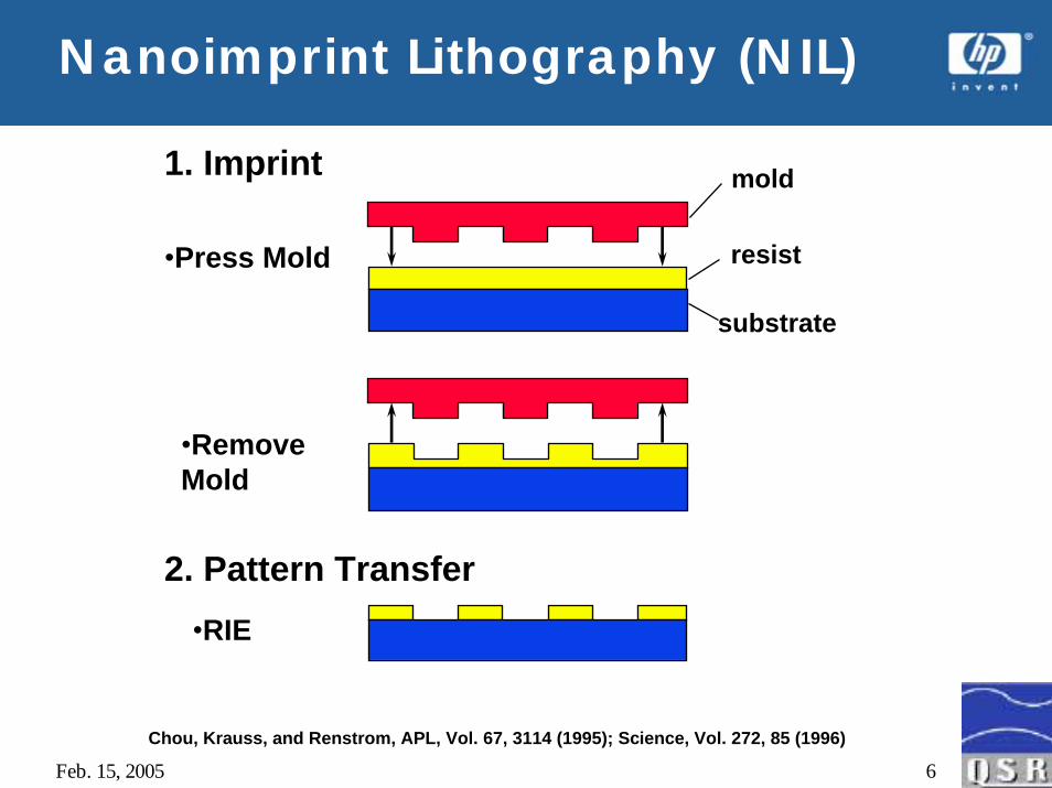
Nanoimprint Lithography (NIL)
1. Imprint mold
resist
substrate
•Press Mold
•Remove Mold
2. Pattern Transfer•RIE
Chou, Krauss, and Renstrom, APL, Vol. 67, 3114 (1995); Science, Vol. 272, 85 (1996)

Feb. 15, 2005 7
Nanoimprint Lithography (NIL)
10 nm
•High resolution-not limited by wavelength
•High throughput -parallel process
•Low cost
Chou, Krauss, and Renstrom, APL, Vol. 67, 3114 (1995); Science, Vol. 272, 85 (1996)

Feb. 15, 2005 8
Step & Flash Imprint
•UV curable process
•Room temperature
•Low pressure
•UV polymer is applied by droping
M. Colburn, A. Grot, G. Wilson’s et al SPIE 2000
Feb. 15, 2005 9
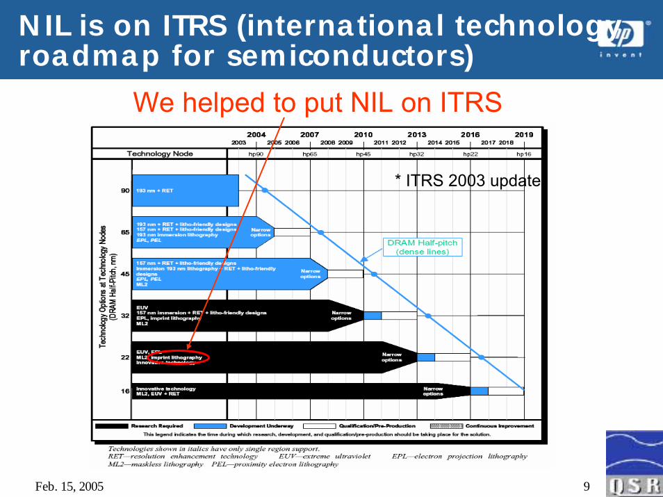
NIL is on ITRS (international technology roadmap for semiconductors)
* ITRS 2003 update
We helped to put NIL on ITRS

Feb. 15, 2005 10
Major Players
Princeton University ---- Nanonex
University of Taxes at Austin ---- Molecular Imprints
University of Michigan
Hewlett-Packard
Motorola
Micro resist…
Europe:
Aachen University. Lund University…
Obducat, EVG, SUSS…
Japan:
Hitachi…
Hewlett-Packard

Crossbar Molecular
Electronics by NIL

Feb. 15, 2005 12
Shrink by 108
Improve power efficiency by 108
ENIAC - circa 1947
HP Pocket PC
What is Next?

Feb. 15, 2005 13
An Architecture for Molecular MolectronicsHPL TeraMAC1 THz multi-architecture
computer• 106 gates operating
at 106 cycle/sec• Built from programmable gate
arrays (FPGA’s)• Computes with look-up tables• Largest defect-tolerant
computer• 220,000 (3%) defective
components
circa 1995Heath, Kuekes, Snider, Williams, Science 280, 1715 (1998)

Feb. 15, 2005 14
An Architecture for Molecular Electronics
A microprocessor (intel P4) A reconfigurable device (FPGA)

Feb. 15, 2005 15
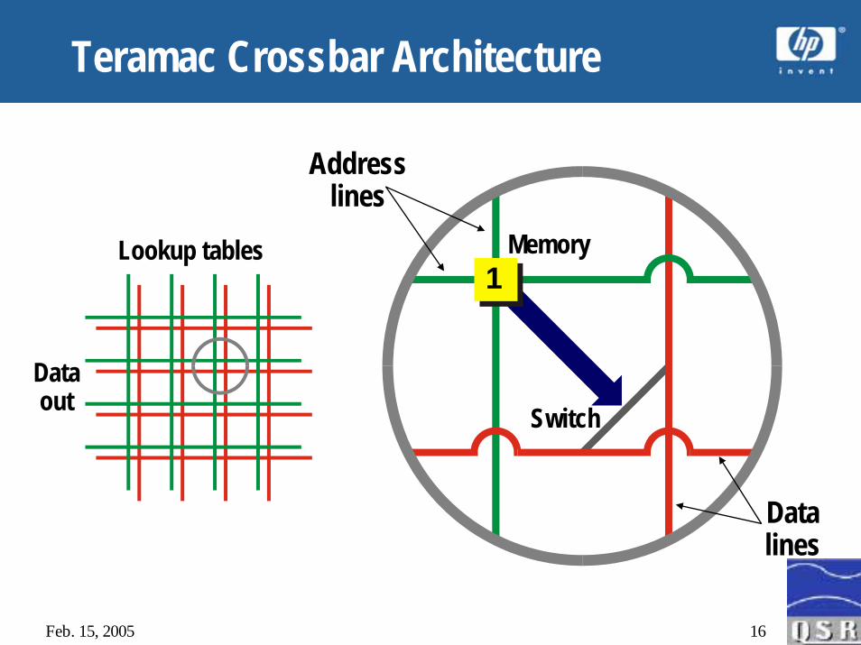
Teramac Crossbar Architecture
Memory
Addresslines
0
Switch
Datalines
Lookup tables
Dataout
Feb. 15, 2005 16
Teramac Crossbar Architecture
Memory
Switch
Datalines
Addresslines
1Lookup tables
Dataout

Feb. 15, 2005 17
Nano-circuit Crossbar Architecture
Molecule
Electrodes
Memory0
Switch
Teramac crossbarY. Chen, G.Y. Jung et al., Nanotech. 14, 462 (2003)

Feb. 15, 2005 18
Crossbar Fabrication: Bottom Electrode
Nanoimprint

Feb. 15, 2005 19
Crossbar Fabrication: Molecule Deposition
Langmuir-Blodgett
Stearic acid
COHO
H3CC18H36O2
26 Å

Feb. 15, 2005 20
Crossbar Fabrication: Top Electrode
Nanoimprint

Feb. 15, 2005 21
Crossbar Fabrication: Etch Back

Feb. 15, 2005 22
1A-H
100
80
60
40
R (1
09oh
m)
20
10
0.8
0.6
0.4
0.2
0
2A-H 3A-H 4A-H 5A-H 6A-H 7A-H 8A-H
H P i n v e n t
Y. Chen, G.Y. Jung et al., Nanotech. 14, 462 (2003)
64 bits Cross-bar Memory at 60 nm Half-pitch by Thermal Nanoimprint Lithography
•First working circuit fabricated using NIL
•First working Molecular memory circuit

Feb. 15, 2005 23
34X34 Cross-bar Structure at 50 nm Half-pitch by UV-curable NIL with Dropping Resist
G.Y. Jung, S. Ganapathiappan et al. Nano Letter 4 (2004),

Feb. 15, 2005 24
Next Goal: 1Kb @ 30nm Half-pitch
Challenges:
•Resist stick to the mold
Mechanical properties and lift-off properties have to be comprimised
•“Rabbit ears” problem

Feb. 15, 2005 25
“Rabbit ears” Problem
Metal Deposition
Undesirable metal “rabbit ears”

Feb. 15, 2005 26
UV-curable NIL with Double-layer Spin-on Resist
1. Prepare substrate, spin under layer and resist (Nanonex NXR 2010) on
4. Mold and substrate separation
5. Residue layer and under layer etching
2. Alignment
UV
6. Metal evaporation and lift-off
3. Press and exposure
W. Wu, H. Ge, S.Y. Chou et al., EIPBN 2004

Feb. 15, 2005 27
Imprinted 30 nm Half-pitch Nanowires on NIL Resist
W. Wu, G-Y Jung, SY Wang, R. S. Williams et al., Applied Physics A in press

Feb. 15, 2005 28
Imprinted 30 nm Half-pitch Nanowires Etched into Under-layer
W. Wu, G-Y Jung, SY Wang, R. S. Williams et al., Applied Physics A in press

Feb. 15, 2005 29
Ti/Pt Nanowires at 30 nm Half-pitch Fabricated Using NIL and Lift-off
W. Wu, G-Y Jung, SY Wang, R. S. Williams et al., Applied Physics A in press

Feb. 15, 2005 30
Rabbit Ears” Solved with Controlled Under-cut
Under layer
ResistMetal
W. Wu, G-Y Jung, SY Wang, R. S. Williams et al., Applied Physics A in press

Feb. 15, 2005 31
30 nm Half-pitch 34X34 Crossbar Molecular Memory Fabricated using NIL and Lift-off
W. Wu, G-Y Jung, SY Wang, R. S. Williams et al., Applied Physics A in press

Feb. 15, 2005 32
30 nm Half-pitch 34X34 Crossbar Molecular Memory Fabricated using NIL and Lift-off
W. Wu, G-Y Jung, SY Wang, R. S. Williams et al., Applied Physics A in press

Feb. 15, 2005 33
30 nm Half-pitch 34X34 Crossbar Molecular Memory Fabricated using NIL and Lift-off
W. Wu, G-Y Jung, SY Wang, R. S. Williams et al., Applied Physics A in press

Feb. 15, 2005 34
30 nm Half-pitch 34X34 Crossbar Molecular Memory Fabricated using NIL and Lift-off
W. Wu, G-Y Jung, SY Wang, R. S. Williams et al., Applied Physics A in press

Feb. 15, 2005 35
30 nm Half-pitch 34X34 Crossbar Molecular Memory Fabricated using NIL and Lift-off
60 nm
W. Wu, G-Y Jung, SY Wang, R. S. Williams et al., Applied Physics A in press

Feb. 15, 2005 36
1X17 Testing Devices Array
40 nm
W. Wu, G-Y Jung, SY Wang, R. S. Williams et al., Applied Physics A in press

Feb. 15, 2005 37
I-V Curve of Single Device

Feb. 15, 2005 38
0V0V
Array Characterization Setup
0V
Vread
0V
Read

Feb. 15, 2005 39
0V0V
Array Characterization Setup
Vprogram or Iprogram
Vprogram/2
Vprogram/2
Program
Write with current
Erase with voltage

Feb. 15, 2005 40
1 2 3 45
67
89
1011
1213
1415
1617
Nat
ive
Writ
ten
2uA
Writ
ten
3uA
Writ
ten
5uA
Era
sed
1.5V
Writ
ten
5uA
0.0E+00
2.0E-08
4.0E-08
6.0E-08
8.0E-08
1.0E-07
1.2E-07
1.4E-07
1.6E-07
Read Current [A]
x Location
State
1x17 Array Read Current at 0.5V
NativeWritten 2uAWritten 3uAWritten 5uAErased 1.5VWritten 5uA
• 15 out of 17 electrodes good• 13/15 devices switch (> 10)• 1 minimal (~3x) • All 15 can be erased• 0 short
Read, Write and Erase of 1X17 Array
W. Wu, G-Y Jung, SY Wang, R. S. Williams et al., Applied Physics A in press

Feb. 15, 2005 41
Programming
Initial state of a subarray After writing into whole subarray
c6c7 c8
r4
r5r6
-4.00E-10
-3.50E-10
-3.00E-10
-2.50E-10
-2.00E-10
-1.50E-10
-1.00E-10
-5.00E-11
0.00E+00
Read
cur
rent
[A]
Subarray Initial State
r4r5r6
c6 c7c8
r4r5
r6
0.E+00
1.E-10
2.E-10
3.E-10
4.E-10
5.E-10
6.E-10
7.E-10
8.E-10
Read
cur
rent
[A]
After 2uA write into whole subarray
r4r5r6

Feb. 15, 2005 42
Crosspoint diode logic array: half-adderDEMUX
U V W X Y Z
A
B
C
D
E
F
DEMU
X
Y = (U AND V) OR (W AND X)Z = V+ C = V-

Nanowire Biological
Sensor

Feb. 15, 2005 44
Sensor chip structure
Zhiyong Li, Yong Chen, Xuema Li,Ted Kamins, and Stan Williams
Nano Letters, 4(2004), 245

Feb. 15, 2005 45
Covalent attachment of ss-DNA on SiNW
OH OH OH
SiMeO
OMeOMe
HS
CCT AAT AAC AATOPO
O
O-
NH
O
O O O
Si
HS
O OSi
HS
Si
HS
O O OO
HS
OSi
HS
Si
TAA
CA
A TA
A TC
C
O
P
O
O O -
N HO
S i
S
1.5nm
Zhiyong Li, Yong Chen, Xuema Li, Ted Kamins, and Stan Williams Nano Letters, 4(2004), 245

Feb. 15, 2005 46
DNA sensing
25 pM
n-SiNW
p-SiNW
Control
TA
CA
AA
TAA
T
CC
SiNWI
nc-ss-DNAA
G
CT
TT
A
A
T
GG
C
TA
CA
AA
TAA
T
CC
SiNWI
TA
CA
AA
TAA
T
CC
p-SiNW
TA
CA
AA
TAA
T
CC
A
G
TT
TT
A
ATT
GG
------
A
G
TT
TT
A
ATT
GG
c-ss-DNA
I ITA
CA
AA
TAA
T
CC
n-SiNW
TA
CA
AA
TAA
T
CC
A
G
TT
TT
A
ATT
GG
------
II
A
G
TT
TT
A
ATT
GG
c-ss-DNA
Zhiyong Li, Yong Chen, Xuema Li, Ted Kamins, and Stan Williams Nano Letters, 4(2004), 245
Feb. 15, 2005 47
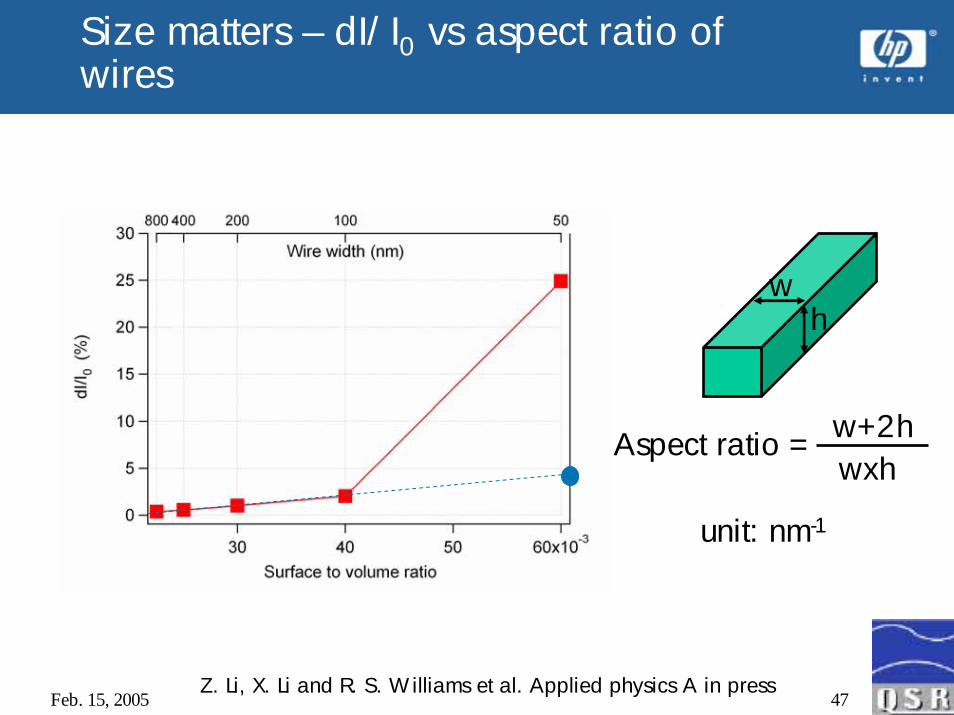
Size matters – dI/I0 vs aspect ratio of wires
wh
w+2hAspect ratio =
unit: nm-1
wxh
Z. Li, X. Li and R. S. Williams et al. Applied physics A in press

Feb. 15, 2005 48
Future Work: Next Generation Nanoimprint Machine
Challenges of NIL:
•Yield (It will be improved over time.)
•Alignment accuracy is currently 10x worse than resolution
-Alignment must be achieved without high cost
Answer:
Next generation nanoimprint machine
•Alignment accuracy is currently 10x worse than resolution
-Alignment must be achieved without high cost

Feb. 15, 2005 49
Nano Displacement Sensing & Estimation (NDSE) Technology (HTL/ Precision Imaging Program)(HTL/ Precision Imaging Program)
•Used in HP large format printers
•Total cost of optics: $60
•1/50 pixel size displacement detectionJ. Gao, C. Picciotto, E. Hoarau, W. Jackson and W. Wu NNT 2004 and Applied physics A in press

Feb. 15, 2005 50
5 nm Displacement sensing using NDSE
J. Gao, C. Picciotto, E. Hoarau, W. Jackson and W. Wu NNT 2004 and Applied physics A in press

Feb. 15, 2005 51
Next Generation Nanoimprint Machine
Nanoimprint

Feb. 15, 2005 52
Summary
• HP is one of the earliest company/university to investigate NIL.
• QSR of HP labs is the first group made working circuit using NIL.
• Crossbar molecular memory with record density of 28 Gb/cm2 (30 nm half pitch) were fabricated using NIL.
• NIL is capable of making real applications.
• Three generations of nanoimprinters were built by QSR.
• Fast and low-cost mold duplication process was developed to lower the cost of NIL further.
• Next generation nanoimprinter will integrate NIL and HP’s precision imaging technology.

Feb. 15, 2005 53
Acknowledgement
• My colleagues and collaborators • Supported in part by DARPA• IEEE SF Bay Area Nanotechnology Council• You

Feb. 15, 2005 54