Embed Size (px)
Citation preview

Semiconductor Production Equipment Group, Canon Inc.
Progress of Nanoimprint System
Development for High Volume
Manufacturing of Semiconductor Devices
Hideyuki WadaSemiconductor Production Equipment Group
Canon Inc.
October 27th, 2016

Semiconductor Production Equipment Group, Canon Inc. 2/28
Introduction
Nanoimprint Technology Overview
System Roadmap and Cost of Ownership
Nanoimprint System Performance Update
• Overlay
• Throughput
• Defectivity & Particle Control
Mask Replication System
• Image Placement Improvement
• Preliminary Test Results
Conclusions
Outline

Semiconductor Production Equipment Group, Canon Inc. 3/28
Jet and Flash Imprint Lithography* (J-FIL*)has been developed for the past decade to meet the requirements for
semiconductor manufacturing.
The technology is now readyfor the fabrication of memory devices at 20nm and below. Moreover,
Canon’s Nanoimprint Lithography systems have been used to make
working 1Xnm devices since 2014.
Imprint lithography offers many advantagesin terms of cost of ownership (CoO) in addition to its excellent resolution.
This presentation will focus on the following key CoO drivers:
• Process cost: SAQP less Direct Imprinting
• Critical litho cost: High yield and High throughput by Nanoimprint Systems
• Mask cost: New Mask Replication Systems (FPA-1100 NR2)
Introduction
* Jet and Flash Imprint Lithography and J-FIL are trademarks of Molecular Imprints, Inc.

Semiconductor Production Equipment Group, Canon Inc. 4/28
Nanoimprint Technology
Overview

Semiconductor Production Equipment Group, Canon Inc. 5/28
Introduction of Nanoimprint Technology

Semiconductor Production Equipment Group, Canon Inc. 6/28
Mean StdDev Stdev/mean
Dot diameter [nm] 16.6 1.1 5.6%
Dot area [nm2] 216.2 21.4 9.8%
RLT [nm] ~8nm
Figure 1. NuTera HD7000 disk imprinting
tool
Figure 3. a) 1Tb/in2 bit pattern with a pitch of 27nm. The average dot diameter was measured
using Simagis software and was 16.6nm with a 1s deviation of 1.1nm.
Figure 2. Schematic representation of a J-
FIL disk imprint process.
Figure 4. Reduced pattern collapse (b) as a result of using a resist with a higher modulus.
Resolution Capability
2D Patterning
10nm Pillars14nm Holes25nm Holes
28nm 16nm 11nm
22nm
High resolution, low line edge roughness, greater design freedom
Line and Space
Holes and Pillars

Semiconductor Production Equipment Group, Canon Inc. 7/28
Choice of <2xnm CH Lithography
• SAQP=Self Aligned Quadruple Patterning
Good CDU
By no shot noise
Single Patterning
- improves process cost
- reduces cycle time
Poor CDU
By shot noise
Low throughput
By low resist sensitivity
EUVL
ArF IML (Multi Patterning)
J-FIL
SAQP
SAQP
2x SAQP brings
- cost impact
- severe OL requirement
Canon offers improved performance for device manufacturing

Semiconductor Production Equipment Group, Canon Inc. 8/28
RoadmapSystem Roadmap and
Cost of Ownership
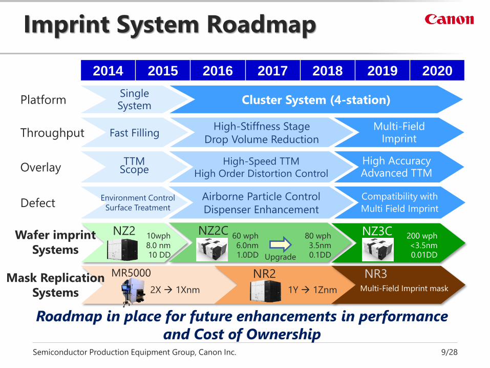
Semiconductor Production Equipment Group, Canon Inc. 9/28
MR5000
Roadmap in place for future enhancements in performance
and Cost of Ownership
2014 2015 2016 2017 2018 2019 2020
Platform
Throughput
Overlay
Defect
High-Stiffness Stage
Drop Volume Reduction
Multi-Field Imprint
Fast Filling
Single System
Cluster System (4-station)
TTM Scope
High-Speed TTM
High Order Distortion Control
Airborne Particle Control
Dispenser Enhancement
Compatibility with
Multi Field Imprint
NZ2 10wph8.0 nm10 DD
NZ2C NZ3C 200 wph<3.5nm0.01DD
Wafer imprint
Systems
Environment Control
Surface Treatment
High AccuracyAdvanced TTM
80 wph3.5nm0.1DDUpgrade
60 wph6.0nm1.0DD
Imprint System Roadmap
2X 1Xnm
NR2 NR3Multi-Field Imprint mask
Mask Replication
Systems 1Y 1Znm

Semiconductor Production Equipment Group, Canon Inc. 10/28
105.1
72.6
55.7
40.5
0
20
40
60
80
100
120
(ArF IML+SADP) x 2 ArF IML +SAQP EUVL NZ2C
Critical Litho Cost Mask Cost Other Process CostEstimated by Canon
TP=250wph TP=250wph TP=125wph TP=60wph
61% Reduction
44% Reduction
Co
st p
er
Wafe
r Level ($
)
Contact Holes
Line & Space
Comparison of CoO ArF IML, EUV and J-FIL (NZ2C System)
J-FIL technology provides the lowest CoO

Semiconductor Production Equipment Group, Canon Inc. 11/28
Nanoimprint System
Technology

Semiconductor Production Equipment Group, Canon Inc. 12/28
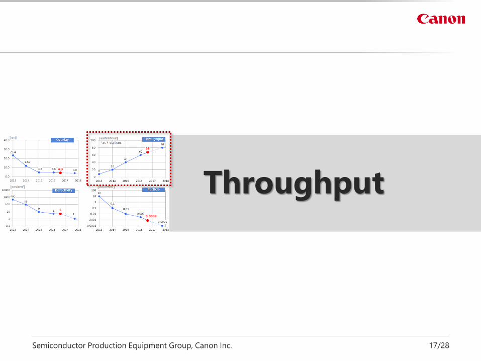
480
96
95 5
1
0.1
1
10
100
1000
10000
2013 2014 2015 2016 2017 2018
23.4
12.0
4.8 4.8 4.3 4.0
0.0
10.0
20.0
30.0
40.0
2013 2014 2015 2016 2017 2018
Evolution of system performance
8
20
40
60 68
80
0
20
40
60
80
100
2013 2014 2015 2016 2017 2018
10
0.1
0.01
0.0030.0008
0.0001
0.0001
0.001
0.01
0.1
1
10
100
2013 2014 2015 2016 2017 2018
[nm]
[pcs/wafer]
[wafer/hour]
[pcs/cm2]
*as 4 stationsOverlay
Defectivity Particle
Throughput
• Canon has made great progress on system performance
• Throughput and yield improvements reduce “Critical litho cost” of CoO

Semiconductor Production Equipment Group, Canon Inc. 13/28
Overlay

Semiconductor Production Equipment Group, Canon Inc. 14/28
Overlay Performance
X Y
Average -0.1 nm 0.0 nm
3σ 4.1 nm 4.2 nm
Ave.+3σ 4.2 nm 4.3 nm
Tool : FPA-1200 NZ2C
Mask : Test mask
with 2x nm features
Substrate : ArF IML
No. of fields : 84 (full and partial)
No. of measured points : 12 / field
Mix-and-match overlay of 4.3nm was achieved

Semiconductor Production Equipment Group, Canon Inc. 15/28
High Order Distortion Control
Nanoimprint Lithography
UV light
Mask
Wafer
Stage
Digital Micro mirror device
Mirror size : □10μmNumbers: 1024×768pcs.
Laser(465nm)
WaferMask
Compensation Field
Mirror
High Order Distortion Control

Semiconductor Production Equipment Group, Canon Inc. 16/28
Results of HODC
W/m2
K
mm
mm
No correction Mag. Actuator Mag. Actuator+ HODC
128 nm 2.35 nm 0.67nm
Mask
Wafer
High Order Distortion Control will soon be implemented
-10
-5
0
5
10
15
20
-10 -5 0 5 10 15 20
Exp
._Y
[nm
]
Sim._Y [nm]
3σ :1.2nm
Simulation
Exp
eri
men
t
HODC Test Result
[nm]
[nm
]
Heat Input [W/m2] Wafer Temperature ΔT[K] Shot Distortion(3σ)
Semiconductor Production Equipment Group, Canon Inc. 17/28
Throughput

Semiconductor Production Equipment Group, Canon Inc. 18/28
2012 2013 2014 2016
Throughput
[wph] (4-Station)6 20 40 68
Throughput / Station 1.5 5.0 10.0 17.0
Overhead 900 sec 168 sec 38 sec 17 sec
Imprint time 1,500 sec 552 sec 322 sec 195 sec
Filling 1,260 sec 434 sec 214 sec 101 sec
Process Time /
Wafer
Throughput Improvement History
Reduction of filling time is the key for high TP
Overhead Time
Imprint Time
(dispense, filling, exposure,
separation and others)
21
2 s
ec
36
0 s
ec
72
0 s
ec2,4
00
sec
60% 48%

Semiconductor Production Equipment Group, Canon Inc. 19/28
Reduction of Filling Time
Key factors to filling time are:
• System controls (to avoid gas trapping)
• Pattern layout (design for imprint)
• Drop volume (smaller is better)
• Accelerating drop spread time (Material improvement)
0,6
0,7
0,8
0,9
1
1,1
1,2
1,3
1,4
1,5
1,6
0 50 100 150 200 250
Filli
ng
Tim
e (
sec)
Drop Diameter (µm)
FT385M, 1pL
FT385M2, 1pL
FTxxx, 1pL
Hp28nm L/S
Resist
Substrate
Mask
Conventional Material New Material
Fast filling
Filling time of new material is 40% shorter than the conventional one
Drop Spread Diameter (um)

Semiconductor Production Equipment Group, Canon Inc. 20/28
Defectivity & Particle

Semiconductor Production Equipment Group, Canon Inc. 21/28
Defectivity: Major Defect Mechanisms
Liquid phase
Incomplete fluid filling : Non-fill defect
Nanoscale voids caused by surface
contamination
Solid phase
Separation mechanics : Plug defect
Line breaks caused by resist particle
contamination
Fall-on Particles
Plug Defect Line Break
Nanoscale VoidNon-fill Defect
Fall-on Particle Mask Damage
• Material Improvements
• Appropriate Environment Control
• Imprint – Separation Mechanics
Optimization
• Particle Elimination in Resist
• Adder Particle Reduction by Air Flow
Optimization
Semiconductor Production Equipment Group, Canon Inc. 22/28
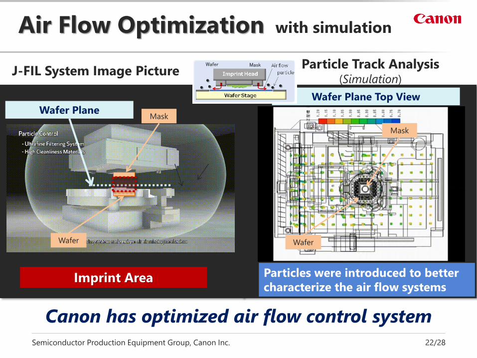
Air Flow Optimization with simulation
Imprint Area
Canon has optimized air flow control system
J-FIL System Image Picture
Wafer PlaneMask
Wafer
Particle Track Analysis(Simulation)
Particles were introduced to better
characterize the air flow systems
Wafer Plane Top View
Mask
Wafer
MaskWafer

Semiconductor Production Equipment Group, Canon Inc. 23/28
10
0,1
0,01
0.00080,0001
0,001
0,01
0,1
1
10
100
2013 2014 2015 2016 2017 2018
Next Generation
Air curtain system
Entire Air flow control
Primary
Air curtain system
Surface treatment
New automatic wafer
cleaning system
Ionizer
Ionizer
Optimization
Canon has demonstrated a particle adder over 1,000 wafer run
0.001
[pcs/wafer]
Equivalent to
1000 wafers0.003
Particle Adder History and Roadmap
Semiconductor Production Equipment Group, Canon Inc. 24/28
m Mask Replication System

Semiconductor Production Equipment Group, Canon Inc. 25/28
“Mask Replication System” is necessary to provide low cost replica masks;
therefore, Canon is developing new mask replication system (NR2).
To provide low cost and fine pattern replica masks, the following
technologies are necessary for NR2:
• Particle reduction to extend the lifetime of a master mask
• Image placement improvement to transfer fine patterns of the master mask
to replica masks for direct imprinting
New Mask Replication System
Master Mask
(Very High Cost Mask)
Replica Mask
(Low Cost Mask)
Mask Replication
System (FPA-1100NR2)
NR2 will be installed at a customer site in 4th Quarter

Semiconductor Production Equipment Group, Canon Inc. 26/28
Target IP adder is 1nm
Mask chuck and substrate flatness, along with imprint separation and
motion control will drive the IP performance improvement
Image Placement Accuracy
Semiconductor Production Equipment Group, Canon Inc. 27/28
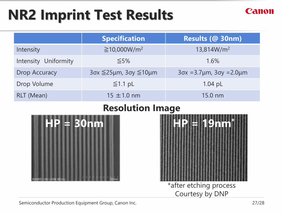
NR2 Imprint Test Results
Specification Results (@ 30nm)
Intensity ≧10,000W/m2 13,814W/m2
Intensity Uniformity ≦5% 1.6%
Drop Accuracy 3σx ≦25μm, 3σy ≦10μm 3σx =3.7μm, 3σy =2.0μm
Drop Volume ≦1.1 pL 1.04 pL
RLT (Mean) 15 ±1.0 nm 15.0 nm
Resolution Image
HP = 30nm
*after etching process
Courtesy by DNP
HP = 19nm*

Semiconductor Production Equipment Group, Canon Inc. 28/28
The performance of J-FIL system is ready for both L/S & CH of
1Xnm mass production trial
Both Wafer Imprint and Mask Replication systems are available
Very competitive CoO is realized by Direct Imprint technology
that can reduce process cost relative to multiple patterning
technology
Conclusions
Canon is strongly committed to lead
Nanoimprint technology development for
semiconductor device high volume
manufacturing