Embed Size (px)
Citation preview
2.7 V to 5.5 V, 450 μA, Rail-to-Rail Output, Quad, 12-/16-Bit nanoDACs
Data Sheet AD5624/AD5664
Rev. A Document Feedback Information furnished by Analog Devices is believed to be accurate and reliable. However, no responsibility is assumed by Analog Devices for its use, nor for any infringements of patents or other rights of third parties that may result from its use. Specifications subject to change without notice. No license is granted by implication or otherwise under any patent or patent rights of Analog Devices. Trademarks and registered trademarks are the property of their respective owners.
One Technology Way, P.O. Box 9106, Norwood, MA 02062-9106, U.S.A.Tel: 781.329.4700 ©2006–2018 Analog Devices, Inc. All rights reserved. Technical Support www.analog.com
FEATURES Low power, quad nanoDACs
AD5664: 16 bits AD5624: 12 bits
Relative accuracy: ±12 LSBs max Guaranteed monotonic by design 10-lead MSOP and 3 mm × 3 mm LFCSP_WD 2.7 V to 5.5 V power supply Power-on reset to zero Per channel power-down Serial interface, up to 50 MHz
APPLICATIONS Process control Data acquisition systems Portable battery-powered instruments Digital gain and offset adjustment Programmable voltage and current sources Programmable attenuators
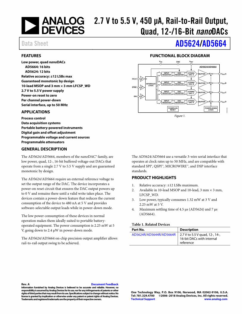
FUNCTIONAL BLOCK DIAGRAM
INTERFACELOGIC
SCLK
SYNC
DIN
INPUTREGISTER
DACREGISTER
VDD GND
POWER-ONRESET
STRINGDAC A BUFFER
VREF
VOUTA
INPUTREGISTER
DACREGISTER
STRINGDAC B BUFFER VOUTB
INPUTREGISTER
DACREGISTER
STRINGDAC C BUFFER VOUTC
INPUTREGISTER
DACREGISTER
STRINGDAC D BUFFER VOUTD
AD5624/AD5664
POWER-DOWNLOGIC
0594
3-00
1
Figure 1.
GENERAL DESCRIPTION
The AD5624/AD5664, members of the nanoDAC® family, are low power, quad, 12-, 16-bit buffered voltage-out DACs that operate from a single 2.7 V to 5.5 V supply and are guaranteed monotonic by design.
The AD5624/AD5664 require an external reference voltage to set the output range of the DAC. The device incorporates a power-on reset circuit that ensures the DAC output powers up to 0 V and remains there until a valid write takes place. The devices contain a power-down feature that reduces the current consumption of the device to 480 nA at 5 V and provides software-selectable output loads while in power-down mode.
The low power consumption of these devices in normal operation makes them ideally suited to portable battery-operated equipment. The power consumption is 2.25 mW at 5 V, going down to 2.4 μW in power-down mode.
The AD5624/AD5664 on-chip precision output amplifier allows rail-to-rail output swing to be achieved.
The AD5624/AD5664 use a versatile 3-wire serial interface that operates at clock rates up to 50 MHz, and are compatible with standard SPI®, QSPI™, MICROWIRE™, and DSP interface standards.
PRODUCT HIGHLIGHTS
1. Relative accuracy: ±12 LSBs maximum.2. Available in 10-lead MSOP and 10-lead, 3 mm × 3 mm,
LFCSP_WD.3. Low power, typically consumes 1.32 mW at 3 V and
2.25 mW at 5 V.4. Maximum settling time of 4.5 μs (AD5624) and 7 μs
(AD5664).
Table 1. Related Devices Part No. Description AD5624R/AD5644R/AD5664R 2.7 V to 5.5 V quad, 12-, 14-,
16-bit DACs with internal reference
AD5624/AD5664 Data Sheet
Rev. A | Page 2 of 23
TABLE OF CONTENTS Features .............................................................................................. 1
Applications ....................................................................................... 1
Functional Block Diagram .............................................................. 1
General Description ......................................................................... 1
Product Highlights ........................................................................... 1
Revision History ............................................................................... 2
Specifications ..................................................................................... 3
AC Characteristics ........................................................................ 4
Timing Characteristics ................................................................ 5
Timing Diagram ........................................................................... 5
Absolute Maximum Ratings ............................................................ 6
ESD Caution .................................................................................. 6
Pin Configuration and Function Descriptions ............................. 7
Typical Performance Characteristics ............................................. 8
Terminology .................................................................................... 13
Theory of Operation ...................................................................... 15
D/A Section ................................................................................. 15
Resistor String ............................................................................. 15
Output Amplifier ........................................................................ 15
Serial Interface ............................................................................ 15
Input Shift Register .................................................................... 16
SYNC Interrupt .......................................................................... 16
Power-On Reset .......................................................................... 16
Software Reset ............................................................................. 17
Power-Down Modes .................................................................. 17
LDAC Function .......................................................................... 18
Microprocessor Interfacing ....................................................... 19
Applications Information .............................................................. 20
Choosing a Reference for the AD5624/AD5664 ........................ 20
Using a Reference as a Power Supply for the AD5624/AD5664 ........................................................................ 20
Bipolar Operation Using the AD5624/AD5664 ......................... 21
Using AD5624/AD5664 with a Galvanically Isolated Interface ....................................................................................... 21
Power Supply Bypassing and Grounding ................................ 21
Outline Dimensions ....................................................................... 22
Ordering Guide ............................................................................... 23
REVISION HISTORY
6/2018—Rev. 0 to Rev. A Changes to Figure 3 Caption and Table 6 ...................................... 7 Add Figure 4; Renumber Sequentially ........................................... 7 Changed Applications Section to Applications Information Section .............................................................................................. 20 Updated Outline Dimensions ....................................................... 22 Changes to Ordering Guide .......................................................... 23
6/2006—Revision 0: Initial Version
Data Sheet AD5624/AD5664
Rev. A | Page 3 of 23
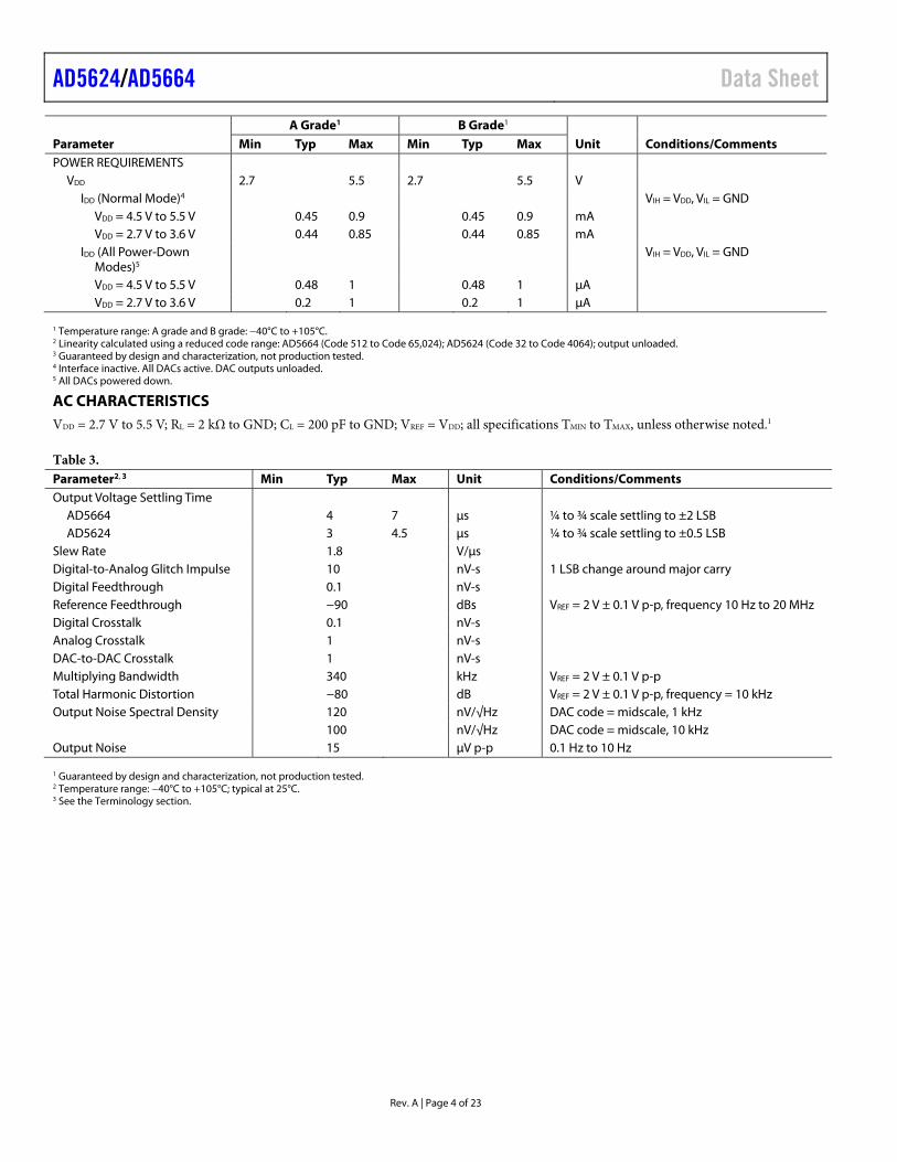
SPECIFICATIONS VDD = +2.7 V to +5.5 V; RL = 2 kΩ to GND; CL = 200 pF to GND; VREF = VDD; all specifications TMIN to TMAX, unless otherwise noted.
Table 2. A Grade1 B Grade1
Parameter Min Typ Max Min Typ Max Unit Conditions/Comments STATIC PERFORMANCE2
AD5664Resolution 16 16 BitsRelative Accuracy ±8 ±16 ±6 ±12 LSB Differential Nonlinearity ±1 ±1 LSB Guaranteed monotonic by
design AD5624
Resolution 12 BitsRelative Accuracy ±0.5 ±1 LSB Differential Nonlinearity ±0.25 LSB Guaranteed monotonic by
design Zero Code Error 2 10 2 10 mV All zeroes loaded to DAC register Offset Error ±1 ±10 ±1 ±10 mV Full-Scale Error −0.1 ±1 −0.1 ±1 % of FSR All ones loaded to DAC register Gain Error ±1.5 ±1.5 % of FSR Zero Code Error Drift ±2 ±2 μV/°C Gain Temperature
Coefficient ±2.5 ±2.5 ppm Of FSR/°C
DC Power Supply Rejection Ratio
−100 −100 dB DAC code = midscale ; VDD ± 10%
DC Crosstalk 10 10 μV Due to full-scale output change RL = 2 kΩ to GND or VDD
10 10 μV/mA Due to load current change 5 5 μV Due to powering down (per
channel) OUTPUT CHARACTERISTICS3
Output Voltage Range 0 VDD 0 VDD V Capacitive Load Stability 2 2 nF RL = ∞
10 10 nF RL = 2 kΩ DC Output Impedance 0.5 0.5 Ω Short-Circuit Current 30 30 mA VDD = 5 V Power-Up Time 4 4 μs Coming out of power-down
mode; VDD = 5 V REFERENCE INPUTS
Reference Current 170 200 170 200 μA VREF = VDD = 5.5 V Reference Input Range 0.75 VDD 0.75 VDD V Reference Input Impedance 26 26 kΩ
LOGIC INPUTS3
Input Current ±2 ±2 μA All digital inputs VINL, Input Low Voltage 0.8 0.8 V VDD = 5 V, 3 V VINH, Input High Voltage 2 2 V VDD = 5 V, 3 V Pin Capacitance 3 3 pF
AD5624/AD5664 Data Sheet
Rev. A | Page 4 of 23
A Grade1 B Grade1
Parameter Min Typ Max Min Typ Max Unit Conditions/Comments POWER REQUIREMENTS
VDD 2.7 5.5 2.7 5.5 VIDD (Normal Mode)4 VIH = VDD, VIL = GND
VDD = 4.5 V to 5.5 V 0.45 0.9 0.45 0.9 mA VDD = 2.7 V to 3.6 V 0.44 0.85 0.44 0.85 mA
IDD (All Power-Down Modes)5
VIH = VDD, VIL = GND
VDD = 4.5 V to 5.5 V 0.48 1 0.48 1 μA VDD = 2.7 V to 3.6 V 0.2 1 0.2 1 μA
1 Temperature range: A grade and B grade: −40°C to +105°C. 2 Linearity calculated using a reduced code range: AD5664 (Code 512 to Code 65,024); AD5624 (Code 32 to Code 4064); output unloaded. 3 Guaranteed by design and characterization, not production tested. 4 Interface inactive. All DACs active. DAC outputs unloaded. 5 All DACs powered down.
AC CHARACTERISTICS VDD = 2.7 V to 5.5 V; RL = 2 kΩ to GND; CL = 200 pF to GND; VREF = VDD; all specifications TMIN to TMAX, unless otherwise noted.1
Table 3. Parameter2, 3 Min Typ Max Unit Conditions/CommentsOutput Voltage Settling Time
AD5664 4 7 μs ¼ to ¾ scale settling to ±2 LSB AD5624 3 4.5 μs ¼ to ¾ scale settling to ±0.5 LSB
Slew Rate 1.8 V/μs Digital-to-Analog Glitch Impulse 10 nV-s 1 LSB change around major carry Digital Feedthrough 0.1 nV-s Reference Feedthrough −90 dBs VREF = 2 V ± 0.1 V p-p, frequency 10 Hz to 20 MHz Digital Crosstalk 0.1 nV-s Analog Crosstalk 1 nV-s DAC-to-DAC Crosstalk 1 nV-s Multiplying Bandwidth 340 kHz VREF = 2 V ± 0.1 V p-p Total Harmonic Distortion −80 dB VREF = 2 V ± 0.1 V p-p, frequency = 10 kHz Output Noise Spectral Density 120 nV/√Hz DAC code = midscale, 1 kHz
100 nV/√Hz DAC code = midscale, 10 kHz Output Noise 15 μV p-p 0.1 Hz to 10 Hz
1 Guaranteed by design and characterization, not production tested. 2 Temperature range: −40°C to +105°C; typical at 25°C. 3 See the Terminology section.
Data Sheet AD5624/AD5664
Rev. A | Page 5 of 23
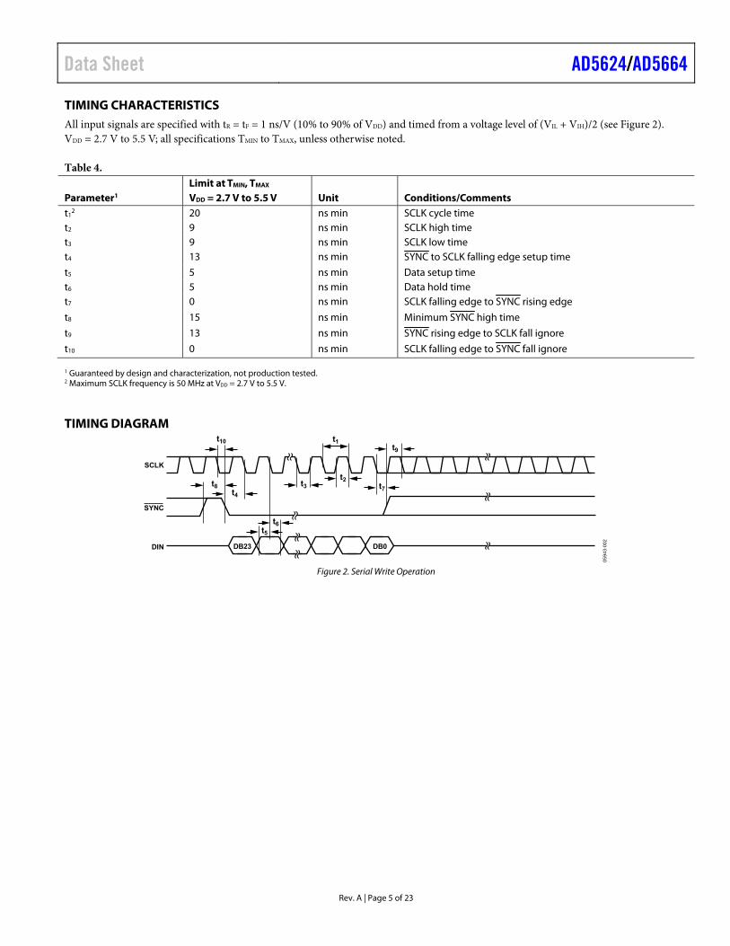
TIMING CHARACTERISTICS All input signals are specified with tR = tF = 1 ns/V (10% to 90% of VDD) and timed from a voltage level of (VIL + VIH)/2 (see Figure 2). VDD = 2.7 V to 5.5 V; all specifications TMIN to TMAX, unless otherwise noted.
Table 4. Limit at TMIN, TMAX
Parameter1 VDD = 2.7 V to 5.5 V Unit Conditions/Comments t1
2 20 ns min SCLK cycle time t2 9 ns min SCLK high time t3 9 ns min SCLK low time t4 13 ns min SYNC to SCLK falling edge setup time
t5 5 ns min Data setup time t6 5 ns min Data hold time t7 0 ns min SCLK falling edge to SYNC rising edge
t8 15 ns min Minimum SYNC high time
t9 13 ns min SYNC rising edge to SCLK fall ignore
t10 0 ns min SCLK falling edge to SYNC fall ignore
1 Guaranteed by design and characterization, not production tested. 2 Maximum SCLK frequency is 50 MHz at VDD = 2.7 V to 5.5 V.
TIMING DIAGRAM
DB0DB23
t10
SCLK
SYNC
DIN
t1t9
t7
t2t3
t6t5
t4
t8
0594
3-00
2
Figure 2. Serial Write Operation
AD5624/AD5664 Data Sheet
Rev. A | Page 6 of 23
ABSOLUTE MAXIMUM RATINGS TA = 25°C, unless otherwise noted.
Table 5. Parameter RatingVDD to GND −0.3 V to +7 V VOUT to GND −0.3 V to VDD + 0.3 V VREF to GND −0.3 V to VDD + 0.3 V Digital Input Voltage to GND −0.3 V to VDD + 0.3 V Operating Temperature Range
Industrial (A Grade, B Grade) −40°C to +105°C Storage Temperature Range −65°C to +150°C Junction Temperature (TJ max) 150°C
Power Dissipation (TJ max − TA)/θJA LFCSP_WD Package (4-Layer Board)
θJA Thermal Impedance 61°C/W MSOP Package (4-Layer Board)
θJA Thermal Impedance 142°C/W θJC Thermal Impedance 43.7°C/W
Reflow Soldering Peak Temperature Pb-Free 260°C ± 5°C
Stresses at or above those listed under Absolute Maximum Ratings may cause permanent damage to the product. This is a stress rating only; functional operation of the product at these or any other conditions above those indicated in the operational section of this specification is not implied. Operation beyond the maximum operating conditions for extended periods may affect product reliability.
ESD CAUTION
Data Sheet AD5624/AD5664
Rev. A | Page 7 of 23
PIN CONFIGURATION AND FUNCTION DESCRIPTIONS
1VOUTA 10 VREF
2VOUTB 9 VDD
3GND 8 DIN
4VOUTC 7 SCLK
5VOUTD 6 SYNC
AD5624/AD5664TOP VIEW
(Not to Scale)
0594
3-00
3
Figure 3. 10-Lead MSOP Pin Configuration
VOUTA VREF
VOUTB VDD
GND DIN
VOUTC SCLK
VOUTD SYNC
0594
3-10
4
1
2
3
4
5
10
NOTES1. EXPOSED PAD TIED TO GND ON LFCSP PACKAGE.
9
8
7
6
AD5624/AD5664TOP VIEW
(Not to Scale)
Figure 4. 10-Lead LFCSP Pin Configuration
Table 6. Pin Function Descriptions Pin No. Mnemonic Description 1 VOUTA Analog Output Voltage from DAC A. The output amplifier has rail-to-rail operation. 2 VOUTB Analog Output Voltage from DAC B. The output amplifier has rail-to-rail operation. 3 GND Ground Reference Point for All Circuitry on the device 4 VOUTC Analog Output Voltage from DAC C. The output amplifier has rail-to-rail operation. 5 VOUTD Analog Output Voltage from DAC D. The output amplifier has rail-to-rail operation. 6 SYNC Active Low Control Input. This is the frame synchronization signal for the input data. When SYNC goes low, it powers on
the SCLK and DIN buffers and enables the input shift register. Data is transferred in on the falling edges of the next 24 clocks. If SYNC is taken high before the 24th falling edge, the rising edge of SYNC acts as an interrupt and the write sequence is ignored by the device.
7 SCLK Serial Clock Input. Data is clocked into the input shift register on the falling edge of the serial clock input. Data can be transferred at rates up to 50 MHz.
8 DIN Serial Data Input. This device has a 24-bit input shift register. Data is clocked into the register on the falling edge of the serial clock input.
9 VDD Power Supply Input. These devices can be operated from 2.7 V to 5.5 V. The supply is decoupled with a 10 μF capacitor in parallel with a 0.1 μF capacitor to GND.
10 VREF Reference Voltage Input. EPAD Exposed Pad. Exposed pad tied to GND on LFCSP package.
AD5624/AD5664 Data Sheet
Rev. A | Page 8 of 23
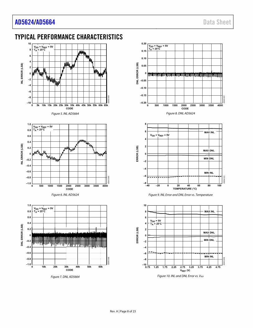
TYPICAL PERFORMANCE CHARACTERISTICS
CODE
INL
ER
RO
R (
LS
B)
10
4
6
8
0
2
–6
–10
–8
–2
–4
0 5k 10k 15k 20k 25k 30k 35k 40k 45k 50k 55k 60k 65k05
943-
004
VDD = VREF = 5VTA = 25°C
Figure 5. INL AD5664
CODE
INL
ER
RO
R (
LS
B)
1.0
–1.00 500 1000 1500 2000 2500 3000 3500 4000
0594
3-00
5
–0.8
–0.6
–0.4
0
0.4
0.2
–0.2
0.6
0.8
VDD = VREF = 5VTA = 25°C
Figure 6. INL AD5624
CODE
DN
L E
RR
OR
(L
SB
)
1.0
0.6
0.4
0.2
0.8
0
–0.4
–0.2
–0.6
–1.0
–0.8
0 10k 20k 30k 40k 50k 60k
0594
3-00
6
VDD = VREF = 5VTA = 25°C
Figure 7. DNL AD5664
DN
L E
RR
OR
(L
SB
)
0.20
0.10
0.05
0.15
0
–0.05
–0.10
–0.20
–0.15
0594
3-00
7
CODE0 500 1000 1500 2000 2500 3000 3500 4000
VDD = VREF = 5VTA = 25°C
Figure 8. DNL AD5624
TEMPERATURE (°C)
ER
RO
R (
LS
B)
8
6
4
2
–6
–4
–2
0
–8–40 –20 40200 1008060
0585
6-02
2
MIN DNL
MAX DNL
MAX INL
MIN INL
VDD = VREF = 5V
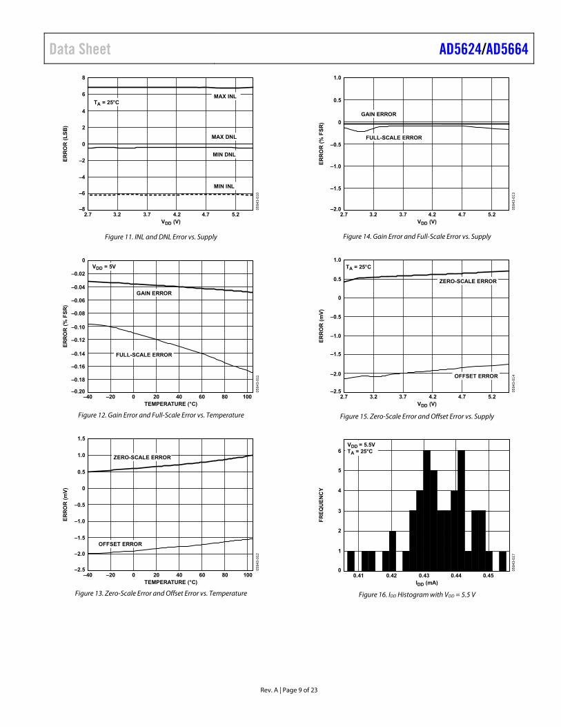
Figure 9. INL Error and DNL Error vs. Temperature
VREF (V)
ER
RO
R (
LS
B)
10
4
6
8
2
0
–8
–6
–4
–2
–100.75 1.25 1.75 2.25 4.253.753.252.75 4.75
0594
3-00
9
MIN DNL
MAX DNL
MAX INL
MIN INL
VDD = 5VTA = 25°C
Figure 10. INL and DNL Error vs. VREF
Data Sheet AD5624/AD5664
Rev. A | Page 9 of 23
VDD (V)
ER
RO
R (
LS
B)
8
6
4
2
–6
–4
–2
0
–82.7 3.2 3.7 4.74.2 5.2
0594
3-01
0
MIN DNL
MAX DNL
MAX INL
MIN INL
TA = 25°C
Figure 11. INL and DNL Error vs. Supply
TEMPERATURE (°C)
ER
RO
R (
% F
SR
)
0
–0.04
–0.02
–0.06
–0.08
–0.10
–0.18
–0.16
–0.14
–0.12
–0.20–40 –20 40200 1008060
0594
3-01
1
VDD = 5V
GAIN ERROR
FULL-SCALE ERROR
Figure 12. Gain Error and Full-Scale Error vs. Temperature
TEMPERATURE (°C)
ER
RO
R (
mV
)
1.5
1.0
0.5
0
–2.0
–1.5
–1.0
–0.5
–2.5–40 –20 40200 8060 100
0594
3-01
2
OFFSET ERROR
ZERO-SCALE ERROR
Figure 13. Zero-Scale Error and Offset Error vs. Temperature
VDD (V)
ER
RO
R (
% F
SR
)
1.0
–1.5
–1.0
–0.5
0
0.5
–2.02.7 3.2 3.7 4.74.2 5.2
0594
3-01
3
GAIN ERROR
FULL-SCALE ERROR
Figure 14. Gain Error and Full-Scale Error vs. Supply
VDD (V)
ER
RO
R (
mV
)
1.0
0.5
0
–2.0
–1.5
–1.0
–0.5
–2.52.7 3.2 4.23.7 5.24.7
0594
3-01
4
ZERO-SCALE ERROR
OFFSET ERROR
TA = 25°C
Figure 15. Zero-Scale Error and Offset Error vs. Supply
IDD (mA)
FR
EQ
UE
NC
Y
0
1
2
3
4
5
6
0.41 0.42 0.43 0.44 0.45
0594
3-01
7
VDD = 5.5VTA = 25°C
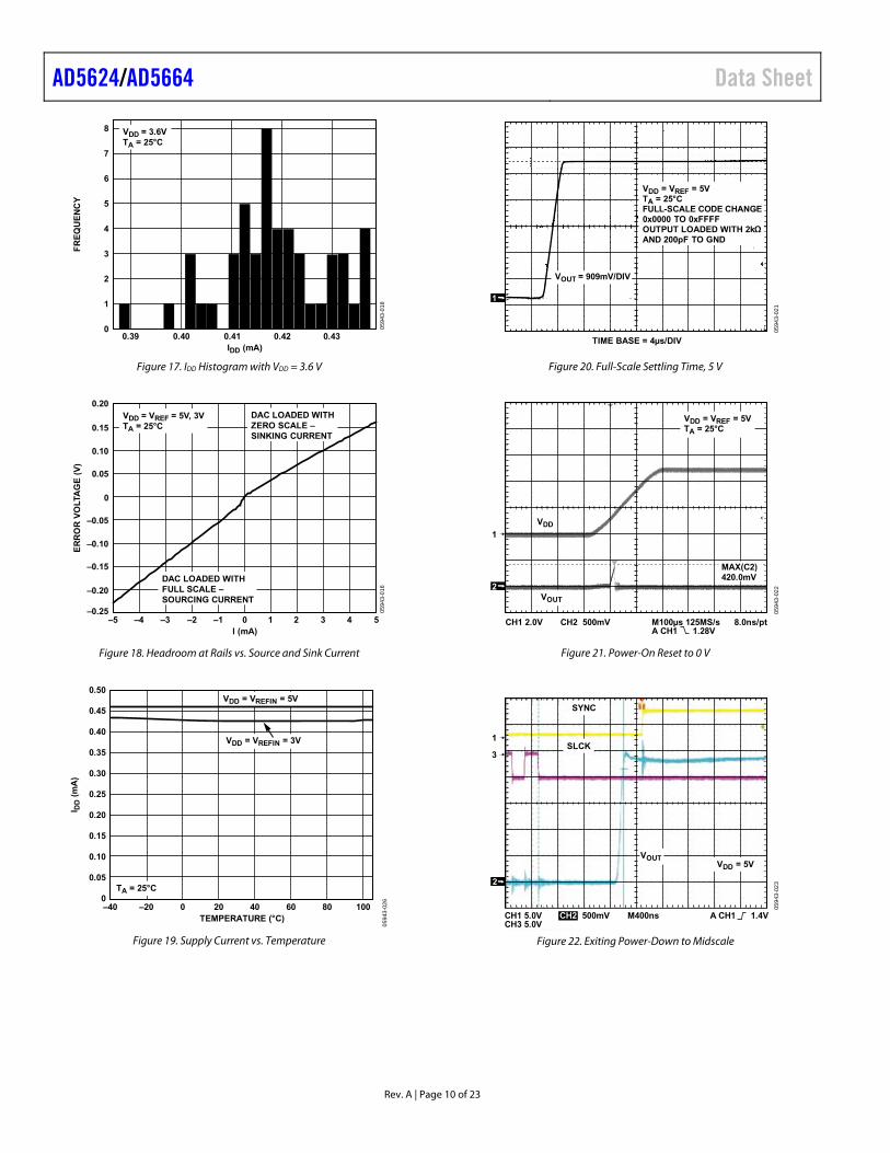
Figure 16. IDD Histogram with VDD = 5.5 V
AD5624/AD5664 Data Sheet
Rev. A | Page 10 of 23
IDD (mA)
FR
EQ
UE
NC
Y
0
1
2
3
5
4
6
8
7
0.39 0.40 0.41 0.42 0.43
0594
3-01
8
VDD = 3.6VTA = 25°C
Figure 17. IDD Histogram with VDD = 3.6 V
I (mA)
ER
RO
R V
OLT
AG
E (
V)
0.20
–0.25
–0.20
–0.15
–0.10
–0.05
0
0.05
0.10
0.15
–5 –4 –3 –2 –1 0 1 2 43 5
0594
3-01
6
VDD = VREF = 5V, 3VTA = 25°C
DAC LOADED WITHZERO SCALE –SINKING CURRENT
DAC LOADED WITHFULL SCALE –SOURCING CURRENT
Figure 18. Headroom at Rails vs. Source and Sink Current
TEMPERATURE (°C)
I DD
(m
A)
0.50
0.05
0.10
0.15
0.20
0.35
0.40
0.25
0.30
0.45
0–40 –20 0 20 40 60 80 100
0594
3-02
6
TA = 25°C
VDD = VREFIN = 5V
VDD = VREFIN = 3V
Figure 19. Supply Current vs. Temperature
0594
3-02
1
TIME BASE = 4µs/DIV
VDD = VREF = 5VTA = 25°CFULL-SCALE CODE CHANGE0x0000 TO 0xFFFFOUTPUT LOADED WITH 2kΩAND 200pF TO GND
VOUT = 909mV/DIV
1
Figure 20. Full-Scale Settling Time, 5 V
0594
3-02
2
CH1 2.0V CH2 500mV M100µs 125MS/sA CH1 1.28V
8.0ns/pt
VDD = VREF = 5VTA = 25°C
VOUT
VDD
1
2
MAX(C2)420.0mV
Figure 21. Power-On Reset to 0 V
0594
3-02
3
VDD = 5V
SYNC
SLCK
VOUT
1
3
CH1 5.0VCH3 5.0V
CH2 500mV M400ns A CH1 1.4V
2
Figure 22. Exiting Power-Down to Midscale
Data Sheet AD5624/AD5664
Rev. A | Page 11 of 23
SAMPLE NUMBER
VO
UT (
V)
2.521
2.522
2.523
2.524
2.525
2.526
2.527
2.528
2.529
2.530
2.531
2.532
2.533
2.534
2.535
2.536
2.537
2.538
0 50 100 150 350 400200 250 300 450 512
0594
3-02
4
VDD = VREF = 5VTA = 25°C5ns/SAMPLE NUMBERGLITCH IMPULSE = 9.494nV1LSB CHANGE AROUNDMIDSCALE (0x8000 TO 0x7FFF)
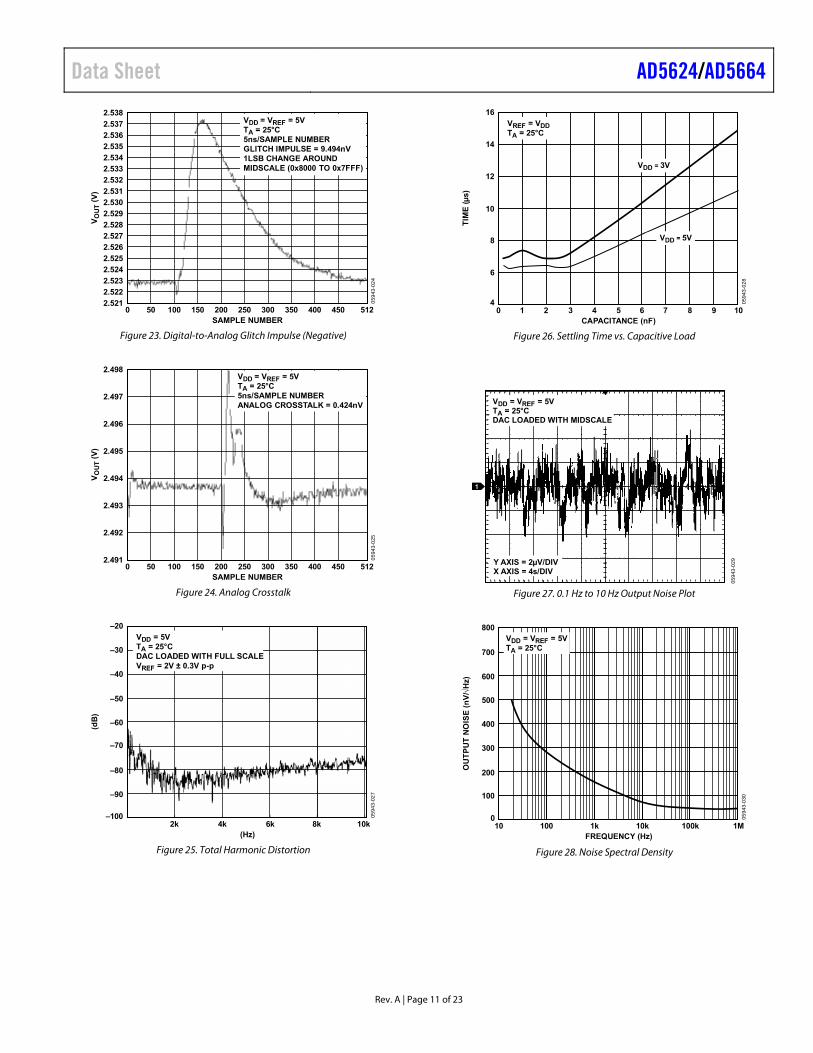
Figure 23. Digital-to-Analog Glitch Impulse (Negative)
SAMPLE NUMBER
VO
UT (
V)
2.491
2.492
2.493
2.494
2.495
2.496
2.497
2.498
0 50 100 150 350 400200 250 300 450 512
0594
3-02
5VDD = VREF = 5VTA = 25°C5ns/SAMPLE NUMBERANALOG CROSSTALK = 0.424nV
Figure 24. Analog Crosstalk
(Hz)
(dB
)
–20
–50
–80
–30
–40
–60
–70
–90
–1002k 4k 6k 8k 10k
0594
3-02
7
VDD = 5VTA = 25°CDAC LOADED WITH FULL SCALEVREF = 2V ± 0.3V p-p
Figure 25. Total Harmonic Distortion
CAPACITANCE (nF)
TIM
E (
µs)
16
14
12
10
8
6
40 1 2 3 4 5 6 7 98 10
0594
3-02
8
VREF = VDDTA = 25°C
VDD = 5V
VDD = 3V
Figure 26. Settling Time vs. Capacitive Load
0594
3-02
9
1
Y AXIS = 2µV/DIVX AXIS = 4s/DIV
VDD = VREF = 5VTA = 25°CDAC LOADED WITH MIDSCALE
Figure 27. 0.1 Hz to 10 Hz Output Noise Plot
FREQUENCY (Hz)
OU
TP
UT
NO
ISE
(n
V/√
Hz)
800
600
700
400
500
100
200
300
010 100k10k1k100 1M
0594
3-03
0
VDD = VREF = 5VTA = 25°C
Figure 28. Noise Spectral Density
AD5624/AD5664 Data Sheet
Rev. A | Page 12 of 23
FREQUENCY (Hz)
(dB
)
5
–4010k 100k 1M 10M
0594
3-03
1–35
–30
–25
–20
–15
–10
–5
0
VDD = 5VTA = 25°C
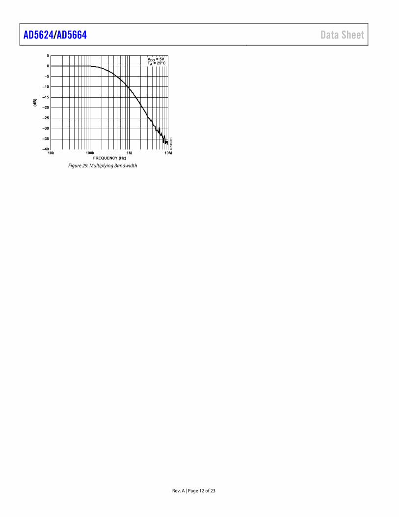
Figure 29. Multiplying Bandwidth
Data Sheet AD5624/AD5664
Rev. A | Page 13 of 23
TERMINOLOGY Relative Accuracy or Integral Nonlinearity (INL) For the DAC, relative accuracy or integral nonlinearity is a measurement of the maximum deviation, in LSBs, from a straight line passing through the endpoints of the DAC transfer function. A typical INL vs. code plot can be seen in Figure 5 and Figure 6.
Differential Nonlinearity (DNL) Differential nonlinearity is the difference between the measured change and the ideal 1 LSB change between any two adjacent codes. A specified differential nonlinearity of ±1 LSB maximum ensures monotonicity. This DAC is guaranteed monotonic by design. A typical DNL vs. code plot can be seen in Figure 7 and Figure 8.
Zero-Scale Error Zero-scale error is a measurement of the output error when zero code (0x0000) is loaded to the DAC register. Ideally, the output is 0 V. The zero code error is always positive in the AD5624/AD5664 because the output of the DAC cannot go below 0 V. It is due to a combination of the offset errors in the DAC and the output amplifier. Zero code error is expressed in mV. A plot of zero code error vs. temperature can be seen in Figure 13.
Full-Scale Error Full-scale error is a measurement of the output error when full-scale code (0xFFFF) is loaded to the DAC register. Ideally, the output is VDD − 1 LSB. Full-scale error is expressed in % of FSR. A plot of full-scale error vs. temperature can be seen in Figure 12.
Gain Error This is a measure of the span error of the DAC. It is the deviation in slope of the DAC transfer characteristic from ideal expressed as a % of FSR.
Zero Code Error Drift This is a measurement of the change in zero code error with a change in temperature. It is expressed in μV/°C.
Gain Temperature Coefficient This is a measurement of the change in gain error with changes in temperature. It is expressed in ppm of FSR/°C.
Offset Error Offset error is a measure of the difference between VOUT (actual) and VOUT (ideal) expressed in mV in the linear region of the transfer function. Offset error is measured on the AD5624/ AD5664 with code 512 loaded in the DAC register. It can be negative or positive.
DC Power Supply Rejection Ratio (PSRR) This indicates how the output of the DAC is affected by changes in the supply voltage. PSRR is the ratio of the change in VOUT to a change in VDD for full-scale output of the DAC. It is measured in dB. VREF is held at 2 V, and VDD is varied by ±10%.
Output Voltage Settling Time This is the amount of time it takes for the output of a DAC to settle to a specified level for a ¼ to ¾ full-scale input change and is measured from the 24th falling edge of SCLK.
Digital-to-Analog Glitch Impulse Digital-to-analog glitch impulse is the impulse injected into the analog output when the input code in the DAC register changes state. It is normally specified as the area of the glitch in nV-s, and is measured when the digital input code is changed by 1 LSB at the major carry transition (0x7FFF to 0x8000) as shown in Figure 23.
Digital Feedthrough Digital feedthrough is a measure of the impulse injected into the analog output of the DAC from the digital inputs of the DAC, but is measured when the DAC output is not updated. It is specified in nV-s, and measured with a full-scale code change on the data bus, that is, from all 0s to all 1s and vice versa.
Total Harmonic Distortion (THD) This is the difference between an ideal sine wave and its attenuated version using the DAC. The sine wave is used as the reference for the DAC, and the THD is a measurement of the harmonics present on the DAC output. It is measured in dB.
Noise Spectral Density This is a measurement of the internally generated random noise. Random noise is characterized as a spectral density (nV/√Hz). It is measured by loading the DAC to midscale and measuring noise at the output. It is measured in nV/√Hz. A plot of noise spectral density can be seen in Figure 28.
DC Crosstalk DC crosstalk is the dc change in the output level of one DAC in response to a change in the output of another DAC. It is measured with a full-scale output change on one DAC (or soft power-down and power-up) while monitoring another DAC kept at midscale. It is expressed in μV.
DC crosstalk due to load current change is a measure of the impact that a change in load current on one DAC has to another DAC kept at midscale. It is expressed in μV/mA.
AD5624/AD5664 Data Sheet
Rev. A | Page 14 of 23
Digital Crosstalk
This is the glitch impulse transferred to the output of one DAC at midscale in response to a full-scale code change (all 0s to all 1s and vice versa) in the input register of another DAC. It is measured in standalone mode and is expressed in nV-s.
Analog Crosstalk This is the glitch impulse transferred to the output of one DAC due to a change in the output of another DAC. It is measured by loading one of the input registers with a full-scale code change (all 0s to all 1s and vice versa). Then execute a software LDAC and monitor the output of the DAC whose digital code was not changed. The area of the glitch is expressed in nV-s (see Figure 24).
DAC-to-DAC Crosstalk This is the glitch impulse transferred to the output of one DAC due to a digital code change and subsequent analog output change of another DAC. It is measured by loading the attack channel with a full-scale code change (all 0s to all 1s and vice versa) using the command write to and update while monitoring the output of the victim channel that is at midscale. The energy of the glitch is expressed in nV-s.
Multiplying Bandwidth The amplifiers within the DAC have a finite bandwidth. The multiplying bandwidth is a measure of this. A sine wave on the reference (with full-scale code loaded to the DAC) appears on the output. The multiplying bandwidth is the frequency at which the output amplitude falls to 3 dB below the input.
Data Sheet AD5624/AD5664
Rev. A | Page 15 of 23
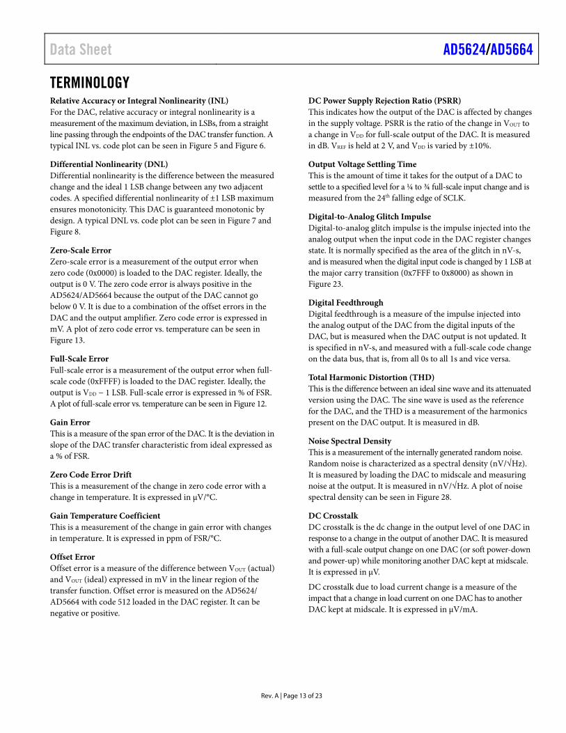
THEORY OF OPERATION D/A SECTION The AD5624/AD5664 DACs are fabricated on a CMOS process. The architecture consists of a string DAC followed by an output buffer amplifier. Figure 30 shows a block diagram of the DAC architecture.
DACREGISTER
RESISTORSTRING
REF (+)
VDD
GND
REF (–)
VOUT
OUTPUTAMPLIFIER(GAIN = +2)
0594
3-03
2
Figure 30. DAC Architecture
Since the input coding to the DAC is straight binary, the ideal output voltage is given by
NREFINOUT
DVV2
where:
D is the decimal equivalent of the binary code that is loaded to the DAC register:
0 to 4095 for AD5624 (12 bit). 0 to 65535 for AD5664 (16 bit).
N is the DAC resolution.
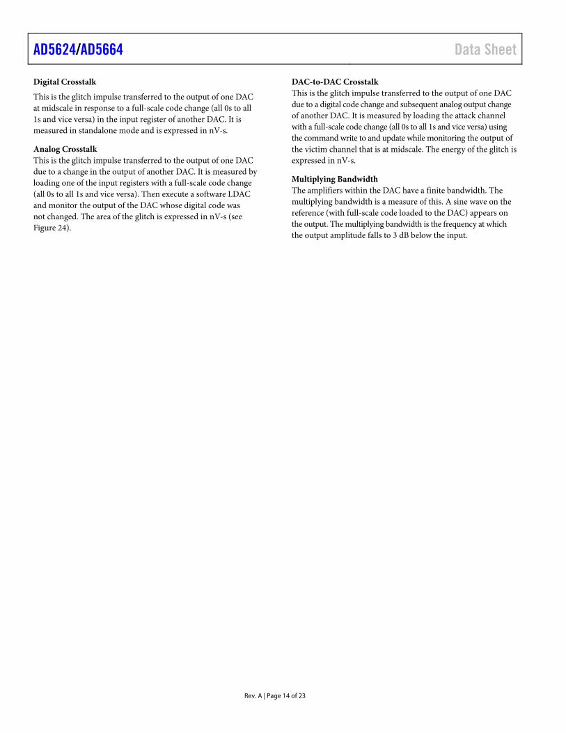
RESISTOR STRING The resistor string is shown in Figure 31. It is simply a string of resistors, each of value R. The code loaded to the DAC register determines at which node on the string the voltage is tapped off to be fed into the output amplifier. The voltage is tapped off by closing one of the switches connecting the string to the amplifier. Because it is a string of resistors, it is guaranteed monotonic.
OUTPUT AMPLIFIER The output buffer amplifier can generate rail-to-rail voltages on its output, which gives an output range of 0 V to VDD. It can drive a load of 2 kΩ in parallel with 1000 pF to GND. The source and sink capabilities of the output amplifier can be seen in Figure 18. The slew rate is 1.8 V/μs with a ¼ to ¾ full-scale settling time of 7 μs.
R
R
R
R
R TO OUTPUTAMPLIFIER
0594
3-03
3
Figure 31. Resistor String
SERIAL INTERFACE The AD5624/AD5664 have a 3-wire serial interface (SYNC, SCLK, and DIN) that is compatible with SPI, QSPI, and MICROWIRE interface standards as well as with most DSPs. See Figure 2 for a timing diagram of a typical write sequence.
The write sequence begins by bringing the SYNC line low. Data from the DIN line is clocked into the 24-bit shift register on the falling edge of SCLK. The serial clock frequency can be as high as 50 MHz, making the AD5624/AD5664 compatible with high speed DSPs. On the 24th falling clock edge, the last data bit is clocked in and the programmed function is executed, that is, a change in DAC register contents and/or a change in the mode of operation. At this stage, the SYNC line can be kept low or be brought high. In either case, it must be brought high for a minimum of 15 ns before the next write sequence so that a falling edge of SYNC can initiate the next write sequence. Because the SYNC buffer draws more current when VIN = 2.0 V than it does when VIN = 0.8 V, SYNC is idled low between write sequences for even lower power operation. It must, however, be brought high again just before the next write sequence.
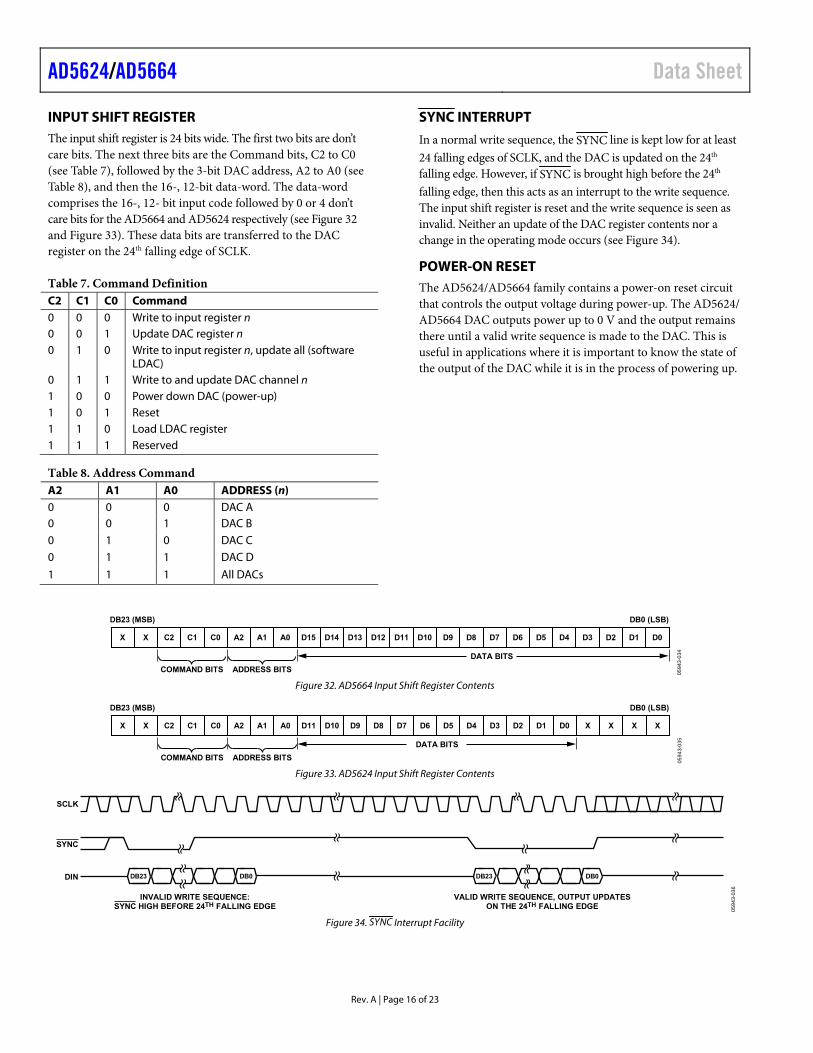
AD5624/AD5664 Data Sheet
Rev. A | Page 16 of 23
INPUT SHIFT REGISTER The input shift register is 24 bits wide. The first two bits are don’t care bits. The next three bits are the Command bits, C2 to C0 (see Table 7), followed by the 3-bit DAC address, A2 to A0 (see Table 8), and then the 16-, 12-bit data-word. The data-word comprises the 16-, 12- bit input code followed by 0 or 4 don’t care bits for the AD5664 and AD5624 respectively (see Figure 32 and Figure 33). These data bits are transferred to the DAC register on the 24th falling edge of SCLK.
Table 7. Command Definition C2 C1 C0 Command 0 0 0 Write to input register n 0 0 1 Update DAC register n 0 1 0 Write to input register n, update all (software
LDAC) 0 1 1 Write to and update DAC channel n 1 0 0 Power down DAC (power-up) 1 0 1 Reset 1 1 0 Load LDAC register 1 1 1 Reserved
Table 8. Address Command A2 A1 A0 ADDRESS (n) 0 0 0 DAC A0 0 1 DAC B0 1 0 DAC C0 1 1 DAC D
1 1 1 All DACs
SYNC INTERRUPT
In a normal write sequence, the SYNC line is kept low for at least 24 falling edges of SCLK, and the DAC is updated on the 24th falling edge. However, if SYNC is brought high before the 24th falling edge, then this acts as an interrupt to the write sequence. The input shift register is reset and the write sequence is seen as invalid. Neither an update of the DAC register contents nor a change in the operating mode occurs (see Figure 34).
POWER-ON RESET The AD5624/AD5664 family contains a power-on reset circuit that controls the output voltage during power-up. The AD5624/ AD5664 DAC outputs power up to 0 V and the output remains there until a valid write sequence is made to the DAC. This is useful in applications where it is important to know the state of the output of the DAC while it is in the process of powering up.
X X C2 C1 C0 A2 A1 A0 D15 D14 D13 D12 D11 D10 D9 D8 D7 D6 D5 D4 D3 D2 D1 D0
DB23 (MSB) DB0 (LSB)
COMMAND BITS ADDRESS BITS
DATA BITS
0594
3-03
4Figure 32. AD5664 Input Shift Register Contents
X X C2 C1 C0 A2 A1 A0 X X X XD11 D10 D9 D8 D7 D6 D5 D4 D3 D2 D1 D0
DB23 (MSB) DB0 (LSB)
COMMAND BITS ADDRESS BITS
DATA BITS
0594
3-03
5
Figure 33. AD5624 Input Shift Register Contents
DIN DB23 DB23 DB0DB0
VALID WRITE SEQUENCE, OUTPUT UPDATESON THE 24TH FALLING EDGE
SYNC
SCLK
INVALID WRITE SEQUENCE:SYNC HIGH BEFORE 24TH FALLING EDGE 05
943-
036
Figure 34. SYNC Interrupt Facility
Data Sheet AD5624/AD5664
Rev. A | Page 17 of 23
SOFTWARE RESET The AD5624/AD5664 contain a software reset function. Command 110 is reserved for the software reset function (see Table 7). The software reset command contains two reset modes that are software programmable by setting Bit DB0 in the control register. Table 9 shows how the state of the bit corresponds to the software reset modes of operation of the devices.
Table 9. Software Reset Modes for the AD5624/AD5664 DB0 Registers Reset to Zero 0 DAC register
Input shift register 1 (Power-On Reset) DAC register
Input shift register LDAC registerPower-down register
POWER-DOWN MODES The AD5624/AD5664 contain four separate modes of operation. Command 100 is reserved for the power-down function (see Table 7). These modes are software programmable by setting two bits (DB5 and DB4) in the control register. Table 10 shows how the state of the bits corresponds to the mode of operation of the device. All DACs (DAC D to DAC A) can be powered down to the selected mode by setting the corresponding four bits (DB3, DB2, DB1, and DB0) to 1. By executing the same Command 100, any combination of DACs is powered up by setting Bit DB5 and Bit DB4 to normal operation mode. To select which combination of DAC channels to power-up, set the corresponding four bits (DB3, DB2, DB1, and DB0) to 1. See Table 11 for contents of the input shift register during the power-down/power-up operation.
Table 10. Modes of Operation for the AD5624/AD5664 DB5 DB4 Operating Mode0 0 Normal operation
Power-down modes0 1 1 kΩ to GND 1 0 100 kΩ to GND 1 1 Three-state
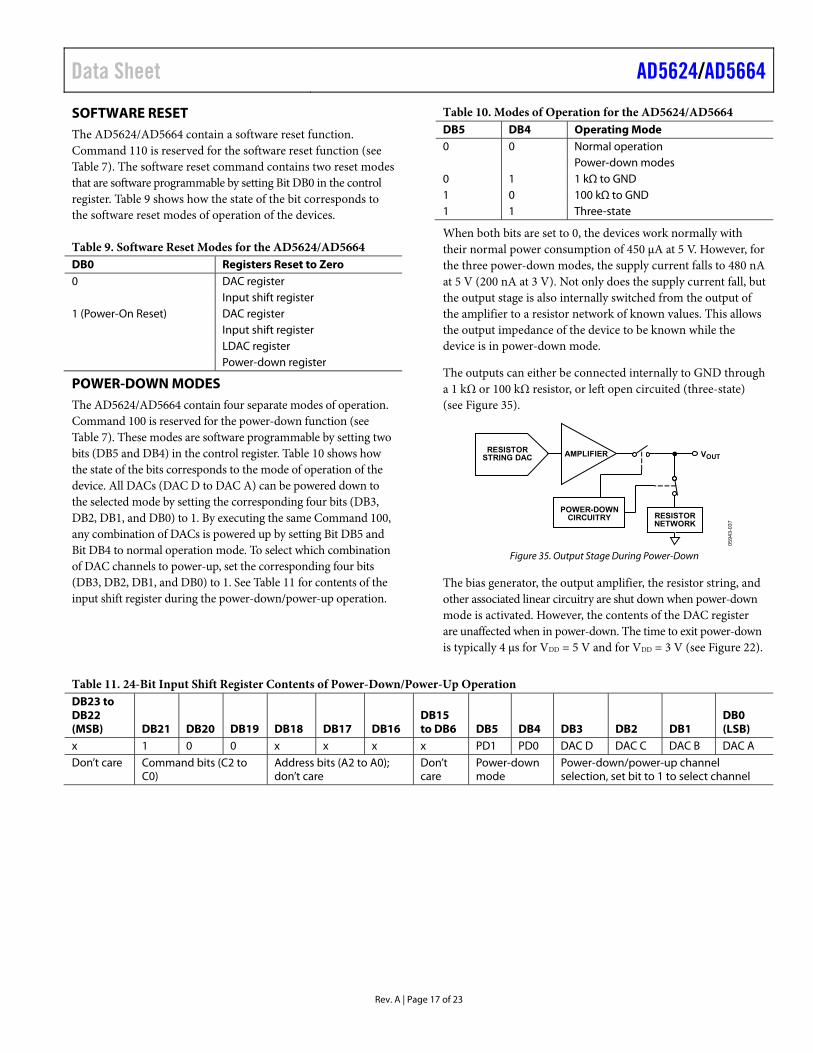
When both bits are set to 0, the devices work normally with their normal power consumption of 450 μA at 5 V. However, for the three power-down modes, the supply current falls to 480 nA at 5 V (200 nA at 3 V). Not only does the supply current fall, but the output stage is also internally switched from the output of the amplifier to a resistor network of known values. This allows the output impedance of the device to be known while the device is in power-down mode.
The outputs can either be connected internally to GND through a 1 kΩ or 100 kΩ resistor, or left open circuited (three-state) (see Figure 35).
RESISTORNETWORK
VOUTRESISTOR
STRING DAC
POWER-DOWNCIRCUITRY
AMPLIFIER
0594
3-03
7
Figure 35. Output Stage During Power-Down
The bias generator, the output amplifier, the resistor string, and other associated linear circuitry are shut down when power-down mode is activated. However, the contents of the DAC register are unaffected when in power-down. The time to exit power-down is typically 4 μs for VDD = 5 V and for VDD = 3 V (see Figure 22).
Table 11. 24-Bit Input Shift Register Contents of Power-Down/Power-Up Operation DB23 to DB22 (MSB) DB21 DB20 DB19 DB18 DB17 DB16
DB15 to DB6 DB5 DB4 DB3 DB2 DB1
DB0 (LSB)
x 1 0 0 x x x x PD1 PD0 DAC D DAC C DAC B DAC A Don’t care Command bits (C2 to
C0) Address bits (A2 to A0); don’t care
Don’t care
Power-down mode
Power-down/power-up channel selection, set bit to 1 to select channel
AD5624/AD5664 Data Sheet
Rev. A | Page 18 of 23
LDAC FUNCTION The AD5624/AD5664 DACs have double buffered interfaces consisting of two banks of registers: input registers and DAC registers. The input registers are connected directly to the input shift register and the digital code is transferred to the relevant input register on completion of a valid write sequence. The DAC registers contain the digital code used by the resistor strings.
The double buffered interface is useful if the user requires simultaneous updating of all DAC outputs. The user can write to three of the input registers individually and then write to the remaining input register and update all DAC registers, the outputs update simultaneously. Command 010 is reserved for this software LDAC.
Access to the DAC registers is controlled by the LDAC function. The LDAC registers contain two modes of operation for each DAC channel. The DAC channels are selected by setting the bits of the 4-bit LDAC register (DB3, DB2, DB1, and DB0). Command 110 is reserved for setting up the LDAC register. When the LDAC bit register is set low, the corresponding DAC registers are latched and the input registers can change state without affecting the contents of the
DAC registers. When the LDAC bit register is set high, however, the DAC registers become transparent and the contents of the input registers are transferred to them on the falling edge of the 24th SCLK pulse. This is equivalent to having an LDAC hardware pin tied permanently low for the selected DAC channel, that is, synchronous update mode. See Table 12 for the LDAC register mode of operation. See Table 13 for contents of the input shift register during the LDAC register set up command.
This flexibility is useful in applications where the user wants to update select channels simultaneously, while the rest of the channels update synchronously.
Table 12. LDAC Register Mode of Operation Load DAC Register
LDAC Bits (DB3 to DB0) LDAC Mode of Operation 0 Normal operation (default), DAC
register update is controlled by write command.
1 The DAC registers are updated after new data is read in on the falling edge of the 24th SCLK pulse.
Table 13. 24-Bit Input Shift Register Contents for LDAC Setup Command for the AD5624/AD5664
DB23 to DB22 (MSB) DB21 DB20 DB19 DB18 DB17 DB16 DB15 to DB4 DB3 DB2 DB1 DB0 (LSB) x 1 1 0 x x x x DACD DACC DACB DACA Don’t care Command bits (C2 to C0) Address bits (A3 to A0);
don’t care Don’t care Set bit to 0 or 1 for required mode
of operation on respective channel
Data Sheet AD5624/AD5664
Rev. A | Page 19 of 23
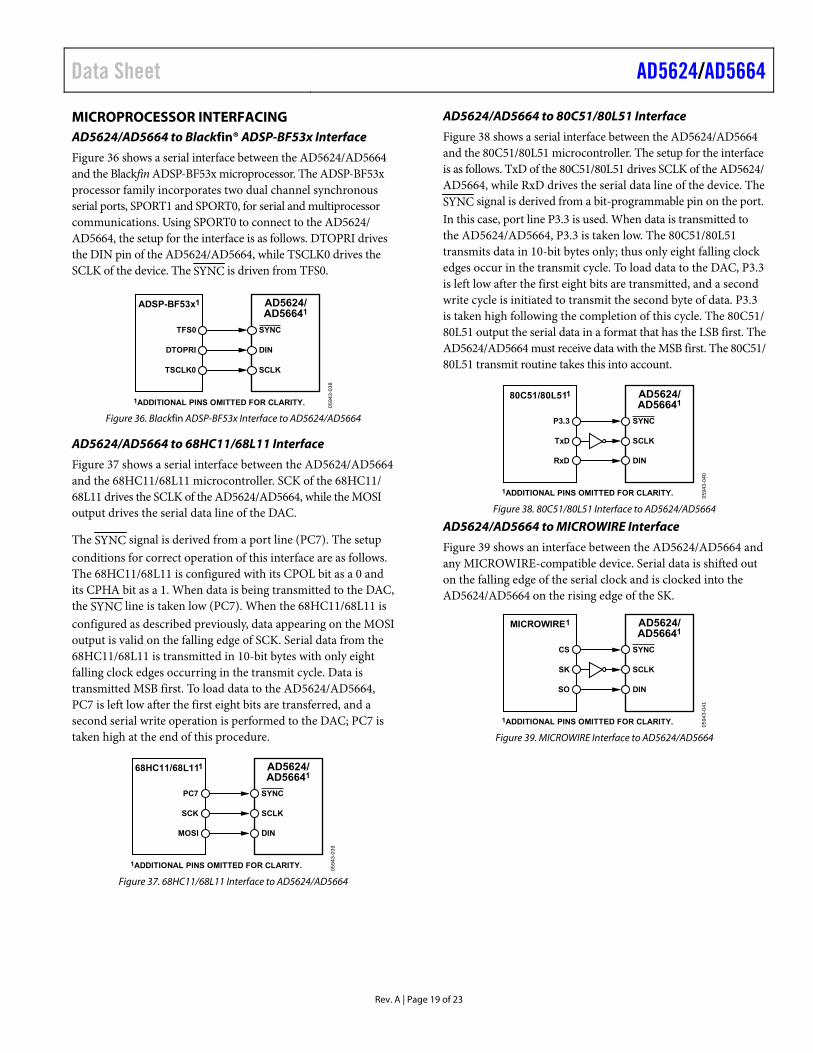
MICROPROCESSOR INTERFACING AD5624/AD5664 to Blackfin® ADSP-BF53x Interface
Figure 36 shows a serial interface between the AD5624/AD5664 and the Blackfin ADSP-BF53x microprocessor. The ADSP-BF53x processor family incorporates two dual channel synchronous serial ports, SPORT1 and SPORT0, for serial and multiprocessor communications. Using SPORT0 to connect to the AD5624/ AD5664, the setup for the interface is as follows. DTOPRI drives the DIN pin of the AD5624/AD5664, while TSCLK0 drives the SCLK of the device. The SYNC is driven from TFS0.
AD5624/AD56641
ADSP-BF53x1
SYNCTFS0
DINDTOPRI
SCLKTSCLK0
1ADDITIONAL PINS OMITTED FOR CLARITY. 0594
3-03
8
Figure 36. Blackfin ADSP-BF53x Interface to AD5624/AD5664
AD5624/AD5664 to 68HC11/68L11 Interface
Figure 37 shows a serial interface between the AD5624/AD5664 and the 68HC11/68L11 microcontroller. SCK of the 68HC11/ 68L11 drives the SCLK of the AD5624/AD5664, while the MOSI output drives the serial data line of the DAC.
The SYNC signal is derived from a port line (PC7). The setup conditions for correct operation of this interface are as follows. The 68HC11/68L11 is configured with its CPOL bit as a 0 and its CPHA bit as a 1. When data is being transmitted to the DAC, the SYNC line is taken low (PC7). When the 68HC11/68L11 is configured as described previously, data appearing on the MOSI output is valid on the falling edge of SCK. Serial data from the 68HC11/68L11 is transmitted in 10-bit bytes with only eight falling clock edges occurring in the transmit cycle. Data is transmitted MSB first. To load data to the AD5624/AD5664, PC7 is left low after the first eight bits are transferred, and a second serial write operation is performed to the DAC; PC7 is taken high at the end of this procedure.
AD5624/AD56641
68HC11/68L111
SYNCPC7
SCLKSCK
DINMOSI
1ADDITIONAL PINS OMITTED FOR CLARITY. 0594
3-03
9
Figure 37. 68HC11/68L11 Interface to AD5624/AD5664
AD5624/AD5664 to 80C51/80L51 Interface
Figure 38 shows a serial interface between the AD5624/AD5664 and the 80C51/80L51 microcontroller. The setup for the interface is as follows. TxD of the 80C51/80L51 drives SCLK of the AD5624/ AD5664, while RxD drives the serial data line of the device. The SYNC signal is derived from a bit-programmable pin on the port. In this case, port line P3.3 is used. When data is transmitted to the AD5624/AD5664, P3.3 is taken low. The 80C51/80L51 transmits data in 10-bit bytes only; thus only eight falling clock edges occur in the transmit cycle. To load data to the DAC, P3.3 is left low after the first eight bits are transmitted, and a second write cycle is initiated to transmit the second byte of data. P3.3 is taken high following the completion of this cycle. The 80C51/ 80L51 output the serial data in a format that has the LSB first. The AD5624/AD5664 must receive data with the MSB first. The 80C51/ 80L51 transmit routine takes this into account.
AD5624/AD56641
80C51/80L511
SYNCP3.3
SCLKTxD
DINRxD
1ADDITIONAL PINS OMITTED FOR CLARITY. 0594
3-04
0
Figure 38. 80C51/80L51 Interface to AD5624/AD5664
AD5624/AD5664 to MICROWIRE Interface
Figure 39 shows an interface between the AD5624/AD5664 and any MICROWIRE-compatible device. Serial data is shifted out on the falling edge of the serial clock and is clocked into the AD5624/AD5664 on the rising edge of the SK.
AD5624/AD56641
MICROWIRE1
SYNCCS
SCLKSK
DINSO
1ADDITIONAL PINS OMITTED FOR CLARITY. 0594
3-04
1
Figure 39. MICROWIRE Interface to AD5624/AD5664
AD5624/AD5664 Data Sheet
Rev. A | Page 20 of 23
APPLICATIONS INFORMATION CHOOSING A REFERENCE FOR THE AD5624/AD5664 To achieve the optimum performance from the AD5624/ AD5664, give thought to the choice of a precision voltage reference. The AD5624/AD5664 have only one reference input, VREF. The voltage on the reference input is used to supply the positive input to the DAC. Therefore, any error in the reference is reflected in the DAC.
When choosing a voltage reference for high accuracy applica-tions, the sources of error are initial accuracy, ppm drift, long term drift, and output voltage noise. Initial accuracy on the output voltage of the DAC leads to a full-scale error in the DAC. To minimize these errors, a reference with high initial accuracy is preferred. Choosing a reference with an output trim adjustment, such as the ADR423, allows a system designer to trim out system errors by setting a reference voltage to a voltage other than the nominal. The trim adjustment can also be used at temperature to trim out any error.
Long term drift is a measurement of how much the reference drifts over time. A reference with a tight long-term drift specification ensures that the overall solution remains relatively stable during its entire lifetime.
The temperature coefficient of a reference’s output voltage affects INL, DNL, and TUE. Choose a reference with a tight temperature coefficient specification to reduce temperature dependence of the DAC output voltage in ambient conditions.
In high accuracy applications, which have a relatively low noise budget, reference output voltage noise needs to be considered. It is important to choose a reference with as low an output noise voltage as practical for the system noise resolution required. Precision voltage references such as the ADR425 produce low output noise in the 0.1 Hz to10 Hz range. Examples of recom-mended precision references for use as supply to the AD5624/ AD5664 are shown in the Table 14.
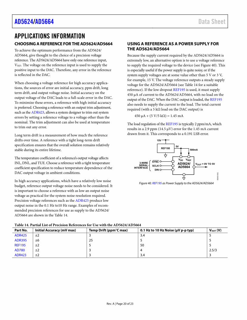
USING A REFERENCE AS A POWER SUPPLY FOR THE AD5624/AD5664 Because the supply current required by the AD5624/AD5664 is extremely low, an alternative option is to use a voltage reference to supply the required voltage to the device (see Figure 40). This is especially useful if the power supply is quite noisy, or if the system supply voltages are at some value other than 5 V or 3 V, for example, 15 V. The voltage reference outputs a steady supply voltage for the AD5624/AD5664 (see Table 14 for a suitable reference). If the low dropout REF195 is used, it must supply 450 μA of current to the AD5624/AD5664, with no load on the output of the DAC. When the DAC output is loaded, the REF195 also needs to supply the current to the load. The total current required (with a 5 kΩ load on the DAC output) is
450 μA + (5 V/5 kΩ) = 1.45 mA
The load regulation of the REF195 is typically 2 ppm/mA, which results in a 2.9 ppm (14.5 μV) error for the 1.45 mA current drawn from it. This corresponds to a 0.191 LSB error.
AD5624/AD5664
3-WIRESERIAL
INTERFACE
SYNC
SCLK
DIN
15V
5V500mA
VOUT = 0V TO 5V
VDD
REF195
VREF
0594
3-04
2
Figure 40. REF195 as Power Supply to the AD5624/AD5664
Table 14. Partial List of Precision References for Use with the AD5624/AD5664 Part No. Initial Accuracy (mV max) Temp Drift (ppm°C max) 0.1 Hz to 10 Hz Noise (μV p-p typ) VOUT (V) ADR425 ±2 3 3.4 5ADR395 ±6 25 5 5REF195 ±2 5 50 5AD780 ±2 3 4 2.5/3ADR423 ±2 3 3.4 3
Data Sheet AD5624/AD5664
Rev. A | Page 21 of 23
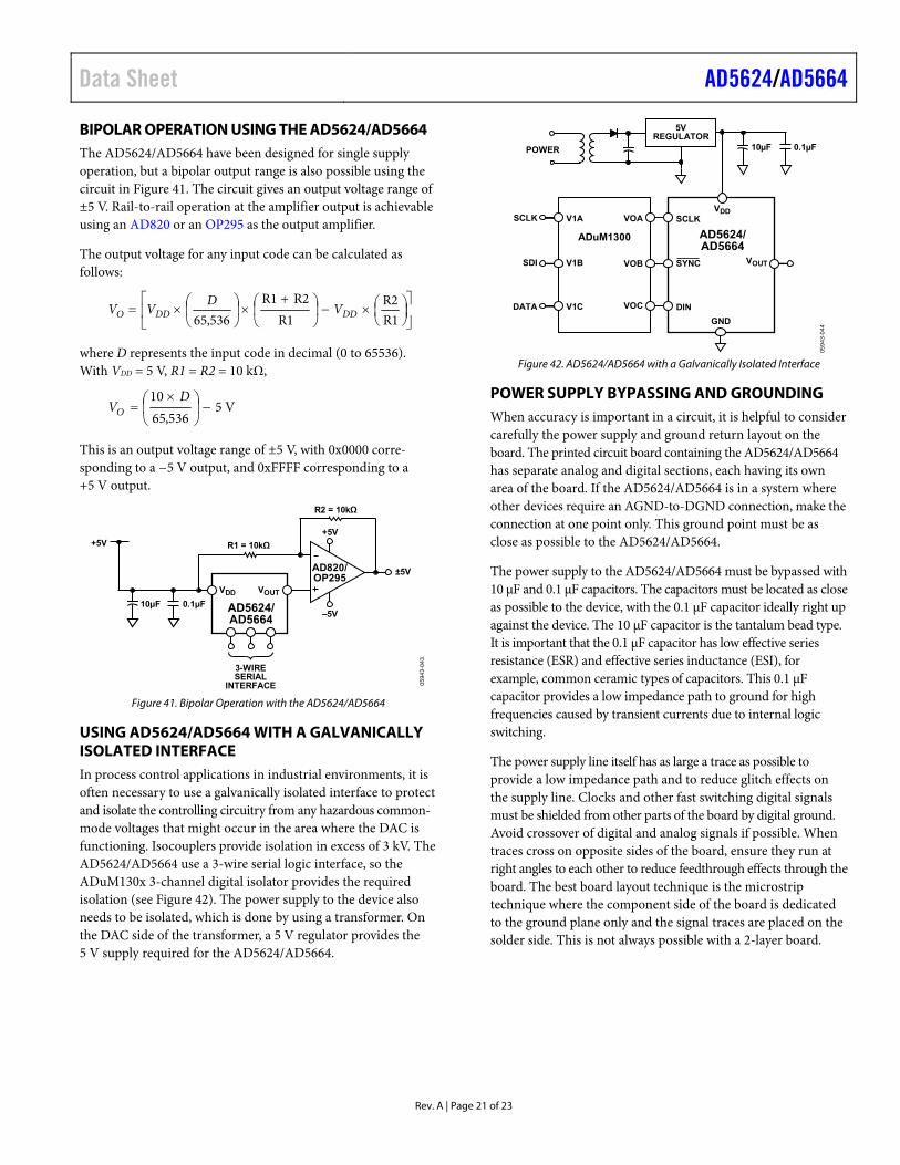
BIPOLAR OPERATION USING THE AD5624/AD5664 The AD5624/AD5664 have been designed for single supply operation, but a bipolar output range is also possible using the circuit in Figure 41. The circuit gives an output voltage range of ±5 V. Rail-to-rail operation at the amplifier output is achievable using an AD820 or an OP295 as the output amplifier.
The output voltage for any input code can be calculated as follows:
R1R2
R1R2R1
536,65 DDDDO VD
VV
where D represents the input code in decimal (0 to 65536). With VDD = 5 V, R1 = R2 = 10 kΩ,
V5536,65
10
DVO
This is an output voltage range of ±5 V, with 0x0000 corre-sponding to a −5 V output, and 0xFFFF corresponding to a +5 V output.
3-WIRESERIAL
INTERFACE
R2 = 10kΩ
+5V
–5V
AD820/OP295
+5V
AD5624/AD5664
VDD VOUT
R1 = 10kΩ
±5V
0.1µF10µF
0594
3-04
3
Figure 41. Bipolar Operation with the AD5624/AD5664
USING AD5624/AD5664 WITH A GALVANICALLY ISOLATED INTERFACE In process control applications in industrial environments, it is often necessary to use a galvanically isolated interface to protect and isolate the controlling circuitry from any hazardous common-mode voltages that might occur in the area where the DAC is functioning. Isocouplers provide isolation in excess of 3 kV. The AD5624/AD5664 use a 3-wire serial logic interface, so the ADuM130x 3-channel digital isolator provides the required isolation (see Figure 42). The power supply to the device also needs to be isolated, which is done by using a transformer. On the DAC side of the transformer, a 5 V regulator provides the 5 V supply required for the AD5624/AD5664.
0.1µF
5VREGULATOR
GND
DIN
SYNC
SCLK
POWER 10µF
SDI
SCLK
DATA
AD5624/AD5664
VOUTVOB
VOA
VOC
VDD
V1C
V1B
V1A
ADuM1300
0594
3-04
4
Figure 42. AD5624/AD5664 with a Galvanically Isolated Interface
POWER SUPPLY BYPASSING AND GROUNDING When accuracy is important in a circuit, it is helpful to consider carefully the power supply and ground return layout on the board. The printed circuit board containing the AD5624/AD5664 has separate analog and digital sections, each having its own area of the board. If the AD5624/AD5664 is in a system where other devices require an AGND-to-DGND connection, make the connection at one point only. This ground point must be as close as possible to the AD5624/AD5664.
The power supply to the AD5624/AD5664 must be bypassed with 10 μF and 0.1 μF capacitors. The capacitors must be located as close as possible to the device, with the 0.1 μF capacitor ideally right up against the device. The 10 μF capacitor is the tantalum bead type. It is important that the 0.1 μF capacitor has low effective series resistance (ESR) and effective series inductance (ESI), for example, common ceramic types of capacitors. This 0.1 μF capacitor provides a low impedance path to ground for high frequencies caused by transient currents due to internal logic switching.
The power supply line itself has as large a trace as possible to provide a low impedance path and to reduce glitch effects on the supply line. Clocks and other fast switching digital signals must be shielded from other parts of the board by digital ground. Avoid crossover of digital and analog signals if possible. When traces cross on opposite sides of the board, ensure they run at right angles to each other to reduce feedthrough effects through the board. The best board layout technique is the microstrip technique where the component side of the board is dedicated to the ground plane only and the signal traces are placed on the solder side. This is not always possible with a 2-layer board.
AD5624/AD5664 Data Sheet
Rev. A | Page 22 of 23
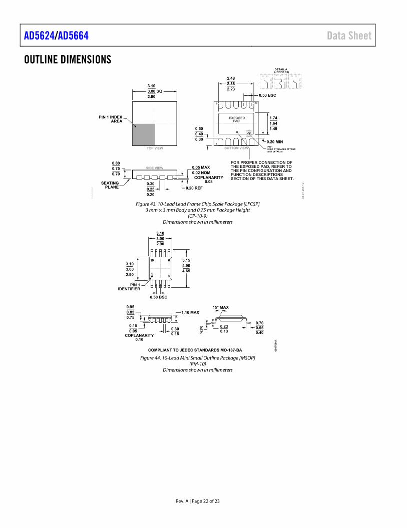
OUTLINE DIMENSIONS 2.482.382.23
0.500.400.30
10
1
6
5
0.300.250.20
PIN 1 INDEXAREA
SEATINGPLANE
0.800.750.70
1.741.641.49
0.20 REF
0.05 MAX0.02 NOM
0.50 BSC
EXPOSEDPAD
3.103.00 SQ2.90
COPLANARITY0.08
TOP VIEW
SIDE VIEW
BOTTOM VIEW
0.20 MIN
PK
G-0
043
62
02-0
7-2
017
-C
FOR PROPER CONNECTION OFTHE EXPOSED PAD, REFER TOTHE PIN CONFIGURATION ANDFUNCTION DESCRIPTIONSSECTION OF THIS DATA SHEET.
PIN 1INDIC ATOR AREA OPTIONS(SEE DETAIL A)
DETAIL A(JEDEC 95)
Figure 43. 10-Lead Lead Frame Chip Scale Package [LFCSP] 3 mm × 3 mm Body and 0.75 mm Package Height
(CP-10-9) Dimensions shown in millimeters
COMPLIANT TO JEDEC STANDARDS MO-187-BA 0917
09-A
6°0°
0.700.550.40
5
10
1
6
0.50 BSC
0.300.15
1.10 MAX
3.103.002.90
COPLANARITY0.10
0.230.13
3.103.002.90
5.154.904.65
PIN 1IDENTIFIER
15° MAX0.950.850.75
0.150.05
Figure 44. 10-Lead Mini Small Outline Package [MSOP] (RM-10)
Dimensions shown in millimeters
Data Sheet AD5624/AD5664
Rev. A | Page 23 of 23
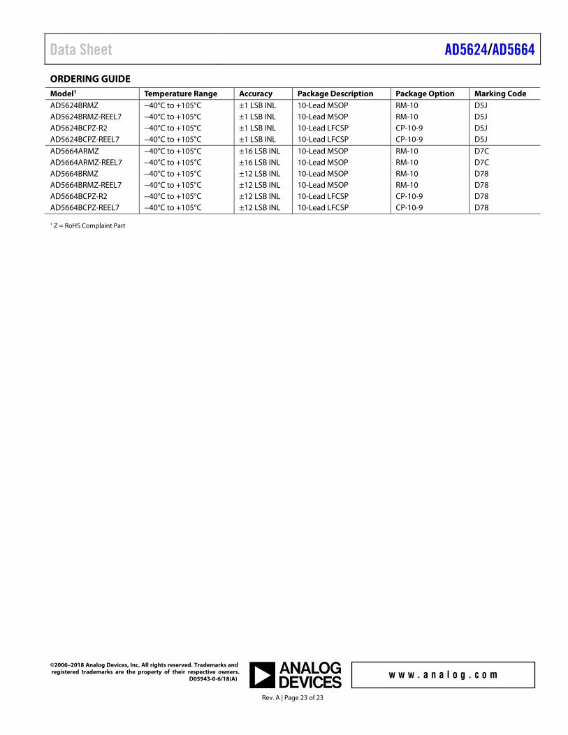
ORDERING GUIDE Model1 Temperature Range Accuracy Package Description Package Option Marking Code AD5624BRMZ −40°C to +105°C ±1 LSB INL 10-Lead MSOP RM-10 D5J AD5624BRMZ-REEL7 −40°C to +105°C ±1 LSB INL 10-Lead MSOP RM-10 D5J AD5624BCPZ-R2 −40°C to +105°C ±1 LSB INL 10-Lead LFCSP CP-10-9 D5J AD5624BCPZ-REEL7 −40°C to +105°C ±1 LSB INL 10-Lead LFCSP CP-10-9 D5J AD5664ARMZ −40°C to +105°C ±16 LSB INL 10-Lead MSOP RM-10 D7C AD5664ARMZ-REEL7 −40°C to +105°C ±16 LSB INL 10-Lead MSOP RM-10 D7C AD5664BRMZ −40°C to +105°C ±12 LSB INL 10-Lead MSOP RM-10 D78 AD5664BRMZ-REEL7 −40°C to +105°C ±12 LSB INL 10-Lead MSOP RM-10 D78 AD5664BCPZ-R2 −40°C to +105°C ±12 LSB INL 10-Lead LFCSP CP-10-9 D78 AD5664BCPZ-REEL7 −40°C to +105°C ±12 LSB INL 10-Lead LFCSP CP-10-9 D78
1 Z = RoHS Complaint Part
©2006–2018 Analog Devices, Inc. All rights reserved. Trademarks and registered trademarks are the property of their respective owners.
D05943-0-6/18(A)


![60 NJU7056/NJU7057/NJU7058 V] 1 Rail-to-Rail … Low Noise, Low Offset Voltage Drift Rail-to-Rail Output CMOS Operational Amplifier FEATURES(V+=5V, V-=0V, Ta=25 C) GENERA](https://img.pdfslide.us/doc/110x75/5ae3c5997f8b9a595d8edf03/60-nju7056nju7057nju7058-v-1-rail-to-rail-low-noise-low-offset-voltage-drift.jpg)