Embed Size (px)
Citation preview
30 V, Micropower, Overvoltage Protection, Rail-to-Rail Input/Output Amplifiers
Data Sheet ADA4096-2/ADA4096-4
Rev. G Document Feedback Information furnished by Analog Devices is believed to be accurate and reliable. However, no responsibility is assumed by Analog Devices for its use, nor for any infringements of patents or other rights of third parties that may result from its use. Specifications subject to change without notice. No license is granted by implication or otherwise under any patent or patent rights of Analog Devices. Trademarks and registered trademarks are the property of their respective owners.
One Technology Way, P.O. Box 9106, Norwood, MA 02062-9106, U.S.A. Tel: 781.329.4700 ©2011–2017 Analog Devices, Inc. All rights reserved. Technical Support www.analog.com
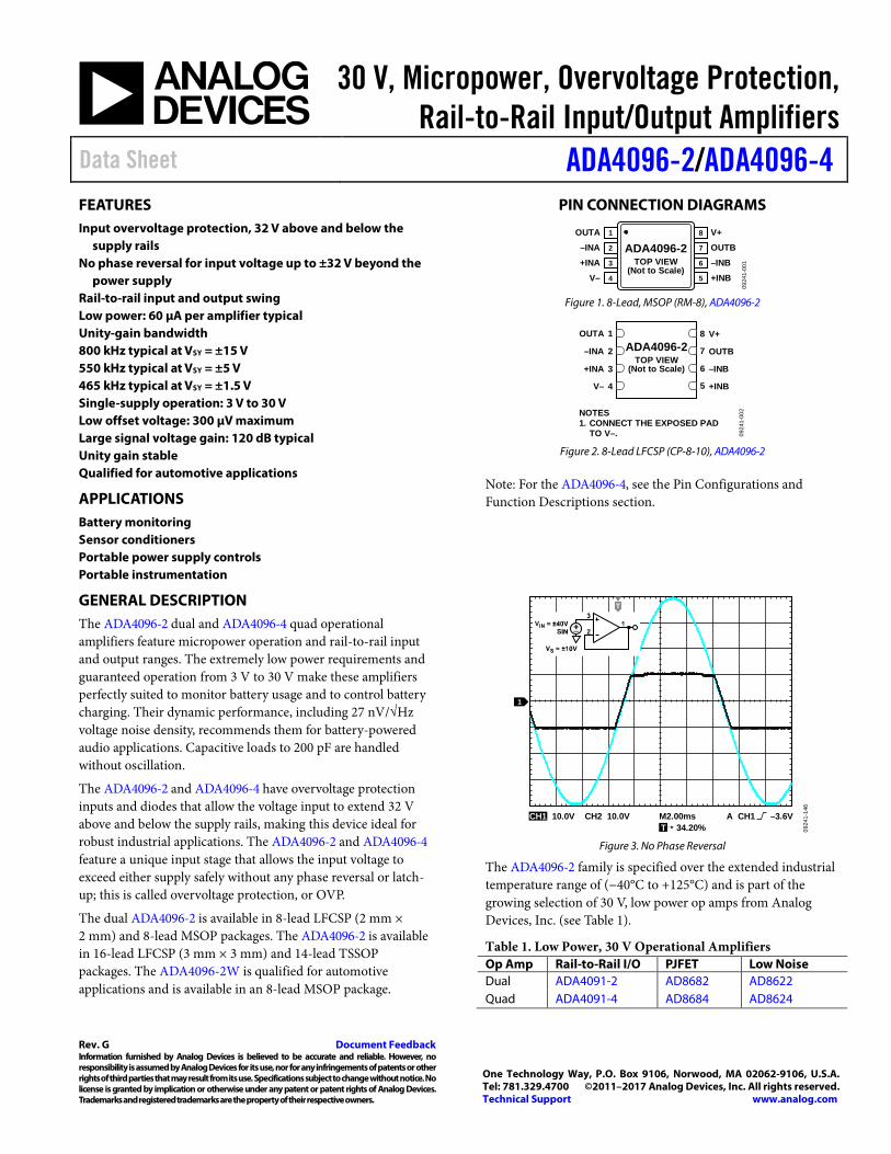
FEATURES Input overvoltage protection, 32 V above and below the
supply rails No phase reversal for input voltage up to ±32 V beyond the
power supply Rail-to-rail input and output swing Low power: 60 µA per amplifier typical Unity-gain bandwidth 800 kHz typical at VSY = ±15 V 550 kHz typical at VSY = ±5 V 465 kHz typical at VSY = ±1.5 V Single-supply operation: 3 V to 30 V Low offset voltage: 300 µV maximum Large signal voltage gain: 120 dB typical Unity gain stable Qualified for automotive applications
APPLICATIONS Battery monitoring Sensor conditioners Portable power supply controls Portable instrumentation
PIN CONNECTION DIAGRAMS
OUTA 1
–INA 2
+INA 3
V– 4
V+8
OUTB7
–INB6
+INB5
ADA4096-2TOP VIEW
(Not to Scale)
0924
1-00
1
Figure 1. 8-Lead, MSOP (RM-8), ADA4096-2
V+
OUTB
–INB
+INB
ADA4096-2TOP VIEW
(Not to Scale)3+INA
4V–
1OUTA
2–INA
6
5
8
7
NOTES1. CONNECT THE EXPOSED PAD
TO V–. 0924
1-00
2
Figure 2. 8-Lead LFCSP (CP-8-10), ADA4096-2
Note: For the ADA4096-4, see the Pin Configurations and Function Descriptions section.
GENERAL DESCRIPTION The ADA4096-2 dual and ADA4096-4 quad operational amplifiers feature micropower operation and rail-to-rail input and output ranges. The extremely low power requirements and guaranteed operation from 3 V to 30 V make these amplifiers perfectly suited to monitor battery usage and to control battery charging. Their dynamic performance, including 27 nV/√Hz voltage noise density, recommends them for battery-powered audio applications. Capacitive loads to 200 pF are handled without oscillation.
The ADA4096-2 and ADA4096-4 have overvoltage protection inputs and diodes that allow the voltage input to extend 32 V above and below the supply rails, making this device ideal for robust industrial applications. The ADA4096-2 and ADA4096-4 feature a unique input stage that allows the input voltage to exceed either supply safely without any phase reversal or latch-up; this is called overvoltage protection, or OVP.
The dual ADA4096-2 is available in 8-lead LFCSP (2 mm × 2 mm) and 8-lead MSOP packages. The ADA4096-2 is available in 16-lead LFCSP (3 mm × 3 mm) and 14-lead TSSOP packages. The ADA4096-2W is qualified for automotive applications and is available in an 8-lead MSOP package.
CH1 10.0V CH2 10.0V M2.00ms A CH1 –3.6VT 34.20%
1
T
0924
1-14
6
Figure 3. No Phase Reversal
The ADA4096-2 family is specified over the extended industrial temperature range of (−40°C to +125°C) and is part of the growing selection of 30 V, low power op amps from Analog Devices, Inc. (see Table 1).
Table 1. Low Power, 30 V Operational Amplifiers Op Amp Rail-to-Rail I/O PJFET Low Noise Dual ADA4091-2 AD8682 AD8622 Quad ADA4091-4 AD8684 AD8624
ADA4096-2/ADA4096-4 Data Sheet
Rev. G | Page 2 of 25
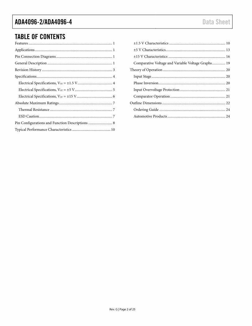
TABLE OF CONTENTS Features .............................................................................................. 1
Applications ....................................................................................... 1
Pin Connection Diagrams ............................................................... 1
General Description ......................................................................... 1
Revision History ............................................................................... 3
Specifications ..................................................................................... 4
Electrical Specifications, VSY = ±1.5 V ....................................... 4
Electrical Specifications, VSY = ±5 V .......................................... 5
Electrical Specifications, VSY = ±15 V ........................................ 6
Absolute Maximum Ratings ............................................................ 7
Thermal Resistance ...................................................................... 7
ESD Caution .................................................................................. 7
Pin Configurations and Function Descriptions ........................... 8
Typical Performance Characteristics ........................................... 10
±1.5 V Characteristics ............................................................... 10
±5 V Characteristics................................................................... 13
±15 V Characteristics ................................................................ 16
Comparative Voltage and Variable Voltage Graphs ............... 19
Theory of Operation ...................................................................... 20
Input Stage ................................................................................... 20
Phase Inversion ........................................................................... 20
Input Overvoltage Protection ................................................... 21
Comparator Operation .............................................................. 21
Outline Dimensions ....................................................................... 22
Ordering Guide .......................................................................... 24
Automotive Products ................................................................. 24
Data Sheet ADA4096-2/ADA4096-4
Rev. G | Page 3 of 25
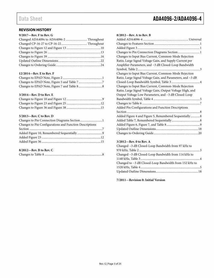
REVISION HISTORY 9/2017—Rev. F to Rev. G Changed ADA409x to ADA4096-2 ............................ Throughout Changed CP-16-27 to CP-16-22 .................................. Throughout Changes to Figure 12 and Figure 13 ............................................. 10 Changes to Figure 26 ...................................................................... 13 Changes to Figure 39 ...................................................................... 16 Updated Outline Dimensions ........................................................ 22 Changes to Ordering Guide ........................................................... 24 12/2014—Rev. E to Rev. F Changes to EPAD Note, Figure 2 .................................................... 1 Changes to EPAD Note, Figure 5 and Table 7 ............................... 7 Changes to EPAD Note, Figure 7 and Table 8 ............................... 8 3/2014—Rev. D to Rev. E Changes to Figure 10 and Figure 12 ............................................... 9 Changes to Figure 23 and Figure 25 ............................................. 12 Changes to Figure 36 and Figure 38 ............................................. 15 5/2013—Rev. C to Rev. D Changes to Pin Connection Diagrams Section ............................. 1 Changes to Pin Configurations and Function Descriptions Section ................................................................................................ 7 Added Figure 10, Renumbered Sequentially ................................. 9 Added Figure 23 .............................................................................. 12 Added Figure 36 .............................................................................. 15 8/2012—Rev. B to Rev. C Changes to Table 8 ............................................................................ 8
8/2012—Rev. A to Rev. B Added ADA4096-4 ............................................................ Universal Changes to Features Section ............................................................ 1 Added Figure 3 .................................................................................. 1 Changes to Pin Connection Diagrams Section ............................. 1 Changes to Input Bias Current, Common-Mode Rejection Ratio, Large Signal Voltage Gain, and Supply Current per Amplifier Parameters, and −3 dB Closed-Loop Bandwidth Symbol, Table 2 .................................................................................. 3 Changes to Input Bias Current, Common-Mode Rejection Ratio, Large Signal Voltage Gain, and Parameters, and −3 dB Closed-Loop Bandwidth Symbol, Table 3 ..................................... 4 Changes to Input Bias Current, Common-Mode Rejection Ratio, Large Signal Voltage Gain, Output Voltage High, and Output Voltage Low Parameters, and −3 dB Closed-Loop Bandwidth Symbol, Table 4 ............................................................. 5 Changes to Table 6 ............................................................................ 7 Added Pin Configurations and Function Descriptions Section ................................................................................................ 8 Added Figure 4 and Figure 5, Renumbered Sequentially ............ 8 Added Table 7, Renumbered Sequentially ..................................... 8 Added Figure 6, Figure 7, and Table 8 ............................................ 9 Updated Outline Dimensions........................................................ 18 Changes to Ordering Guide ........................................................... 20 3/2012—Rev. 0 to Rev. A Changed −3 dB Closed-Loop Bandwidth from 97 kHz to 970 kHz, Table 2 ................................................................................ 3 Changed −3 dB Closed-Loop Bandwidth from 114 kHz to 1140 kHz, Table 3 .............................................................................. 4 Changed to −3 dB Closed-Loop Bandwidth from 152 kHz to 1520 kHz, Table 4 .............................................................................. 5 Updated Outline Dimensions........................................................ 18 7/2011—Revision 0: Initial Version
ADA4096-2/ADA4096-4 Data Sheet
Rev. G | Page 4 of 25
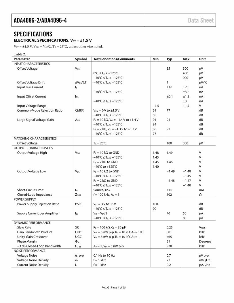
SPECIFICATIONS ELECTRICAL SPECIFICATIONS, VSY = ±1.5 V VSY = ±1.5 V, VCM = VSY/2, TA = 25°C, unless otherwise noted.
Table 2. Parameter Symbol Test Conditions/Comments Min Typ Max Unit INPUT CHARACTERISTICS
Offset Voltage VOS 35 300 µV 0°C ≤ TA ≤ +125°C 450 µV −40°C ≤ TA ≤ +125°C 900 µV Offset Voltage Drift ∆VOS/∆T −40°C ≤ TA ≤ +125°C 1 µV/°C Input Bias Current IB ±10 ±25 nA −40°C ≤ TA ≤ +125°C ±30 nA Input Offset Current IOS ±0.1 ±1.5 nA −40°C ≤ TA ≤ +125°C ±3 nA Input Voltage Range −1.5 +1.5 V Common-Mode Rejection Ratio CMRR VCM = 0 V to ±1.5 V 61 77 dB −40°C ≤ TA ≤ +125°C 58 dB Large Signal Voltage Gain AVO RL = 10 kΩ, VO = −1.4 V to +1.4 V 91 94 dB −40°C ≤ TA ≤ +125°C 84 dB RL = 2 kΩ, VO = −1.3 V to +1.3 V 86 92 dB −40°C ≤ TA ≤ +125°C 77 dB
MATCHING CHARACTERISTICS Offset Voltage TA = 25°C 100 300 µV
OUTPUT CHARACTERISTICS Output Voltage High VOH RL = 10 kΩ to GND 1.48 1.49 V −40°C ≤ TA ≤ +125°C 1.45 V RL = 2 kΩ to GND 1.45 1.46 V −40°C to +125°C 1.40 V Output Voltage Low VOL RL = 10 kΩ to GND −1.49 −1.48 V −40°C ≤ TA ≤ +125°C −1.45 V RL = 2 kΩ to GND −1.48 −1.47 V −40°C ≤ TA ≤ +125°C −1.40 V Short-Circuit Limit ISC Source/sink ±10 mA Closed-Loop Impedance ZOUT f = 100 kHz, AV = 1 102 Ω
POWER SUPPLY Power Supply Rejection Ratio PSRR VSY = 3 V to 36 V 100 dB −40°C ≤ TA ≤ +125°C 90 dB Supply Current per Amplifier ISY VO = VSY/2 40 50 µA −40°C ≤ TA ≤ +125°C 80 µA
DYNAMIC PERFORMANCE Slew Rate SR RL = 100 kΩ, CL = 30 pF 0.25 V/µs Gain Bandwidth Product GBP VIN = 5 mV p-p, RL = 10 kΩ, AV = 100 501 kHz Unity-Gain Crossover UGC VIN = 5 mV p-p, RL = 10 kΩ, AV = 1 465 kHz Phase Margin ΦM 51 Degrees −3 dB Closed-Loop Bandwidth f−3 dB AV = 1, VIN = 5 mV p-p 970 kHz
NOISE PERFORMANCE Voltage Noise en p-p 0.1 Hz to 10 Hz 0.7 µV p-p Voltage Noise Density en f = 1 kHz 27 nV/√Hz Current Noise Density in f = 1 kHz 0.2 pA/√Hz
Data Sheet ADA4096-2/ADA4096-4
Rev. G | Page 5 of 25
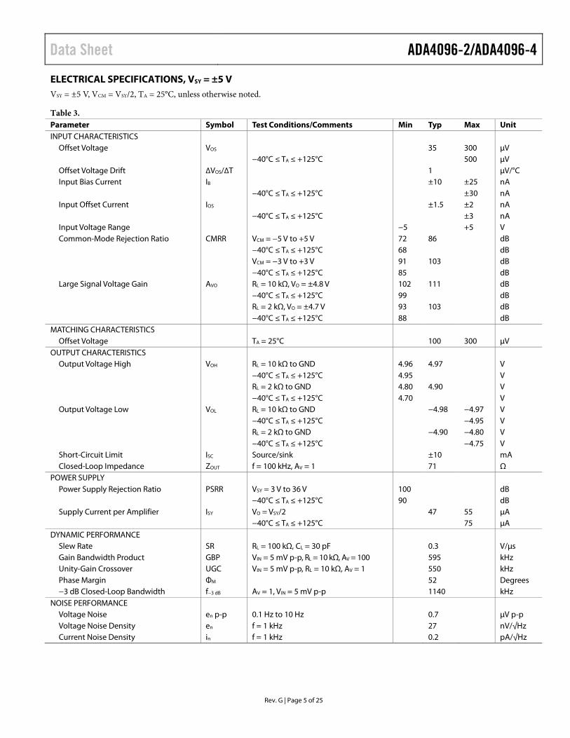
ELECTRICAL SPECIFICATIONS, VSY = ±5 V VSY = ±5 V, VCM = VSY/2, TA = 25°C, unless otherwise noted.
Table 3. Parameter Symbol Test Conditions/Comments Min Typ Max Unit INPUT CHARACTERISTICS
Offset Voltage VOS 35 300 µV −40°C ≤ TA ≤ +125°C 500 µV Offset Voltage Drift ∆VOS/∆T 1 µV/°C Input Bias Current IB ±10 ±25 nA −40°C ≤ TA ≤ +125°C ±30 nA Input Offset Current IOS ±1.5 ±2 nA −40°C ≤ TA ≤ +125°C ±3 nA Input Voltage Range −5 +5 V Common-Mode Rejection Ratio CMRR VCM = −5 V to +5 V 72 86 dB −40°C ≤ TA ≤ +125°C 68 dB VCM = −3 V to +3 V 91 103 dB −40°C ≤ TA ≤ +125°C 85 dB Large Signal Voltage Gain AVO RL = 10 kΩ, VO = ±4.8 V 102 111 dB −40°C ≤ TA ≤ +125°C 99 dB RL = 2 kΩ, VO = ±4.7 V 93 103 dB −40°C ≤ TA ≤ +125°C 88 dB
MATCHING CHARACTERISTICS Offset Voltage TA = 25°C 100 300 µV
OUTPUT CHARACTERISTICS Output Voltage High VOH RL = 10 kΩ to GND 4.96 4.97 V −40°C ≤ TA ≤ +125°C 4.95 V RL = 2 kΩ to GND 4.80 4.90 V −40°C ≤ TA ≤ +125°C 4.70 V Output Voltage Low VOL RL = 10 kΩ to GND −4.98 −4.97 V −40°C ≤ TA ≤ +125°C −4.95 V RL = 2 kΩ to GND −4.90 −4.80 V −40°C ≤ TA ≤ +125°C −4.75 V Short-Circuit Limit ISC Source/sink ±10 mA Closed-Loop Impedance ZOUT f = 100 kHz, AV = 1 71 Ω
POWER SUPPLY Power Supply Rejection Ratio PSRR VSY = 3 V to 36 V 100 dB −40°C ≤ TA ≤ +125°C 90 dB Supply Current per Amplifier ISY VO = VSY/2 47 55 µA −40°C ≤ TA ≤ +125°C 75 µA
DYNAMIC PERFORMANCE Slew Rate SR RL = 100 kΩ, CL = 30 pF 0.3 V/µs Gain Bandwidth Product GBP VIN = 5 mV p-p, RL = 10 kΩ, AV = 100 595 kHz Unity-Gain Crossover UGC VIN = 5 mV p-p, RL = 10 kΩ, AV = 1 550 kHz Phase Margin ΦM 52 Degrees −3 dB Closed-Loop Bandwidth f−3 dB AV = 1, VIN = 5 mV p-p 1140 kHz
NOISE PERFORMANCE Voltage Noise en p-p 0.1 Hz to 10 Hz 0.7 µV p-p Voltage Noise Density en f = 1 kHz 27 nV/√Hz Current Noise Density in f = 1 kHz 0.2 pA/√Hz
ADA4096-2/ADA4096-4 Data Sheet
Rev. G | Page 6 of 25
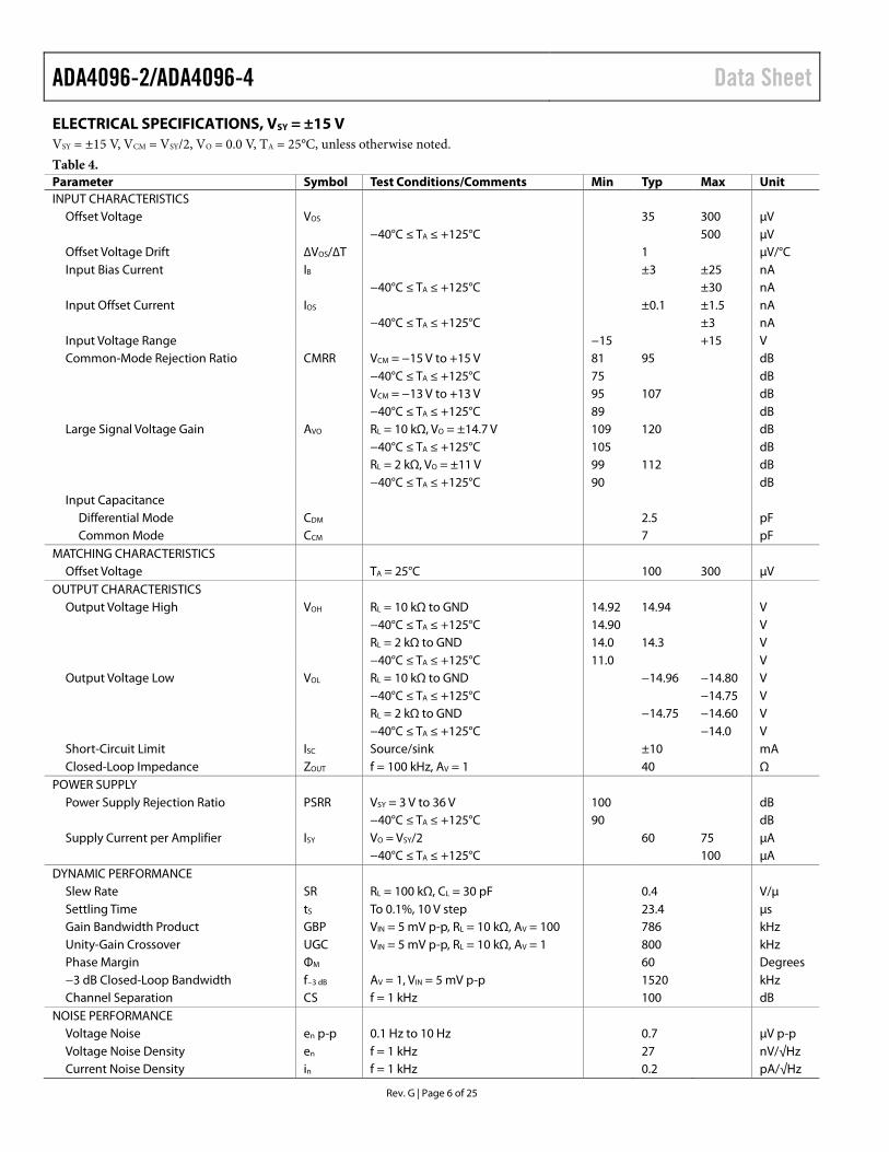
ELECTRICAL SPECIFICATIONS, VSY = ±15 V VSY = ±15 V, VCM = VSY/2, VO = 0.0 V, TA = 25°C, unless otherwise noted. Table 4. Parameter Symbol Test Conditions/Comments Min Typ Max Unit INPUT CHARACTERISTICS
Offset Voltage VOS 35 300 µV −40°C ≤ TA ≤ +125°C 500 µV Offset Voltage Drift ∆VOS/∆T 1 µV/°C Input Bias Current IB ±3 ±25 nA −40°C ≤ TA ≤ +125°C ±30 nA Input Offset Current IOS ±0.1 ±1.5 nA −40°C ≤ TA ≤ +125°C ±3 nA Input Voltage Range −15 +15 V Common-Mode Rejection Ratio CMRR VCM = −15 V to +15 V 81 95 dB −40°C ≤ TA ≤ +125°C 75 dB VCM = −13 V to +13 V 95 107 dB −40°C ≤ TA ≤ +125°C 89 dB Large Signal Voltage Gain AVO RL = 10 kΩ, VO = ±14.7 V 109 120 dB −40°C ≤ TA ≤ +125°C 105 dB RL = 2 kΩ, VO = ±11 V 99 112 dB −40°C ≤ TA ≤ +125°C 90 dB Input Capacitance
Differential Mode CDM 2.5 pF Common Mode CCM 7 pF
MATCHING CHARACTERISTICS Offset Voltage TA = 25°C 100 300 µV
OUTPUT CHARACTERISTICS Output Voltage High VOH RL = 10 kΩ to GND 14.92 14.94 V −40°C ≤ TA ≤ +125°C 14.90 V RL = 2 kΩ to GND 14.0 14.3 V −40°C ≤ TA ≤ +125°C 11.0 V Output Voltage Low VOL RL = 10 kΩ to GND −14.96 −14.80 V −40°C ≤ TA ≤ +125°C −14.75 V RL = 2 kΩ to GND −14.75 −14.60 V −40°C ≤ TA ≤ +125°C −14.0 V Short-Circuit Limit ISC Source/sink ±10 mA Closed-Loop Impedance ZOUT f = 100 kHz, AV = 1 40 Ω
POWER SUPPLY Power Supply Rejection Ratio PSRR VSY = 3 V to 36 V 100 dB −40°C ≤ TA ≤ +125°C 90 dB Supply Current per Amplifier ISY VO = VSY/2 60 75 µA −40°C ≤ TA ≤ +125°C 100 µA
DYNAMIC PERFORMANCE Slew Rate SR RL = 100 kΩ, CL = 30 pF 0.4 V/µ Settling Time tS To 0.1%, 10 V step 23.4 µs Gain Bandwidth Product GBP VIN = 5 mV p-p, RL = 10 kΩ, AV = 100 786 kHz Unity-Gain Crossover UGC VIN = 5 mV p-p, RL = 10 kΩ, AV = 1 800 kHz Phase Margin ΦM 60 Degrees −3 dB Closed-Loop Bandwidth f−3 dB AV = 1, VIN = 5 mV p-p 1520 kHz Channel Separation CS f = 1 kHz 100 dB
NOISE PERFORMANCE Voltage Noise en p-p 0.1 Hz to 10 Hz 0.7 µV p-p Voltage Noise Density en f = 1 kHz 27 nV/√Hz Current Noise Density in f = 1 kHz 0.2 pA/√Hz
Data Sheet ADA4096-2/ADA4096-4
Rev. G | Page 7 of 25
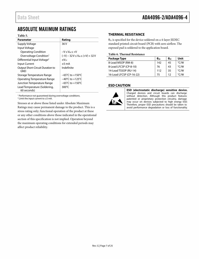
ABSOLUTE MAXIMUM RATINGS Table 5. Parameter Rating Supply Voltage 36 V Input Voltage
Operating Condition −V ≤ VIN ≤ +V Overvoltage Condition1 (−V) − 32 V ≤ VIN ≤ (+V) + 32 V
Differential Input Voltage2 ±VSY Input Current ±5 mA Output Short-Circuit Duration to
GND Indefinite
Storage Temperature Range −65°C to +150°C Operating Temperature Range −40°C to +125°C Junction Temperature Range −65°C to +150°C Lead Temperature (Soldering,
60 seconds) 300°C
1 Performance not guaranteed during overvoltage conditions. 2 Limit the input current to ±5 mA.
Stresses at or above those listed under Absolute Maximum Ratings may cause permanent damage to the product. This is a stress rating only; functional operation of the product at these or any other conditions above those indicated in the operational section of this specification is not implied. Operation beyond the maximum operating conditions for extended periods may affect product reliability.
THERMAL RESISTANCE θJA is specified for the device soldered on a 4-layer JEDEC standard printed circuit board (PCB) with zero airflow. The exposed pad is soldered to the application board.
Table 6. Thermal Resistance Package Type θJA θJC Unit 8-Lead MSOP (RM-8) 142 45 °C/W 8-Lead LFCSP (CP-8-10) 76 43 °C/W 14-Lead TSSOP (RU-14) 112 35 °C/W 16-Lead LFCSP (CP-16-22) 75 12 °C/W
ESD CAUTION
ADA4096-2/ADA4096-4 Data Sheet
Rev. G | Page 8 of 25
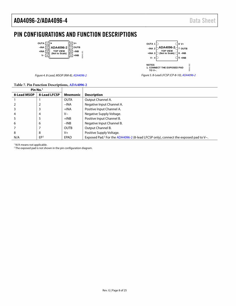
PIN CONFIGURATIONS AND FUNCTION DESCRIPTIONS OUTA 1
–INA 2
+INA 3
V– 4
V+8
OUTB7
–INB6
+INB5
ADA4096-2TOP VIEW
(Not to Scale)
0924
1-20
1
Figure 4. 8-Lead, MSOP (RM-8), ADA4096-2
V+
OUTB
–INB
+INB
ADA4096-2TOP VIEW
(Not to Scale)3+INA
4V–
1OUTA
2–INA
6
5
8
7
NOTES1. CONNECT THE EXPOSED PAD
TO V–. 0924
1-20
2
Figure 5. 8-Lead LFCSP (CP-8-10), ADA4096-2
Table 7. Pin Function Descriptions, ADA4096-2 Pin No.1
Mnemonic Description 8-Lead MSOP 8-Lead LFCSP 1 1 OUTA Output Channel A. 2 2 −INA Negative Input Channel A. 3 3 +INA Positive Input Channel A. 4 4 V− Negative Supply Voltage. 5 5 +INB Positive Input Channel B. 6 6 −INB Negative Input Channel B. 7 7 OUTB Output Channel B. 8 8 V+ Positive Supply Voltage. N/A EP2 EPAD Exposed Pad.2 For the ADA4096-2 (8-lead LFCSP only), connect the exposed pad to V−. 1 N/A means not applicable. 2 The exposed pad is not shown in the pin configuration diagram.
Data Sheet ADA4096-2/ADA4096-4
Rev. G | Page 9 of 25
0924
1-10
1
ADA4096-4
1
2
3
4
5
6
7
–INA
+INA
V+
OUTB
–INB
+INB
OUTA 14
13
12
11
10
9
8
–IND
+IND
V–
OUTC
–INC
+INC
OUTD
TOP VIEW(Not to Scale)
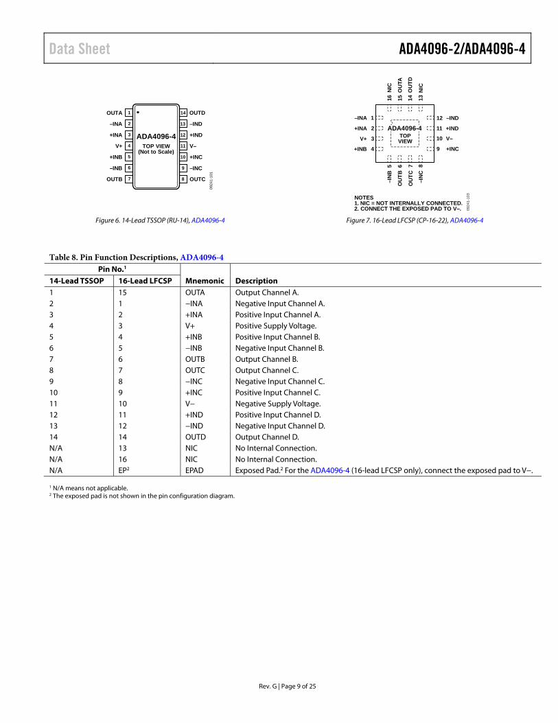
Figure 6. 14-Lead TSSOP (RU-14), ADA4096-4
0924
1-10
3
12
11
10
1
3
4
–IND
+IND
V–
9 +INC
–INA
V+
2+INA
+INB
6O
UTB
5–I
NB
7O
UTC
8–I
NC
16N
IC
15O
UTA
14O
UTD
13N
IC
TOPVIEW
ADA4096-4
NOTES1. NIC = NOT INTERNALLY CONNECTED.2. CONNECT THE EXPOSED PAD TO V–.
Figure 7. 16-Lead LFCSP (CP-16-22), ADA4096-4
Table 8. Pin Function Descriptions, ADA4096-4 Pin No.1
Mnemonic Description 14-Lead TSSOP 16-Lead LFCSP 1 15 OUTA Output Channel A. 2 1 −INA Negative Input Channel A. 3 2 +INA Positive Input Channel A. 4 3 V+ Positive Supply Voltage. 5 4 +INB Positive Input Channel B. 6 5 −INB Negative Input Channel B. 7 6 OUTB Output Channel B. 8 7 OUTC Output Channel C. 9 8 −INC Negative Input Channel C. 10 9 +INC Positive Input Channel C. 11 10 V− Negative Supply Voltage. 12 11 +IND Positive Input Channel D. 13 12 −IND Negative Input Channel D. 14 14 OUTD Output Channel D. N/A 13 NIC No Internal Connection. N/A 16 NIC No Internal Connection. N/A EP2 EPAD Exposed Pad.2 For the ADA4096-4 (16-lead LFCSP only), connect the exposed pad to V−. 1 N/A means not applicable. 2 The exposed pad is not shown in the pin configuration diagram.
ADA4096-2/ADA4096-4 Data Sheet
Rev. G | Page 10 of 25
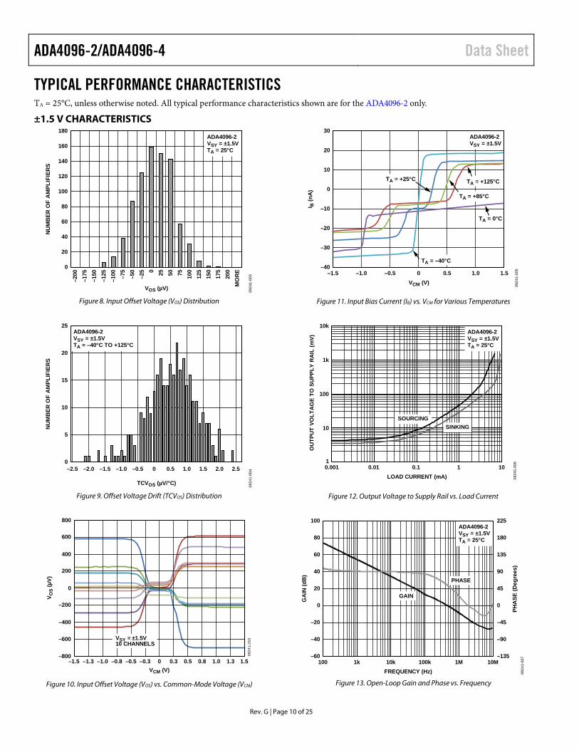
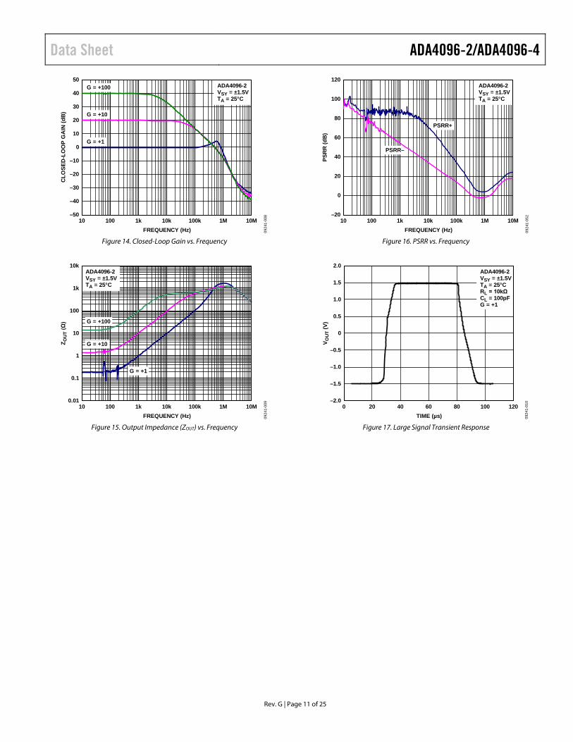
TYPICAL PERFORMANCE CHARACTERISTICS TA = 25°C, unless otherwise noted. All typical performance characteristics shown are for the ADA4096-2 only.
±1.5 V CHARACTERISTICS 180
0
20
40
60
80
100
120
140
160
–200
–175
–150
–125
–100 –7
5–5
0–2
5 0 25 50 75 100
125
150
175
200
MO
RE
NU
MB
ER O
F A
MPL
IFIE
RS
VOS (µV)
ADA4096-2VSY = ±1.5VTA = 25°C
0924
1-00
3
Figure 8. Input Offset Voltage (VOS) Distribution
25
20
15
10
5
0–2.5 –2.0 –1.5 –1.0 –0.5 0 0.5 1.0 1.5 2.0 2.5
NU
MB
ER O
F A
MPL
IFIE
RS
TCVOS (µV/°C)
ADA4096-2VSY = ±1.5VTA = –40°C TO +125°C
0924
1-00
4
Figure 9. Offset Voltage Drift (TCVOS) Distribution
800
400
0
–400
–800–1.5 1.5
0924
1-21
0
V OS
(µV)
VCM (V)
–200
–600
200
600
1.31.00.8–1.3 –1.0 0.50.30–0.3–0.5–0.8
VSY = ±1.5V10 CHANNELS
Figure 10. Input Offset Voltage (VOS) vs. Common-Mode Voltage (VCM)
30
–1.5 –1.0 –0.5 0 0.5 1.0 1.5–40
–30
–20
–10
0
10
20
I B (n
A)
VCM (V)
ADA4096-2VSY = ±1.5V
TA = 0°C
TA = +25°C
TA = +85°C
TA = +125°C
TA = –40°C
0924
1-00
5
Figure 11. Input Bias Current (IB) vs. VCM for Various Temperatures
10k
1k
100
0.001 0.01 0.1 1 10
10
1
LOAD CURRENT (mA)
ADA4096-2VSY = ±1.5VTA = 25°C
SOURCINGSINKING
0924
1-00
6
OU
TPU
T VO
LTA
GE
TO S
UPP
LY R
AIL
(mV)
Figure 12. Output Voltage to Supply Rail vs. Load Current
100
80
60
40
20
0
–20
–40
100 1k 10k 100k 1M 10M–60
GA
IN (d
B)
PHA
SE (D
egre
es)
FREQUENCY (Hz)
ADA4096-2VSY = ±1.5VTA = 25°C
GAIN
PHASE
0924
1-00
7–135
–90
–45
0
45
90
135
180
225
Figure 13. Open-Loop Gain and Phase vs. Frequency
Data Sheet ADA4096-2/ADA4096-4
Rev. G | Page 11 of 25
50
40
30
20
10
0
–10
–20
–30
–40
10 100 1k 10k 100k 1M 10M–50
CLO
SED
-LO
OP
GA
IN (d
B)
FREQUENCY (Hz)
ADA4096-2VSY = ±1.5VTA = 25°C
G = +100
G = +10
G = +1
0924
1-00
8
Figure 14. Closed-Loop Gain vs. Frequency
10k
1k
100
10
1
0.1
10 100 1k 10k 100k 1M 10M0.01
Z OU
T (Ω
)
FREQUENCY (Hz)
ADA4096-2VSY = ±1.5VTA = 25°C
G = +100
G = +10
G = +1
0924
1-00
9
Figure 15. Output Impedance (ZOUT) vs. Frequency
120
100
80
60
40
20
0
10 100 1k 10k 100k 1M 10M–20
PSR
R (d
B)
FREQUENCY (Hz)
ADA4096-2VSY = ±1.5VTA = 25°C
PSRR–
PSRR+
0924
1-05
2
Figure 16. PSRR vs. Frequency
2.0
0 20 40 60 80 100 120–2.0
–1.5
–1.0
–0.5
0
0.5
1.0
1.5
V OU
T (V
)
TIME (µs)
ADA4096-2VSY = ±1.5VTA = 25°CRL = 10kΩCL = 100pFG = +1
0924
1-01
0
Figure 17. Large Signal Transient Response
ADA4096-2/ADA4096-4 Data Sheet
Rev. G | Page 12 of 25
0.08
0 5 10 15 20 25 30–0.10
–0.08
–0.06
–0.02
–0.04
0
0.02
0.04
0.06
V OU
T (V
)
TIME (µs)
ADA4096-2VSY = ±1.5VTA = 25°CRL = 10kΩCL = 100pFG = +1
0924
1-01
1
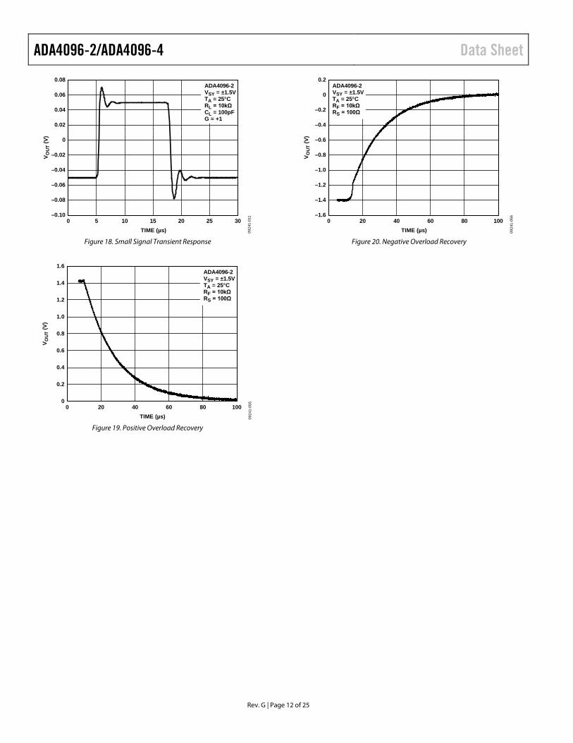
Figure 18. Small Signal Transient Response
1.6
1.4
1.2
1.0
0.8
0.6
0.4
0.2
0 20 40 60 80 1000
V OU
T (V
)
TIME (µs)
ADA4096-2VSY = ±1.5VTA = 25°CRF = 10kΩRS = 100Ω
0924
1-05
5
Figure 19. Positive Overload Recovery
0.2
0 20 40 60 80 100–1.6
–1.4
–1.2
–1.0
–0.8
–0.6
–0.4
–0.2
0
V OU
T (V
)
TIME (µs)
ADA4096-2VSY = ±1.5VTA = 25°CRF = 10kΩRS = 100Ω
0924
1-05
6
Figure 20. Negative Overload Recovery
Data Sheet ADA4096-2/ADA4096-4
Rev. G | Page 13 of 25
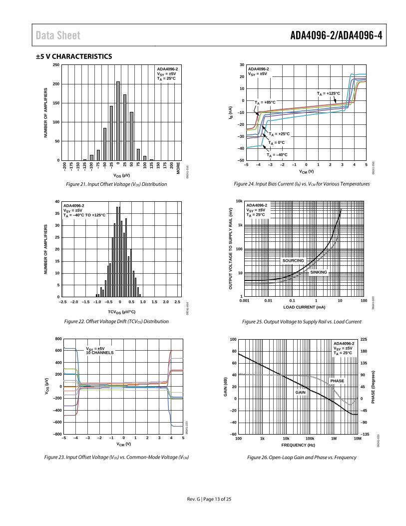
±5 V CHARACTERISTICS 250
200
150
100
50
0
–200
–175
–150
–125
–100 –7
5–5
0–2
5 0 25 50 75 100
125
150
175
200
MO
RE
NU
MB
ER O
F A
MPL
IFIE
RS
VOS (µV)
ADA4096-2VSY = ±5VTA = 25°C
0924
1-01
5
Figure 21. Input Offset Voltage (VOS) Distribution
40
20
25
30
35
15
10
5
0–2.5 –2.0 –1.5 –1.0 –0.5 0 0.5 1.0 1.5 2.0 2.5
NU
MB
ER O
F A
MPL
IFIE
RS
TCVOS (µV/°C)
ADA4096-2VSY = ±5VTA = –40°C TO +125°C
0924
1-01
6
Figure 22. Offset Voltage Drift (TCVOS) Distribution
800
400
0
–400
–800–5 5
0924
1-22
3
V OS
(µV)
VCM (V)
–200
–600
200
600
432–4 –3 10–1–2
VSY = ±5V10 CHANNELS
Figure 23. Input Offset Voltage (VOS) vs. Common-Mode Voltage (VCM)
30
–5 –4 –3 –2 –1 0 1 2 3 4 5–50
–40
–30
–20
–10
0
10
20
I B (n
A)
VCM (V)
ADA4096-2VSY = ±5V
TA = 0°C
TA = +25°C
TA = +85°C
TA = +125°C
TA = –40°C
0924
1-05
0
Figure 24. Input Bias Current (IB) vs. VCM for Various Temperatures
10k
1k
100
0.001 0.01 0.1 1 10 100
10
1
LOAD CURRENT (mA)
ADA4096-2VSY = ±5VTA = 25°C
SOURCING
SINKING
0924
1-02
3
OU
TPU
T VO
LTA
GE
TO S
UPP
LY R
AIL
(mV)
Figure 25. Output Voltage to Supply Rail vs. Load Current
100
80
60
40
20
0
–20
–40
100 1k 10k 100k 1M 10M–60
GA
IN (d
B)
PHA
SE (D
egre
es)
FREQUENCY (Hz)
ADA4096-2VSY = ±5VTA = 25°C
GAIN
PHASE09
241-
020–135
–90
–45
0
45
90
135
180
225
Figure 26. Open-Loop Gain and Phase vs. Frequency
ADA4096-2/ADA4096-4 Data Sheet
Rev. G | Page 14 of 25
50
40
30
20
10
0
–10
–20
–30
–40
10 100 1k 10k 100k 1M 10M–50
CLO
SED
-LO
OP
GA
IN (d
B)
FREQUENCY (Hz)
ADA4096-2VSY = ±5VTA = 25°C
G = +100
G = +10
G = +1
0924
1-02
4
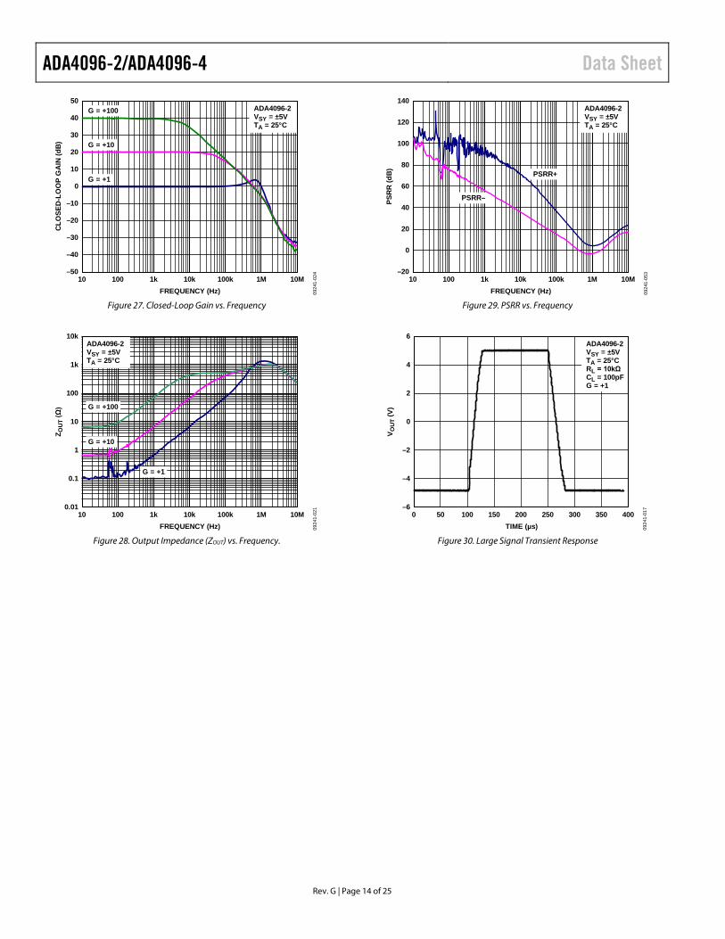
Figure 27. Closed-Loop Gain vs. Frequency
10k
1k
100
10
1
0.1
10 100 1k 10k 100k 1M 10M0.01
Z OUT
(Ω)
FREQUENCY (Hz)
ADA4096-2VSY = ±5VTA = 25°C
G = +100
G = +10
G = +1
0924
1-02
1
Figure 28. Output Impedance (ZOUT) vs. Frequency.
140
120
100
80
60
40
20
0
10 100 1k 10k 100k 1M 10M–20
PSR
R (d
B)
FREQUENCY (Hz)
ADA4096-2VSY = ±5VTA = 25°C
PSRR–
PSRR+
0924
1-05
3
Figure 29. PSRR vs. Frequency
6
0 50 100 150 200 250 300 350 400–6
–4
–2
0
2
4
V OU
T (V
)
TIME (µs)
ADA4096-2VSY = ±5VTA = 25°CRL = 10kΩCL = 100pFG = +1
0924
1-01
7
Figure 30. Large Signal Transient Response
Data Sheet ADA4096-2/ADA4096-4
Rev. G | Page 15 of 25
0.08
0 5 10 15 20 25 30–0.10
–0.08
–0.06
–0.02
–0.04
0
0.02
0.04
0.06
V OU
T (V
)
TIME (µs)
ADA4096-2VSY = ±5VTA = 25°CRL = 10kΩCL = 100pFG = +1
0924
1-01
8
Figure 31. Small Signal Transient Response
6
5
4
3
2
1
0 20 40 60 80 1000
V OU
T (V
)
TIME (µs)
ADA4096-2VSY = ±5VTA = 25°CRF = 10kΩRS = 100Ω
0924
1-05
7
Figure 32. Positive Overload Recovery
1
0
–1
–2
–3
–4
0 20 40 60 80 100–5
V OU
T (V
)
TIME (µs)
ADA4096-2VSY = ±5VTA = 25°CRF = 10kΩRS = 100Ω
0924
1-05
8
Figure 33. Negative Overload Recovery
ADA4096-2/ADA4096-4 Data Sheet
Rev. G | Page 16 of 25
±15 V CHARACTERISTICS 250
200
150
100
50
0
–200
–175
–150
–125
–100 –7
5–5
0–2
5 0 25 50 75 100
125
150
175
200
MO
RE
NU
MB
ER O
F A
MPL
IFIE
RS
VOS (µV)
ADA4096-2VSY = ±15VTA = 25°C
0924
1-02
7
Figure 34. Input Offset Voltage (VOS) Distribution
35
20
25
30
15
10
5
0–2.5 –2.0 –1.5 –1.0 –0.5 0 0.5 1.0 1.5 2.0 2.5
NU
MB
ER O
F A
MPL
IFIE
RS
TCVOS (µV/°C)
ADA4096-2VSY = ±15VTA = –40°C TO +125°C
0924
1-02
8
Figure 35. Offset Voltage Drift (TCVOS) Distribution
800
400
0
–400
–800–15 15
0924
1-23
6
V OS
(µV)
VCM (V)
–200
–600
200
600
1296–12 –9 30–3–6
VSY = ±15V10 CHANNELS
Figure 36. Input Offset Voltage (VOS) vs. Common-Mode Voltage (VCM)
40
30
–15 –10 –5 0 5 10 15–60
–50
–40
–30
–20
–10
0
10
20
I B (n
A)
VCM (V)
ADA4096-2VSY = ±15V
TA = 0°CTA = +25°C
TA = +85°CTA = +125°C
TA = –40°C
0924
1-05
1
Figure 37. Input Bias Current (IB) vs. VCM for Various Temperatures
10k
1k
100
0.001 0.01 0.1 1 10 100
10
1
LOAD CURRENT (mA)
ADA4096-2VSY = ±15VTA = 25°C
SOURCING
SINKING
0924
1-03
4
OU
TPU
T VO
LTA
GE
TO S
UPP
LY R
AIL
(mV)
Figure 38. Output Voltage to Supply Rail vs. Load Current
100
80
60
40
20
0
–20
–40
100 1k 10k 100k 1M 10M–60
GA
IN (d
B)
PHA
SE (D
egre
es)
FREQUENCY (Hz)
ADA4096-2VSY = ±15VTA = 25°C
GAIN
PHASE
0924
1-03
0–135
–90
–45
0
45
90
135
180
225
Figure 39. Open-Loop Gain and Phase vs. Frequency
Data Sheet ADA4096-2/ADA4096-4
Rev. G | Page 17 of 25
50
40
30
20
10
0
–10
–20
–30
10 100 1k 10k 100k 1M 10M–40
CLO
SED
-LO
OP
GA
IN (d
B)
FREQUENCY (Hz)
ADA4096-2VSY = ±15VTA = 25°C
G = +100
G = +10
G = +1
0924
1-03
6
Figure 40. Closed-Loop Gain vs. Frequency
10k
1k
100
10
1
0.1
10 100 1k 10k 100k 1M 10M0.01
Z OU
T (Ω
)
FREQUENCY (Hz)
ADA4096-2VSY = ±15VTA = 25°C
G = +100
G = +10
G = +1
0924
1-03
5
Figure 41. Output Impedance (ZOUT) vs. Frequency
120
100
80
60
40
20
0
10 100 1k 10k 100k 1M 10M–20
PSR
R (d
B)
FREQUENCY (Hz)
ADA4096-2VSY = ±15VTA = 25°C
PSRR–
PSRR+
0924
1-05
4
Figure 42. PSRR vs. Frequency
15
0 50 100 150 200 250 300 350 400–15
–10
–5
0
5
10
V OU
T (V
)
TIME (µs)
ADA4096-2VSY = ±15VTA = 25°CRL = 10kΩCL = 100pFG = +1
0924
1-03
1
Figure 43. Large Signal Transient Response
ADA4096-2/ADA4096-4 Data Sheet
Rev. G | Page 18 of 25
0.08
0 5 10 15 20 25 30–0.10
–0.08
–0.06
–0.02
–0.04
0
0.02
0.04
0.06
V OU
T (V
)
TIME (µs)
ADA4096-2VSY = ±15VTA = 25°CRL = 10kΩCL = 100pFG = +1
0924
1-03
2
Figure 44. Small Signal Transient Response
16
12
14
10
8
6
4
2
0 20 40 60 80 1000
V OU
T (V
)
TIME (µs)
ADA4096-2VSY = ±15VTA = 25°CRF = 10kΩRS = 100Ω
0924
1-05
9
Figure 45. Positive Overload Recovery
0
–4
–2
–6
–8
–10
–12
–14
0 20 40 60 80 100–16
V OU
T (V
)
TIME (µs)
ADA4096-2VSY = ±15VTA = 25°CRF = 10kΩRS = 100Ω
0924
1-06
0
Figure 46. Negative Overload Recovery
Data Sheet ADA4096-2/ADA4096-4
Rev. G | Page 19 of 25
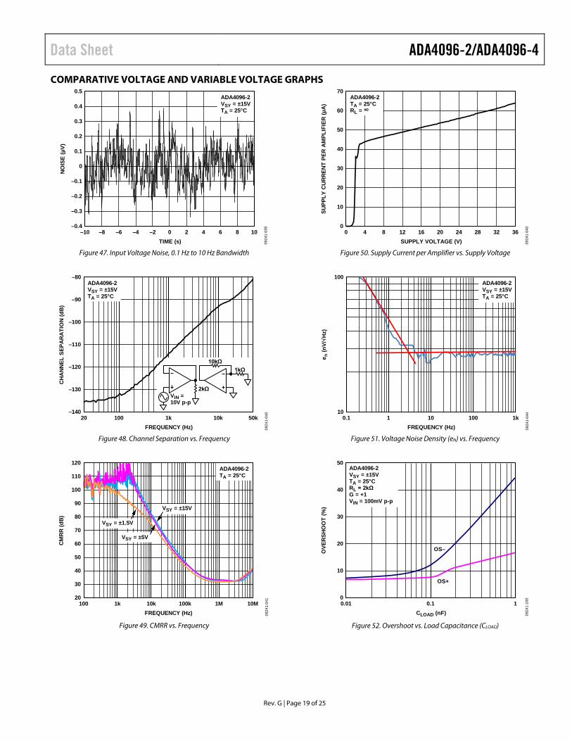
COMPARATIVE VOLTAGE AND VARIABLE VOLTAGE GRAPHS 0.5
0.4
0.3
0.2
0.1
0
–0.1
–0.2
–0.3
–10 –8 –6 –4 –2 0 2 4 6 8 10–0.4
NO
ISE
(µV)
TIME (s)
ADA4096-2VSY = ±15VTA = 25°C
0924
1-03
9
Figure 47. Input Voltage Noise, 0.1 Hz to 10 Hz Bandwidth
–80
20 100 1k 10k 50k–140
–130
–120
–110
–100
–90
CH
AN
NEL
SEP
AR
ATI
ON
(dB
)
FREQUENCY (Hz)
ADA4096-2VSY = ±15VTA = 25°C
0924
1-04
0
2kΩ
10kΩ1kΩ
VIN =10V p-p
Figure 48. Channel Separation vs. Frequency
120
110
100
90
80
70
60
50
40
30
100 1k 10k 100k 1M 10M20
CM
RR
(dB
)
FREQUENCY (Hz)
ADA4096-2TA = 25°C
VSY = ±15V
VSY = ±1.5V
VSY = ±5V
0924
1-04
1
Figure 49. CMRR vs. Frequency
70
60
50
40
30
20
10
0 36322824201612840
SUPP
LY C
UR
REN
T PE
R A
MPL
IFIE
R (µ
A)
SUPPLY VOLTAGE (V)
ADA4096-2TA = 25°CRL = ∞
0924
1-04
3
Figure 50. Supply Current per Amplifier vs. Supply Voltage
100
0.1 1k10010110
e n (n
V/ H
z)
FREQUENCY (Hz)
ADA4096-2VSY = ±15VTA = 25°C
0924
1-04
4
Figure 51. Voltage Noise Density (eN) vs. Frequency
50
0.01 10.10
10
20
30
40
OVE
RSH
OO
T (%
)
CLOAD (nF)
ADA4096-2VSY = ±15VTA = 25°CRL = 2kΩG = +1VIN = 100mV p-p
0924
1-10
0
OS–
OS+
Figure 52. Overshoot vs. Load Capacitance (CLOAD)
ADA4096-2/ADA4096-4 Data Sheet
Rev. G | Page 20 of 25
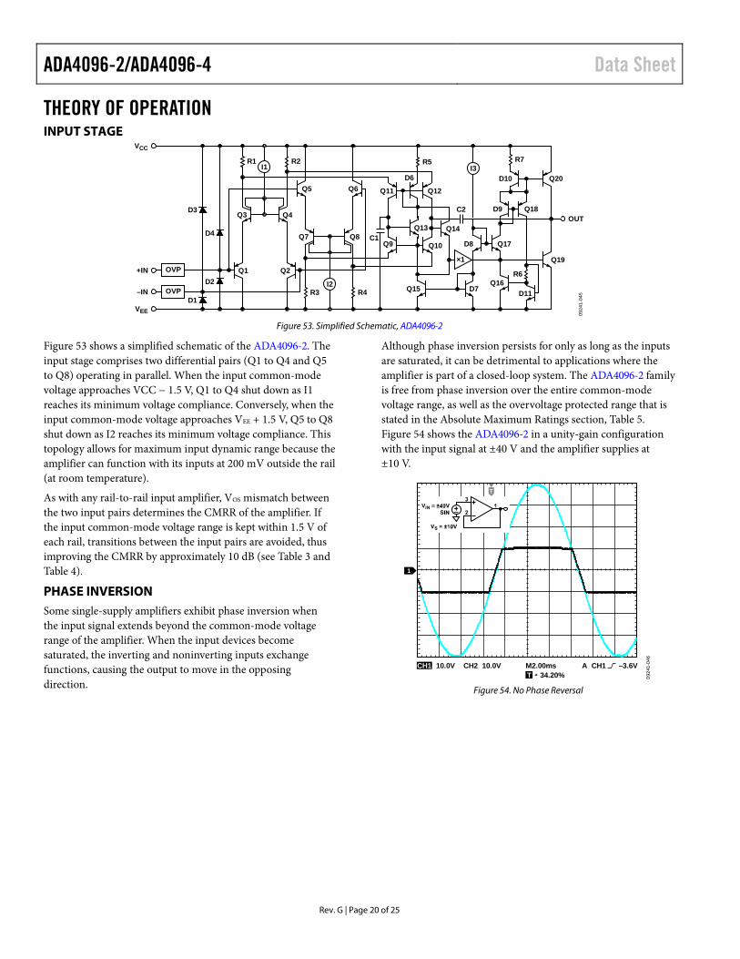
THEORY OF OPERATION INPUT STAGE
0924
1-04
5
R6
VCC
+IN
–IN
VEE
OVP
OVP
OUT
R7
D10 Q20
Q19
D11Q16
D7Q15
D8
Q14
Q17Q10
Q13
Q18D9
×1
I3R2R1
R3 R4
C2
Q12
D6
R5
Q9
Q11Q6
Q8Q7
Q5
Q4Q3
Q1 Q2
I2
I1
C1
D3
D1
D4
D2
Figure 53. Simplified Schematic, ADA4096-2
Figure 53 shows a simplified schematic of the ADA4096-2. The input stage comprises two differential pairs (Q1 to Q4 and Q5 to Q8) operating in parallel. When the input common-mode voltage approaches VCC − 1.5 V, Q1 to Q4 shut down as I1 reaches its minimum voltage compliance. Conversely, when the input common-mode voltage approaches VEE + 1.5 V, Q5 to Q8 shut down as I2 reaches its minimum voltage compliance. This topology allows for maximum input dynamic range because the amplifier can function with its inputs at 200 mV outside the rail (at room temperature).
As with any rail-to-rail input amplifier, VOS mismatch between the two input pairs determines the CMRR of the amplifier. If the input common-mode voltage range is kept within 1.5 V of each rail, transitions between the input pairs are avoided, thus improving the CMRR by approximately 10 dB (see Table 3 and Table 4).
PHASE INVERSION Some single-supply amplifiers exhibit phase inversion when the input signal extends beyond the common-mode voltage range of the amplifier. When the input devices become saturated, the inverting and noninverting inputs exchange functions, causing the output to move in the opposing direction.
Although phase inversion persists for only as long as the inputs are saturated, it can be detrimental to applications where the amplifier is part of a closed-loop system. The ADA4096-2 family is free from phase inversion over the entire common-mode voltage range, as well as the overvoltage protected range that is stated in the Absolute Maximum Ratings section, Table 5. Figure 54 shows the ADA4096-2 in a unity-gain configuration with the input signal at ±40 V and the amplifier supplies at ±10 V.
CH1 10.0V CH2 10.0V M2.00ms A CH1 –3.6VT 34.20%
1
T
0924
1-04
6
Figure 54. No Phase Reversal
Data Sheet ADA4096-2/ADA4096-4
Rev. G | Page 21 of 25
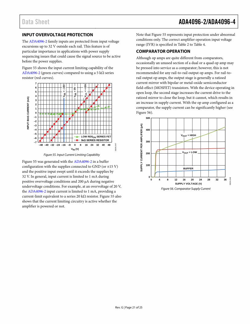
INPUT OVERVOLTAGE PROTECTION The ADA4096-2 family inputs are protected from input voltage excursions up to 32 V outside each rail. This feature is of particular importance in applications with power supply sequencing issues that could cause the signal source to be active before the power supplies.
Figure 55 shows the input current limiting capability of the ADA4096-2 (green curves) compared to using a 5 kΩ series resistor (red curves).
7
–48 –40 –32 –24 –16 –8 0 8 16 24 32 40 48–7–6–5–4–3–2–10123456
INPU
T B
IAS
CU
RR
ENT
(mA
)
VIN (V)
V EE
= –1
5V
V EE
= 0V
V CC
= +
15V
LOW RDSON SERIES FET5kΩ SERIES RESISTOR
0924
1-04
7
Figure 55. Input Current Limiting Capability
Figure 55 was generated with the ADA4096-2 in a buffer configuration with the supplies connected to GND (or ±15 V) and the positive input swept until it exceeds the supplies by 32 V. In general, input current is limited to 1 mA during positive overvoltage conditions and 200 µA during negative undervoltage conditions. For example, at an overvoltage of 20 V, the ADA4096-2 input current is limited to 1 mA, providing a current-limit equivalent to a series 20 kΩ resistor. Figure 55 also shows that the current limiting circuitry is active whether the amplifier is powered or not.
Note that Figure 55 represents input protection under abnormal conditions only. The correct amplifier operation input voltage range (IVR) is specified in Table 2 to Table 4.
COMPARATOR OPERATION Although op amps are quite different from comparators, occasionally an unused section of a dual or a quad op amp may be pressed into service as a comparator; however, this is not recommended for any rail-to-rail output op amps. For rail-to-rail output op amps, the output stage is generally a ratioed current mirror with bipolar or metal-oxide semiconductor field-effect (MOSFET) transistors. With the device operating in open loop, the second stage increases the current drive to the ratioed mirror to close the loop, but it cannot, which results in an increase in supply current. With the op amp configured as a comparator, the supply current can be significantly higher (see Figure 56).
500
400
300
200
100
0 36322824201612840
SUPP
LY C
UR
REN
T PE
R A
MPL
IFIE
R (µ
A)
SUPPLY VOLTAGE (V)
VOUT = HIGH
VOUT = LOW
BUFFER
0924
1-04
8
Figure 56. Comparator Supply Current
ADA4096-2/ADA4096-4 Data Sheet
Rev. G | Page 22 of 25
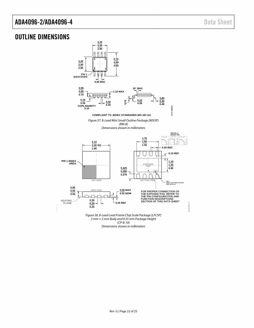
OUTLINE DIMENSIONS
COMPLIANT TO JEDEC STANDARDS MO-187-AA
6°0°
0.800.550.40
4
8
1
5
0.65 BSC
0.400.25
1.10 MAX
3.203.002.80
COPLANARITY0.10
0.230.09
3.203.002.80
5.154.904.65
PIN 1IDENTIFIER
15° MAX0.950.850.75
0.150.05
10-0
7-20
09-B
Figure 57. 8-Lead Mini Small Outline Package [MSOP]
(RM-8) Dimensions shown in millimeters
1.701.601.50
0.4250.3500.275
8
1
5
4
0.300.250.20
PIN 1 INDEXAREA
0.600.550.50
1.101.000.90
0.20 REF
0.15 REF
0.05 MAX0.02 NOM
0.50 BSC
2.102.00 SQ1.90
PKG
-003
580
02-0
8-20
17-C
SEATINGPLANE
TOP VIEW
SIDE VIEW
EXPOSEDPAD
BOTTOM VIEW
FOR PROPER CONNECTION OFTHE EXPOSED PAD, REFER TOTHE PIN CONFIGURATION ANDFUNCTION DESCRIPTIONSSECTION OF THIS DATA SHEET
PIN 1INDIC ATOR AREA OPTIONS(SEE DETAIL A)
1
DETAIL A(JEDEC 95)
Figure 58. 8-Lead Lead Frame Chip Scale Package [LFCSP]
2 mm × 2 mm Body and 0.55 mm Package Height (CP-8-10)
Dimensions shown in millimeters
Data Sheet ADA4096-2/ADA4096-4
Rev. G | Page 23 of 25
COMPLIANT TO JEDEC STANDARDS MO-153-AB-1 0619
08-A
8°0°
4.504.404.30
14 8
71
6.40BSC
PIN 1
5.105.004.90
0.65 BSC
0.150.05 0.30
0.19
1.20MAX
1.051.000.80
0.200.09 0.75
0.600.45
COPLANARITY0.10
SEATINGPLANE
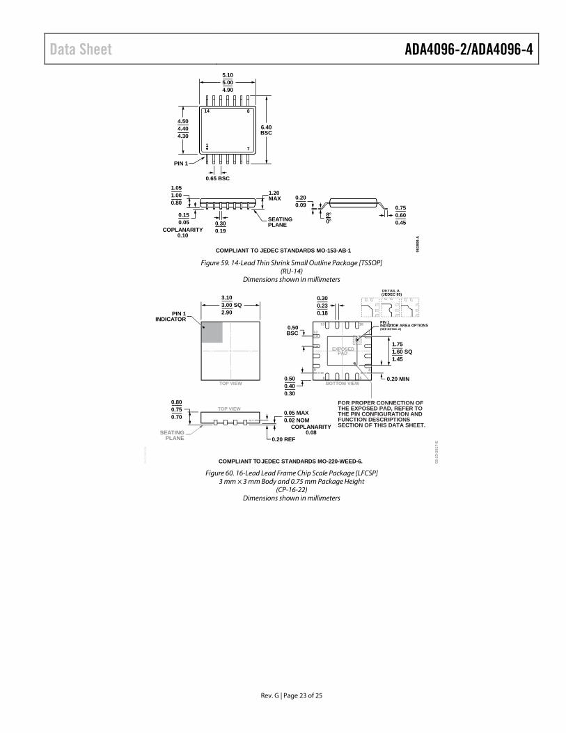
Figure 59. 14-Lead Thin Shrink Small Outline Package [TSSOP]
(RU-14) Dimensions shown in millimeters
0.300.230.18
1.751.60 SQ1.45
3.103.00 SQ2.90
10.50BSC
BOTTOM VIEWTOP VIEW
16
58
9
12
13
4
0.500.400.30
0.05 MAX0.02 NOM
0.20 REF
0.20 MIN
COPLANARITY0.08
PIN 1INDICATOR
0.800.750.70
COMPLIANT TOJEDEC STANDARDS MO-220-WEED-6.PKG
-005
138
SEATINGPLANE
TOP VIEW
EXPOSEDPAD
02-2
3-20
17-E
PIN 1INDICATOR AREA OPTIONS(SEE DETAIL A)
DETAIL A(JEDEC 95)
FOR PROPER CONNECTION OFTHE EXPOSED PAD, REFER TOTHE PIN CONFIGURATION ANDFUNCTION DESCRIPTIONSSECTION OF THIS DATA SHEET.
Figure 60. 16-Lead Lead Frame Chip Scale Package [LFCSP]
3 mm × 3 mm Body and 0.75 mm Package Height (CP-16-22)
Dimensions shown in millimeters
ADA4096-2/ADA4096-4 Data Sheet
Rev. G | Page 24 of 25
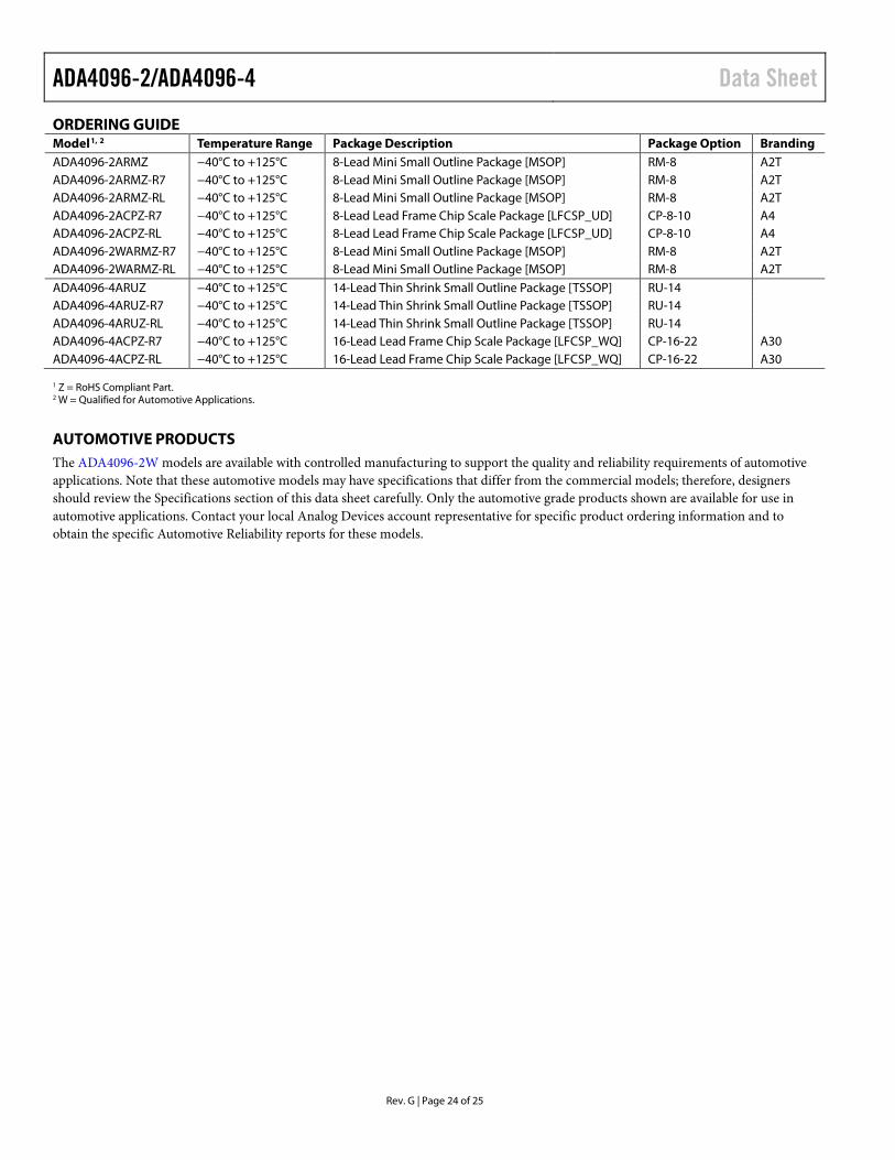
ORDERING GUIDE Model1, 2 Temperature Range Package Description Package Option Branding ADA4096-2ARMZ −40°C to +125°C 8-Lead Mini Small Outline Package [MSOP] RM-8 A2T ADA4096-2ARMZ-R7 −40°C to +125°C 8-Lead Mini Small Outline Package [MSOP] RM-8 A2T ADA4096-2ARMZ-RL −40°C to +125°C 8-Lead Mini Small Outline Package [MSOP] RM-8 A2T ADA4096-2ACPZ-R7 −40°C to +125°C 8-Lead Lead Frame Chip Scale Package [LFCSP_UD] CP-8-10 A4 ADA4096-2ACPZ-RL −40°C to +125°C 8-Lead Lead Frame Chip Scale Package [LFCSP_UD] CP-8-10 A4 ADA4096-2WARMZ-R7 −40°C to +125°C 8-Lead Mini Small Outline Package [MSOP] RM-8 A2T ADA4096-2WARMZ-RL −40°C to +125°C 8-Lead Mini Small Outline Package [MSOP] RM-8 A2T ADA4096-4ARUZ −40°C to +125°C 14-Lead Thin Shrink Small Outline Package [TSSOP] RU-14 ADA4096-4ARUZ-R7 −40°C to +125°C 14-Lead Thin Shrink Small Outline Package [TSSOP] RU-14 ADA4096-4ARUZ-RL −40°C to +125°C 14-Lead Thin Shrink Small Outline Package [TSSOP] RU-14 ADA4096-4ACPZ-R7 −40°C to +125°C 16-Lead Lead Frame Chip Scale Package [LFCSP_WQ] CP-16-22 A30 ADA4096-4ACPZ-RL −40°C to +125°C 16-Lead Lead Frame Chip Scale Package [LFCSP_WQ] CP-16-22 A30 1 Z = RoHS Compliant Part. 2 W = Qualified for Automotive Applications.
AUTOMOTIVE PRODUCTS The ADA4096-2W models are available with controlled manufacturing to support the quality and reliability requirements of automotive applications. Note that these automotive models may have specifications that differ from the commercial models; therefore, designers should review the Specifications section of this data sheet carefully. Only the automotive grade products shown are available for use in automotive applications. Contact your local Analog Devices account representative for specific product ordering information and to obtain the specific Automotive Reliability reports for these models.

Data Sheet ADA4096-2/ADA4096-4
Rev. G | Page 25 of 25
NOTES
©2011–2017 Analog Devices, Inc. All rights reserved. Trademarks and registered trademarks are the property of their respective owners. D09241-0-9/17(G)