Embed Size (px)
Citation preview
PRODUCTS AND SPECIFICATIONS DISCUSSED HEREIN ARE SUBJECT TO CHANGE BY MICRON WITHOUT NOTICE.
109005aef8091e6a8 Micron Technology, Inc., reserves the right to change products or specifications without notice.256MSDRAM_G.p65 – Rev. G; Pub. 9/03 ©2003 Micron Technology, Inc.
256Mb: x4, x8, x16SDRAM
Table 2: Key Timing Parameters
SPEED CLOCK ACCESS TIME SETUP HOLDGRADE FREQUENCY CL = 2* CL = 3* TIME TIME
-7E 143 MHz – 5.4ns 1.5ns 0.8ns-75 133 MHz – 5.4ns 1.5ns 0.8ns-7E 133 MHz 5.4ns – 1.5ns 0.8ns-75 100 MHz 6ns – 1.5ns 0.8ns
64 Meg x 4 32 Meg x 8 16 Meg x 16Configuration 16 Meg x 4 x 4 banks 8 Meg x 8 x 4 banks 4 Meg x 16 x 4 banks
Refresh Count 8K 8K 8K
Row Addressing 8K (A0–A12) 8K (A0–A12) 8K (A0–A12)
Bank Addressing 4 (BA0, BA1) 4 (BA0, BA1) 4 (BA0, BA1)
Column Addressing 2K (A0–A9, A11) 1K (A0–A9) 512 (A0–A8)
SYNCHRONOUSDRAM
MT48LC64M4A2 – 16 Meg x 4 x 4 banksMT48LC32M8A2 – 8 Meg x 8 x 4 banksMT48LC16M16A2 – 4 Meg x 16 x 4 banksFor the latest data sheet, please refer to the Micron Web site:www.micron.com/dramds
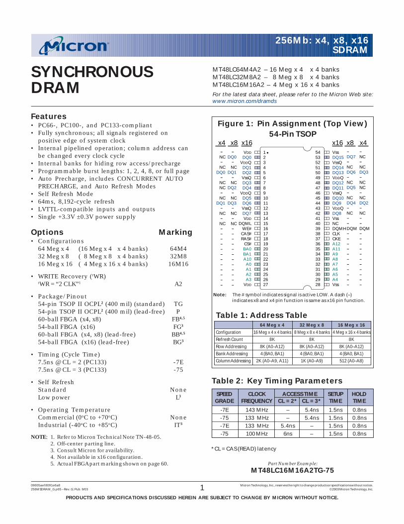
Figure 1: Pin Assignment (Top View)54-Pin TSOP
Features• PC66-, PC100-, and PC133-compliant• Fully synchronous; all signals registered on
positive edge of system clock• Internal pipelined operation; column address can
be changed every clock cycle• Internal banks for hiding row access/precharge• Programmable burst lengths: 1, 2, 4, 8, or full page• Auto Precharge, includes CONCURRENT AUTO
PRECHARGE, and Auto Refresh Modes• Self Refresh Mode• 64ms, 8,192-cycle refresh• LVTTL-compatible inputs and outputs• Single +3.3V ±0.3V power supply
Options Marking• Configurations
64 Meg x 4 (16 Meg x 4 x 4 banks) 64M432 Meg x 8 ( 8 Meg x 8 x 4 banks) 32M816 Meg x 16 ( 4 Meg x 16 x 4 banks) 16M16
• WRITE Recovery (tWR)tWR = “2 CLK”1 A2
• Package/Pinout54-pin TSOP II OCPL2 (400 mil) (standard) TG54-pin TSOP II OCPL2 (400 mil) (lead-free) P60-ball FBGA (x4, x8) FB4, 5
54-ball FBGA (x16) FG3
60-ball FBGA (x4, x8) (lead-free) BB4, 5
54-ball FBGA (x16) (lead-free) BG3
• Timing (Cycle Time)7.5ns @ CL = 2 (PC133) -7E7.5ns @ CL = 3 (PC133) -75
• Self RefreshStandard NoneLow power L3
• Operating TemperatureCommercial (0oC to +70oC) NoneIndustrial (-40oC to +85oC) IT3
NOTE: 1. Refer to Micron Technical Note TN-48-05.2. Off-center parting line.3. Consult Micron for availability.4. Not available in x16 configuration.5. Actual FBGA part marking shown on page 60.
Note: The # symbol indicates signal is active LOW. A dash (–)indicates x8 and x4 pin function is same as x16 pin function.
VDD
DQ0VDDQDQ1DQ2VssQDQ3DQ4
VDDQDQ5DQ6VssQDQ7VDD
DQMLWE#CAS#RAS#
CS#BA0BA1A10
A0A1A2A3
VDD
123456789101112131415161718192021222324252627
545352515049484746454443424140393837363534333231302928
VssDQ15VssQDQ14DQ13VDDQDQ12DQ11VssQDQ10DQ9VDDQDQ8VssNCDQMHCLKCKEA12A11A9A8A7A6A5A4Vss
x8x16 x16x8 x4x4-
DQ0- NC
DQ1- NC
DQ2- NC
DQ3- NC- NC- - - - - - - - - - - -
- NC- NC
DQ0- NCNC- NC
DQ1- NC- NC- - - - - - - - - - - -
- DQ7- NCDQ6- NCDQ5- NCDQ4- NC- - DQM- - - - - - - - - - -
- NC- NCDQ3- NCNC- NCDQ2- NC- - DQM- - - - - - - - - - -
*CL = CAS (READ) latency
Part Number Example:
MT48LC16M16A2TG-75
Table 1: Address Table
2256Mb: x4, x8, x16 SDRAM Micron Technology, Inc., reserves the right to change products or specifications without notice.256MSDRAM_G.p65 – Rev. G; Pub. 9/03 ©2003, Micron Technology, Inc.
256Mb: x4, x8, x16SDRAM
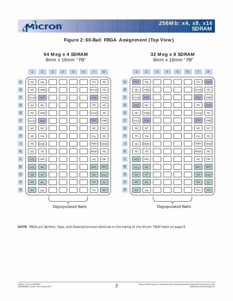
Figure 2: 60-Ball FBGA Assignment (Top View)
64 Meg x 4 SDRAM8mm x 16mm “FB”
32 Meg x 8 SDRAM 8mm x 16mm “FB”
NOTE: FBGA pin Symbol, Type, and Descriptions are identical to the listing of the 54-pin TSOP table on page 9.
A
B
C
D
E
F
G
H
J
K
L
M
N
P
R
1 2 3 4 5 6 7 8
Depopulated Balls
NC Vss
NC VssQ
VDDQ DQ3
NC NC
NC VssQ
VDDQ DQ2
NC NC
NC Vss
NC DQM
NC CK
A12 CKE
A11 A9
A8 A7
A6 A5
A4 Vss
VDD NC
VDDQ NC
DQ0 VssQ
NC NC
VDDQ NC
DQ1 VssQ
NC NC
VDD NC
WE# CAS#
RAS# NC
NC CS#
BA1 BA0
A0 A10
A2 A1
VDD A3
A
B
C
D
E
F
G
H
J
K
L
M
N
P
R
1 2 3 4 5 6 7 8
Depopulated Balls
DQ7 Vss
NC VssQ
VDDQ DQ6
DQ5 NC
NC VssQ
VDDQ DQ4
NC NC
NC Vss
NC DQM
NC CK
A12 CKE
A11 A9
A8 A7
A6 A5
A4 Vss
VDD DQ0
VDDQ NC
DQ1 VssQ
NC DQ2
VDDQ NC
DQ3 VssQ
NC NC
VDD NC
WE# CAS#
RAS# NC
NC CS#
BA1 BA0
A0 A10
A2 A1
VDD A3
3256Mb: x4, x8, x16 SDRAM Micron Technology, Inc., reserves the right to change products or specifications without notice.256MSDRAM_G.p65 – Rev. G; Pub. 9/03 ©2003, Micron Technology, Inc.
256Mb: x4, x8, x16SDRAM
Figure 3: 54-Ball FBGA Assignment (Top View)
16 Meg x 16 SDRAM8mm x 14mm “FG”
A
B
C
D
E
F
G
H
J
1 2 3 4 5 6 7 8 9
Depopulated Balls
Vss DQ15
DQ14 DQ13
DQ12 DQ11
DQ10 DQ9
DQ8 NC
UDQM CLK
A12 A11
A8 A7
Vss A5
VSSQ
VDDQ
VSSQ
VDDQ
Vss
CKE
A9
A6
A4
VDDQ
VssQ
VDDQ
VSSQ
VDD
CAS#
BA0
A0
A3
DQ0 VDD
DQ2 DQ1
DQ4 DQ3
DQ6 DQ5
LDQM DQ7
RAS# WE#
BA1 CS#
A1 A10
A2 VDD
4256Mb: x4, x8, x16 SDRAM Micron Technology, Inc., reserves the right to change products or specifications without notice.256MSDRAM_G.p65 – Rev. G; Pub. 9/03 ©2003, Micron Technology, Inc.
256Mb: x4, x8, x16SDRAM
General DescriptionThe 256Mb SDRAM is a high-speed CMOS,
dynamic random-access memory containing268,435,456 bits. It is internally configured as a quad-bank DRAM with a synchronous interface (all signalsare registered on the positive edge of the clock signal,CLK). Each of the x4’s 67,108,864-bit banks is orga-nized as 8,192 rows by 2,048 columns by4 bits. Each of the x8’s 67,108,864-bit banks is orga-nized as 8,192 rows by 1,024 columns by 8 bits. Each ofthe x16’s 67,108,864-bit banks is organized as 8,192rows by 512 columns by 16 bits.
Read and write accesses to the SDRAM are burstoriented; accesses start at a selected location and con-tinue for a programmed number of locations in a pro-grammed sequence. Accesses begin with the registra-tion of an ACTIVE command, which is then followed bya READ or WRITE command. The address bits regis-tered coincident with the ACTIVE command are used
PART NUMBER ARCHITECTURE PACKAGEMT48LC64M4A2TG 64 Meg x 4 54-pin TSOP IIMT48LC64M4A2P 64 Meg x 4 54-pin TSOP IIMT48LC64M4A2FB* 64 Meg x 4 60-ball FBGAMT48LC64M4A2BB* 64 Meg x 4 60-ball FBGAMT48LC32M8A2TG 32 Meg x 8 54-pin TSOP IIMT48LC32M8A2P 32 Meg x 8 54-pin TSOP IIMT48LC32M8A2FB* 32 Meg x 8 60-ball FBGAMT48LC32M8A2BB* 32 Meg x 8 60-ball FBGAMT48LC16M16A2TG 16 Meg x 16 54-pin TSOP IIMT48LC16M16A2P 16 Meg x 16 54-pin TSOP IIMT48LC16M16A2FG 16 Meg x 16 54-ball FBGAMT48LC16M16A2BG 16 Meg x 16 54-ball FBGA
*Actual FBGA part marking shown on pages 60 and61.
Table 3: 256 Mb SDRAM Part Numbers to select the bank and row to be accessed (BA0, BA1select the bank; A0–A12 select the row). The addressbits registered coincident with the READ or WRITE com-mand are used to select the starting column locationfor the burst access.
The SDRAM provides for programmable READ orWRITE burst lengths of 1, 2, 4, or 8 locations, or the fullpage, with a burst terminate option. An auto prechargefunction may be enabled to provide a self-timed rowprecharge that is initiated at the end of the burst se-quence.
The 256Mb SDRAM uses an internal pipelined ar-chitecture to achieve high-speed operation. This ar-chitecture is compatible with the 2n rule of prefetcharchitectures, but it also allows the column address tobe changed on every clock cycle to achieve a high-speed, fully random access. Precharging one bankwhile accessing one of the other three banks will hidethe precharge cycles and provide seamless, high-speed, random-access operation.
The 256Mb SDRAM is designed to operate in 3.3Vmemory systems. An auto refresh mode is provided,along with a power-saving, power-down mode. All in-puts and outputs are LVTTL-compatible.
SDRAMs offer substantial advances in DRAM oper-ating performance, including the ability to synchro-nously burst data at a high data rate with automaticcolumn-address generation, the ability to interleavebetween internal banks to hide precharge time andthe capability to randomly change column addresseson each clock cycle during a burst access.
5256Mb: x4, x8, x16 SDRAM Micron Technology, Inc., reserves the right to change products or specifications without notice.256MSDRAM_G.p65 – Rev. G; Pub. 9/03 ©2003, Micron Technology, Inc.
256Mb: x4, x8, x16SDRAM
Table of ContentsFunctional Block Diagram – 64 Meg x 4 .................... 6Functional Block Diagram – 32 Meg x 8 .................... 7Functional Block Diagram – 16 Meg x 16 .................. 8Pin Descriptions .......................................................... 10Ball Descriptions .......................................................... 10
Functional Description ............................................... 12Initialization ........................................................... 12Register Definition ................................................ 12
Mode Register ................................................... 12Burst Length ................................................ 12Burst Type ................................................... 13CAS Latency ................................................ 14Operating Mode .......................................... 14Write Burst Mode ........................................ 14
Commands ................................................................... 15Truth Table 1 (Commands and DQM Operation) .............. 15Command Inhibit .................................................. 16No Operation (NOP) .............................................. 16Load mode register ................................................ 16Active ....................................................................... 16Read ....................................................................... 16Write ....................................................................... 16Precharge ................................................................ 16Auto Precharge ....................................................... 16Burst Terminate ..................................................... 17Auto Refresh ........................................................... 17Self Refresh ............................................................. 17
Operation ..................................................................... 18Bank/Row Activation ............................................. 18Reads ....................................................................... 19Writes ....................................................................... 25Precharge ................................................................ 27Power-Down ........................................................... 27Clock Suspend ........................................................ 28Burst Read/Single Write ....................................... 28
Concurrent Auto Precharge ................................. 29Truth Table 2 (CKE) ...................................................... 31Truth Table 3 (Current State, Same Bank) ........................ 32Truth Table 4 (Current State, Different Bank) .................. 34
Absolute Maximum Ratings ....................................... 36DC Electrical Characteristics
and Operating Conditions ....................................... 36IDD Specifications and Conditions ............................. 36Capacitance .................................................................. 37Electrical Characteristics
and Recommended AC Operating Conditions ....... 37
AC Electrical Characteristics (Timing Table) ......... 38
Timing WaveformsInitialize and Load mode register ........................ 40Power-Down Mode ................................................ 41Clock Suspend Mode ............................................ 42Auto Refresh Mode ................................................ 43Self Refresh Mode .................................................. 44Reads
Read – Without Auto Precharge ..................... 45Read – With Auto Precharge ........................... 46Single Read – Without Auto Precharge ......... 47Single Read – With Auto Precharge ............... 48Alternating Bank Read Accesses .................... 49Read – Full-Page Burst .................................... 50Read – DQM Operation ................................... 51
WritesWrite – Without Auto Precharge ..................... 52Write – With Auto Precharge ........................... 53Single Write - Without Auto Precharge ......... 54Single Write - With Auto Precharge ................ 55Alternating Bank Write Accesses ................... 56Write – Full-Page Burst .................................... 57Write – DQM Operation ................................... 58
6256Mb: x4, x8, x16 SDRAM Micron Technology, Inc., reserves the right to change products or specifications without notice.256MSDRAM_G.p65 – Rev. G; Pub. 9/03 ©2003, Micron Technology, Inc.
256Mb: x4, x8, x16SDRAM
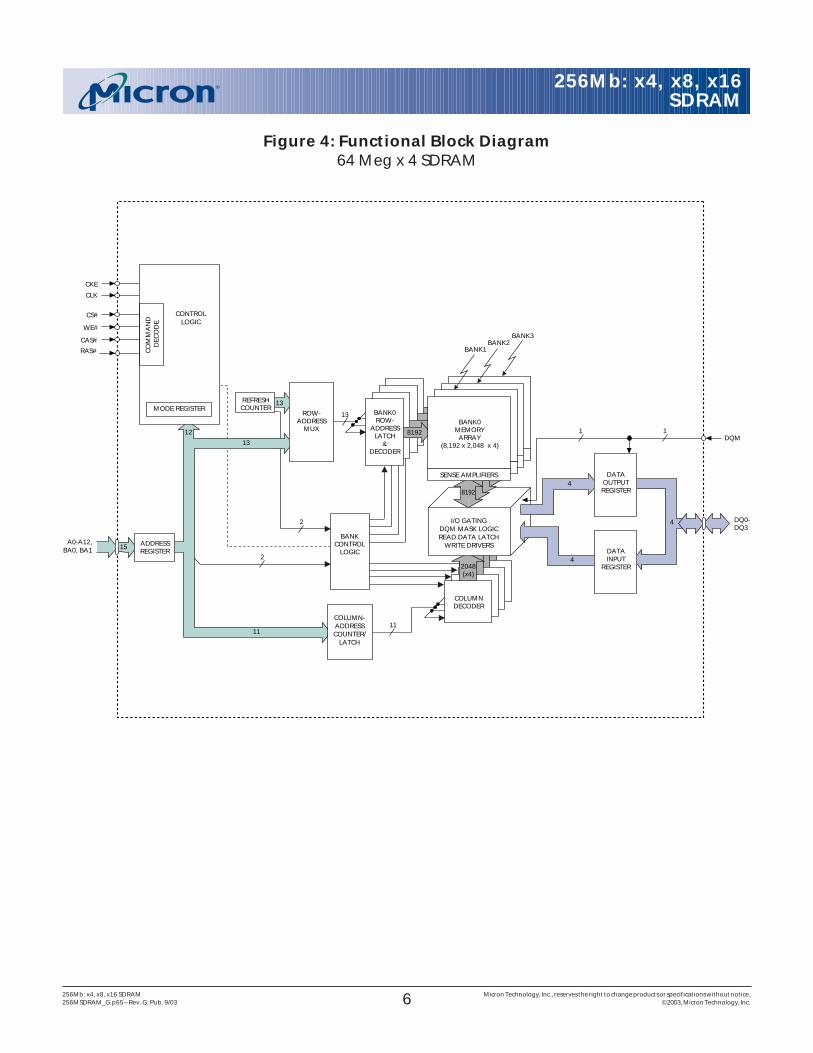
Figure 4: Functional Block Diagram64 Meg x 4 SDRAM
13
RAS#
CAS#
ROW-ADDRESS
MUX
CLK
CS#
WE#
CKE
CONTROLLOGIC
COLUMN-ADDRESSCOUNTER/
LATCH
MODE REGISTER
11
CO
MM
AN
D
DEC
OD
E
A0-A12,BA0, BA1
DQM13
ADDRESSREGISTER
15
2048(x4)
8192
I/O GATINGDQM MASK LOGICREAD DATA LATCH
WRITE DRIVERS
COLUMNDECODER
BANK0MEMORY
ARRAY(8,192 x 2,048 x 4)
BANK0ROW-
ADDRESSLATCH
&DECODER
8192
SENSE AMPLIFIERS
BANKCONTROL
LOGIC
DQ0-DQ3
4
4DATAINPUT
REGISTER
DATAOUTPUTREGISTER
4
12
BANK1BANK2
BANK3
13
11
2
1 1
2
REFRESHCOUNTER

7256Mb: x4, x8, x16 SDRAM Micron Technology, Inc., reserves the right to change products or specifications without notice.256MSDRAM_G.p65 – Rev. G; Pub. 9/03 ©2003, Micron Technology, Inc.
256Mb: x4, x8, x16SDRAM
Figure 5: Functional Block Diagram32 Meg x 8 SDRAM
13
RAS#
CAS#
ROW-ADDRESS
MUX
CLK
CS#
WE#
CKE
CONTROLLOGIC
COLUMN-ADDRESSCOUNTER/
LATCH
MODE REGISTER
10
CO
MM
AN
D
DEC
OD
E
A0-A12,BA0, BA1
DQM13
ADDRESSREGISTER
15
1024(x8)
8192
I/O GATINGDQM MASK LOGICREAD DATA LATCH
WRITE DRIVERS
COLUMNDECODER
BANK0MEMORY
ARRAY(8,192 x 1,024 x 8)
BANK0ROW-
ADDRESSLATCH
&DECODER
8192
SENSE AMPLIFIERS
BANKCONTROL
LOGIC
DQ0-DQ7
8
8DATAINPUT
REGISTER
DATAOUTPUTREGISTER
8
12
BANK1BANK2
BANK3
13
10
2
1 1
2
REFRESHCOUNTER

8256Mb: x4, x8, x16 SDRAM Micron Technology, Inc., reserves the right to change products or specifications without notice.256MSDRAM_G.p65 – Rev. G; Pub. 9/03 ©2003, Micron Technology, Inc.
256Mb: x4, x8, x16SDRAM
Figure 6: Functional Block Diagram16 Meg x 16 SDRAM
13
RAS#
CAS#
ROW-ADDRESS
MUX
CLK
CS#
WE#
CKE
CONTROLLOGIC
COLUMN-ADDRESSCOUNTER/
LATCH
MODE REGISTER
9
CO
MM
AN
D
DEC
OD
E
A0-A12,BA0, BA1
DQML,DQMH13
ADDRESSREGISTER
15
512(x16)
8192
I/O GATINGDQM MASK LOGICREAD DATA LATCH
WRITE DRIVERS
COLUMNDECODER
BANK0MEMORY
ARRAY(8,192 x 512 x 16)
BANK0ROW-
ADDRESSLATCH
&DECODER
8192
SENSE AMPLIFIERS
BANKCONTROL
LOGIC
DQ0-DQ15
16
16DATAINPUT
REGISTER
DATAOUTPUTREGISTER
16
12
BANK1BANK2
BANK3
13
9
2
2 2
2
REFRESHCOUNTER
9256Mb: x4, x8, x16 SDRAM Micron Technology, Inc., reserves the right to change products or specifications without notice.256MSDRAM_G.p65 – Rev. G; Pub. 9/03 ©2003, Micron Technology, Inc.
256Mb: x4, x8, x16SDRAM
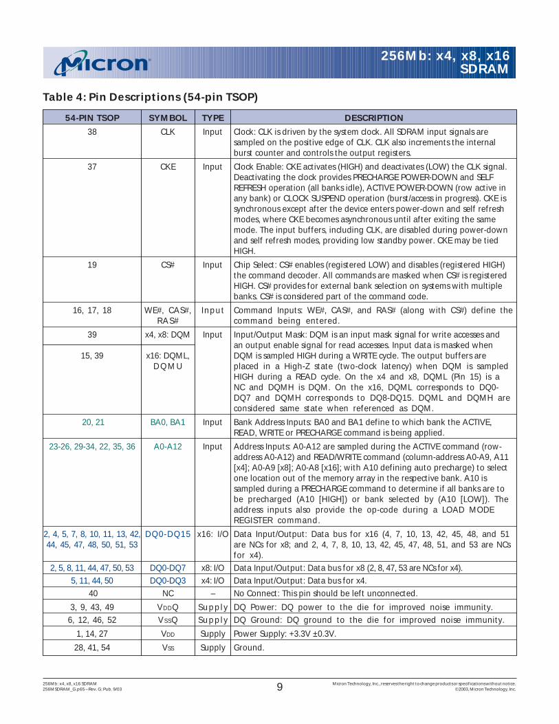
Table 4: Pin Descriptions (54-pin TSOP)
54-PIN TSOP SYMBOL TYPE DESCRIPTION
38 CLK Input Clock: CLK is driven by the system clock. All SDRAM input signals aresampled on the positive edge of CLK. CLK also increments the internalburst counter and controls the output registers.
37 CKE Input Clock Enable: CKE activates (HIGH) and deactivates (LOW) the CLK signal.Deactivating the clock provides PRECHARGE POWER-DOWN and SELFREFRESH operation (all banks idle), ACTIVE POWER-DOWN (row active inany bank) or CLOCK SUSPEND operation (burst/access in progress). CKE issynchronous except after the device enters power-down and self refreshmodes, where CKE becomes asynchronous until after exiting the samemode. The input buffers, including CLK, are disabled during power-downand self refresh modes, providing low standby power. CKE may be tiedHIGH.
19 CS# Input Chip Select: CS# enables (registered LOW) and disables (registered HIGH)the command decoder. All commands are masked when CS# is registeredHIGH. CS# provides for external bank selection on systems with multiplebanks. CS# is considered part of the command code.
16, 17, 18 WE#, CAS#, Input Command Inputs: WE#, CAS#, and RAS# (along with CS#) define theRAS# command being entered.
39 x4, x8: DQM Input Input/Output Mask: DQM is an input mask signal for write accesses andan output enable signal for read accesses. Input data is masked when
15, 39 x16: DQML, DQM is sampled HIGH during a WRITE cycle. The output buffers areDQMU placed in a High-Z state (two-clock latency) when DQM is sampled
HIGH during a READ cycle. On the x4 and x8, DQML (Pin 15) is aNC and DQMH is DQM. On the x16, DQML corresponds to DQ0-DQ7 and DQMH corresponds to DQ8-DQ15. DQML and DQMH areconsidered same state when referenced as DQM.
20, 21 BA0, BA1 Input Bank Address Inputs: BA0 and BA1 define to which bank the ACTIVE,READ, WRITE or PRECHARGE command is being applied.
23-26, 29-34, 22, 35, 36 A0-A12 Input Address Inputs: A0-A12 are sampled during the ACTIVE command (row-address A0-A12) and READ/WRITE command (column-address A0-A9, A11[x4]; A0-A9 [x8]; A0-A8 [x16]; with A10 defining auto precharge) to selectone location out of the memory array in the respective bank. A10 issampled during a PRECHARGE command to determine if all banks are tobe precharged (A10 [HIGH]) or bank selected by (A10 [LOW]). Theaddress inputs also provide the op-code during a LOAD MODEREGISTER command.
2, 4, 5, 7, 8, 10, 11, 13, 42, DQ0-DQ15 x16: I/O Data Input/Output: Data bus for x16 (4, 7, 10, 13, 42, 45, 48, and 5144, 45, 47, 48, 50, 51, 53 are NCs for x8; and 2, 4, 7, 8, 10, 13, 42, 45, 47, 48, 51, and 53 are NCs
for x4).2, 5, 8, 11, 44, 47, 50, 53 DQ0-DQ7 x8: I/O Data Input/Output: Data bus for x8 (2, 8, 47, 53 are NCs for x4).
5, 11, 44, 50 DQ0-DQ3 x4: I/O Data Input/Output: Data bus for x4. 40 NC – No Connect: This pin should be left unconnected.
3, 9, 43, 49 VDDQ Supply DQ Power: DQ power to the die for improved noise immunity.6, 12, 46, 52 VSSQ Supply DQ Ground: DQ ground to the die for improved noise immunity.
1, 14, 27 VDD Supply Power Supply: +3.3V ±0.3V.
28, 41, 54 VSS Supply Ground.
10256Mb: x4, x8, x16 SDRAM Micron Technology, Inc., reserves the right to change products or specifications without notice.256MSDRAM_G.p65 – Rev. G; Pub. 9/03 ©2003, Micron Technology, Inc.
256Mb: x4, x8, x16SDRAM
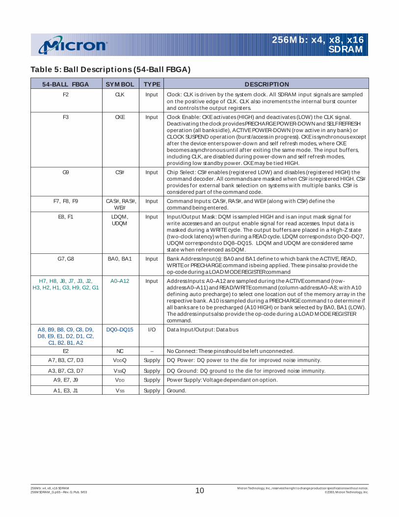
Table 5: Ball Descriptions (54-Ball FBGA)
54-BALL FBGA SYMBOL TYPE DESCRIPTION
F2 CLK Input Clock: CLK is driven by the system clock. All SDRAM input signals are sampledon the positive edge of CLK. CLK also increments the internal burst counterand controls the output registers.
F3 CKE Input Clock Enable: CKE activates (HIGH) and deactivates (LOW) the CLK signal.Deactivating the clock provides PRECHARGE POWER-DOWN and SELF REFRESHoperation (all banks idle), ACTIVE POWER-DOWN (row active in any bank) orCLOCK SUSPEND operation (burst/access in progress). CKE is synchronous exceptafter the device enters power-down and self refresh modes, where CKEbecomes asynchronous until after exiting the same mode. The input buffers,including CLK, are disabled during power-down and self refresh modes,providing low standby power. CKE may be tied HIGH.
G9 CS# Input Chip Select: CS# enables (registered LOW) and disables (registered HIGH) thecommand decoder. All commands are masked when CS# is registered HIGH. CS#provides for external bank selection on systems with multiple banks. CS# isconsidered part of the command code.
F7, F8, F9 CAS#, RAS#, Input Command Inputs: CAS#, RAS#, and WE# (along with CS#) define theWE# command being entered.
E8, F1 LDQM, Input Input/Output Mask: DQM is sampled HIGH and is an input mask signal forUDQM write accesses and an output enable signal for read accesses. Input data is
masked during a WRITE cycle. The output buffers are placed in a High-Z state(two-clock latency) when during a READ cycle. LDQM corresponds to DQ0–DQ7,UDQM corresponds to DQ8–DQ15. LDQM and UDQM are considered samestate when referenced as DQM.
G7, G8 BA0, BA1 Input Bank Address Input(s): BA0 and BA1 define to which bank the ACTIVE, READ,WRITE or PRECHARGE command is being applied. These pins also provide theop-code during a LOAD MODE REGISTER command
H7, H8, J8, J7, J3, J2, A0–A12 Input Address Inputs: A0–A12 are sampled during the ACTIVE command (row-H3, H2, H1, G3, H9, G2, G1 address A0–A11) and READ/WRITE command (column-address A0–A8; with A10
defining auto precharge) to select one location out of the memory array in therespective bank. A10 is sampled during a PRECHARGE command to determine ifall banks are to be precharged (A10 HIGH) or bank selected by BA0, BA1 (LOW).The address inputs also provide the op-code during a LOAD MODE REGISTERcommand.
A8, B9, B8, C9, C8, D9, DQ0–DQ15 I/O Data Input/Output: Data busD8, E9, E1, D2, D1, C2,
C1, B2, B1, A2
E2 NC – No Connect: These pins should be left unconnected.
A7, B3, C7, D3 VDDQ Supply DQ Power: DQ power to the die for improved noise immunity.
A3, B7, C3, D7 VSSQ Supply DQ Ground: DQ ground to the die for improved noise immunity.
A9, E7, J9 VDD Supply Power Supply: Voltage dependant on option.
A1, E3, J1 VSS Supply Ground.
11256Mb: x4, x8, x16 SDRAM Micron Technology, Inc., reserves the right to change products or specifications without notice.256MSDRAM_G.p65 – Rev. G; Pub. 9/03 ©2003, Micron Technology, Inc.
256Mb: x4, x8, x16SDRAM
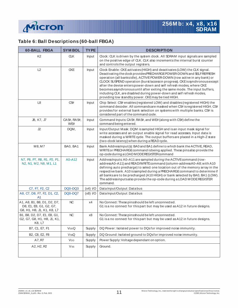
Table 6: Ball Descriptions (60-ball FBGA)
60-BALL FBGA SYMBOL TYPE DESCRIPTION
K2 CLK Input Clock: CLK is driven by the system clock. All SDRAM input signals are sampledon the positive edge of CLK. CLK also increments the internal burst counterand controls the output registers.
L2 CKE Input Clock Enable: CKE activates (HIGH) and deactivates (LOW) the CLK signal.Deactivating the clock provides PRECHARGE POWER-DOWN and SELF REFRESHoperation (all banks idle), ACTIVE POWER-DOWN (row active in any bank) orCLOCK SUSPEND operation (burst/access in progress). CKE is synchronous exceptafter the device enters power-down and self refresh modes, where CKEbecomes asynchronous until after exiting the same mode. The input buffers,including CLK, are disabled during power-down and self refresh modes,providing low standby power. CKE may be tied HIGH.
L8 CS# Input Chip Select: CS# enables (registered LOW) and disables (registered HIGH) thecommand decoder. All commands are masked when CS# is registered HIGH. CS#provides for external bank selection on systems with multiple banks. CS# isconsidered part of the command code.
J8, K7, J7 CAS#, RAS#, Input Command Inputs: CAS#, RAS#, and WE# (along with CS#) define theWE# command being entered.
J2 DQM, Input Input/Output Mask: DQM is sampled HIGH and is an input mask signal forwrite accesses and an output enable signal for read accesses. Input data ismasked during a WRITE cycle. The output buffers are placed in a High-Z state(two-clock latency) when during a READ cycle.
M8, M7 BA0, BA1 Input Bank Address Input(s): BA0 and BA1 define to which bank the ACTIVE, READ,WRITE or PRECHARGE command is being applied. These pins also provide theop-code during a LOAD MODE REGISTER command
N7, P8, P7, R8, R1, P2, P1, A0–A12 Input Address Inputs: A0–A11 are sampled during the ACTIVE command (row-N2, N1, M2, N8, M1, L1 address A0–A11) and READ/WRITE command (column-address A0–A8; with A10
defining auto precharge) to select one location out of the memory array in therespective bank. A10 is sampled during a PRECHARGE command to determine ifall banks are to be precharged (A10 HIGH) or bank selected by BA0, BA1 (LOW).The address inputs also provide the op-code during a LOAD MODE REGISTERcommand.
C7, F7, F2, C2 DQ0–DQ3 (x4) I/O Data Input/Output: Data bus
A8, C7, D8, F7, F2, D1, C2, DQ0–DQ7 (x8) I/O Data Input/Output: Data busA1
A1, A8, B1, B8, D1, D2, D7, NC x4 No Connect: These pins should be left unconnected.D8, E1, E8, G1, G2, G7, G1 is a no connect for this part but may be used as A12 in future designs.
G8, H1, H8, J1, K1, K8, L7
B1, B8, D2, D7, E1, E8, G1, NC x8 No Connect: These pins should be left unconnected. G2, G7, G8, H1, H8, J1, K1, G1 is a no connect for this part but may be used as A12 in future designs.
K8, L7
B7, C1, E7, F1 VDDQ Supply DQ Power: Isolated power to DQs for improved noise immunity.
B2, C8, E2, F8 VSSQ Supply DQ Ground: Isolated ground to DQs for improved noise immunity.
A7, R7 VDD Supply Power Supply: Voltage dependant on option.
A2, H2, R2 VSS Supply Ground.
12256Mb: x4, x8, x16 SDRAM Micron Technology, Inc., reserves the right to change products or specifications without notice.256MSDRAM_G.p65 – Rev. G; Pub. 9/03 ©2003, Micron Technology, Inc.
256Mb: x4, x8, x16SDRAM
Functional DescriptionIn general, the 256Mb SDRAMs (16 Meg x 4 x 4 banks,
8 Meg x 8 x 4 banks and 4 Meg x 16 x 4 banks) are quad-bank DRAMs that operate at 3.3V and include a syn-chronous interface (all signals are registered on thepositive edge of the clock signal, CLK). Each of the x4’s67,108,864-bit banks is organized as 8,192 rows by 2,048columns by 4 bits. Each of the x8’s 67,108,864-bit banksis organized as 8,192 rows by 1,024 columns by 8 bits.Each of the x16’s 67,108,864-bit banks is organized as8,192 rows by 512 columns by 16 bits.
Read and write accesses to the SDRAM are burstoriented; accesses start at a selected location and con-tinue for a programmed number of locations in a pro-grammed sequence. Accesses begin with the registra-tion of an ACTIVE command, which is then followed bya READ or WRITE command. The address bits regis-tered coincident with the ACTIVE command are usedto select the bank and row to be accessed (BA0 and BA1select the bank, A0–A12 select the row). The addressbits (x4: A0–A9, A11; x8: A0–A9; x16: A0–A8) registeredcoincident with the READ or WRITE command are usedto select the starting column location for the burst ac-cess.
Prior to normal operation, the SDRAM must be ini-tialized. The following sections provide detailed infor-mation covering device initialization, register defini-tion, command descriptions and device operation.
InitializationSDRAMs must be powered up and initialized in a
predefined manner. Operational procedures otherthan those specified may result in undefined opera-tion. Once power is applied to VDD and VDDQ (simulta-neously) and the clock is stable (stable clock is definedas a signal cycling within timing constraints specifiedfor the clock pin), the SDRAM requires a 100µs delayprior to issuing any command other than aCOMMAND INHIBIT or NOP. Starting at some pointduring this 100µs period and continuing at leastthrough the end of this period, COMMAND INHIBIT orNOP commands should be applied.
Once the 100µs delay has been satisfied with atleast one COMMAND INHIBIT or NOP command hav-ing been applied, a PRECHARGE command should beapplied. All banks must then be precharged, therebyplacing the device in the all banks idle state.
Once in the idle state, two AUTO REFRESH cyclesmust be performed. After the AUTO REFRESH cyclesare complete, the SDRAM is ready for mode registerprogramming. Because the mode register will powerup in an unknown state, it should be loaded prior toapplying any operational command.
Register DefinitionMode Register
The mode register is used to define the specific modeof operation of the SDRAM. This definition includesthe selection of a burst length, a burst type, a CASlatency, an operating mode and a write burst mode, asshown in Figure 1. The mode register is programmedvia the LOAD MODE REGISTER command and will re-tain the stored information until it is programmed againor the device loses power.
Mode register bits M0–M2 specify the burst length,M3 specifies the type of burst (sequential or inter-leaved), M4–M6 specify the CAS latency, M7 and M8specify the operating mode, M9 specifies the write burstmode, and M10 and M11 are reserved for future use.Address A12 (M12) is undefined but should be drivenLOW during loading of the mode register.
The mode register must be loaded when all banksare idle, and the controller must wait the specified timebefore initiating the subsequent operation. Violatingeither of these requirements will result in unspecifiedoperation.
Burst LengthRead and write accesses to the SDRAM are burst
oriented, with the burst length being programmable,as shown in Figure 1. The burst length determines themaximum number of column locations that can be ac-cessed for a given READ or WRITE command. Burstlengths of 1, 2, 4 or 8 locations are available for both thesequential and the interleaved burst types, and a full-page burst is available for the sequential type. Thefull-page burst is used in conjunction with the BURSTTERMINATE command to generate arbitrary burstlengths.
Reserved states should not be used, as unknownoperation or incompatibility with future versions mayresult.
When a READ or WRITE command is issued, a blockof columns equal to the burst length is effectively se-lected. All accesses for that burst take place within thisblock, meaning that the burst will wrap within the blockif a boundary is reached. The block is uniquely se-lected by A1–A9, A11 (x4), A1–A9 (x8) or A1–A8 (x16)when the burst length is set to two; by A2–A9, A11 (x4),A2–A9 (x8) or A2–A8 (x16) when the burst length is setto four; and by A3–A9, A11 (x4), A3–A9 (x8) or A3–A8(x16) when the burst length is set to eight. The remain-ing (least significant) address bit(s) is (are) used toselect the starting location within the block. Full-pagebursts wrap within the page if the boundary is reached.
13256Mb: x4, x8, x16 SDRAM Micron Technology, Inc., reserves the right to change products or specifications without notice.256MSDRAM_G.p65 – Rev. G; Pub. 9/03 ©2003, Micron Technology, Inc.
256Mb: x4, x8, x16SDRAM
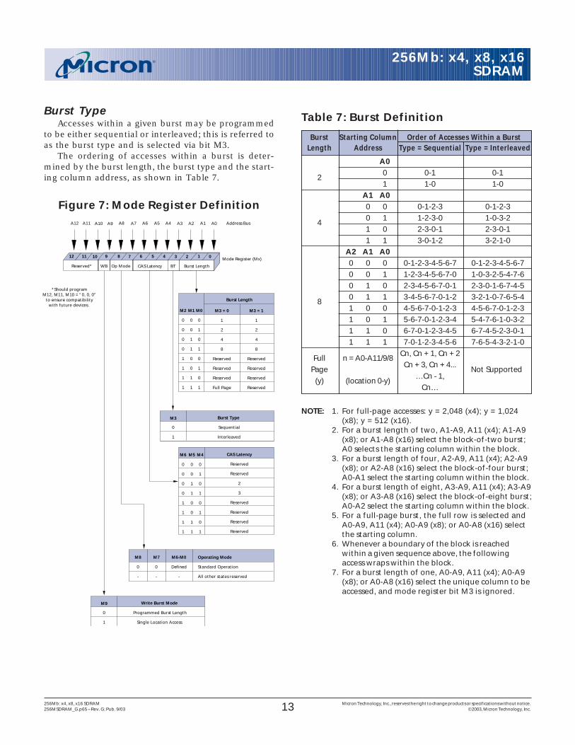
NOTE: 1. For full-page accesses: y = 2,048 (x4); y = 1,024(x8); y = 512 (x16).
2. For a burst length of two, A1-A9, A11 (x4); A1-A9(x8); or A1-A8 (x16) select the block-of-two burst;A0 selects the starting column within the block.
3. For a burst length of four, A2-A9, A11 (x4); A2-A9(x8); or A2-A8 (x16) select the block-of-four burst;A0-A1 select the starting column within the block.
4. For a burst length of eight, A3-A9, A11 (x4); A3-A9(x8); or A3-A8 (x16) select the block-of-eight burst;A0-A2 select the starting column within the block.
5. For a full-page burst, the full row is selected andA0-A9, A11 (x4); A0-A9 (x8); or A0-A8 (x16) selectthe starting column.
6. Whenever a boundary of the block is reachedwithin a given sequence above, the followingaccess wraps within the block.
7. For a burst length of one, A0-A9, A11 (x4); A0-A9(x8); or A0-A8 (x16) select the unique column to beaccessed, and mode register bit M3 is ignored.
Table 7: Burst Definition
Burst Starting Column Order of Accesses Within a BurstLength Address Type = Sequential Type = Interleaved
A0
20 0-1 0-11 1-0 1-0
A1 A00 0 0-1-2-3 0-1-2-3
40 1 1-2-3-0 1-0-3-21 0 2-3-0-1 2-3-0-11 1 3-0-1-2 3-2-1-0
A2 A1 A00 0 0 0-1-2-3-4-5-6-7 0-1-2-3-4-5-6-70 0 1 1-2-3-4-5-6-7-0 1-0-3-2-5-4-7-60 1 0 2-3-4-5-6-7-0-1 2-3-0-1-6-7-4-5
80 1 1 3-4-5-6-7-0-1-2 3-2-1-0-7-6-5-41 0 0 4-5-6-7-0-1-2-3 4-5-6-7-0-1-2-31 0 1 5-6-7-0-1-2-3-4 5-4-7-6-1-0-3-21 1 0 6-7-0-1-2-3-4-5 6-7-4-5-2-3-0-11 1 1 7-0-1-2-3-4-5-6 7-6-5-4-3-2-1-0
Full n = A0-A11/9/8Cn, Cn + 1, Cn + 2
PageCn + 3, Cn + 4...
Not Supported(y) (location 0-y)
…Cn - 1,Cn…
Figure 7: Mode Register Definition
Burst TypeAccesses within a given burst may be programmed
to be either sequential or interleaved; this is referred toas the burst type and is selected via bit M3.
The ordering of accesses within a burst is deter-mined by the burst length, the burst type and the start-ing column address, as shown in Table 7.
M3 = 0
1
2
4
8
Reserved
Reserved
Reserved
Full Page
M3 = 1
1
2
4
8
Reserved
Reserved
Reserved
Reserved
Operating Mode
Standard Operation
All other states reserved
0
-
0
-
Defined
-
0
1
Burst Type
Sequential
Interleaved
CAS Latency
Reserved
Reserved
2
3
Reserved
Reserved
Reserved
Reserved
Burst Length
M0
0
1
0
1
0
1
0
1
Burst LengthCAS Latency BT
A9 A7 A6 A5 A4 A3A8 A2 A1 A0
Mode Register (Mx)
Address Bus
9 7 6 5 4 38 2 1 0
M1
0
0
1
1
0
0
1
1
M2
0
0
0
0
1
1
1
1
M3
M4
0
1
0
1
0
1
0
1
M5
0
0
1
1
0
0
1
1
M6
0
0
0
0
1
1
1
1
M6-M0M8 M7
Op Mode
A10A11
1011
Reserved* WB
0
1
Write Burst Mode
Programmed Burst Length
Single Location Access
M9
*Should programM12, M11, M10 = “0, 0, 0”
to ensure compatibilitywith future devices.
A12
12
14256Mb: x4, x8, x16 SDRAM Micron Technology, Inc., reserves the right to change products or specifications without notice.256MSDRAM_G.p65 – Rev. G; Pub. 9/03 ©2003, Micron Technology, Inc.
256Mb: x4, x8, x16SDRAM
Operating ModeThe normal operating mode is selected by setting
M7 and M8 to zero; the other combinations of values forM7 and M8 are reserved for future use and/or testmodes. The programmed burst length applies to bothREAD and WRITE bursts.
Test modes and reserved states should not be usedbecause unknown operation or incompatibility withfuture versions may result.
Write Burst ModeWhen M9 = 0, the burst length programmed via
M0-M2 applies to both READ and WRITE bursts; whenM9 = 1, the programmed burst length applies to READbursts, but write accesses are single-location (nonburst)accesses.
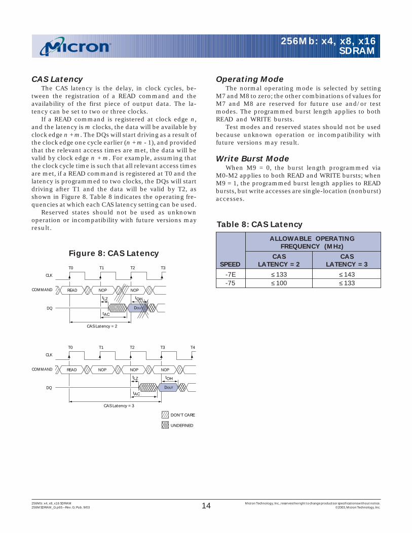
CAS LatencyThe CAS latency is the delay, in clock cycles, be-
tween the registration of a READ command and theavailability of the first piece of output data. The la-tency can be set to two or three clocks.
If a READ command is registered at clock edge n,and the latency is m clocks, the data will be available byclock edge n + m. The DQs will start driving as a result ofthe clock edge one cycle earlier (n + m - 1), and providedthat the relevant access times are met, the data will bevalid by clock edge n + m. For example, assuming thatthe clock cycle time is such that all relevant access timesare met, if a READ command is registered at T0 and thelatency is programmed to two clocks, the DQs will startdriving after T1 and the data will be valid by T2, asshown in Figure 8. Table 8 indicates the operating fre-quencies at which each CAS latency setting can be used.
Reserved states should not be used as unknownoperation or incompatibility with future versions mayresult.
Figure 8: CAS Latency
CLK
DQ
T2T1 T3T0
CAS Latency = 3
LZ
DOUT
tOHt
COMMAND NOPREAD
tAC
NOP
T4
NOP
DON’T CARE
UNDEFINED
CLK
DQ
T2T1 T3T0
CAS Latency = 2
LZ
DOUT
tOHt
COMMAND NOPREAD
tAC
NOP
Table 8: CAS Latency
ALLOWABLE OPERATINGFREQUENCY (MHz)
CAS CASSPEED LATENCY = 2 LATENCY = 3
-7E ≤ 133 ≤ 143-75 ≤ 100 ≤ 133
15256Mb: x4, x8, x16 SDRAM Micron Technology, Inc., reserves the right to change products or specifications without notice.256MSDRAM_G.p65 – Rev. G; Pub. 9/03 ©2003, Micron Technology, Inc.
256Mb: x4, x8, x16SDRAM
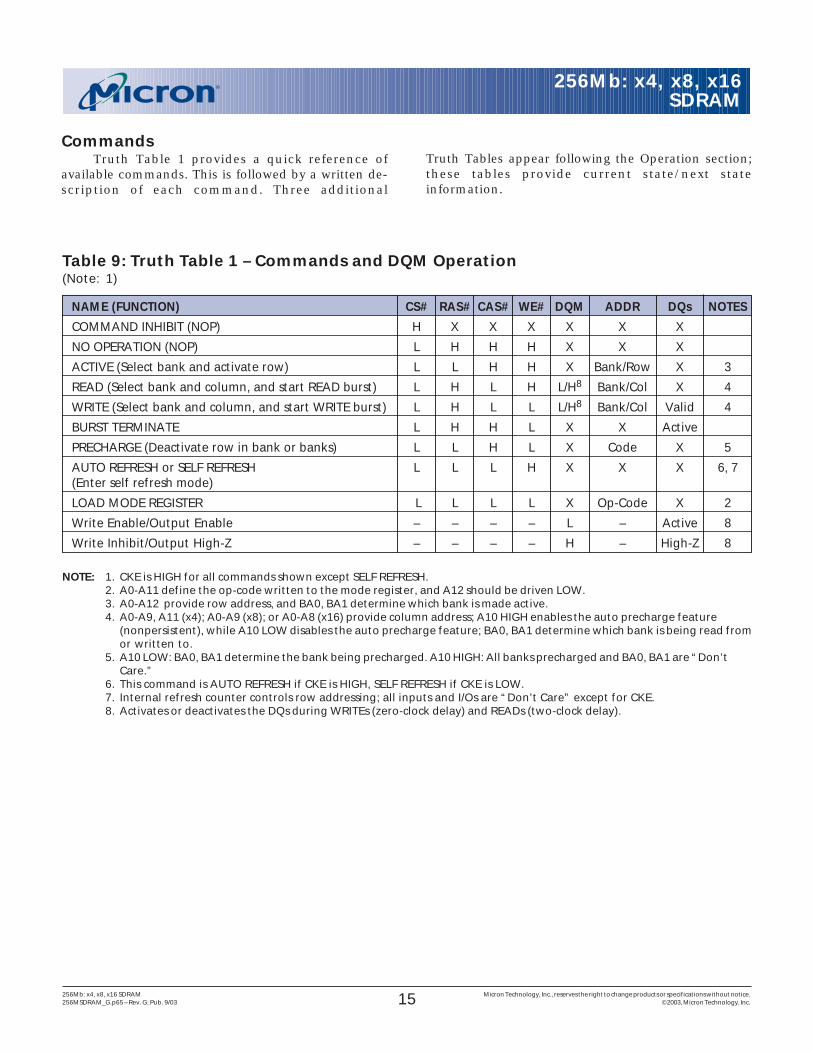
Table 9: Truth Table 1 – Commands and DQM Operation(Note: 1)
NAME (FUNCTION) CS# RAS# CAS# WE# DQM ADDR DQs NOTES
COMMAND INHIBIT (NOP) H X X X X X X
NO OPERATION (NOP) L H H H X X X
ACTIVE (Select bank and activate row) L L H H X Bank/Row X 3
READ (Select bank and column, and start READ burst) L H L H L/H8 Bank/Col X 4
WRITE (Select bank and column, and start WRITE burst) L H L L L/H8 Bank/Col Valid 4
BURST TERMINATE L H H L X X Active
PRECHARGE (Deactivate row in bank or banks) L L H L X Code X 5
AUTO REFRESH or SELF REFRESH L L L H X X X 6, 7(Enter self refresh mode)
LOAD MODE REGISTER L L L L X Op-Code X 2
Write Enable/Output Enable – – – – L – Active 8
Write Inhibit/Output High-Z – – – – H – High-Z 8
Truth Tables appear following the Operation section;these tables provide current state/next stateinformation.
CommandsTruth Table 1 provides a quick reference of
available commands. This is followed by a written de-scription of each command. Three additional
NOTE: 1. CKE is HIGH for all commands shown except SELF REFRESH.2. A0-A11 define the op-code written to the mode register, and A12 should be driven LOW.3. A0-A12 provide row address, and BA0, BA1 determine which bank is made active.4. A0-A9, A11 (x4); A0-A9 (x8); or A0-A8 (x16) provide column address; A10 HIGH enables the auto precharge feature
(nonpersistent), while A10 LOW disables the auto precharge feature; BA0, BA1 determine which bank is being read fromor written to.
5. A10 LOW: BA0, BA1 determine the bank being precharged. A10 HIGH: All banks precharged and BA0, BA1 are “Don’tCare.”
6. This command is AUTO REFRESH if CKE is HIGH, SELF REFRESH if CKE is LOW.7. Internal refresh counter controls row addressing; all inputs and I/Os are “Don’t Care” except for CKE.8. Activates or deactivates the DQs during WRITEs (zero-clock delay) and READs (two-clock delay).
16256Mb: x4, x8, x16 SDRAM Micron Technology, Inc., reserves the right to change products or specifications without notice.256MSDRAM_G.p65 – Rev. G; Pub. 9/03 ©2003, Micron Technology, Inc.
256Mb: x4, x8, x16SDRAM
COMMAND INHIBITThe COMMAND INHIBIT function prevents new
commands from being executed by the SDRAM, re-gardless of whether the CLK signal is enabled. TheSDRAM is effectively deselected. Operations alreadyin progress are not affected.
NO OPERATION (NOP)The NO OPERATION (NOP) command is used to
perform a NOP to an SDRAM which is selected (CS# isLOW). This prevents unwanted commands from beingregistered during idle or wait states. Operations alreadyin progress are not affected.
LOAD MODE REGISTERThe mode register is loaded via inputs A0–A11 (A12
should be driven LOW.) See mode register heading inthe Register Definition section. The LOAD MODE REG-ISTER command can only be issued when all banks areidle, and a subsequent executable command cannotbe issued until tMRD is met.
ACTIVEThe ACTIVE command is used to open (or activate)
a row in a particular bank for a subsequent access. Thevalue on the BA0, BA1 inputs selects the bank, and theaddress provided on inputs A0-A12 selects the row.This row remains active (or open) for accesses until aPRECHARGE command is issued to that bank. APRECHARGE command must be issued before open-ing a different row in the same bank.
READThe READ command is used to initiate a burst read
access to an active row. The value on the BA0, BA1inputs selects the bank, and the address provided oninputs A0-A9, A11 (x4), A0-A9 (x8), or A0-A8 (x16) se-lects the starting column location. The value on inputA10 determines whether or not auto precharge is used.If auto precharge is selected, the row being accessedwill be precharged at the end of the READ burst; if autoprecharge is not selected, the row will remain open forsubsequent accesses. Read data appears on the DQssubject to the logic level on the DQM inputs two clocksearlier. If a given DQM signal was registered HIGH, thecorresponding DQs will be High-Z two clocks later; ifthe DQM signal was registered LOW, the DQs will pro-vide valid data.
WRITEThe WRITE command is used to initiate a burst write
access to an active row. The value on the BA0, BA1inputs selects the bank, and the address provided on
inputs A0-A9; A11 (x4); A0-A9 (x8); or A0-A8 (x16) se-lects the starting column location. The value on inputA10 determines whether or not auto precharge is used.If auto precharge is selected, the row being accessedwill be precharged at the end of the WRITE burst; ifauto precharge is not selected, the row will remain openfor subsequent accesses. Input data appearing on theDQs is written to the memory array subject to the DQMinput logic level appearing coincident with the data. Ifa given DQM signal is registered LOW, the correspond-ing data will be written to memory; if the DQM signal isregistered HIGH, the corresponding data inputs willbe ignored, and a WRITE will not be executed to thatbyte/column location.
PRECHARGEThe PRECHARGE command is used to deactivate
the open row in a particular bank or the open row in allbanks. The bank(s) will be available for a subsequentrow access a specified time (tRP) after the PRECHARGEcommand is issued. Input A10 determines whetherone or all banks are to be precharged, and in the casewhere only one bank is to be precharged, inputs BA0,BA1 select the bank. Otherwise BA0, BA1 are treated as“Don’t Care.” Once a bank has been precharged, it is inthe idle state and must be activated prior to any READor WRITE commands being issued to that bank.
AUTO PRECHARGEAuto precharge is a feature which performs the
same individual-bank PRECHARGE function de-scribed above, without requiring an explicit command.This is accomplished by using A10 to enable autoprecharge in conjunction with a specific READ or WRITEcommand. A PRECHARGE of the bank/row that is ad-dressed with the READ or WRITE command is auto-matically performed upon completion of the READ orWRITE burst, except in the full-page burst mode, whereAUTO PRECHARGE does not apply. Auto precharge isnonpersistent in that it is either enabled or disabled foreach individual READ or WRITE command.
Auto precharge ensures that the precharge is initi-ated at the earliest valid stage within a burst. The usermust not issue another command to the same bankuntil the precharge time (tRP) is completed. This isdetermined as if an explicit PRECHARGE commandwas issued at the earliest possible time, as describedfor each burst type in the Operation section of this datasheet.
BURST TERMINATEThe BURST TERMINATE command is used to trun-
cate either fixed-length or full-page bursts. The most
17256Mb: x4, x8, x16 SDRAM Micron Technology, Inc., reserves the right to change products or specifications without notice.256MSDRAM_G.p65 – Rev. G; Pub. 9/03 ©2003, Micron Technology, Inc.
256Mb: x4, x8, x16SDRAM
recently registered READ or WRITE command prior tothe BURST TERMINATE command will be truncated,as shown in the Operation section of this data sheet.
AUTO REFRESHAUTO REFRESH is used during normal operation of
the SDRAM and is analogous to CAS#-BEFORE-RAS#(CBR) REFRESH in conventional DRAMs. Thiscommand is nonpersistent, so it must be issued eachtime a refresh is required. All active banks must beprecharged prior to issuing an AUTO REFRESH com-mand. The AUTO REFRESH command should not beissued until the minimum tRP has been met after thePRECHARGE command as shown in the operations sec-tion.
The addressing is generated by the internal refreshcontroller. This makes the address bits “Don’t Care”during an AUTO REFRESH command. The 256MbSDRAM requires 8,192 AUTO REFRESH cycles every64ms (tREF), regardless of width option. Providing adistributed AUTO REFRESH command every 7.81µswill meet the refresh requirement and ensure that eachrow is refreshed. Alternatively, 8,192 AUTO REFRESHcommands can be issued in a burst at the minimumcycle rate (tRFC), once every 64ms.
SELF REFRESHThe SELF REFRESH command can be used to retain
data in the SDRAM, even if the rest of the system ispowered down. When in the self refresh mode, theSDRAM retains data without external clocking.The SELF REFRESH command is initiated like an AUTOREFRESH command except CKE is disabled (LOW).Once the SELF REFRESH command is registered, allthe inputs to the SDRAM become “Don’t Care” withthe exception of CKE, which must remain LOW.
Once self refresh mode is engaged, the SDRAM pro-vides its own internal clocking, causing it to perform itsown AUTO REFRESH cycles. The SDRAM must remainin self refresh mode for a minimum period equal totRAS and may remain in self refresh mode for an indefi-nite period beyond that.
The procedure for exiting self refresh requires a se-quence of commands. First, CLK must be stable (stableclock is defined as a signal cycling within timing con-straints specified for the clock pin) prior to CKE goingback HIGH. Once CKE is HIGH, the SDRAM must haveNOP commands issued (a minimum of two clocks) fortXSR because time is required for the completion of anyinternal refresh in progress.
Upon exiting the self refresh mode, AUTO REFRESHcommands must be issued every 7.81µs or less as bothSELF REFRESH and AUTO REFRESH utilize the rowrefresh counter.
18256Mb: x4, x8, x16 SDRAM Micron Technology, Inc., reserves the right to change products or specifications without notice.256MSDRAM_G.p65 – Rev. G; Pub. 9/03 ©2003, Micron Technology, Inc.
256Mb: x4, x8, x16SDRAM
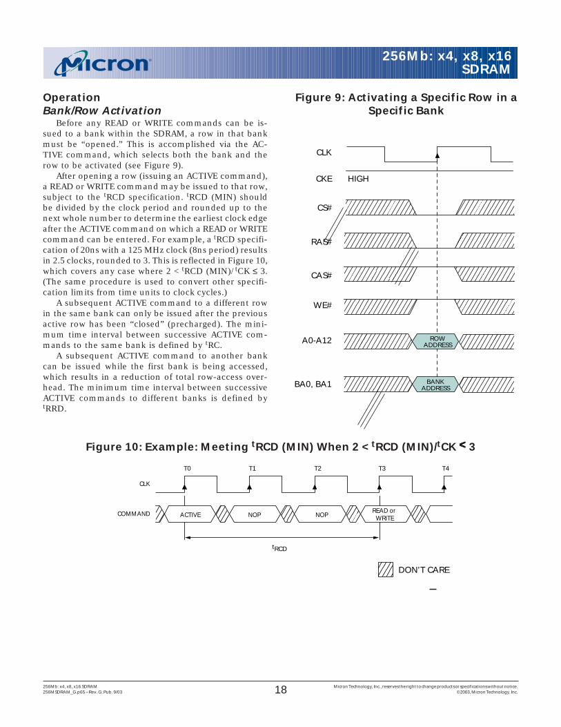
OperationBank/Row Activation
Before any READ or WRITE commands can be is-sued to a bank within the SDRAM, a row in that bankmust be “opened.” This is accomplished via the AC-TIVE command, which selects both the bank and therow to be activated (see Figure 9).
After opening a row (issuing an ACTIVE command),a READ or WRITE command may be issued to that row,subject to the tRCD specification. tRCD (MIN) shouldbe divided by the clock period and rounded up to thenext whole number to determine the earliest clock edgeafter the ACTIVE command on which a READ or WRITEcommand can be entered. For example, a tRCD specifi-cation of 20ns with a 125 MHz clock (8ns period) resultsin 2.5 clocks, rounded to 3. This is reflected in Figure 10,which covers any case where 2 < tRCD (MIN)/tCK ≤ 3.(The same procedure is used to convert other specifi-cation limits from time units to clock cycles.)
A subsequent ACTIVE command to a different rowin the same bank can only be issued after the previousactive row has been “closed” (precharged). The mini-mum time interval between successive ACTIVE com-mands to the same bank is defined by tRC.
A subsequent ACTIVE command to another bankcan be issued while the first bank is being accessed,which results in a reduction of total row-access over-head. The minimum time interval between successiveACTIVE commands to different banks is defined bytRRD.
Figure 10: Example: Meeting tRCD (MIN) When 2 < tRCD (MIN)/tCK <<<<< 3
CLK
T2T1 T3T0
t
COMMAND NOPACTIVEREAD or
WRITE
T4
NOP
RCD
DON’T CARE
Figure 9: Activating a Specific Row in aSpecific Bank
CS#
WE#
CAS#
RAS#
CKE
CLK
A0-A12 ROWADDRESS
HIGH
BA0, BA1 BANKADDRESS
19256Mb: x4, x8, x16 SDRAM Micron Technology, Inc., reserves the right to change products or specifications without notice.256MSDRAM_G.p65 – Rev. G; Pub. 9/03 ©2003, Micron Technology, Inc.
256Mb: x4, x8, x16SDRAM
each possible CAS latency setting.Upon completion of a burst, assuming no other com-
mands have been initiated, the DQs will go High-Z. Afull-page burst will continue until terminated. (At theend of the page, it will wrap to the start address andcontinue.)
Data from any READ burst may be truncated with asubsequent READ command, and data from a fixed-length READ burst may be immediately followed bydata from a READ command. In either case, a continu-ous flow of data can be maintained. The first data ele-ment from the new burst follows either the last ele-ment of a completed burst or the last desired data ele-ment of a longer burst that is being truncated. The newREAD command should be issued x cycles before theclock edge at which the last desired data element is
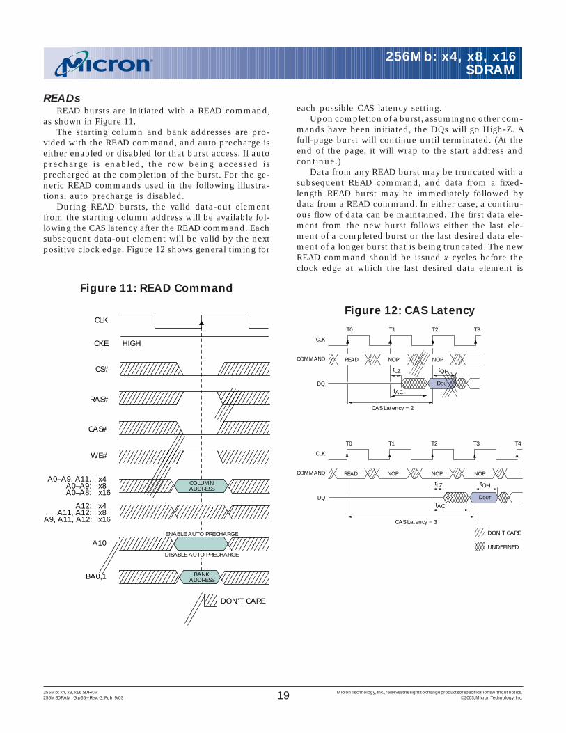
READsREAD bursts are initiated with a READ command,
as shown in Figure 11.The starting column and bank addresses are pro-
vided with the READ command, and auto precharge iseither enabled or disabled for that burst access. If autoprecharge is enabled, the row being accessed isprecharged at the completion of the burst. For the ge-neric READ commands used in the following illustra-tions, auto precharge is disabled.
During READ bursts, the valid data-out elementfrom the starting column address will be available fol-lowing the CAS latency after the READ command. Eachsubsequent data-out element will be valid by the nextpositive clock edge. Figure 12 shows general timing for
Figure 11: READ Command
Figure 12: CAS Latency
CLK
DQ
T2T1 T3T0
CAS Latency = 3
LZ
DOUT
tOHt
COMMAND NOPREAD
tAC
NOP
T4
NOP
DON’T CARE
UNDEFINED
CLK
DQ
T2T1 T3T0
CAS Latency = 2
LZ
DOUT
tOHt
COMMAND NOPREAD
tAC
NOP
CS#
WE#
CAS#
RAS#
CKE
CLK
COLUMNADDRESS
x4 A0–A9: x8 A0–A8: x16
A0–A9, A11:
A10
BA0,1
DON’T CARE
HIGH
ENABLE AUTO PRECHARGE
DISABLE AUTO PRECHARGE
BANKADDRESS
A12: x4 A11, A12: x8A9, A11, A12: x16
20256Mb: x4, x8, x16 SDRAM Micron Technology, Inc., reserves the right to change products or specifications without notice.256MSDRAM_G.p65 – Rev. G; Pub. 9/03 ©2003, Micron Technology, Inc.
256Mb: x4, x8, x16SDRAM
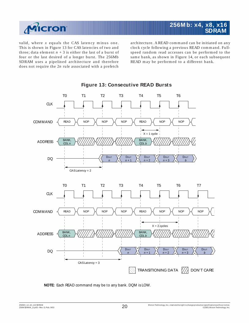
valid, where x equals the CAS latency minus one.This is shown in Figure 13 for CAS latencies of two andthree; data element n + 3 is either the last of a burst offour or the last desired of a longer burst. The 256MbSDRAM uses a pipelined architecture and thereforedoes not require the 2n rule associated with a prefetch
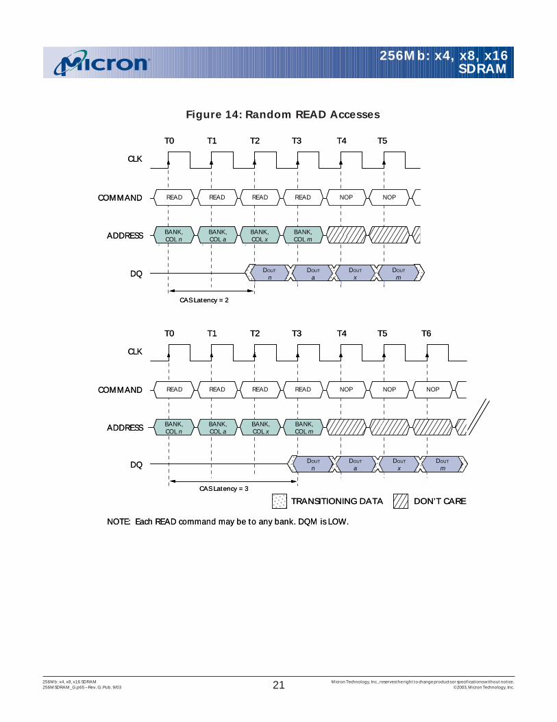
architecture. A READ command can be initiated on anyclock cycle following a previous READ command. Full-speed random read accesses can be performed to thesame bank, as shown in Figure 14, or each subsequentREAD may be performed to a different bank.
Figure 13: Consecutive READ Bursts
DON’T CARE
NOTE: Each READ command may be to any bank. DQM is LOW.
CLK
DQ DOUT
n
T2T1 T4T3 T6T5T0
COMMAND
ADDRESS
READ NOP NOP NOP NOP
BANK,COL n
NOP
BANK,COL b
DOUT
n + 1DOUT
n + 2DOUT
n + 3DOUT
b
READ
X = 1 cycle
CAS Latency = 2
CLK
DQ DOUT
n
T2T1 T4T3 T6T5T0
COMMAND
ADDRESS
READ NOP NOP NOP NOP
BANK,COL n
NOP
BANK,COL b
DOUT
n + 1DOUT
n + 2DOUT
n + 3DOUT
b
READ NOP
T7
X = 2 cycles
CAS Latency = 3
TRANSITIONING DATA
21256Mb: x4, x8, x16 SDRAM Micron Technology, Inc., reserves the right to change products or specifications without notice.256MSDRAM_G.p65 – Rev. G; Pub. 9/03 ©2003, Micron Technology, Inc.
256Mb: x4, x8, x16SDRAM
CLK
DQ
T2T1 T4T3 T6T5T0
COMMAND
ADDRESS
READ NOP NOP
BANK,COL n
DON’T CARE
DOUT
nDOUT
aDOUT
xDOUT
m
READ
NOTE: Each READ command may be to any bank. DQM is LOW.
READ READ NOP
BANK,COL a
BANK,COL x
BANK,COL m
CLK
DQ DOUT
n
T2T1 T4T3 T5T0
COMMAND
ADDRESS
READ NOP
BANK,COL n
DOUT
aDOUT
xDOUT
m
READ READ READ NOP
BANK,COL a
BANK,COL x
BANK,COL m
CAS Latency = 2
CAS Latency = 3
TRANSITIONING DATA
Figure 14: Random READ Accesses
CLK
DQ
T2T1 T4T3 T6T5T0
COMMAND
ADDRESS
READ NOP NOP
BANK,COL n
DON’T CARE
DOUT
nDOUT
aDOUT
xDOUT
m
READ
NOTE: Each READ command may be to any bank. DQM is LOW.
READ READ NOP
BANK,COL a
BANK,COL x
BANK,COL m
CLK
DQ DOUT
n
T2T1 T4T3 T5T0
COMMAND
ADDRESS
READ NOP
BANK,COL n
DOUT
aDOUT
xDOUT
m
READ READ READ NOP
BANK,COL a
BANK,COL x
BANK,COL m
CAS Latency = 2
CAS Latency = 3
TRANSITIONING DATA
22256Mb: x4, x8, x16 SDRAM Micron Technology, Inc., reserves the right to change products or specifications without notice.256MSDRAM_G.p65 – Rev. G; Pub. 9/03 ©2003, Micron Technology, Inc.
256Mb: x4, x8, x16SDRAM
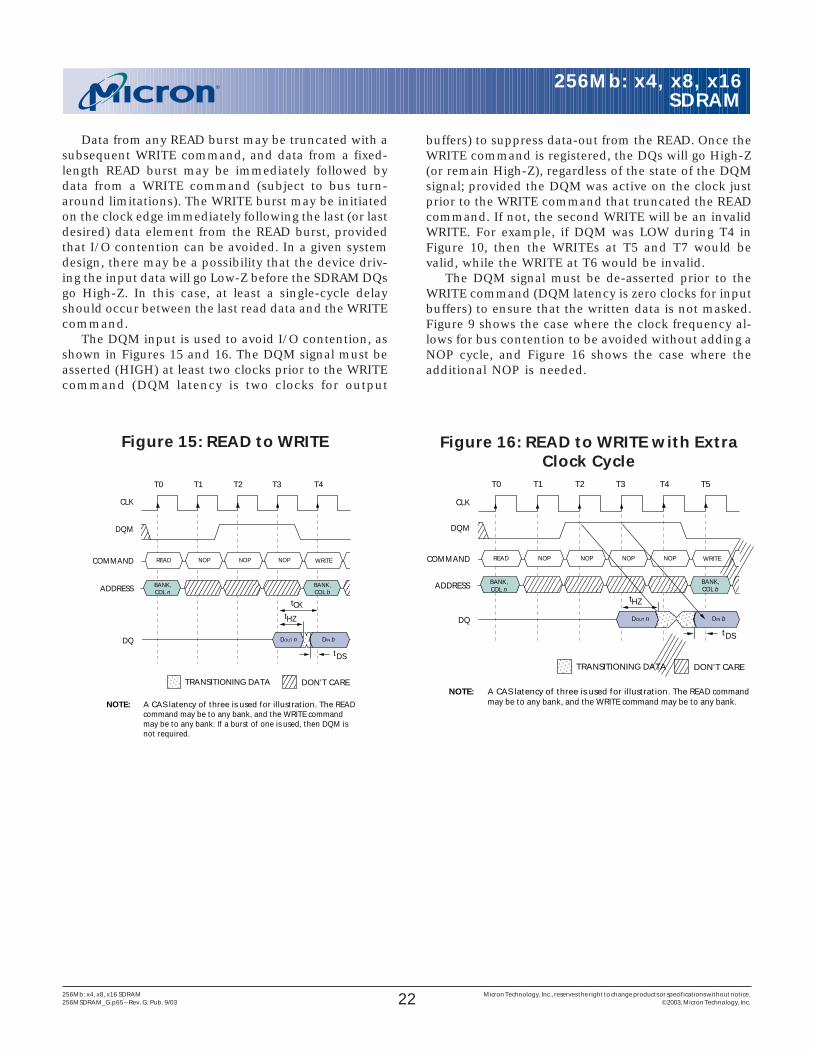
Data from any READ burst may be truncated with asubsequent WRITE command, and data from a fixed-length READ burst may be immediately followed bydata from a WRITE command (subject to bus turn-around limitations). The WRITE burst may be initiatedon the clock edge immediately following the last (or lastdesired) data element from the READ burst, providedthat I/O contention can be avoided. In a given systemdesign, there may be a possibility that the device driv-ing the input data will go Low-Z before the SDRAM DQsgo High-Z. In this case, at least a single-cycle delayshould occur between the last read data and the WRITEcommand.
The DQM input is used to avoid I/O contention, asshown in Figures 15 and 16. The DQM signal must beasserted (HIGH) at least two clocks prior to the WRITEcommand (DQM latency is two clocks for output
buffers) to suppress data-out from the READ. Once theWRITE command is registered, the DQs will go High-Z(or remain High-Z), regardless of the state of the DQMsignal; provided the DQM was active on the clock justprior to the WRITE command that truncated the READcommand. If not, the second WRITE will be an invalidWRITE. For example, if DQM was LOW during T4 inFigure 10, then the WRITEs at T5 and T7 would bevalid, while the WRITE at T6 would be invalid.
The DQM signal must be de-asserted prior to theWRITE command (DQM latency is zero clocks for inputbuffers) to ensure that the written data is not masked.Figure 9 shows the case where the clock frequency al-lows for bus contention to be avoided without adding aNOP cycle, and Figure 16 shows the case where theadditional NOP is needed.
DON’T CARE
READ NOP NOPNOP NOP
DQM
CLK
DQ DOUT n
T2T1 T4T3T0
COMMAND
ADDRESS BANK,COL n
WRITE
DIN b
BANK,COL b
T5
DS
tHZ
t
NOTE: A CAS latency of three is used for illustration. The READ command may be to any bank, and the WRITE command may be to any bank.
TRANSITIONING DATA
Figure 16: READ to WRITE with ExtraClock Cycle
Figure 15: READ to WRITE
DON’T CARE
READ NOP NOP WRITENOP
CLK
T2T1 T4T3T0
DQM
DQ DOUT n
COMMAND
DIN b
ADDRESS BANK,COL n
BANK,COL b
DS
tHZ
t
tCK
NOTE: A CAS latency of three is used for illustration. The READ command may be to any bank, and the WRITE command may be to any bank. If a burst of one is used, then DQM is not required.
TRANSITIONING DATA
23256Mb: x4, x8, x16 SDRAM Micron Technology, Inc., reserves the right to change products or specifications without notice.256MSDRAM_G.p65 – Rev. G; Pub. 9/03 ©2003, Micron Technology, Inc.
256Mb: x4, x8, x16SDRAM
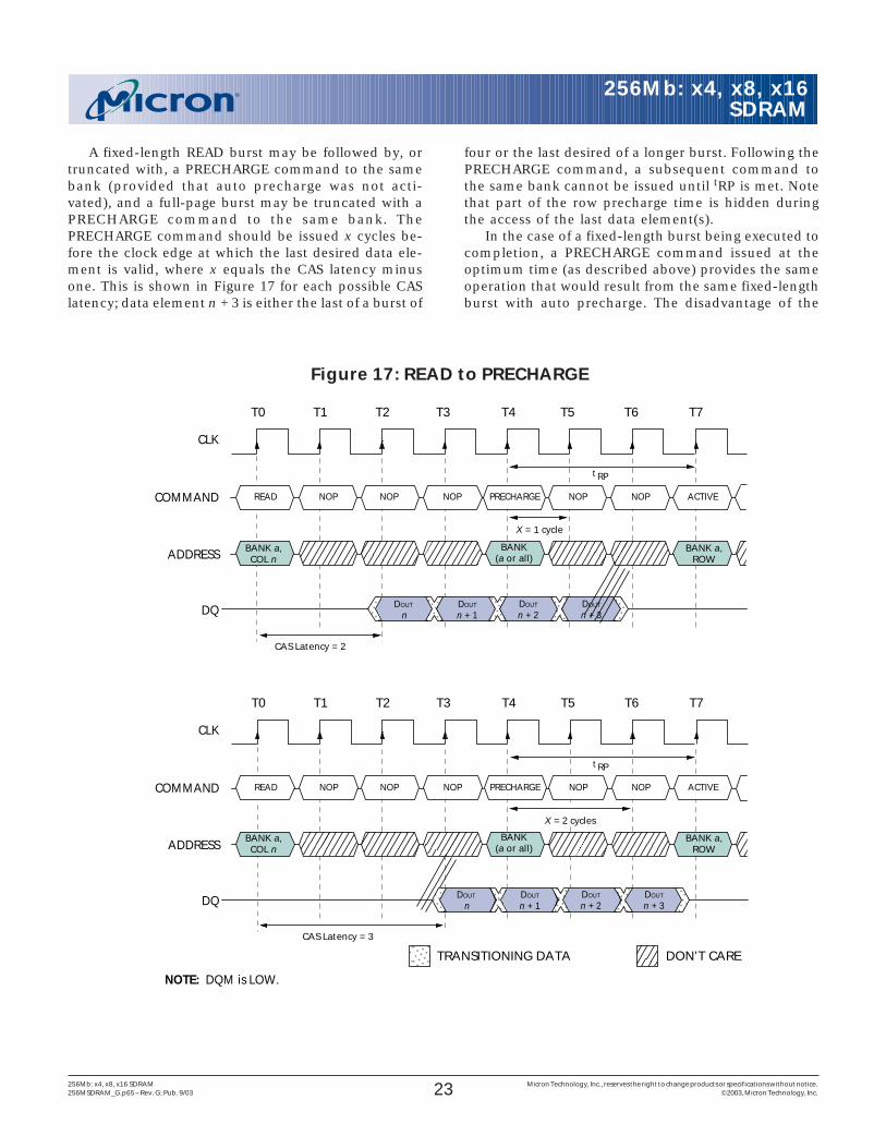
A fixed-length READ burst may be followed by, ortruncated with, a PRECHARGE command to the samebank (provided that auto precharge was not acti-vated), and a full-page burst may be truncated with aPRECHARGE command to the same bank. ThePRECHARGE command should be issued x cycles be-fore the clock edge at which the last desired data ele-ment is valid, where x equals the CAS latency minusone. This is shown in Figure 17 for each possible CASlatency; data element n + 3 is either the last of a burst of
four or the last desired of a longer burst. Following thePRECHARGE command, a subsequent command tothe same bank cannot be issued until tRP is met. Notethat part of the row precharge time is hidden duringthe access of the last data element(s).
In the case of a fixed-length burst being executed tocompletion, a PRECHARGE command issued at theoptimum time (as described above) provides the sameoperation that would result from the same fixed-lengthburst with auto precharge. The disadvantage of the
Figure 17: READ to PRECHARGE
DON’T CARE
CLK
DQ DOUT
n
T2T1 T4T3 T6T5T0
COMMAND
ADDRESS
READ NOP NOP NOP NOPNOP
DOUT
n + 1DOUT
n + 2DOUT
n + 3
PRECHARGE ACTIVE
t RP
T7
NOTE: DQM is LOW.
CLK
DQ DOUT
n
T2T1 T4T3 T6T5T0
COMMAND
ADDRESS
READ NOP NOP NOP NOPNOP
DOUT
n + 1DOUT
n + 2DOUT
n + 3
PRECHARGE ACTIVE
t RP
T7
X = 1 cycle
CAS Latency = 2
CAS Latency = 3
X = 2 cycles
BANK a,COL n
BANK a,ROW
BANK(a or all)
BANK a,COL n
BANK a,ROW
BANK(a or all)
TRANSITIONING DATA
24256Mb: x4, x8, x16 SDRAM Micron Technology, Inc., reserves the right to change products or specifications without notice.256MSDRAM_G.p65 – Rev. G; Pub. 9/03 ©2003, Micron Technology, Inc.
256Mb: x4, x8, x16SDRAM
PRECHARGE command is that it requires that the com-mand and address buses be available at the appropri-ate time to issue the command; the advantage of thePRECHARGE command is that it can be used to trun-cate fixed-length or full-page bursts.
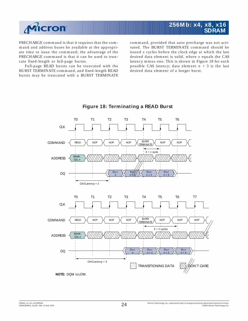
Full-page READ bursts can be truncated with theBURST TERMINATE command, and fixed-length READbursts may be truncated with a BURST TERMINATE
command, provided that auto precharge was not acti-vated. The BURST TERMINATE command should beissued x cycles before the clock edge at which the lastdesired data element is valid, where x equals the CASlatency minus one. This is shown in Figure 18 for eachpossible CAS latency; data element n + 3 is the lastdesired data element of a longer burst.
Figure 18: Terminating a READ Burst
CLK
DQ DOUT
n
T2T1 T4T3 T6T5T0
COMMAND
ADDRESS
READ NOP NOP NOP NOP
BANK,COL n
NOP
DOUT
n + 1DOUT
n + 2DOUT
n + 3
BURSTTERMINATE
NOP
T7
DON’T CARE
NOTE: DQM is LOW.
CLK
DQ DOUT
n
T2T1 T4T3 T6T5T0
COMMAND
ADDRESS
READ NOP NOP NOP
BANK,COL n
NOP
DOUT
n + 1DOUT
n + 2DOUT
n + 3
BURSTTERMINATE
NOP
X = 1 cycle
CAS Latency = 2
CAS Latency = 3
X = 2 cycles
TRANSITIONING DATA
25256Mb: x4, x8, x16 SDRAM Micron Technology, Inc., reserves the right to change products or specifications without notice.256MSDRAM_G.p65 – Rev. G; Pub. 9/03 ©2003, Micron Technology, Inc.
256Mb: x4, x8, x16SDRAM
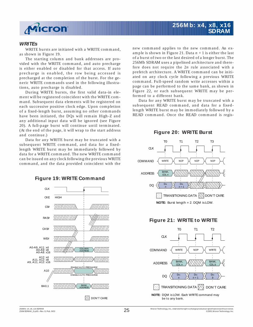
WRITEsWRITE bursts are initiated with a WRITE command,
as shown in Figure 19.The starting column and bank addresses are pro-
vided with the WRITE command, and auto prechargeis either enabled or disabled for that access. If autoprecharge is enabled, the row being accessed isprecharged at the completion of the burst. For the ge-neric WRITE commands used in the following illustra-tions, auto precharge is disabled.
During WRITE bursts, the first valid data-in ele-ment will be registered coincident with the WRITE com-mand. Subsequent data elements will be registered oneach successive positive clock edge. Upon completionof a fixed-length burst, assuming no other commandshave been initiated, the DQs will remain High-Z andany additional input data will be ignored (see Figure20). A full-page burst will continue until terminated.(At the end of the page, it will wrap to the start addressand continue.)
Data for any WRITE burst may be truncated with asubsequent WRITE command, and data for a fixed-length WRITE burst may be immediately followed bydata for a WRITE command. The new WRITE commandcan be issued on any clock following the previous WRITEcommand, and the data provided coincident with the
new command applies to the new command. An ex-ample is shown in Figure 21. Data n + 1 is either the lastof a burst of two or the last desired of a longer burst. The256Mb SDRAM uses a pipelined architecture and there-fore does not require the 2n rule associated with aprefetch architecture. A WRITE command can be initi-ated on any clock cycle following a previous WRITEcommand. Full-speed random write accesses within apage can be performed to the same bank, as shown inFigure 22, or each subsequent WRITE may be per-formed to a different bank.
Data for any WRITE burst may be truncated with asubsequent READ command, and data for a fixed-length WRITE burst may be immediately followed by aREAD command. Once the READ command is regis-
Figure 19: WRITE Command
Figure 21: WRITE to WRITE
Figure 20: WRITE Burst
CLK
DQ
T2T1T0
COMMAND
ADDRESS
NOPWRITE WRITE
BANK,COL n
BANK,COL b
DIN
nDIN
n + 1DIN
b
NOTE: DQM is LOW. Each WRITE command maybe to any bank.
DON’T CARETRANSITIONING DATA
CLK
DQ DIN
n
T2T1 T3T0
COMMAND
ADDRESS
NOP NOP
DON’T CARE
WRITE
DIN
n + 1
NOP
BANK,COL n
NOTE: Burst length = 2. DQM is LOW.
TRANSITIONING DATA
CS#
WE#
CAS#
RAS#
CKE
CLK
COLUMNADDRESS
A10
DON’T CARE
HIGH
ENABLE AUTO PRECHARGE
DISABLE AUTO PRECHARGE
A0-A9, A11: x4 A0-A9: x8 A0-A8: x16
A12: x4 A11, A12: x8
A9, A11, A12: x16
BA0,1 BANKADDRESS
26256Mb: x4, x8, x16 SDRAM Micron Technology, Inc., reserves the right to change products or specifications without notice.256MSDRAM_G.p65 – Rev. G; Pub. 9/03 ©2003, Micron Technology, Inc.
256Mb: x4, x8, x16SDRAM
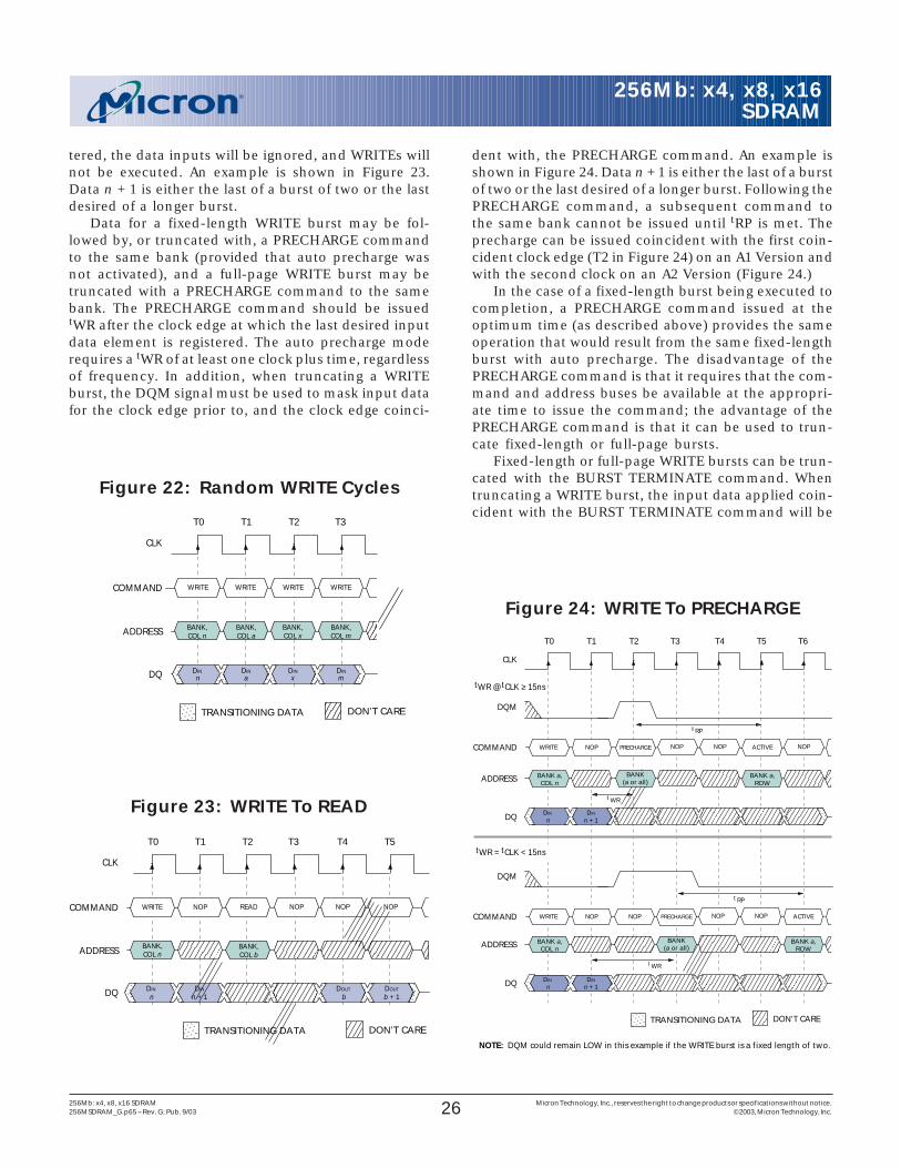
dent with, the PRECHARGE command. An example isshown in Figure 24. Data n + 1 is either the last of a burstof two or the last desired of a longer burst. Following thePRECHARGE command, a subsequent command tothe same bank cannot be issued until tRP is met. Theprecharge can be issued coincident with the first coin-cident clock edge (T2 in Figure 24) on an A1 Version andwith the second clock on an A2 Version (Figure 24.)
In the case of a fixed-length burst being executed tocompletion, a PRECHARGE command issued at theoptimum time (as described above) provides the sameoperation that would result from the same fixed-lengthburst with auto precharge. The disadvantage of thePRECHARGE command is that it requires that the com-mand and address buses be available at the appropri-ate time to issue the command; the advantage of thePRECHARGE command is that it can be used to trun-cate fixed-length or full-page bursts.
Fixed-length or full-page WRITE bursts can be trun-cated with the BURST TERMINATE command. Whentruncating a WRITE burst, the input data applied coin-cident with the BURST TERMINATE command will be
tered, the data inputs will be ignored, and WRITEs willnot be executed. An example is shown in Figure 23.Data n + 1 is either the last of a burst of two or the lastdesired of a longer burst.
Data for a fixed-length WRITE burst may be fol-lowed by, or truncated with, a PRECHARGE commandto the same bank (provided that auto precharge wasnot activated), and a full-page WRITE burst may betruncated with a PRECHARGE command to the samebank. The PRECHARGE command should be issuedtWR after the clock edge at which the last desired inputdata element is registered. The auto precharge moderequires a tWR of at least one clock plus time, regardlessof frequency. In addition, when truncating a WRITEburst, the DQM signal must be used to mask input datafor the clock edge prior to, and the clock edge coinci-
Figure 24: WRITE To PRECHARGE
DON’T CARE
DQM
CLK
DQ
T2T1 T4T3T0
COMMAND
ADDRESS BANK a,COL n
T5
NOPWRITE PRECHARGE NOPNOP
DIN
nDIN
n + 1
ACTIVE
t RP
BANK(a or all)
t WR
BANK a,ROW
DQM
DQ
COMMAND
ADDRESS BANK a,COL n
NOPWRITE PRECHARGE NOPNOP
DIN
nDIN
n + 1
ACTIVE
t RP
BANK(a or all)
t WR
NOTE: DQM could remain LOW in this example if the WRITE burst is a fixed length of two.
BANK a,ROW
T6
NOP
NOP
tWR @ tCLK ≥ 15ns
tWR = tCLK < 15ns
TRANSITIONING DATA
Figure 23: WRITE To READ
DON’T CARE
CLK
DQ
T2T1 T3T0
COMMAND
ADDRESS
NOPWRITE
BANK,COL n
DIN
nDIN
n + 1DOUT
b
READ NOP NOP
BANK,COL b
NOP
DOUT
b + 1
T4 T5
TRANSITIONING DATA
Figure 22: Random WRITE Cycles
DON’T CARE
CLK
DQ DIN
n
T2T1 T3T0
COMMAND
ADDRESS
WRITE
BANK,COL n
DIN
aDIN
xDIN
m
WRITE WRITE WRITE
BANK,COL a
BANK,COL x
BANK,COL m
TRANSITIONING DATA
27256Mb: x4, x8, x16 SDRAM Micron Technology, Inc., reserves the right to change products or specifications without notice.256MSDRAM_G.p65 – Rev. G; Pub. 9/03 ©2003, Micron Technology, Inc.
256Mb: x4, x8, x16SDRAM
ignored. The last data written (provided that DQM isLOW at that time) will be the input data applied oneclock previous to the BURST TERMINATE command.This is shown in Figure 25, where data n is the lastdesired data element of a longer burst.
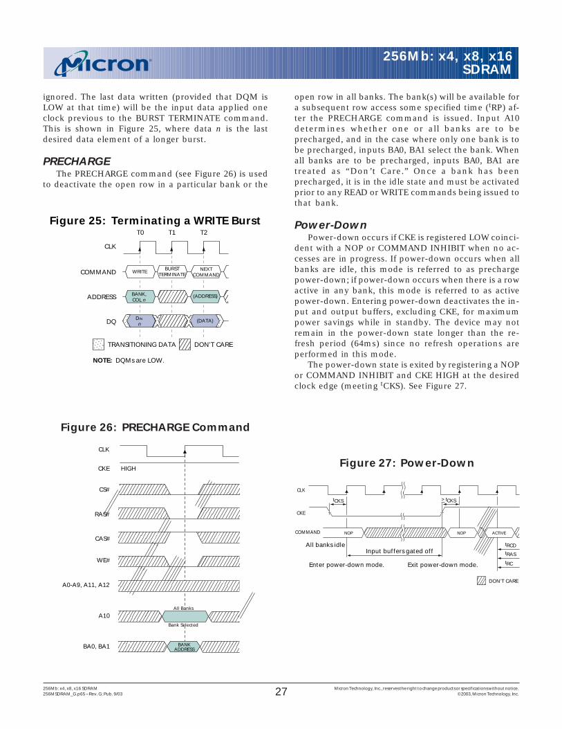
PRECHARGEThe PRECHARGE command (see Figure 26) is used
to deactivate the open row in a particular bank or the
DON’T CARE
tRAS
tRCD
tRC
All banks idleInput buffers gated off
Exit power-down mode.
()()
()()
()()
tCKS > tCKS
COMMAND NOP ACTIVE
Enter power-down mode.
NOP
CLK
CKE
()()
()()
open row in all banks. The bank(s) will be available fora subsequent row access some specified time (tRP) af-ter the PRECHARGE command is issued. Input A10determines whether one or all banks are to beprecharged, and in the case where only one bank is tobe precharged, inputs BA0, BA1 select the bank. Whenall banks are to be precharged, inputs BA0, BA1 aretreated as “Don’t Care.” Once a bank has beenprecharged, it is in the idle state and must be activatedprior to any READ or WRITE commands being issued tothat bank.
Power-DownPower-down occurs if CKE is registered LOW coinci-
dent with a NOP or COMMAND INHIBIT when no ac-cesses are in progress. If power-down occurs when allbanks are idle, this mode is referred to as prechargepower-down; if power-down occurs when there is a rowactive in any bank, this mode is referred to as activepower-down. Entering power-down deactivates the in-put and output buffers, excluding CKE, for maximumpower savings while in standby. The device may notremain in the power-down state longer than the re-fresh period (64ms) since no refresh operations areperformed in this mode.
The power-down state is exited by registering a NOPor COMMAND INHIBIT and CKE HIGH at the desiredclock edge (meeting tCKS). See Figure 27.
CS#
WE#
CAS#
RAS#
CKE
CLK
A10
HIGH
All Banks
Bank Selected
A0-A9, A11, A12
BA0, BA1 BANKADDRESS
Figure 27: Power-Down
Figure 26: PRECHARGE Command
Figure 25: Terminating a WRITE Burst
DON’T CARE
CLK
DQ
T2T1T0
COMMAND
ADDRESS BANK,COL n
WRITE BURSTTERMINATE
NEXTCOMMAND
DIN
n
(ADDRESS)
(DATA)
NOTE: DQMs are LOW.
TRANSITIONING DATA
28256Mb: x4, x8, x16 SDRAM Micron Technology, Inc., reserves the right to change products or specifications without notice.256MSDRAM_G.p65 – Rev. G; Pub. 9/03 ©2003, Micron Technology, Inc.
256Mb: x4, x8, x16SDRAM
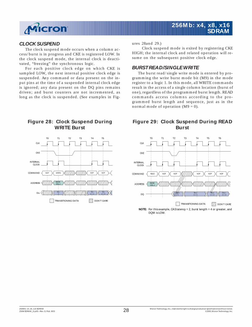
CLOCK SUSPENDThe clock suspend mode occurs when a column ac-
cess/burst is in progress and CKE is registered LOW. Inthe clock suspend mode, the internal clock is deacti-vated, “freezing” the synchronous logic.
For each positive clock edge on which CKE issampled LOW, the next internal positive clock edge issuspended. Any command or data present on the in-put pins at the time of a suspended internal clock edgeis ignored; any data present on the DQ pins remainsdriven; and burst counters are not incremented, aslong as the clock is suspended. (See examples in Fig-
ures 28and 29.)Clock suspend mode is exited by registering CKE
HIGH; the internal clock and related operation will re-sume on the subsequent positive clock edge.
BURST READ/SINGLE WRITEThe burst read/single write mode is entered by pro-
gramming the write burst mode bit (M9) in the moderegister to a logic 1. In this mode, all WRITE commandsresult in the access of a single column location (burst ofone), regardless of the programmed burst length. READcommands access columns according to the pro-grammed burst length and sequence, just as in thenormal mode of operation (M9 = 0).
DON’T CARE
DIN
COMMAND
ADDRESS
WRITE
BANK,COL n
DIN
n
NOPNOP
CLK
T2T1 T4T3 T5T0
CKE
INTERNALCLOCK
NOP
DIN
n + 1DIN
n + 2
TRANSITIONING DATA
Figure 28: Clock Suspend DuringWRITE Burst
DON’T CARE
CLK
DQDOUT
n
T2T1 T4T3 T6T5T0
COMMAND
ADDRESS
READ NOP NOP NOP
BANK,COL n
NOP
DOUT
n + 1DOUT
n + 2DOUT
n + 3
NOTE: For this example, CAS latency = 2, burst length = 4 or greater, and DQM is LOW.
CKE
INTERNALCLOCK
NOP
TRANSITIONING DATA
Figure 29: Clock Suspend During READBurst
29256Mb: x4, x8, x16 SDRAM Micron Technology, Inc., reserves the right to change products or specifications without notice.256MSDRAM_G.p65 – Rev. G; Pub. 9/03 ©2003, Micron Technology, Inc.
256Mb: x4, x8, x16SDRAM
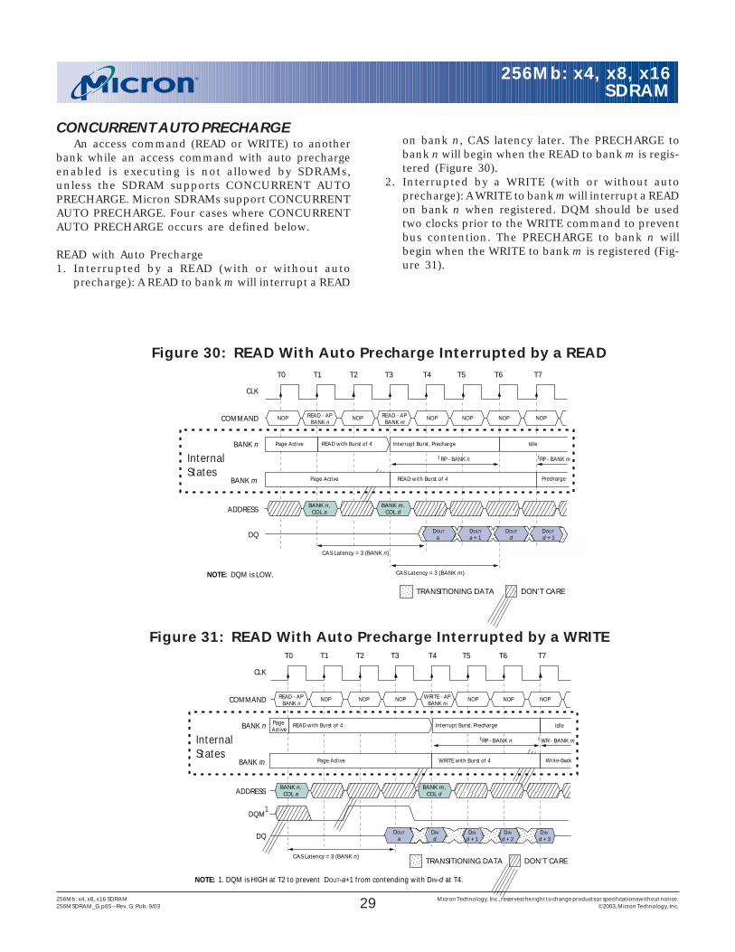
CONCURRENT AUTO PRECHARGEAn access command (READ or WRITE) to another
bank while an access command with auto prechargeenabled is executing is not allowed by SDRAMs,unless the SDRAM supports CONCURRENT AUTOPRECHARGE. Micron SDRAMs support CONCURRENTAUTO PRECHARGE. Four cases where CONCURRENTAUTO PRECHARGE occurs are defined below.
READ with Auto Precharge1. Interrupted by a READ (with or without auto
precharge): A READ to bank m will interrupt a READ
on bank n, CAS latency later. The PRECHARGE tobank n will begin when the READ to bank m is regis-tered (Figure 30).
2. Interrupted by a WRITE (with or without autoprecharge): A WRITE to bank m will interrupt a READon bank n when registered. DQM should be usedtwo clocks prior to the WRITE command to preventbus contention. The PRECHARGE to bank n willbegin when the WRITE to bank m is registered (Fig-ure 31).
Figure 30: READ With Auto Precharge Interrupted by a READ
CLK
DQDOUT
a
T2T1 T4T3 T6T5T0
COMMAND NOPNOPNOPNOP
DIN
d + 1DIN
dDIN
d + 2DIN
d + 3
NOP
T7
BANK n
BANK m
ADDRESS
Idle
NOP
DQM
NOTE: 1. DQM is HIGH at T2 to prevent DOUT-a+1 from contending with DIN-d at T4.
BANK n,COL a
BANK m,COL d
WRITE - AP BANK m
Internal States
t
Page Active
READ with Burst of 4 Interrupt Burst, Precharge
Page Active WRITE with Burst of 4 Write-Back
RP - BANK n t WR - BANK m
CAS Latency = 3 (BANK n)
READ - AP BANK n
1
DON’T CARETRANSITIONING DATA
Figure 31: READ With Auto Precharge Interrupted by a WRITE
DON’T CARE
CLK
DQ DOUT
a
T2T1 T4T3 T6T5T0
COMMAND READ - AP BANK n
NOP NOPNOPNOP
DOUT
a + 1DOUT
dDOUT
d + 1
NOP
T7
BANK n
CAS Latency = 3 (BANK m)
BANK m
ADDRESS
Idle
NOP
NOTE: DQM is LOW.
BANK n,COL a
BANK m,COL d
READ - AP BANK m
Internal States
t
Page Active READ with Burst of 4 Interrupt Burst, Precharge
Page Active READ with Burst of 4 Precharge
RP - BANK n tRP - BANK m
CAS Latency = 3 (BANK n)
TRANSITIONING DATA
30256Mb: x4, x8, x16 SDRAM Micron Technology, Inc., reserves the right to change products or specifications without notice.256MSDRAM_G.p65 – Rev. G; Pub. 9/03 ©2003, Micron Technology, Inc.
256Mb: x4, x8, x16SDRAM
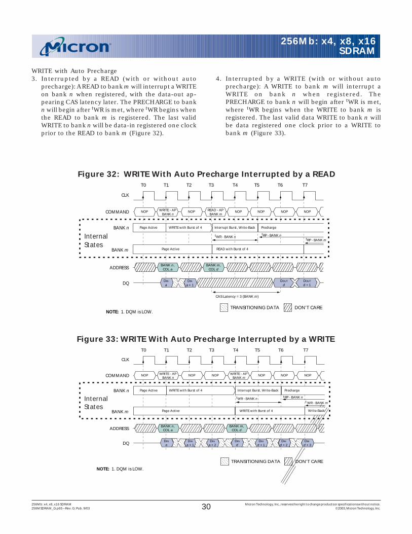
WRITE with Auto Precharge3. Interrupted by a READ (with or without auto
precharge): A READ to bank m will interrupt a WRITEon bank n when registered, with the data-out ap-pearing CAS latency later. The PRECHARGE to bankn will begin after tWR is met, where tWR begins whenthe READ to bank m is registered. The last validWRITE to bank n will be data-in registered one clockprior to the READ to bank m (Figure 32).
4. Interrupted by a WRITE (with or without autoprecharge): A WRITE to bank m will interrupt aWRITE on bank n when registered. ThePRECHARGE to bank n will begin after tWR is met,where tWR begins when the WRITE to bank m isregistered. The last valid data WRITE to bank n willbe data registered one clock prior to a WRITE tobank m (Figure 33).
Figure 32: WRITE With Auto Precharge Interrupted by a READ
DON’T CARE
CLK
DQ
T2T1 T4T3 T6T5T0
COMMAND WRITE - AP BANK n
NOPNOPNOPNOP
DIN
d + 1DIN
dDIN
a + 1DIN
a + 2DIN
aDIN
d + 2DIN
d + 3
NOP
T7
BANK n
BANK m
ADDRESS
NOP
NOTE: 1. DQM is LOW.
BANK n,COL a
BANK m,COL d
WRITE - AP BANK m
Internal States
t
Page Active WRITE with Burst of 4 Interrupt Burst, Write-Back Precharge
Page Active WRITE with Burst of 4 Write-Back
WR - BANK n tRP - BANK nt WR - BANK m
TRANSITIONING DATA
Figure 33: WRITE With Auto Precharge Interrupted by a WRITE
DON’T CARE
CLK
DQ
T2T1 T4T3 T6T5T0
COMMAND WRITE - AP BANK n
NOPNOPNOPNOP
DIN
a + 1DIN
a
NOP NOP
T7
BANK n
BANK m
ADDRESS
NOTE: 1. DQM is LOW.
BANK n,COL a
BANK m,COL d
READ - AP BANK m
Internal States
t
Page Active WRITE with Burst of 4 Interrupt Burst, Write-Back Precharge
Page Active READ with Burst of 4
ttRP - BANK m
DOUT
dDOUT
d + 1
CAS Latency = 3 (BANK m)
RP - BANK nWR - BANK n
TRANSITIONING DATA
31256Mb: x4, x8, x16 SDRAM Micron Technology, Inc., reserves the right to change products or specifications without notice.256MSDRAM_G.p65 – Rev. G; Pub. 9/03 ©2003, Micron Technology, Inc.
256Mb: x4, x8, x16SDRAM
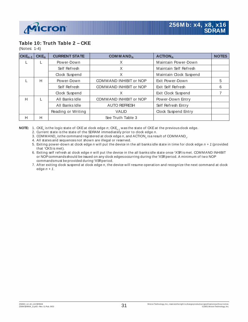
Table 10: Truth Table 2 – CKE(Notes: 1-4)
CKEn-1 CKEn CURRENT STATE COMMANDn ACTIONn NOTES
L L Power-Down X Maintain Power-Down
Self Refresh X Maintain Self Refresh
Clock Suspend X Maintain Clock Suspend
L H Power-Down COMMAND INHIBIT or NOP Exit Power-Down 5
Self Refresh COMMAND INHIBIT or NOP Exit Self Refresh 6
Clock Suspend X Exit Clock Suspend 7
H L All Banks Idle COMMAND INHIBIT or NOP Power-Down Entry
All Banks Idle AUTO REFRESH Self Refresh Entry
Reading or Writing VALID Clock Suspend Entry
H H See Truth Table 3
NOTE: 1. CKEn is the logic state of CKE at clock edge n; CKEn-1 was the state of CKE at the previous clock edge.2. Current state is the state of the SDRAM immediately prior to clock edge n.3. COMMANDn is the command registered at clock edge n, and ACTIONn is a result of COMMANDn.4. All states and sequences not shown are illegal or reserved.5. Exiting power-down at clock edge n will put the device in the all banks idle state in time for clock edge n + 1 (provided
that tCKS is met).6. Exiting self refresh at clock edge n will put the device in the all banks idle state once tXSR is met. COMMAND INHIBIT
or NOP commands should be issued on any clock edges occurring during the tXSR period. A minimum of two NOPcommands must be provided during tXSR period.
7. After exiting clock suspend at clock edge n, the device will resume operation and recognize the next command at clockedge n + 1.
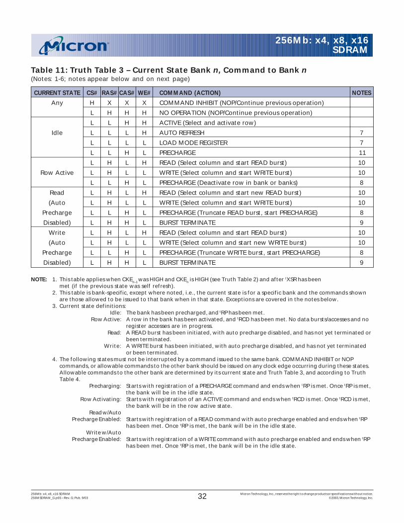
32256Mb: x4, x8, x16 SDRAM Micron Technology, Inc., reserves the right to change products or specifications without notice.256MSDRAM_G.p65 – Rev. G; Pub. 9/03 ©2003, Micron Technology, Inc.
256Mb: x4, x8, x16SDRAM
Table 11: Truth Table 3 – Current State Bank n, Command to Bank n(Notes: 1-6; notes appear below and on next page)
CURRENT STATE CS# RAS# CAS# WE# COMMAND (ACTION) NOTES
Any H X X X COMMAND INHIBIT (NOP/Continue previous operation)
L H H H NO OPERATION (NOP/Continue previous operation)
L L H H ACTIVE (Select and activate row)
Idle L L L H AUTO REFRESH 7
L L L L LOAD MODE REGISTER 7
L L H L PRECHARGE 11
L H L H READ (Select column and start READ burst) 10
Row Active L H L L WRITE (Select column and start WRITE burst) 10
L L H L PRECHARGE (Deactivate row in bank or banks) 8
Read L H L H READ (Select column and start new READ burst) 10
(Auto L H L L WRITE (Select column and start WRITE burst) 10
Precharge L L H L PRECHARGE (Truncate READ burst, start PRECHARGE) 8
Disabled) L H H L BURST TERMINATE 9
Write L H L H READ (Select column and start READ burst) 10
(Auto L H L L WRITE (Select column and start new WRITE burst) 10
Precharge L L H L PRECHARGE (Truncate WRITE burst, start PRECHARGE) 8
Disabled) L H H L BURST TERMINATE 9
NOTE: 1. This table applies when CKEn-1 was HIGH and CKEn is HIGH (see Truth Table 2) and after tXSR has beenmet (if the previous state was self refresh).
2. This table is bank-specific, except where noted, i.e., the current state is for a specific bank and the commands shownare those allowed to be issued to that bank when in that state. Exceptions are covered in the notes below.
3. Current state definitions:Idle: The bank has been precharged, and tRP has been met.
Row Active: A row in the bank has been activated, and tRCD has been met. No data bursts/accesses and noregister accesses are in progress.
Read: A READ burst has been initiated, with auto precharge disabled, and has not yet terminated orbeen terminated.
Write: A WRITE burst has been initiated, with auto precharge disabled, and has not yet terminatedor been terminated.
4. The following states must not be interrupted by a command issued to the same bank. COMMAND INHIBIT or NOPcommands, or allowable commands to the other bank should be issued on any clock edge occurring during these states.Allowable commands to the other bank are determined by its current state and Truth Table 3, and according to TruthTable 4.
Precharging: Starts with registration of a PRECHARGE command and ends when tRP is met. Once tRP is met,the bank will be in the idle state.
Row Activating: Starts with registration of an ACTIVE command and ends when tRCD is met. Once tRCD is met,the bank will be in the row active state.
Read w/AutoPrecharge Enabled: Starts with registration of a READ command with auto precharge enabled and ends when tRP
has been met. Once tRP is met, the bank will be in the idle state.Write w/Auto
Precharge Enabled: Starts with registration of a WRITE command with auto precharge enabled and ends when tRPhas been met. Once tRP is met, the bank will be in the idle state.
33256Mb: x4, x8, x16 SDRAM Micron Technology, Inc., reserves the right to change products or specifications without notice.256MSDRAM_G.p65 – Rev. G; Pub. 9/03 ©2003, Micron Technology, Inc.
256Mb: x4, x8, x16SDRAM
NOTE (continued):5. The following states must not be interrupted by any executable command; COMMAND INHIBIT or NOP commands must
be applied on each positive clock edge during these states.Refreshing: Starts with registration of an AUTO REFRESH command and ends when tRC is met. Once tRC is
met, the SDRAM will be in the all banks idle state.Accessing Mode
Register: Starts with registration of a LOAD MODE REGISTER command and ends when tMRD has beenmet. Once tMRD is met, the SDRAM will be in the all banks idle state.
Precharging All: Starts with registration of a PRECHARGE ALL command and ends when tRP is met. Once tRP ismet, all banks will be in the idle state.
6. All states and sequences not shown are illegal or reserved.7. Not bank-specific; requires that all banks are idle.8. May or may not be bank-specific; if all banks are to be precharged, all must be in a valid state for precharging.9. Not bank-specific; BURST TERMINATE affects the most recent READ or WRITE burst, regardless of bank.
10. READs or WRITEs listed in the Command (Action) column include READs or WRITEs with auto precharge enabled andREADs or WRITEs with auto precharge disabled.
11. Does not affect the state of the bank and acts as a NOP to that bank.
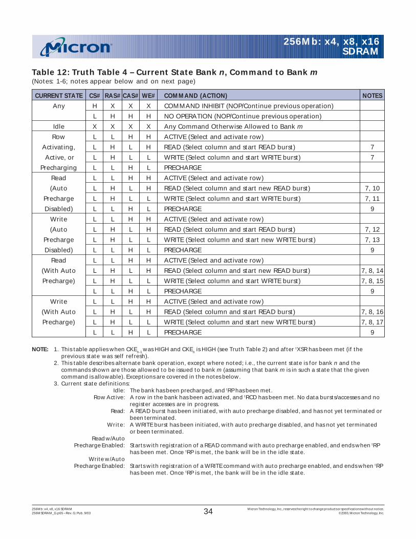
34256Mb: x4, x8, x16 SDRAM Micron Technology, Inc., reserves the right to change products or specifications without notice.256MSDRAM_G.p65 – Rev. G; Pub. 9/03 ©2003, Micron Technology, Inc.
256Mb: x4, x8, x16SDRAM
Table 12: Truth Table 4 – Current State Bank n, Command to Bank m(Notes: 1-6; notes appear below and on next page)
CURRENT STATE CS# RAS# CAS# WE# COMMAND (ACTION) NOTES
Any H X X X COMMAND INHIBIT (NOP/Continue previous operation)
L H H H NO OPERATION (NOP/Continue previous operation)
Idle X X X X Any Command Otherwise Allowed to Bank m
Row L L H H ACTIVE (Select and activate row)
Activating, L H L H READ (Select column and start READ burst) 7
Active, or L H L L WRITE (Select column and start WRITE burst) 7
Precharging L L H L PRECHARGE
Read L L H H ACTIVE (Select and activate row)
(Auto L H L H READ (Select column and start new READ burst) 7, 10
Precharge L H L L WRITE (Select column and start WRITE burst) 7, 11
Disabled) L L H L PRECHARGE 9
Write L L H H ACTIVE (Select and activate row)
(Auto L H L H READ (Select column and start READ burst) 7, 12
Precharge L H L L WRITE (Select column and start new WRITE burst) 7, 13
Disabled) L L H L PRECHARGE 9
Read L L H H ACTIVE (Select and activate row)
(With Auto L H L H READ (Select column and start new READ burst) 7, 8, 14
Precharge) L H L L WRITE (Select column and start WRITE burst) 7, 8, 15
L L H L PRECHARGE 9
Write L L H H ACTIVE (Select and activate row)
(With Auto L H L H READ (Select column and start READ burst) 7, 8, 16
Precharge) L H L L WRITE (Select column and start new WRITE burst) 7, 8, 17
L L H L PRECHARGE 9
NOTE: 1. This table applies when CKEn-1 was HIGH and CKEn is HIGH (see Truth Table 2) and after tXSR has been met (if theprevious state was self refresh).
2. This table describes alternate bank operation, except where noted; i.e., the current state is for bank n and thecommands shown are those allowed to be issued to bank m (assuming that bank m is in such a state that the givencommand is allowable). Exceptions are covered in the notes below.
3. Current state definitions:Idle: The bank has been precharged, and tRP has been met.
Row Active: A row in the bank has been activated, and tRCD has been met. No data bursts/accesses and noregister accesses are in progress.
Read: A READ burst has been initiated, with auto precharge disabled, and has not yet terminated orbeen terminated.
Write: A WRITE burst has been initiated, with auto precharge disabled, and has not yet terminatedor been terminated.
Read w/AutoPrecharge Enabled: Starts with registration of a READ command with auto precharge enabled, and ends when tRP
has been met. Once tRP is met, the bank will be in the idle state.Write w/Auto
Precharge Enabled: Starts with registration of a WRITE command with auto precharge enabled, and ends when tRPhas been met. Once tRP is met, the bank will be in the idle state.
35256Mb: x4, x8, x16 SDRAM Micron Technology, Inc., reserves the right to change products or specifications without notice.256MSDRAM_G.p65 – Rev. G; Pub. 9/03 ©2003, Micron Technology, Inc.
256Mb: x4, x8, x16SDRAM
NOTE (continued):
4. AUTO REFRESH, SELF REFRESH and LOAD MODE REGISTER commands may only be issued when all banks are idle.
5. A BURST TERMINATE command cannot be issued to another bank; it applies to the bank represented by the current stateonly.
6. All states and sequences not shown are illegal or reserved.
7. READs or WRITEs to bank m listed in the Command (Action) column include READs or WRITEs with auto prechargeenabled and READs or WRITEs with auto precharge disabled.
8. CONCURRENT AUTO PRECHARGE: Bank n will initiate the auto precharge command when its burst has been interruptedby bank m’s burst.
9. Burst in bank n continues as initiated.
10. For a READ without auto precharge interrupted by a READ (with or without auto precharge), the READ to bank m willinterrupt the READ on bank n, CAS latency later (Figure 7).
11. For a READ without auto precharge interrupted by a WRITE (with or without auto precharge), the WRITE to bank m willinterrupt the READ on bank n when registered (Figures 9 and 10). DQM should be used one clock prior to the WRITEcommand to prevent bus contention.
12. For a WRITE without auto precharge interrupted by a READ (with or without auto precharge), the READ to bank m willinterrupt the WRITE on bank n when registered (Figure 17), with the data-out appearing CAS latency later. The lastvalid WRITE to bank n will be data-in registered one clock prior to the READ to bank m.
13. For a WRITE without auto precharge interrupted by a WRITE (with or without auto precharge), the WRITE to bank mwill interrupt the WRITE on bank n when registered (Figure 15). The last valid WRITE to bank n will be data-inregistered one clock prior to the READ to bank m.
14. For a READ with auto precharge interrupted by a READ (with or without auto precharge), the READ to bank m willinterrupt the READ on bank n, CAS latency later. The PRECHARGE to bank n will begin when the READ to bank m isregistered (Figure 24).
15. For a READ with auto precharge interrupted by a WRITE (with or without auto precharge), the WRITE to bank m willinterrupt the READ on bank n when registered. DQM should be used two clocks prior to the WRITE command to preventbus contention. The PRECHARGE to bank n will begin when the WRITE to bank m is registered (Figure 25).
16. For a WRITE with auto precharge interrupted by a READ (with or without auto precharge), the READ to bank m willinterrupt the WRITE on bank n when registered, with the data-out appearing CAS latency later. The PRECHARGE to bankn will begin after tWR is met, where tWR begins when the READ to bank m is registered. The last valid WRITE to bank nwill be data-in registered one clock prior to the READ to bank m (Figure 26).
17. For a WRITE with auto precharge interrupted by a WRITE (with or without auto precharge), the WRITE to bank m willinterrupt the WRITE on bank n when registered. The PRECHARGE to bank n will begin after tWR is met, where tWRbegins when the WRITE to bank m is registered. The last valid WRITE to bank n will be data registered one clock priorto the WRITE to bank m (Figure 27).
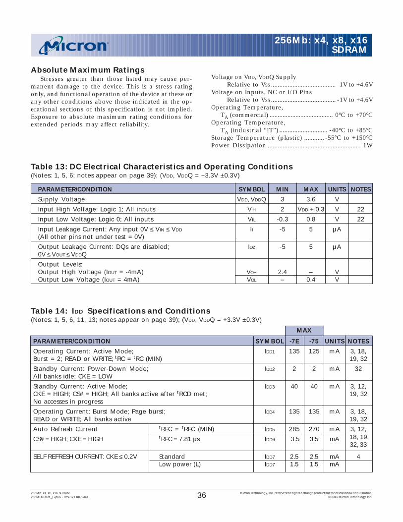
36256Mb: x4, x8, x16 SDRAM Micron Technology, Inc., reserves the right to change products or specifications without notice.256MSDRAM_G.p65 – Rev. G; Pub. 9/03 ©2003, Micron Technology, Inc.
256Mb: x4, x8, x16SDRAM
Table 14: IDD Specifications and Conditions(Notes: 1, 5, 6, 11, 13; notes appear on page 39); (VDD, VDDQ = +3.3V ±0.3V)
PARAMETER/CONDITION SYMBOL -7E -75 UNITS NOTES
Operating Current: Active Mode; IDD1 135 125 mA 3, 18,Burst = 2; READ or WRITE; tRC = tRC (MIN) 19, 32
Standby Current: Power-Down Mode; IDD2 2 2 mA 32All banks idle; CKE = LOW
Standby Current: Active Mode; IDD3 40 40 mA 3, 12,CKE = HIGH; CS# = HIGH; All banks active after tRCD met; 19, 32No accesses in progress
Operating Current: Burst Mode; Page burst; IDD4 135 135 mA 3, 18,READ or WRITE; All banks active 19, 32
Auto Refresh Current tRFC = tRFC (MIN) IDD5 285 270 mA 3, 12,
CS# = HIGH; CKE = HIGH tRFC = 7.81 µs IDD6 3.5 3.5 mA 18, 19,32, 33
SELF REFRESH CURRENT: CKE ≤ 0.2V Standard IDD7 2.5 2.5 mA 4Low power (L) IDD7 1.5 1.5 mA
Absolute Maximum RatingsStresses greater than those listed may cause per-
manent damage to the device. This is a stress ratingonly, and functional operation of the device at these orany other conditions above those indicated in the op-erational sections of this specification is not implied.Exposure to absolute maximum rating conditions forextended periods may affect reliability.
Voltage on VDD, VDDQ SupplyRelative to VSS ....................................... -1V to +4.6V
Voltage on Inputs, NC or I/O PinsRelative to VSS ....................................... -1V to +4.6V
Operating Temperature,TA (commercial) ....................................... 0°C to +70°C
Operating Temperature,TA (industrial “IT”) ............................. -40°C to +85°C
Storage Temperature (plastic) ............ -55°C to +150°CPower Dissipation ........................................................ 1W
Table 13: DC Electrical Characteristics and Operating Conditions(Notes: 1, 5, 6; notes appear on page 39); (VDD, VDDQ = +3.3V ±0.3V)
PARAMETER/CONDITION SYMBOL MIN MAX UNITS NOTES
Supply Voltage VDD, VDDQ 3 3.6 V
Input High Voltage: Logic 1; All inputs VIH 2 VDD + 0.3 V 22
Input Low Voltage: Logic 0; All inputs VIL -0.3 0.8 V 22
Input Leakage Current: Any input 0V ≤ VIN ≤ VDD II -5 5 µA(All other pins not under test = 0V)
Output Leakage Current: DQs are disabled; IOZ -5 5 µA0V ≤ VOUT ≤ VDDQ
Output Levels:Output High Voltage (IOUT = -4mA) VOH 2.4 – VOutput Low Voltage (IOUT = 4mA) VOL – 0.4 V
MAX
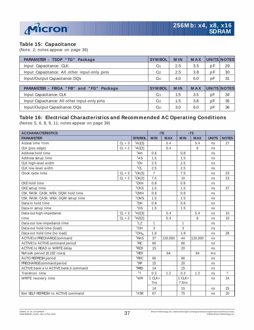
37256Mb: x4, x8, x16 SDRAM Micron Technology, Inc., reserves the right to change products or specifications without notice.256MSDRAM_G.p65 – Rev. G; Pub. 9/03 ©2003, Micron Technology, Inc.
256Mb: x4, x8, x16SDRAM
Table 15: Capacitance(Note: 2; notes appear on page 39)
PARAMETER - TSOP “TG” Package SYMBOL MIN MAX UNITS NOTES
Input Capacitance: CLK CI1 2.5 3.5 pF 29
Input Capacitance: All other input-only pins CI2 2.5 3.8 pF 30
Input/Output Capacitance: DQs CIO 4.0 6.0 pF 31
Table 16: Electrical Characteristics and Recommended AC Operating Conditions(Notes: 5, 6, 8, 9, 11; notes appear on page 39)
AC CHARACTERISTICS -7E -75PARAMETER SYMBOL MIN MAX MIN MAX UNITS NOTESAccess time from CL = 3 tAC(3) 5.4 5.4 ns 27CLK (pos. edge) CL = 2 tAC(2) 5.4 6 nsAddress hold time tAH 0.8 0.8 nsAddress setup time tAS 1.5 1.5 nsCLK high-level width tCH 2.5 2.5 nsCLK low-level width tCL 2.5 2.5 nsClock cycle time CL = 3 tCK(3) 7 7.5 ns 23
CL = 2 tCK(2) 7.5 10 ns 23CKE hold time tCKH 0.8 0.8 nsCKE setup time tCKS 1.5 1.5 ns 37CS#, RAS#, CAS#, WE#, DQM hold time tCMH 0.8 0.8 nsCS#, RAS#, CAS#, WE#, DQM setup time tCMS 1.5 1.5 nsData-in hold time tDH 0.8 0.8 nsData-in setup time tDS 1.5 1.5 nsData-out high-impedance CL = 3 tHZ(3) 5.4 5.4 ns 10time CL = 2 tHZ(2) 5.4 6 ns 10Data-out low-impedance time tLZ 1 1 nsData-out hold time (load) tOH 3 3 nsData-out hold time (no load) tOHN 1.8 1.8 ns 28ACTIVE to PRECHARGE command tRAS 37 120,000 44 120,000 nsACTIVE to ACTIVE command period tRC 60 66 nsACTIVE to READ or WRITE delay tRCD 15 20 nsRefresh period (8,192 rows) tREF 64 64 msAUTO REFRESH period tRFC 66 66 nsPRECHARGE command period tRP 15 20 nsACTIVE bank a to ACTIVE bank b command tRRD 14 15 nsTransition time tT 0.3 1.2 0.3 1.2 ns 7WRITE recovery time tWR 1 CLK+ 1 CLK+ ns 24
7ns 7.5ns
14 15 ns 25Exit SELF REFRESH to ACTIVE command tXSR 67 75 ns 20
PARAMETER - FBGA “FB” and “FG” Package SYMBOL MIN MAX UNITS NOTES
Input Capacitance: CLK CI1 1.5 3.5 pF 34
Input Capacitance: All other input-only pins CI2 1.5 3.8 pF 35
Input/Output Capacitance: DQs CIO 3.0 6.0 pF 36
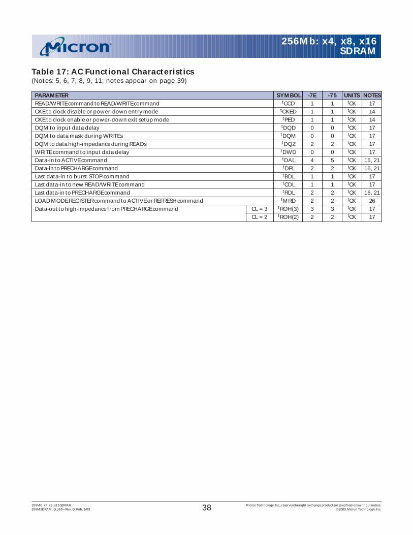
38256Mb: x4, x8, x16 SDRAM Micron Technology, Inc., reserves the right to change products or specifications without notice.256MSDRAM_G.p65 – Rev. G; Pub. 9/03 ©2003, Micron Technology, Inc.
256Mb: x4, x8, x16SDRAM
Table 17: AC Functional Characteristics(Notes: 5, 6, 7, 8, 9, 11; notes appear on page 39)
PARAMETER SYMBOL -7E -75 UNITS NOTESREAD/WRITE command to READ/WRITE command tCCD 1 1 tCK 17CKE to clock disable or power-down entry mode tCKED 1 1 tCK 14CKE to clock enable or power-down exit setup mode tPED 1 1 tCK 14DQM to input data delay tDQD 0 0 tCK 17DQM to data mask during WRITEs tDQM 0 0 tCK 17DQM to data high-impedance during READs tDQZ 2 2 tCK 17WRITE command to input data delay tDWD 0 0 tCK 17Data-in to ACTIVE command tDAL 4 5 tCK 15, 21Data-in to PRECHARGE command tDPL 2 2 tCK 16, 21Last data-in to burst STOP command tBDL 1 1 tCK 17Last data-in to new READ/WRITE command tCDL 1 1 tCK 17Last data-in to PRECHARGE command tRDL 2 2 tCK 16, 21LOAD MODE REGISTER command to ACTIVE or REFRESH command tMRD 2 2 tCK 26Data-out to high-impedance from PRECHARGE command CL = 3 tROH(3) 3 3 tCK 17
CL = 2 tROH(2) 2 2 tCK 17
39256Mb: x4, x8, x16 SDRAM Micron Technology, Inc., reserves the right to change products or specifications without notice.256MSDRAM_G.p65 – Rev. G; Pub. 9/03 ©2003, Micron Technology, Inc.
256Mb: x4, x8, x16SDRAM
15. Timing actually specified by tWR plus tRP; clock(s)specified as a reference only at minimum cycle rate.
16. Timing actually specified by tWR.17. Required clocks are specified by JEDEC function-
ality and are not dependent on any timing param-eter.
18. The IDD current will increase or decrease propor-tionally according to the amount of frequency al-teration for the test condition.
19. Address transitions average one transition everytwo clocks.
20. CLK must be toggled a minimum of two times dur-ing this period.
21.Based on tCK = 7.5ns for -75 and -7E.22. VIH overshoot: VIH (MAX) = VDDQ + 2V for a pulse
width ≤ 3ns, and the pulse width cannot begreater than one third of the cycle rate. VIL under-shoot: VIL (MIN) = -2V for a pulse width ≤ 3ns.
23. The clock frequency must remain constant (stableclock is defined as a signal cycling within timingconstraints specified for the clock pin) during ac-cess or precharge states (READ, WRITE, includingtWR, and PRECHARGE commands). CKE may beused to reduce the data rate.
24. Auto precharge mode only. The precharge timingbudget (tRP) begins 7ns for -7E and 7.5ns for -75after the first clock delay, after the last WRITE isexecuted.
25. Precharge mode only.26. JEDEC and PC100 specify three clocks.27. tAC for -75/-7E at CL = 3 with no load is 4.6ns and is
guaranteed by design.28. Parameter guaranteed by design.29. PC100 specifies a maximum of 4pF.30. PC100 specifies a maximum of 5pF.31. PC100 specifies a maximum of 6.5pF.32. For -75, CL = 3 and tCK = 7.5ns; for -7E, CL = 2 and
tCK = 7.5ns.33. CKE is HIGH during refresh command period
tRFC (MIN) else CKE is LOW. The IDD6 limit is actu-ally a nominal value and does not result in a failvalue.
34. PC133 specifies a minimum of 2.5pF.35. PC133 specifies a minimum of 2.5pF.36. PC133 specifies a minimum of 3.0pF.37. For operating frequencies ≤ 45 MHz tCKS = 3.0ns.
Notes1. All voltages referenced to VSS.2. This parameter is sampled. VDD, VDDQ = +3.3V;
f = 1 MHz, TA = 25°C; pin under test biased at 1.4V.3. IDD is dependent on output loading and cycle rates.
Specified values are obtained with minimum cycletime and the outputs open.
4. Enables on-chip refresh and address counters.5. The minimum specifications are used only to
indicate cycle time at which proper operation overthe full temperature range is ensured; (0°C ≤ TA ≤+70°C for commercial) and (-40°C ≤ TA ≤ +85°Cfor IT).
6. An initial pause of 100µs is required after power-up, followed by two AUTO REFRESH commands,before proper device operation is ensured. (VDD
and VDDQ must be powered up simultaneously. VSS
and VSSQ must be at same potential.) The two AUTOREFRESH command wake-ups should be repeatedany time the tREF refresh requirement is exceeded.
7. AC characteristics assume tT = 1ns.8. In addition to meeting the transition rate specifi-
cation, the clock and CKE must transit between VIH
and VIL (or between VIL and VIH) in a monotonicmanner.
9. Outputs measured at 1.5V with equivalent load:
Q
50pF
10. tHZ defines the time at which the output achievesthe open circuit condition; it is not a reference toVOH or VOL. The last valid data element will meettOH before going High-Z.
11. AC operating and IDD test conditions have VIL = 0Vand VIH = 3.0V using a measurement reference levelof 1.5V. If the input transition time is longer than1ns, then the timing is measured from VIL (MAX)and VIH (MIN) and no longer from the 1.5V mid-point. CLK should always be 1.5V referenced tocrossover. Refer to Micron Technical Note TN-48-09.
12. Other input signals are allowed to transition nomore than once every two clocks and are otherwiseat valid VIH or VIL levels.
13. IDD specifications are tested after the device is prop-erly initialized.
14. Timing actually specified by tCKS; clock(s) speci-fied as a reference only at minimum cycle rate.
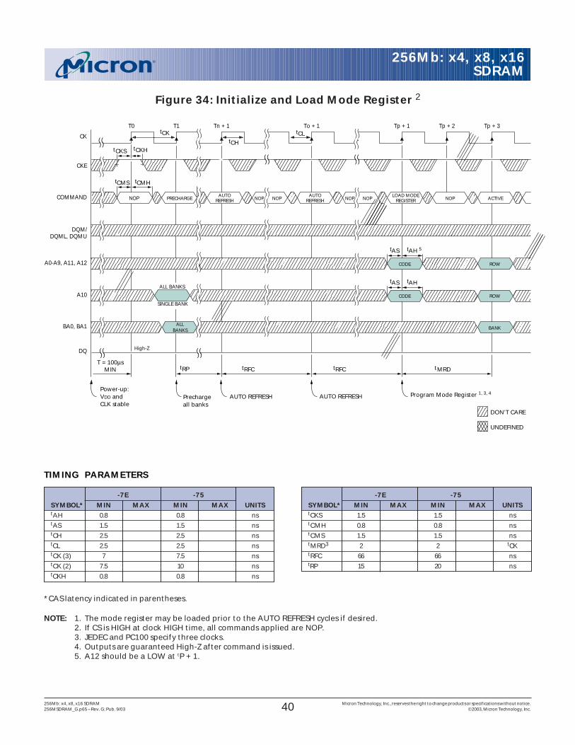
40256Mb: x4, x8, x16 SDRAM Micron Technology, Inc., reserves the right to change products or specifications without notice.256MSDRAM_G.p65 – Rev. G; Pub. 9/03 ©2003, Micron Technology, Inc.
256Mb: x4, x8, x16SDRAM
Figure 34: Initialize and Load Mode Register 2
*CAS latency indicated in parentheses.
NOTE: 1. The mode register may be loaded prior to the AUTO REFRESH cycles if desired.2. If CS is HIGH at clock HIGH time, all commands applied are NOP.3. JEDEC and PC100 specify three clocks.4. Outputs are guaranteed High-Z after command is issued.5. A12 should be a LOW at tP + 1.
-7E -75SYMBOL* MIN MAX MIN MAX UNITStCKS 1.5 1.5 nstCMH 0.8 0.8 nstCMS 1.5 1.5 nstMRD3 2 2 tCKtRFC 66 66 nstRP 15 20 ns
TIMING PARAMETERS
-7E -75SYMBOL* MIN MAX MIN MAX UNITStAH 0.8 0.8 nstAS 1.5 1.5 nstCH 2.5 2.5 nstCL 2.5 2.5 nstCK (3) 7 7.5 nstCK (2) 7.5 10 nstCKH 0.8 0.8 ns
tCH
tCLtCK
CKE
CK
COMMAND
DQ
BA0, BA1 BANK
tRFC tMRD tRFC
AUTO REFRESH AUTO REFRESH Program Mode Register 1, 3, 4
tCMHtCMS
Prechargeall banks
()()
()()
()()
()()
tRP
()()
()()
tCKS
Power-up:VDD andCLK stable
T = 100µsMIN
PRECHARGE NOPAUTO
REFRESH NOPLOAD MODE
REGISTER ACTIVENOP NOPNOP
()()
()()
()()
()()
()()
()()
AUTOREFRESH
ALLBANKS
()()
()()
()()
()()
()()
()()
High-Z
tCKH()()
()()
DQM/DQML, DQMU
()()
()()
()()
()()
()()
()()
()()
()()
()()
()()
()()
()()
()()
()()
()()
()()
()()
NOP
()()
()()
A0-A9, A11, A12 ROW
tAH 5tAS
CODE
()()
()()
()()
()()
()()
()()
()()
()()
A10 ROW
tAHtAS
CODE
()()
()()
()()
()()
ALL BANKS
SINGLE BANK
()()
()()
()()
()()
DON’T CARE
UNDEFINED
T0 T1 Tn + 1 To + 1 Tp + 1 Tp + 2 Tp + 3
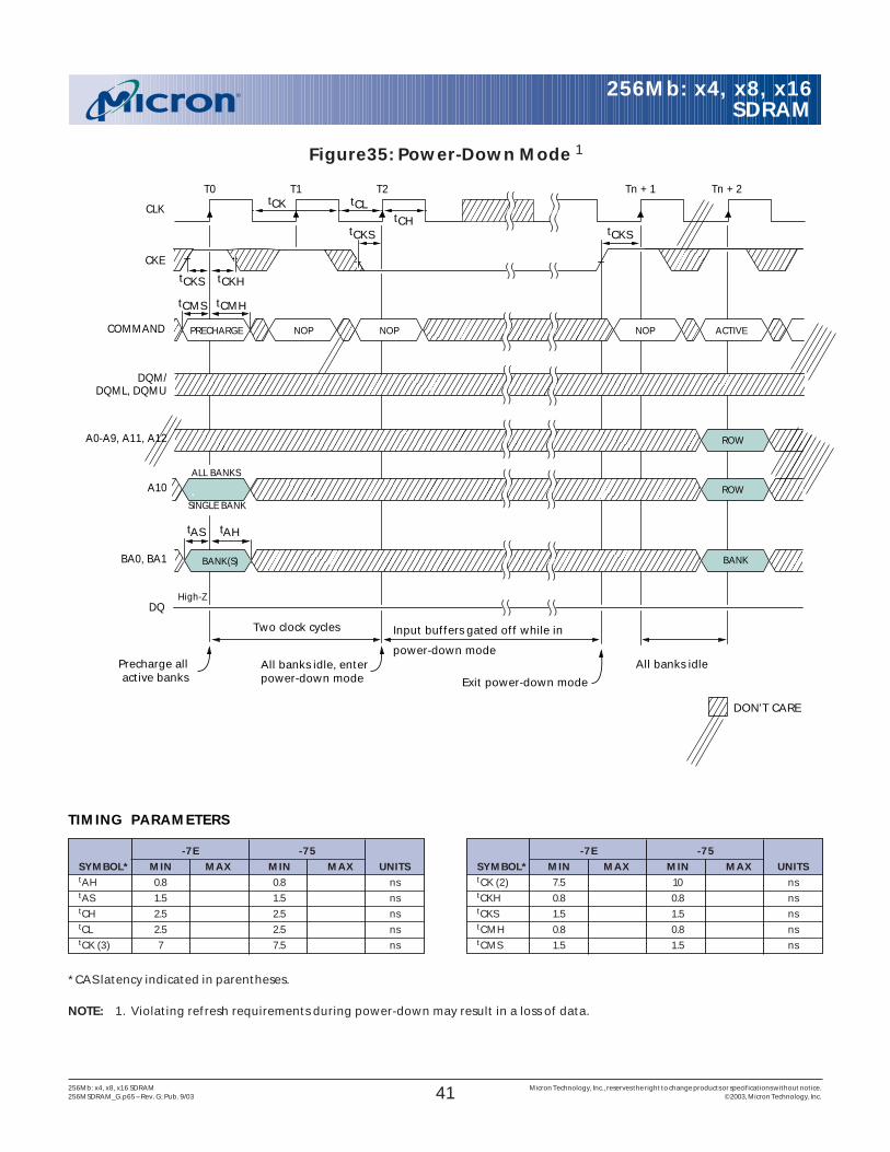
41256Mb: x4, x8, x16 SDRAM Micron Technology, Inc., reserves the right to change products or specifications without notice.256MSDRAM_G.p65 – Rev. G; Pub. 9/03 ©2003, Micron Technology, Inc.
256Mb: x4, x8, x16SDRAM
NOTE: 1. Violating refresh requirements during power-down may result in a loss of data.
Figure35: Power-Down Mode 1
tCH
tCLtCK
Two clock cycles
CKE
CLK
DQ
All banks idle, enter power-down mode
Precharge allactive banks
Input buffers gated off while in
power-down mode
Exit power-down mode
()()
()()
DON’T CARE
tCKS tCKS
COMMAND
tCMHtCMS
PRECHARGE NOP NOP ACTIVENOP
()()
()()
All banks idle
BA0, BA1 BANKBANK(S)
()()
()()
High-Z
tAHtAS
tCKHtCKS
DQM/DQML, DQMU
()()
()()
()()
()()
A0-A9, A11, A12 ROW
()()
()()
ALL BANKS
SINGLE BANK
A10 ROW
()()
()()
T0 T1 T2 Tn + 1 Tn + 2()()
()()
()()
()()
()()
()()
()()
()()
()()
()()
()()
()()
()()
()()
*CAS latency indicated in parentheses.
-7E -75SYMBOL* MIN MAX MIN MAX UNITStCK (2) 7.5 10 nstCKH 0.8 0.8 nstCKS 1.5 1.5 nstCMH 0.8 0.8 nstCMS 1.5 1.5 ns
TIMING PARAMETERS
-7E -75SYMBOL* MIN MAX MIN MAX UNITStAH 0.8 0.8 nstAS 1.5 1.5 nstCH 2.5 2.5 nstCL 2.5 2.5 nstCK (3) 7 7.5 ns
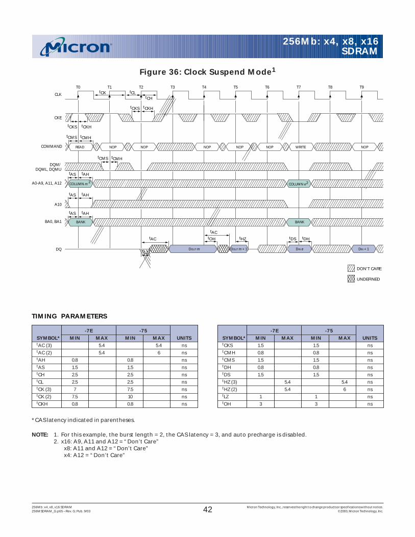
42256Mb: x4, x8, x16 SDRAM Micron Technology, Inc., reserves the right to change products or specifications without notice.256MSDRAM_G.p65 – Rev. G; Pub. 9/03 ©2003, Micron Technology, Inc.
256Mb: x4, x8, x16SDRAM
Figure 36: Clock Suspend Mode1
tCH
tCLtCK
tAC
tLZ
DQM/ DQML, DQMU
CLK
A0-A9, A11, A12
DQ
BA0, BA1
A10
tOH
DOUT m
tAHtAS
tAHtAS
tAHtAS
BANK
tDH
DIN e
tACtHZ
DOUT m + 1
COMMAND
tCMHtCMS
NOPNOP NOP NOPNOPREAD WRITE
DON’T CARE
UNDEFINED
CKE
tCKS tCKH
BANK
COLUMN m
tDS
DIN + 1
NOP
tCKHtCKS
tCMHtCMS
2 COLUMN e2
T0 T1 T2 T3 T4 T5 T6 T7 T8 T9
NOTE: 1. For this example, the burst length = 2, the CAS latency = 3, and auto precharge is disabled.2. x16: A9, A11 and A12 = “Don’t Care”
x8: A11 and A12 = “Don’t Care”x4: A12 = “Don’t Care”
*CAS latency indicated in parentheses.
-7E -75SYMBOL* MIN MAX MIN MAX UNITStCKS 1.5 1.5 nstCMH 0.8 0.8 nstCMS 1.5 1.5 nstDH 0.8 0.8 nstDS 1.5 1.5 nstHZ (3) 5.4 5.4 nstHZ (2) 5.4 6 nstLZ 1 1 nstOH 3 3 ns
TIMING PARAMETERS
-7E -75SYMBOL* MIN MAX MIN MAX UNITStAC (3) 5.4 5.4 nstAC (2) 5.4 6 nstAH 0.8 0.8 nstAS 1.5 1.5 nstCH 2.5 2.5 nstCL 2.5 2.5 nstCK (3) 7 7.5 nstCK (2) 7.5 10 nstCKH 0.8 0.8 ns
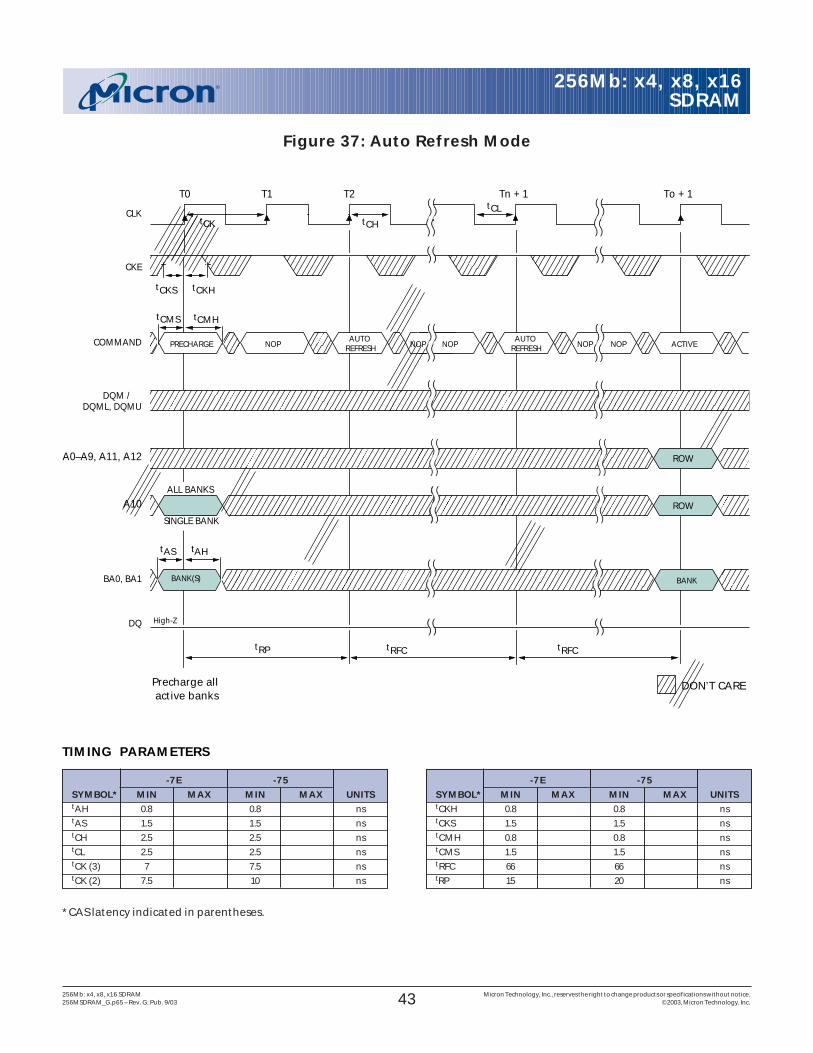
43256Mb: x4, x8, x16 SDRAM Micron Technology, Inc., reserves the right to change products or specifications without notice.256MSDRAM_G.p65 – Rev. G; Pub. 9/03 ©2003, Micron Technology, Inc.
256Mb: x4, x8, x16SDRAM
Figure 37: Auto Refresh Mode
*CAS latency indicated in parentheses.
-7E -75SYMBOL* MIN MAX MIN MAX UNITStCKH 0.8 0.8 nstCKS 1.5 1.5 nstCMH 0.8 0.8 nstCMS 1.5 1.5 nstRFC 66 66 nstRP 15 20 ns
TIMING PARAMETERS
-7E -75SYMBOL* MIN MAX MIN MAX UNITStAH 0.8 0.8 nstAS 1.5 1.5 nstCH 2.5 2.5 nstCL 2.5 2.5 nstCK (3) 7 7.5 nstCK (2) 7.5 10 ns
tCH
tCLtCK
CKE
CLK
DQ
tRFC RFC
()()
()()
()()
tRP
()()
()()
()()
()()
COMMAND
tCMHtCMS
NOPNOP
()()
()()
BANK
ACTIVEAUTO
REFRESH
()()
()()
NOPNOPPRECHARGE
Precharge all active banks
AUTO REFRESH
t
High-Z
BA0, BA1 BANK(S)
()()
()()
()()
()()
tAHtAS
tCKHtCKS
()()
NOP
()()
()()
()()
()()
DQM / DQML, DQMU
A0–A9, A11, A12 ROW
()()
()()
ALL BANKS
SINGLE BANK
A10 ROW
()()
()()
()()
()()
()()
()()
()()
()()
DON’T CARE
T0 T1 T2 Tn + 1 To + 1
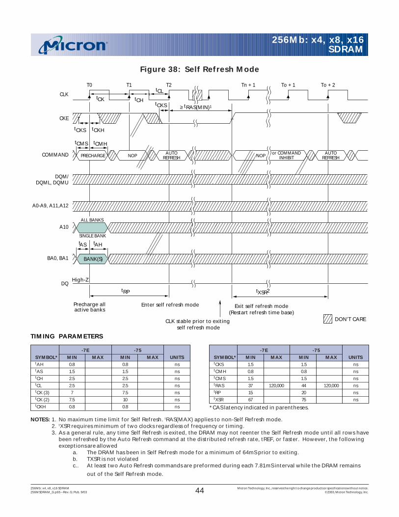
44256Mb: x4, x8, x16 SDRAM Micron Technology, Inc., reserves the right to change products or specifications without notice.256MSDRAM_G.p65 – Rev. G; Pub. 9/03 ©2003, Micron Technology, Inc.
256Mb: x4, x8, x16SDRAM
Figure 38: Self Refresh Mode
*CAS latency indicated in parentheses.
-7E -75SYMBOL* MIN MAX MIN MAX UNITStCKS 1.5 1.5 nstCMH 0.8 0.8 nstCMS 1.5 1.5 nstRAS 37 120,000 44 120,000 nstRP 15 20 nstXSR 67 75 ns
TIMING PARAMETERS
-7E -75SYMBOL* MIN MAX MIN MAX UNITStAH 0.8 0.8 nstAS 1.5 1.5 nstCH 2.5 2.5 nstCL 2.5 2.5 nstCK (3) 7 7.5 nstCK (2) 7.5 10 nstCKH 0.8 0.8 ns
tCH
tCLtCK
tRP
CKE
CLK
DQ
Enter self refresh modePrecharge allactive banks
t 2XSR
CLK stable prior to exiting self refresh mode
Exit self refresh mode(Restart refresh time base)
()()
()()
()()
()()
()()
DON’T CARE
COMMAND
tCMHtCMS
AUTOREFRESHPRECHARGE NOP NOP or COMMAND
INHIBIT
()()
()()
()()
()()
BA0, BA1 BANK(S)
()()
()()
High-Z
tCKS
AHAS
AUTOREFRESH
tRAS(MIN)1()()
()()
()()
()()
tCKHtCKS
DQM/DQML, DQMU
()()
()()
()()
()()
tt
A0-A9, A11,A12()()
()()
()()
()()
ALL BANKS
SINGLE BANK
A10()()
()()
()()
()()
()()
()()
T0 T1 T2 Tn + 1 To + 1 To + 2()()
()()
≥
NOTES: 1. No maximum time limit for Self Refresh. tRAS(MAX) applies to non-Self Refresh mode.2. tXSR requires minimum of two clocks regardless of frequency or timing.3. As a general rule, any time Self Refresh is exited, the DRAM may not reenter the Self Refresh mode until all rows have
been refreshed by the Auto Refresh command at the distributed refresh rate, tREF, or faster. However, the followingexceptions are allowed
a. The DRAM has been in Self Refresh mode for a minimum of 64mS prior to exiting.b. TXSR is not violatedc.. At least two Auto Refresh commands are preformed during each 7.81mS interval while the DRAM remains
out of the Self Refresh mode.
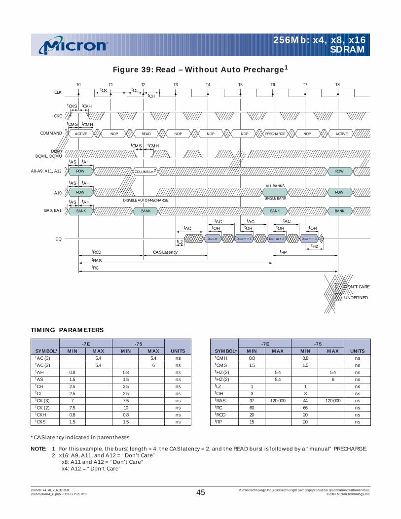
45256Mb: x4, x8, x16 SDRAM Micron Technology, Inc., reserves the right to change products or specifications without notice.256MSDRAM_G.p65 – Rev. G; Pub. 9/03 ©2003, Micron Technology, Inc.
256Mb: x4, x8, x16SDRAM
Figure 39: Read – Without Auto Precharge1
ALL BANKS
tCH
tCLtCK
tAC
tLZ
tRP
tRAS
tRCD CAS Latency
tRC
DQM/DQML, DQMU
CKE
CLK
A0-A9, A11, A12
DQ
BA0, BA1
A10
tOH
DOUT m
tCMHtCMS
tAHtAS
tAHtAS
tAHtAS
ROW
ROW
BANK BANK BANK
ROW
ROW
BANK
tHZ
tOH
DOUT m + 3
tACtOH
tACtOH
tAC
DOUT m + 2DOUT m + 1
COMMAND
tCMHtCMS
PRECHARGENOPNOP NOPACTIVE NOP READ NOP ACTIVE
DISABLE AUTO PRECHARGE SINGLE BANK
DON’T CARE
UNDEFINED
tCKHtCKS
COLUMN m2
T0 T1 T2 T4T3 T5 T6 T7 T8
NOTE: 1. For this example, the burst length = 4, the CAS latency = 2, and the READ burst is followed by a “manual” PRECHARGE.2. x16: A9, A11, and A12 = “Don’t Care”
x8: A11 and A12 = “Don’t Care”x4: A12 = “Don’t Care”
*CAS latency indicated in parentheses.
-7E -75SYMBOL* MIN MAX MIN MAX UNITStCMH 0.8 0.8 nstCMS 1.5 1.5 nstHZ (3) 5.4 5.4 nstHZ (2) 5.4 6 nstLZ 1 1 nstOH 3 3 nstRAS 37 120,000 44 120,000 nstRC 60 66 nstRCD 20 20 nstRP 15 20 ns
TIMING PARAMETERS
-7E -75SYMBOL* MIN MAX MIN MAX UNITStAC (3) 5.4 5.4 nstAC (2) 5.4 6 nstAH 0.8 0.8 nstAS 1.5 1.5 nstCH 2.5 2.5 nstCL 2.5 2.5 nstCK (3) 7 7.5 nstCK (2) 7.5 10 nstCKH 0.8 0.8 nstCKS 1.5 1.5 ns
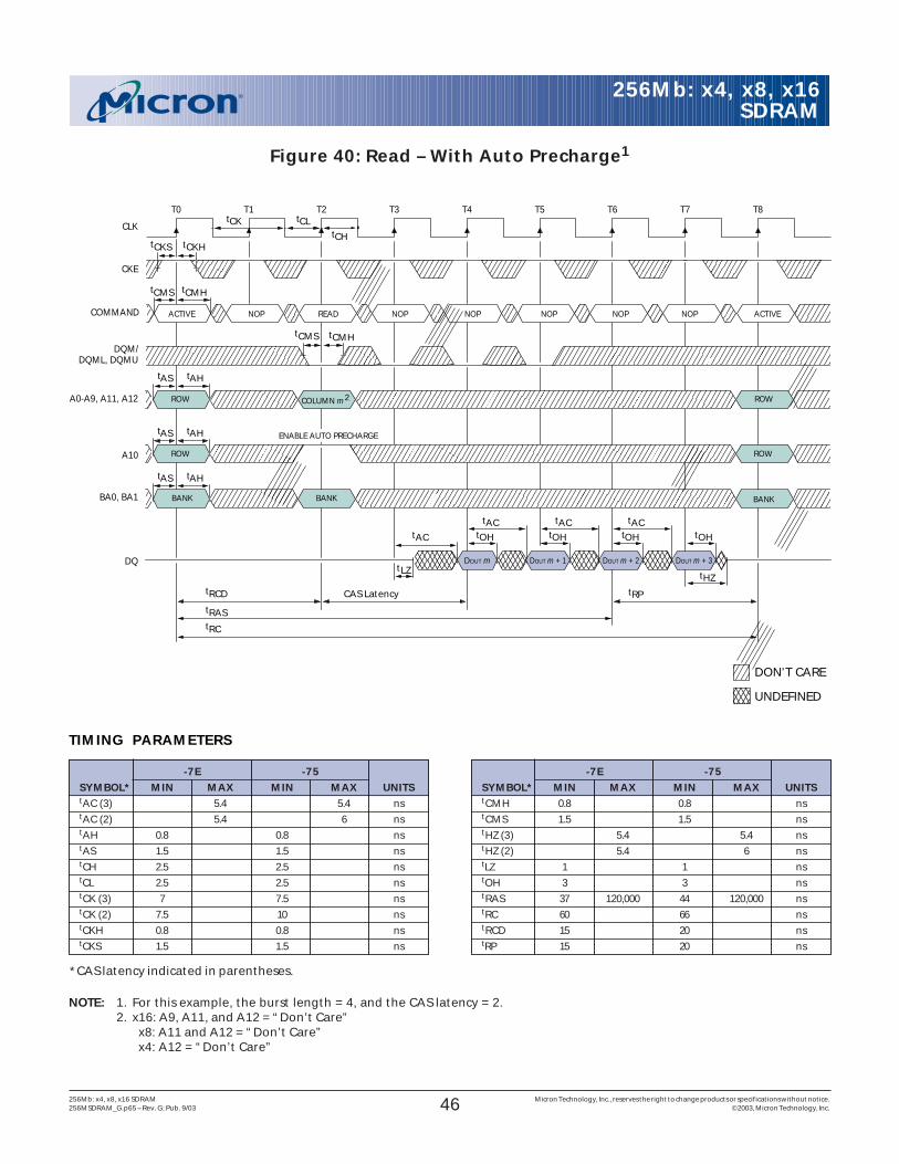
46256Mb: x4, x8, x16 SDRAM Micron Technology, Inc., reserves the right to change products or specifications without notice.256MSDRAM_G.p65 – Rev. G; Pub. 9/03 ©2003, Micron Technology, Inc.
256Mb: x4, x8, x16SDRAM
Figure 40: Read – With Auto Precharge1
ENABLE AUTO PRECHARGE
tCH
tCLtCK
tAC
tLZ
tRP
tRAS
tRCD CAS Latency
tRC
DQM/DQML, DQMU
CKE
CLK
A0-A9, A11, A12
DQ
BA0, BA1
A10
tOH
DOUT m
tCMHtCMS
tAHtAS
tAHtAS
tAHtAS
ROW
ROW
BANK BANK
ROW
ROW
BANK
DON’T CARE
UNDEFINED
tHZ
tOH
DOUT m + 3
tACtOH
tACtOH
tAC
DOUT m + 2DOUT m + 1
COMMAND
tCMHtCMS
NOPNOP NOPACTIVE NOP READ NOP ACTIVENOP
tCKHtCKS
COLUMN m2
T0 T1 T2 T4T3 T5 T6 T7 T8
NOTE: 1. For this example, the burst length = 4, and the CAS latency = 2.2. x16: A9, A11, and A12 = “Don’t Care”
x8: A11 and A12 = “Don’t Care”x4: A12 = “Don’t Care”
*CAS latency indicated in parentheses.
-7E -75SYMBOL* MIN MAX MIN MAX UNITStCMH 0.8 0.8 nstCMS 1.5 1.5 nstHZ (3) 5.4 5.4 nstHZ (2) 5.4 6 nstLZ 1 1 nstOH 3 3 nstRAS 37 120,000 44 120,000 nstRC 60 66 nstRCD 15 20 nstRP 15 20 ns
TIMING PARAMETERS
-7E -75SYMBOL* MIN MAX MIN MAX UNITStAC (3) 5.4 5.4 nstAC (2) 5.4 6 nstAH 0.8 0.8 nstAS 1.5 1.5 nstCH 2.5 2.5 nstCL 2.5 2.5 nstCK (3) 7 7.5 nstCK (2) 7.5 10 nstCKH 0.8 0.8 nstCKS 1.5 1.5 ns
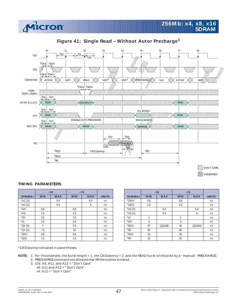
47256Mb: x4, x8, x16 SDRAM Micron Technology, Inc., reserves the right to change products or specifications without notice.256MSDRAM_G.p65 – Rev. G; Pub. 9/03 ©2003, Micron Technology, Inc.
256Mb: x4, x8, x16SDRAM
Figure 41: Single Read – Without Autor Precharge1
TIMING PARAMETERS
-7E -75SYMBOL* MIN MAX MIN MAX UNITStAC (3) 5.4 5.4 nstAC (2) 5.4 6 nstAH 0.8 0.8 nstAS 1.5 1.5 nstCH 2.5 2.5 nstCL 2.5 2.5 nstCK (3) 7 7.5 nstCK (2) 7.5 10 nstCKH 0.8 0.8 nstCKS 1.5 1.5 ns
tCMH 0.8 0.8 nstCMS 1.5 1.5 nstHZ (3) 5.4 5.4 nstHZ (2) 5.4 6 nstLZ 1 1 nstOH 3 3 nstRAS 37 120,000 44 120,000 nstRC 60 66 nstRCD 15 20 nstRP 15 20 ns
*CAS latency indicated in parentheses.
-7E -75SYMBOL* MIN MAX MIN MAX UNITS
NOTE: 1. For this example, the burst length = 1, the CAS latency = 2, and the READ burst is followed by a “manual” PRECHARGE.2. PRECHARGE command not allowed else tRAS would be violated.3. x16: A9, A11, and A12 = “Don’t Care”
x8: A11 and A12 = “Don’t Care”x4: A12 = “Don’t Care”
ALL BANKS
tCH
tCLtCK
tAC
tLZ
tRP
tRAS
tRCD CAS Latency
tRC
tOH
DOUT m
tCMHtCMS
tAHtAS
tAHtAS
tAHtAS
ROW
ROW
BANK BANK(S) BANK
ROW
ROW
BANK
tHZ
tCMHtCMS
NOPNOPNOP PRECHARGEACTIVE NOP READ ACTIVE NOP
DISABLE AUTO PRECHARGE SINGLE BANKS
DON’T CARE
UNDEFINED
COLUMN m3
tCKHtCKS
T0 T1 T2 T3 T4 T5 T6 T7 T8
DQM / DQML, DQMU
CKE
CLK
A0-A9, A11,A12
DQ
BA0, BA1
A10
COMMAND 2 2
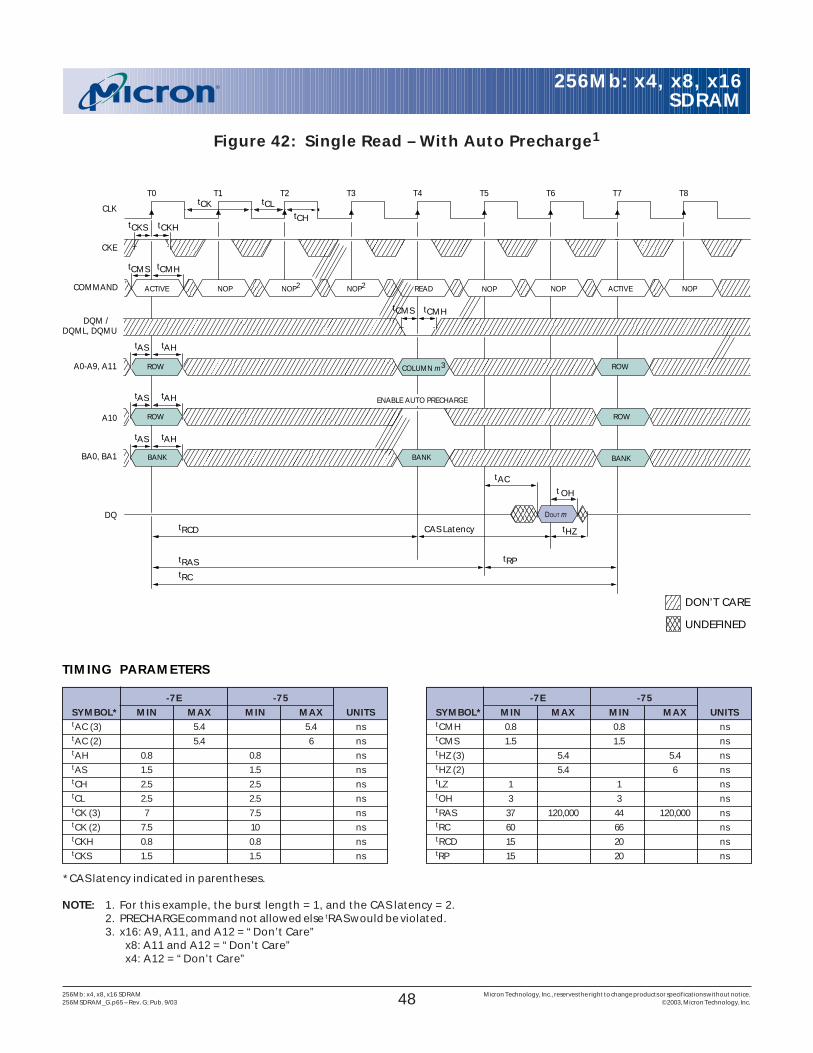
48256Mb: x4, x8, x16 SDRAM Micron Technology, Inc., reserves the right to change products or specifications without notice.256MSDRAM_G.p65 – Rev. G; Pub. 9/03 ©2003, Micron Technology, Inc.
256Mb: x4, x8, x16SDRAM
NOTE: 1. For this example, the burst length = 1, and the CAS latency = 2.2. PRECHARGE command not allowed else tRAS would be violated.3. x16: A9, A11, and A12 = “Don’t Care”
x8: A11 and A12 = “Don’t Care”x4: A12 = “Don’t Care”
*CAS latency indicated in parentheses.
-7E -75SYMBOL* MIN MAX MIN MAX UNITStCMH 0.8 0.8 nstCMS 1.5 1.5 nstHZ (3) 5.4 5.4 nstHZ (2) 5.4 6 nstLZ 1 1 nstOH 3 3 nstRAS 37 120,000 44 120,000 nstRC 60 66 nstRCD 15 20 nstRP 15 20 ns
TIMING PARAMETERS
-7E -75SYMBOL* MIN MAX MIN MAX UNITStAC (3) 5.4 5.4 nstAC (2) 5.4 6 nstAH 0.8 0.8 nstAS 1.5 1.5 nstCH 2.5 2.5 nstCL 2.5 2.5 nstCK (3) 7 7.5 nstCK (2) 7.5 10 nstCKH 0.8 0.8 nstCKS 1.5 1.5 ns
Figure 42: Single Read – With Auto Precharge1
ENABLE AUTO PRECHARGE
tCH
tCLtCK
tRPtRAS
tRCD CAS Latency
tRC
DQM / DQML, DQMU
CKE
CLK
A0-A9, A11
DQ
BA0, BA1
A10
tCMHtCMS
tAHtAS
tAHtAS
tAHtAS
ROW
ROW
BANK BANK
ROW
ROW
BANK
DON’T CARE
UNDEFINED
tHZ
tOH
DOUT m
tAC
COMMAND
tCMHtCMS
NOP2 READACTIVE NOP NOP2 ACTIVENOP
tCKHtCKS
COLUMN m3
T0 T1 T2 T4T3 T5 T6 T7 T8
NOP NOP
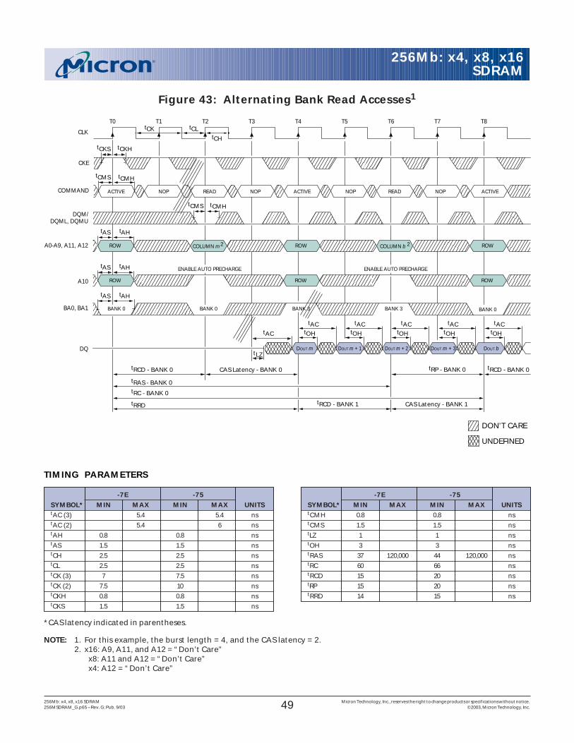
49256Mb: x4, x8, x16 SDRAM Micron Technology, Inc., reserves the right to change products or specifications without notice.256MSDRAM_G.p65 – Rev. G; Pub. 9/03 ©2003, Micron Technology, Inc.
256Mb: x4, x8, x16SDRAM
Figure 43: Alternating Bank Read Accesses1
ENABLE AUTO PRECHARGE
tCH
tCLtCK
tAC
tLZ
DQM/DQML, DQMU
CLK
A0-A9, A11, A12
DQ
BA0, BA1
A10
tOH
DOUT m
tCMHtCMS
tAHtAS
tAHtAS
tAHtAS
ROW
ROW
ROW
ROW
DON’T CARE
UNDEFINED
tOH
DOUT m + 3
tACtOH
tACtOH
tAC
DOUT m + 2DOUT m + 1
COMMAND
tCMHtCMS
NOP NOPACTIVE NOP READ NOP ACTIVE
tOH
DOUT b
tAC tAC
READ
ENABLE AUTO PRECHARGE
ROW
ACTIVE
ROW
BANK 0 BANK 0 BANK 3 BANK 3 BANK 0
CKE
tCKHtCKS
COLUMN m2 COLUMN b 2
T0 T1 T2 T4T3 T5 T6 T7 T8
tRP - BANK 0
tRAS - BANK 0
tRCD - BANK 0 tRCD - BANK 0CAS Latency - BANK 0
tRCD - BANK 1 CAS Latency - BANK 1
t
t
RC - BANK 0
RRD
NOTE: 1. For this example, the burst length = 4, and the CAS latency = 2.2. x16: A9, A11, and A12 = “Don’t Care”
x8: A11 and A12 = “Don’t Care”x4: A12 = “Don’t Care”
*CAS latency indicated in parentheses.
-7E -75SYMBOL* MIN MAX MIN MAX UNITStCMH 0.8 0.8 nstCMS 1.5 1.5 nstLZ 1 1 nstOH 3 3 nstRAS 37 120,000 44 120,000 nstRC 60 66 nstRCD 15 20 nstRP 15 20 nstRRD 14 15 ns
TIMING PARAMETERS
-7E -75SYMBOL* MIN MAX MIN MAX UNITStAC (3) 5.4 5.4 nstAC (2) 5.4 6 nstAH 0.8 0.8 nstAS 1.5 1.5 nstCH 2.5 2.5 nstCL 2.5 2.5 nstCK (3) 7 7.5 nstCK (2) 7.5 10 nstCKH 0.8 0.8 nstCKS 1.5 1.5 ns
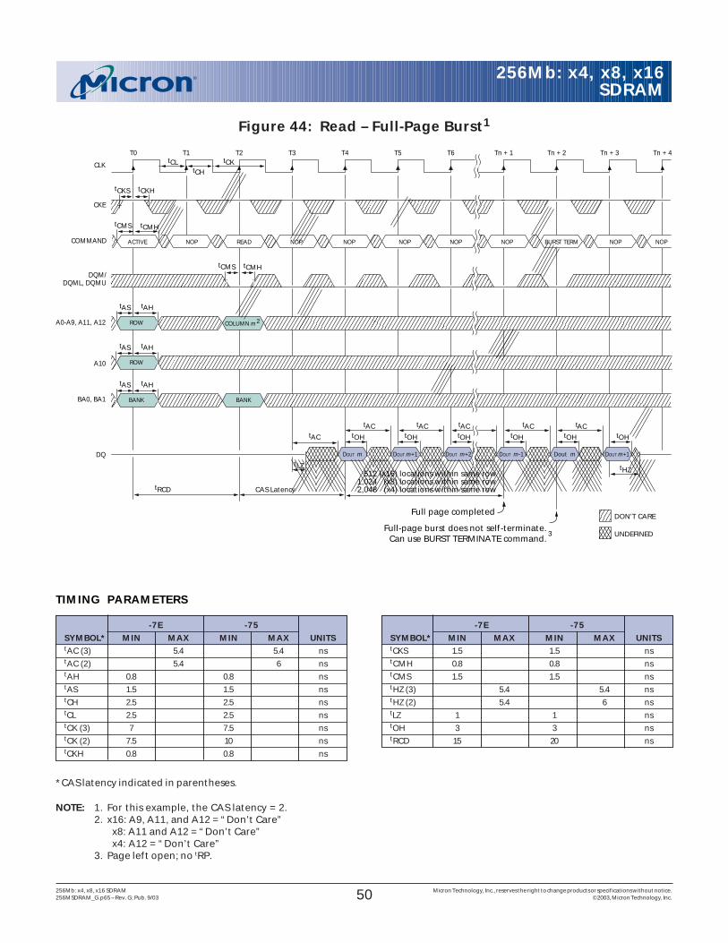
50256Mb: x4, x8, x16 SDRAM Micron Technology, Inc., reserves the right to change products or specifications without notice.256MSDRAM_G.p65 – Rev. G; Pub. 9/03 ©2003, Micron Technology, Inc.
256Mb: x4, x8, x16SDRAM
Figure 44: Read – Full-Page Burst1
tCH
tCL tCK
tAC
tLZ
tRCD CAS Latency
DQM/DQML, DQMU
CKE
CLK
A0-A9, A11, A12
DQ
BA0, BA1
A10
tOH
DOUT m
tCMHtCMS
tAHtAS
tAHtAS
tACtOH
DOUT m+1
ROW
ROW
tHZ
tACtOH
DOUT m+1
tACtOH
DOUT m+2
tACtOH
DOUT m-1
tACtOH
Dout m
Full-page burst does not self-terminate.Can use BURST TERMINATE command.
()()
()()
()()
()()
()()
()()
()()
Full page completed
512 (x16) locations within same row1,024 (x8) locations within same row2,048 (x4) locations within same row
DON’T CARE
UNDEFINED
COMMAND
tCMHtCMS
NOPNOP NOPACTIVE NOP READ NOP BURST TERMNOP NOP
()()
()()
NOP
()()
()()
tAHtAS
BANK
()()
()()
BANK
tCKHtCKS()()
()()
()()
()()
COLUMN m2
3
T0 T1 T2 T4T3 T5 T6 Tn + 1 Tn + 2 Tn + 3 Tn + 4
NOTE: 1. For this example, the CAS latency = 2.2. x16: A9, A11, and A12 = “Don’t Care”
x8: A11 and A12 = “Don’t Care”x4: A12 = “Don’t Care”
3. Page left open; no tRP.
*CAS latency indicated in parentheses.
-7E -75SYMBOL* MIN MAX MIN MAX UNITStCKS 1.5 1.5 nstCMH 0.8 0.8 nstCMS 1.5 1.5 nstHZ (3) 5.4 5.4 nstHZ (2) 5.4 6 nstLZ 1 1 nstOH 3 3 nstRCD 15 20 ns
TIMING PARAMETERS
-7E -75SYMBOL* MIN MAX MIN MAX UNITStAC (3) 5.4 5.4 nstAC (2) 5.4 6 nstAH 0.8 0.8 nstAS 1.5 1.5 nstCH 2.5 2.5 nstCL 2.5 2.5 nstCK (3) 7 7.5 nstCK (2) 7.5 10 nstCKH 0.8 0.8 ns
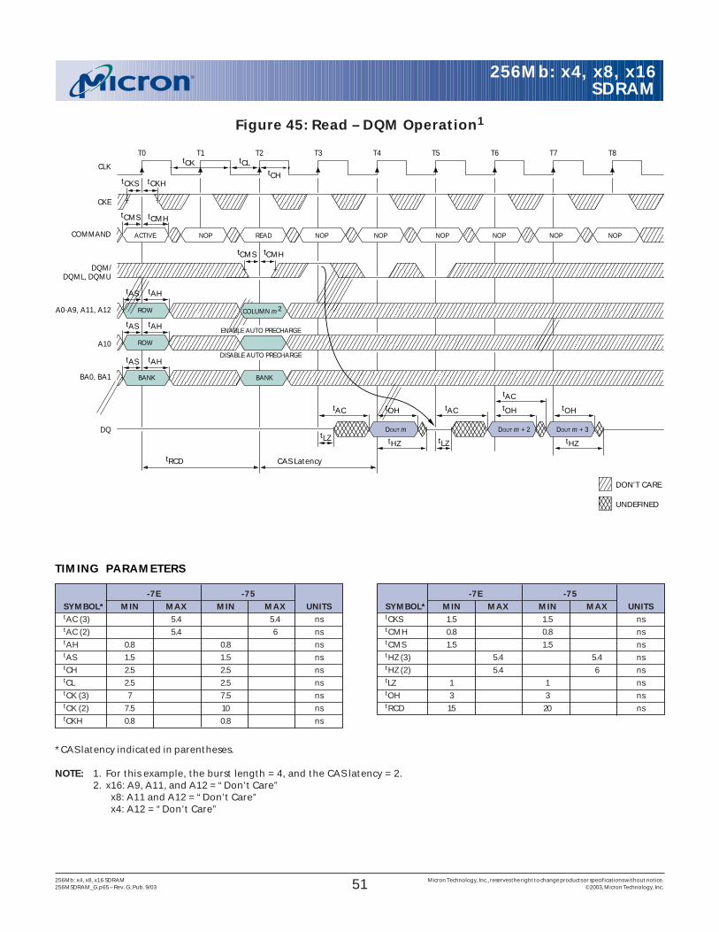
51256Mb: x4, x8, x16 SDRAM Micron Technology, Inc., reserves the right to change products or specifications without notice.256MSDRAM_G.p65 – Rev. G; Pub. 9/03 ©2003, Micron Technology, Inc.
256Mb: x4, x8, x16SDRAM
Figure 45: Read – DQM Operation1
tCH
tCLtCK
tRCD CAS Latency
DQM/DQML, DQMU
CKE
CLK
A0-A9, A11, A12
DQ
BA0, BA1
A10
tCMS
ROW
BANK
ROW
BANK
DON’T CARE
UNDEFINED
tAC
LZDOUT m
tOH
DOUT m + 3DOUT m + 2t
tHZ LZt
tCMH
COMMAND NOPNOP NOPACTIVE NOP READ NOPNOP NOP
tHZ
tAC tOH
tACtOH
tAHtAS
tCMS tCMH
tAHtAS
tAHtAS
tCKHtCKS
ENABLE AUTO PRECHARGE
DISABLE AUTO PRECHARGE
COLUMN m2
T0 T1 T2 T4T3 T5 T6 T7 T8
NOTE: 1. For this example, the burst length = 4, and the CAS latency = 2.2. x16: A9, A11, and A12 = “Don’t Care”
x8: A11 and A12 = “Don’t Care”x4: A12 = “Don’t Care”
*CAS latency indicated in parentheses.
-7E -75SYMBOL* MIN MAX MIN MAX UNITStCKS 1.5 1.5 nstCMH 0.8 0.8 nstCMS 1.5 1.5 nstHZ (3) 5.4 5.4 nstHZ (2) 5.4 6 nstLZ 1 1 nstOH 3 3 nstRCD 15 20 ns
TIMING PARAMETERS
-7E -75SYMBOL* MIN MAX MIN MAX UNITStAC (3) 5.4 5.4 nstAC (2) 5.4 6 nstAH 0.8 0.8 nstAS 1.5 1.5 nstCH 2.5 2.5 nstCL 2.5 2.5 nstCK (3) 7 7.5 nstCK (2) 7.5 10 nstCKH 0.8 0.8 ns
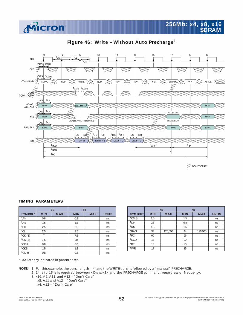
52256Mb: x4, x8, x16 SDRAM Micron Technology, Inc., reserves the right to change products or specifications without notice.256MSDRAM_G.p65 – Rev. G; Pub. 9/03 ©2003, Micron Technology, Inc.
256Mb: x4, x8, x16SDRAM
Figure 46: Write – Without Auto Precharge1
NOTE: 1. For this example, the burst length = 4, and the WRITE burst is followed by a “manual” PRECHARGE.2. 14ns to 15ns is required between <DIN m+3> and the PRECHARGE command, regardless of frequency.3. x16: A9, A11, and A12 = “Don’t Care”
x8: A11 and A12 = “Don’t Care”x4: A12 = “Don’t Care”
*CAS latency indicated in parentheses.
-7E -75SYMBOL* MIN MAX MIN MAX UNITStCMS 1.5 1.5 nstDH 0.8 0.8 nstDS 1.5 1.5 nstRAS 37 120,000 44 120,000 nstRC 60 66 nstRCD 15 20 nstRP 15 20 nstWR 14 15 ns
TIMING PARAMETERS
-7E -75SYMBOL* MIN MAX MIN MAX UNITStAH 0.8 0.8 nstAS 1.5 1.5 nstCH 2.5 2.5 nstCL 2.5 2.5 nstCK (3) 7 7.5 nstCK (2) 7.5 10 nstCKH 0.8 0.8 nstCKS 1.5 1.5 nstCMH 0.8 0.8 ns
DISABLE AUTO PRECHARGE
tCH
tCLtCK
tRPtRAS
tRCD
tRC
DQM/DQML, DQMU
CKE
CLK
A0–A9,A11, A12
DQ
BA0, BA1
A10
tCMHtCMS
tAHtAS
ROW
BANK BANK
ROW
BANK
t
DON’T CARE
DIN m
tDHtDS
DIN m + 1 DIN m + 2 DIN m + 3
COMMAND
tCMHtCMS
NOPNOP NOPACTIVE NOP WRITE PRECHARGE
tAHtAS
tAHtAS
tDHtDS tDHtDS tDHtDS
SINGLE BANK
tCKHtCKS
COLUMN m2
3
T0 T1 T2 T4T3 T5 T6 T7 T8 T9
ROW
BANK
ROW
ACTIVENOP
WR
NOP
ALL BANKs
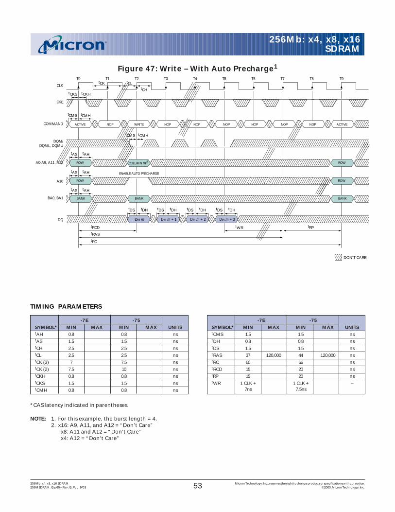
53256Mb: x4, x8, x16 SDRAM Micron Technology, Inc., reserves the right to change products or specifications without notice.256MSDRAM_G.p65 – Rev. G; Pub. 9/03 ©2003, Micron Technology, Inc.
256Mb: x4, x8, x16SDRAM
Figure 47: Write – With Auto Precharge1
NOTE: 1. For this example, the burst length = 4.2. x16: A9, A11, and A12 = “Don’t Care”
x8: A11 and A12 = “Don’t Care”x4: A12 = “Don’t Care”
*CAS latency indicated in parentheses.
-7E -75SYMBOL* MIN MAX MIN MAX UNITStCMS 1.5 1.5 nstDH 0.8 0.8 nstDS 1.5 1.5 nstRAS 37 120,000 44 120,000 nstRC 60 66 nstRCD 15 20 nstRP 15 20 nstWR 1 CLK + 1 CLK + –
7ns 7.5ns
TIMING PARAMETERS
-7E -75SYMBOL* MIN MAX MIN MAX UNITStAH 0.8 0.8 nstAS 1.5 1.5 nstCH 2.5 2.5 nstCL 2.5 2.5 nstCK (3) 7 7.5 nstCK (2) 7.5 10 nstCKH 0.8 0.8 nstCKS 1.5 1.5 nstCMH 0.8 0.8 ns
ENABLE AUTO PRECHARGE
tCH
tCLtCK
tRPtRAS
tRCD
tRC
DQM/DQML, DQMU
CKE
CLK
A0-A9, A11, A12
DQ
BA0, BA1
A10
tCMHtCMS
tAHtAS
ROW
ROW
BANK BANK
ROW
ROW
BANK
tWR
DON’T CARE
DIN m
tDHtDS
DIN m + 1 DIN m + 2 DIN m + 3
COMMAND
tCMHtCMS
NOPNOP NOPACTIVE NOP WRITE NOP ACTIVE
tAHtAS
tAHtAS
tDHtDS tDHtDS tDHtDS
tCKHtCKS
NOP NOP
COLUMN m2
T0 T1 T2 T4T3 T5 T6 T7 T8 T9
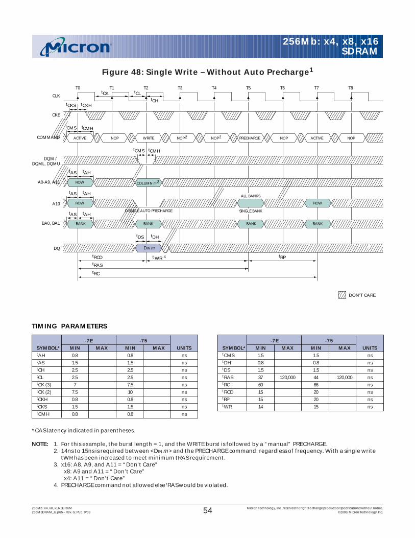
54256Mb: x4, x8, x16 SDRAM Micron Technology, Inc., reserves the right to change products or specifications without notice.256MSDRAM_G.p65 – Rev. G; Pub. 9/03 ©2003, Micron Technology, Inc.
256Mb: x4, x8, x16SDRAM
Figure 48: Single Write – Without Auto Precharge1
TIMING PARAMETERS
-7E -75SYMBOL* MIN MAX MIN MAX UNITStAH 0.8 0.8 nstAS 1.5 1.5 nstCH 2.5 2.5 nstCL 2.5 2.5 nstCK (3) 7 7.5 nstCK (2) 7.5 10 nstCKH 0.8 0.8 nstCKS 1.5 1.5 nstCMH 0.8 0.8 ns
tCMS 1.5 1.5 nstDH 0.8 0.8 nstDS 1.5 1.5 nstRAS 37 120,000 44 120,000 nstRC 60 66 nstRCD 15 20 nstRP 15 20 nstWR 14 15 ns
*CAS latency indicated in parentheses.
DISABLE AUTO PRECHARGE
ALL BANKS
tCH
tCLtCK
tRPtRAS
tRCD
tRC
DQM / DQML, DQMU
CKE
CLK
A0-A9, A11
DQ
BA0, BA1
A10
tCMHtCMS
tAHtAS
ROW
BANK BANK BANK
ROW
ROW
BANK
tWR
DIN m
tDHtDS
COMMAND
tCMHtCMS
NOP 2NOP 2 PRECHARGEACTIVE NOP WRITE ACTIVENOP NOP
tAHtAS
tAHtAS
SINGLE BANK
tCKHtCKS
COLUMN m3
4
T0 T1 T2 T4T3 T5 T6 T7 T8
DON’T CARE
-7E -75SYMBOL* MIN MAX MIN MAX UNITS
NOTE: 1. For this example, the burst length = 1, and the WRITE burst is followed by a “manual” PRECHARGE.2. 14ns to 15ns is required between <DIN m> and the PRECHARGE command, regardless of frequency. With a single write
tWR has been increased to meet minimum tRAS requirement.3. x16: A8, A9, and A11 = “Don’t Care”
x8: A9 and A11 = “Don’t Care”x4: A11 = “Don’t Care”
4. PRECHARGE command not allowed else tRAS would be violated.
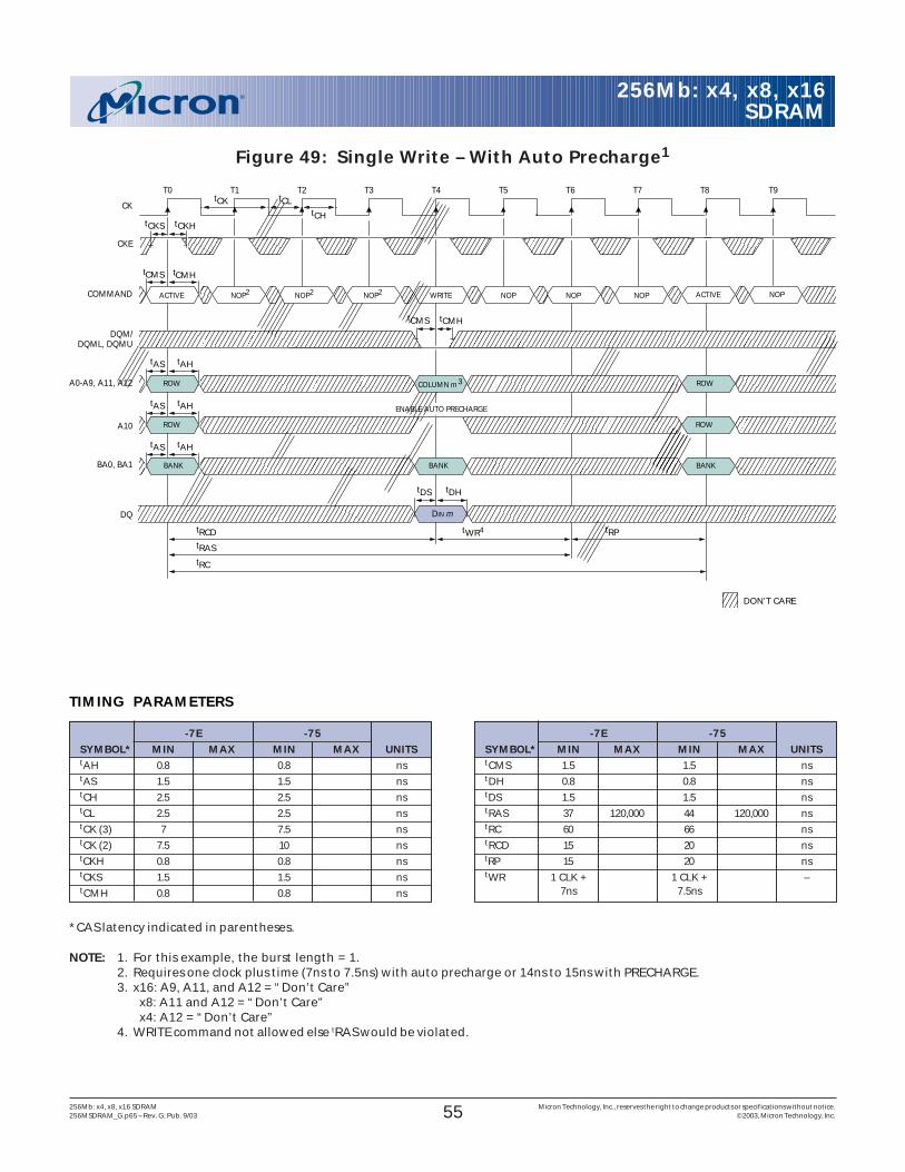
55256Mb: x4, x8, x16 SDRAM Micron Technology, Inc., reserves the right to change products or specifications without notice.256MSDRAM_G.p65 – Rev. G; Pub. 9/03 ©2003, Micron Technology, Inc.
256Mb: x4, x8, x16SDRAM
Figure 49: Single Write – With Auto Precharge1
NOTE: 1. For this example, the burst length = 1.2. Requires one clock plus time (7ns to 7.5ns) with auto precharge or 14ns to 15ns with PRECHARGE.3. x16: A9, A11, and A12 = “Don’t Care”
x8: A11 and A12 = “Don’t Care”x4: A12 = “Don’t Care”
4. WRITE command not allowed else tRAS would be violated.
*CAS latency indicated in parentheses.
-7E -75SYMBOL* MIN MAX MIN MAX UNITStCMS 1.5 1.5 nstDH 0.8 0.8 nstDS 1.5 1.5 nstRAS 37 120,000 44 120,000 nstRC 60 66 nstRCD 15 20 nstRP 15 20 nstWR 1 CLK + 1 CLK + –
7ns 7.5ns
TIMING PARAMETERS
-7E -75SYMBOL* MIN MAX MIN MAX UNITStAH 0.8 0.8 nstAS 1.5 1.5 nstCH 2.5 2.5 nstCL 2.5 2.5 nstCK (3) 7 7.5 nstCK (2) 7.5 10 nstCKH 0.8 0.8 nstCKS 1.5 1.5 nstCMH 0.8 0.8 ns
ENABLE AUTO PRECHARGE
tCH
tCLtCK
tRPtRAS
tRCD
tRC
DQM/DQML, DQMU
CKE
CK
A0-A9, A11, A12
DQ
BA0, BA1
A10
tCMHtCMS
tAHtAS
ROW
ROW
BANK BANK
ROW
ROW
BANK
tWR4
DIN m
COMMAND
tCMHtCMS
NOP2 NOP2 NOPACTIVE NOP2 WRITE NOPACTIVE
tAHtAS
tAHtAS
tDHtDS
tCKHtCKS
NOP NOP
COLUMN m3
T0 T1 T2 T4T3 T5 T6 T7 T8 T9
DON’T CARE
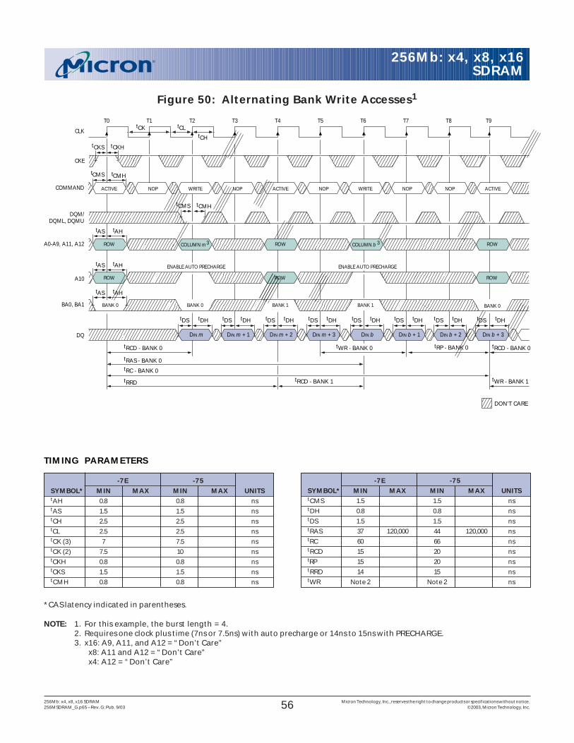
56256Mb: x4, x8, x16 SDRAM Micron Technology, Inc., reserves the right to change products or specifications without notice.256MSDRAM_G.p65 – Rev. G; Pub. 9/03 ©2003, Micron Technology, Inc.
256Mb: x4, x8, x16SDRAM
Figure 50: Alternating Bank Write Accesses1
tCH
tCLtCKCLK
DQ
DON’T CARE
DIN m
tDHtDS
DIN m + 1 DIN m + 2 DIN m + 3
COMMAND
tCMHtCMS
NOP NOPACTIVE NOP WRITE NOP NOP ACTIVE
tDHtDS tDHtDS tDHtDS
ACTIVE WRITE
DIN b
tDHtDS
DIN b + 1 DIN b + 3
tDHtDS tDHtDS
ENABLE AUTO PRECHARGE
DQM/DQML, DQMU
A0-A9, A11, A12
BA0, BA1
A10
tCMHtCMS
tAHtAS
tAHtAS
tAHtAS
ROW
ROW
ROW
ROW
ENABLE AUTO PRECHARGE
ROW
ROW
BANK 0 BANK 0 BANK 1 BANK 0 BANK 1
CKE
tCKHtCKS
DIN b + 2
tDHtDS
COLUMN b 3COLUMN m3
tRP - BANK 0
tRAS - BANK 0
tRCD - BANK 0 t
t
RCD - BANK 0tWR - BANK 0
WR - BANK 1tRCD - BANK 1
t
t
RC - BANK 0
RRD
T0 T1 T2 T3 T4 T5 T6 T7 T8 T9
NOTE: 1. For this example, the burst length = 4.2. Requires one clock plus time (7ns or 7.5ns) with auto precharge or 14ns to 15ns with PRECHARGE.3. x16: A9, A11, and A12 = “Don’t Care”
x8: A11 and A12 = “Don’t Care”x4: A12 = “Don’t Care”
*CAS latency indicated in parentheses.
-7E -75SYMBOL* MIN MAX MIN MAX UNITStCMS 1.5 1.5 nstDH 0.8 0.8 nstDS 1.5 1.5 nstRAS 37 120,000 44 120,000 nstRC 60 66 nstRCD 15 20 nstRP 15 20 nstRRD 14 15 nstWR Note 2 Note 2 ns
TIMING PARAMETERS
-7E -75SYMBOL* MIN MAX MIN MAX UNITStAH 0.8 0.8 nstAS 1.5 1.5 nstCH 2.5 2.5 nstCL 2.5 2.5 nstCK (3) 7 7.5 nstCK (2) 7.5 10 nstCKH 0.8 0.8 nstCKS 1.5 1.5 nstCMH 0.8 0.8 ns
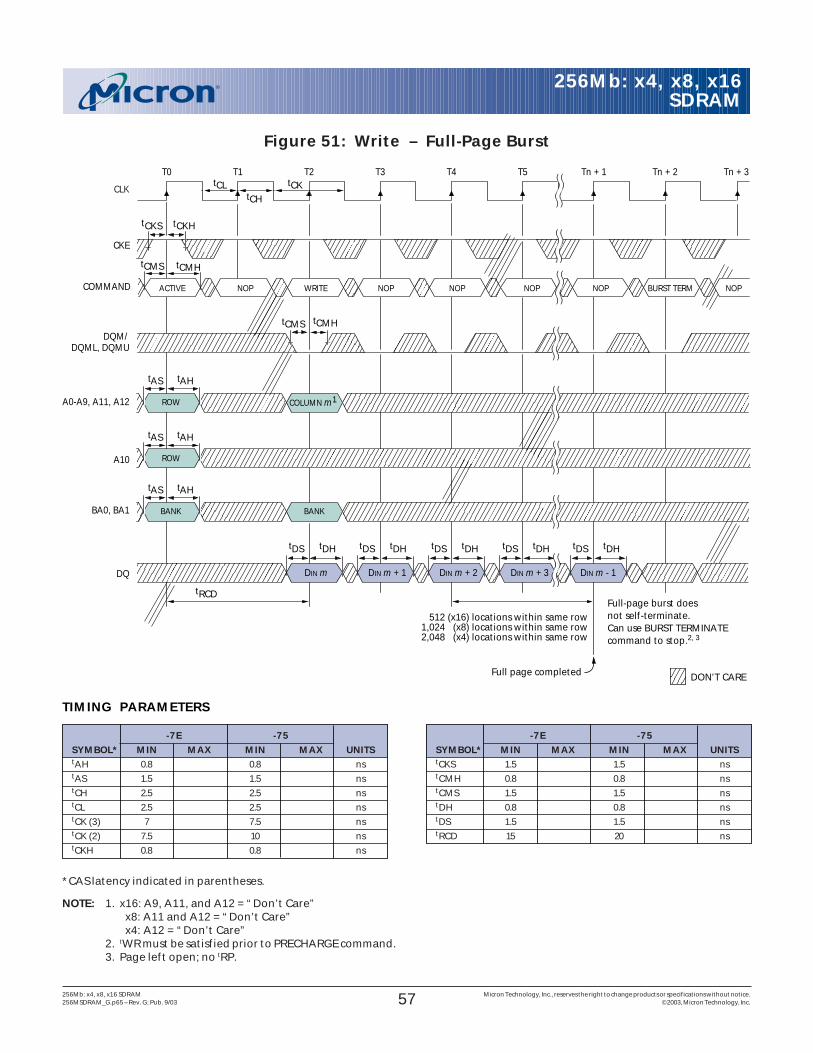
57256Mb: x4, x8, x16 SDRAM Micron Technology, Inc., reserves the right to change products or specifications without notice.256MSDRAM_G.p65 – Rev. G; Pub. 9/03 ©2003, Micron Technology, Inc.
256Mb: x4, x8, x16SDRAM
Figure 51: Write – Full-Page Burst
tCH
tCL tCK
tRCD
DQM/ DQML, DQMU
CKE
CLK
A0-A9, A11, A12
BA0, BA1
A10
tCMS
tAHtAS
tAHtAS
ROW
ROW
Full-page burst doesnot self-terminate. Can use BURST TERMINATE command to stop.2, 3
()()
()()
()()
()()
Full page completed DON’T CARE
COMMAND
tCMHtCMS
NOPNOP NOPACTIVE NOP WRITE BURST TERMNOP NOP
()()
()()
()()
()()
DQ DIN m
tDHtDS
DIN m + 1 DIN m + 2 DIN m + 3
tDHtDS tDHtDS tDHtDS
DIN m - 1
tDHtDS
tAHtAS
BANK
()()
()()
BANK
tCMH
tCKHtCKS
()()
()()
()()
()()
()()
()()
512 (x16) locations within same row1,024 (x8) locations within same row2,048 (x4) locations within same row
COLUMN m1
T0 T1 T2 T3 T4 T5 Tn + 1 Tn + 2 Tn + 3
NOTE: 1. x16: A9, A11, and A12 = “Don’t Care”x8: A11 and A12 = “Don’t Care”x4: A12 = “Don’t Care”
2. tWR must be satisfied prior to PRECHARGE command.3. Page left open; no tRP.
*CAS latency indicated in parentheses.
-7E -75SYMBOL* MIN MAX MIN MAX UNITStCKS 1.5 1.5 nstCMH 0.8 0.8 nstCMS 1.5 1.5 nstDH 0.8 0.8 nstDS 1.5 1.5 nstRCD 15 20 ns
TIMING PARAMETERS
-7E -75SYMBOL* MIN MAX MIN MAX UNITStAH 0.8 0.8 nstAS 1.5 1.5 nstCH 2.5 2.5 nstCL 2.5 2.5 nstCK (3) 7 7.5 nstCK (2) 7.5 10 nstCKH 0.8 0.8 ns
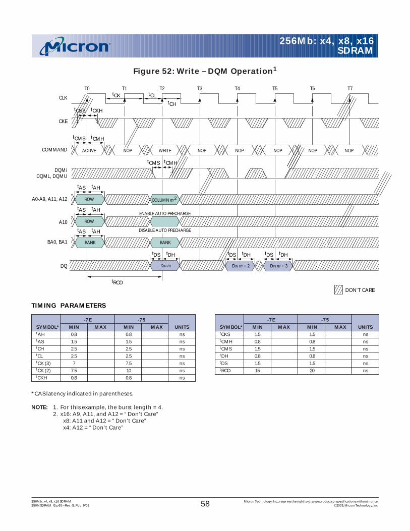
58256Mb: x4, x8, x16 SDRAM Micron Technology, Inc., reserves the right to change products or specifications without notice.256MSDRAM_G.p65 – Rev. G; Pub. 9/03 ©2003, Micron Technology, Inc.
256Mb: x4, x8, x16SDRAM
Figure 52: Write – DQM Operation1
tCH
tCLtCK
tRCD
DQM/DQML, DQMU
CKE
CLK
A0-A9, A11, A12
DQ
BA0, BA1
A10
tCMS
tAHtAS
ROW
BANK
ROW
BANK
ENABLE AUTO PRECHARGE
DIN m + 3
tDHtDS
DIN m DIN m + 2
tCMH
COMMAND NOPNOP NOPACTIVE NOP WRITE NOPNOP
DON’T CARE
tCMS tCMH
tDHtDStDHtDS
tAHtAS
tAHtAS
DISABLE AUTO PRECHARGE
tCKHtCKS
COLUMN m2
T0 T1 T2 T3 T4 T5 T6 T7
NOTE: 1. For this example, the burst length = 4.2. x16: A9, A11, and A12 = “Don’t Care”
x8: A11 and A12 = “Don’t Care”x4: A12 = “Don’t Care”
*CAS latency indicated in parentheses.
-7E -75SYMBOL* MIN MAX MIN MAX UNITStCKS 1.5 1.5 nstCMH 0.8 0.8 nstCMS 1.5 1.5 nstDH 0.8 0.8 nstDS 1.5 1.5 nstRCD 15 20 ns
TIMING PARAMETERS
-7E -75SYMBOL* MIN MAX MIN MAX UNITStAH 0.8 0.8 nstAS 1.5 1.5 nstCH 2.5 2.5 nstCL 2.5 2.5 nstCK (3) 7 7.5 nstCK (2) 7.5 10 nstCKH 0.8 0.8 ns
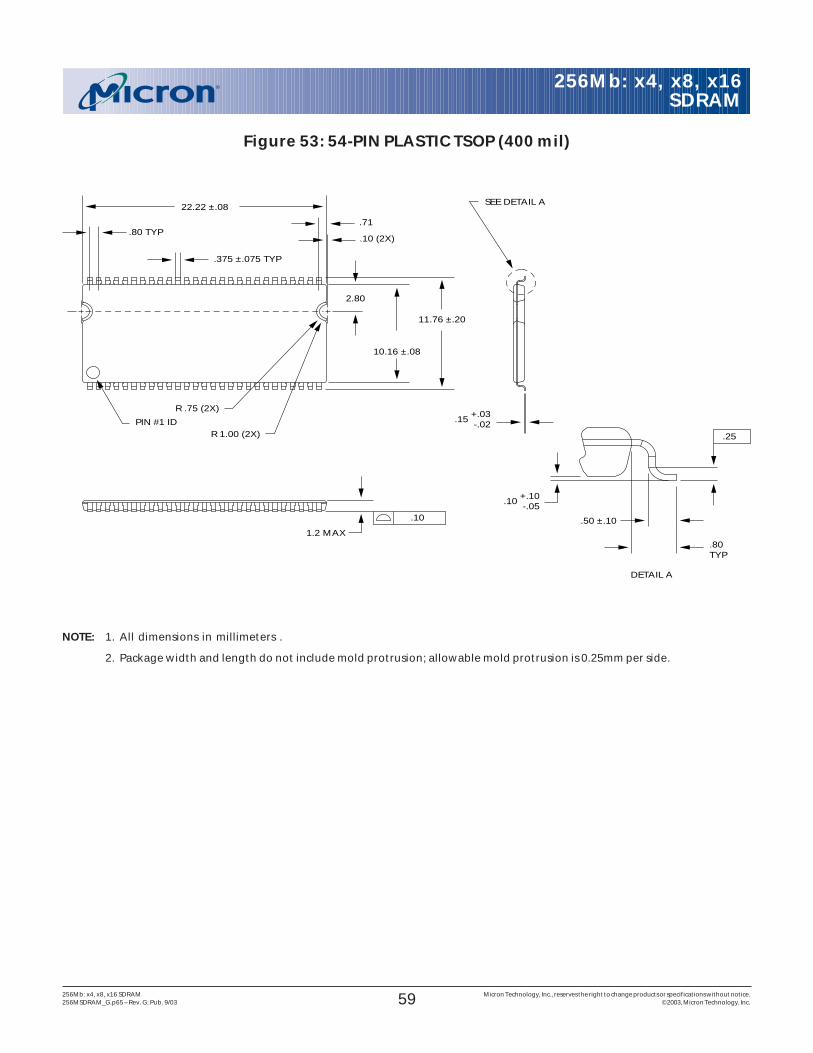
59256Mb: x4, x8, x16 SDRAM Micron Technology, Inc., reserves the right to change products or specifications without notice.256MSDRAM_G.p65 – Rev. G; Pub. 9/03 ©2003, Micron Technology, Inc.
256Mb: x4, x8, x16SDRAM
Figure 53: 54-PIN PLASTIC TSOP (400 mil)
NOTE: 1. All dimensions in millimeters .
2. Package width and length do not include mold protrusion; allowable mold protrusion is 0.25mm per side.
SEE DETAIL A
.10 +.10-.05
.15 +.03-.02
R 1.00 (2X)
R .75 (2X)
.80 TYP.71
11.76 ±.20
10.16 ±.08
.50 ±.10
PIN #1 ID
DETAIL A
22.22 ±.08
.375 ±.075 TYP
1.2 MAX
.10
.25
.80TYP
.10 (2X)
2.80
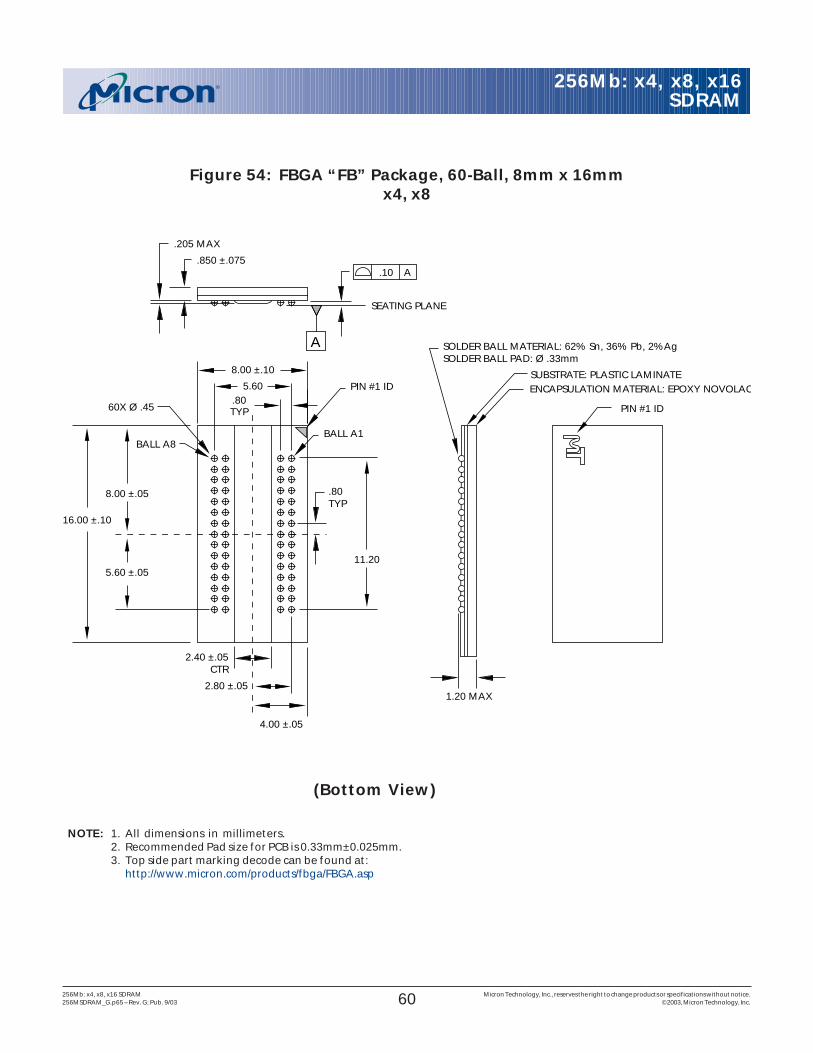
60256Mb: x4, x8, x16 SDRAM Micron Technology, Inc., reserves the right to change products or specifications without notice.256MSDRAM_G.p65 – Rev. G; Pub. 9/03 ©2003, Micron Technology, Inc.
256Mb: x4, x8, x16SDRAM
Figure 54: FBGA “FB” Package, 60-Ball, 8mm x 16mmx4, x8
(Bottom View)
NOTE: 1. All dimensions in millimeters.2. Recommended Pad size for PCB is 0.33mm±0.025mm.3. Top side part marking decode can be found at:
http://www.micron.com/products/fbga/FBGA.asp
PIN #1 ID
SUBSTRATE: PLASTIC LAMINATEENCAPSULATION MATERIAL: EPOXY NOVOLAC
SOLDER BALL MATERIAL: 62% Sn, 36% Pb, 2%AgSOLDER BALL PAD: Ø .33mm
SEATING PLANE
.850 ±.075
.205 MAX
.10 A
A
.80TYP
16.00 ±.10
11.20
1.20 MAX
5.60 ±.05
8.00 ±.05
PIN #1 ID
BALL A1BALL A8
.80TYP
4.00 ±.05
2.80 ±.05
2.40 ±.05CTR
8.00 ±.10
5.60
60X Ø .45
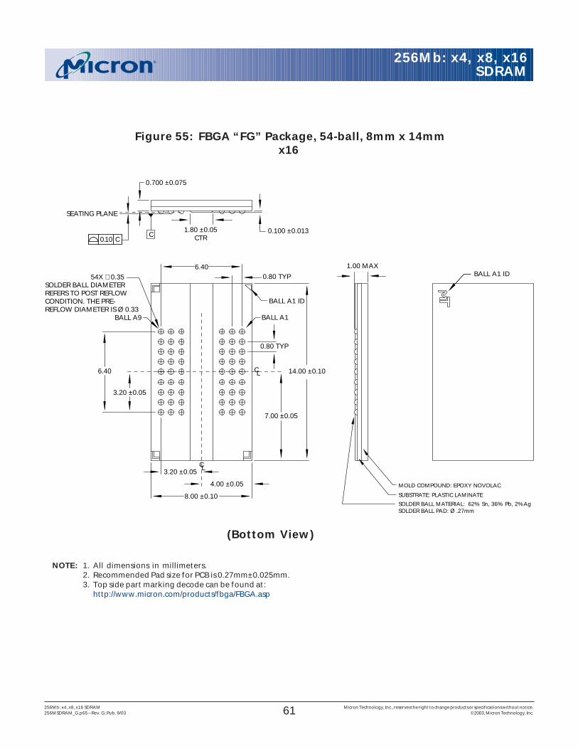
61256Mb: x4, x8, x16 SDRAM Micron Technology, Inc., reserves the right to change products or specifications without notice.256MSDRAM_G.p65 – Rev. G; Pub. 9/03 ©2003, Micron Technology, Inc.
256Mb: x4, x8, x16SDRAM
Figure 55: FBGA “FG” Package, 54-ball, 8mm x 14mmx16
BALL A1 ID1.00 MAX
MOLD COMPOUND: EPOXY NOVOLAC
SUBSTRATE: PLASTIC LAMINATE
SOLDER BALL MATERIAL: 62% Sn, 36% Pb, 2%AgSOLDER BALL PAD: Ø .27mm
14.00 ±0.10
BALL A1BALL A9
BALL A1 ID
0.80 TYP
0.80 TYP
1.80 ±0.05CTR
7.00 ±0.05
8.00 ±0.10
4.00 ±0.05
3.20 ±0.05
3.20 ±0.05
0.700 ±0.075
0.100 ±0.013
SEATING PLANE
C
6.40
6.40
0.10 C
54X ∅ 0.35SOLDER BALL DIAMETER REFERS TO POST REFLOW CONDITION. THE PRE-REFLOW DIAMETER IS Ø 0.33
C L
C L
(Bottom View)
NOTE: 1. All dimensions in millimeters.2. Recommended Pad size for PCB is 0.27mm±0.025mm.3. Top side part marking decode can be found at:
http://www.micron.com/products/fbga/FBGA.asp