Embed Size (px)
Citation preview
SUPPORTING INFORMATION
Enhanced TiO2/MAPbI3 Electronic Coupling by
Interface Modification with PbI2
EdoardoMosconi,aGiulia Grancini,b CristinaRoldán-Carmona,b Paul Gratia,b Iwan Zimmermann,b
Mohammad Khaja Nazeeruddinb,*, FilippoDeAngelis a,*
aComputationalLaboratoryforHybrid/OrganicPhotovoltaics(CLHYO),CNR-ISTM, Via Elce di Sotto
8, I-06123,Perugia,Italy
b Group for Molecular Engineering of Functional Materials, Institute of Chemical Sciences and
Engineering, Ecolepolytechniquefédérale de Lausanne, CH-1951 Sion, Switzerland
E-mail: [email protected]; [email protected]
Computational Details
Geometry optimizations have been carried out at PBE-GGA1 level with SIESTA 3.0 program
package2 using a DZ basis set along with non-relativistic pseudo-potentials for Ti, O, C, N and H
atoms. Pb atoms are treated with the WC-GGA3 relativistic pseudo-potential. Electrons from O, N
and C 2s, 2p; H 1s; Ti 4s, 3d; Pb 6s, 6p, 5d shells explicitly included in the calculations. Spin orbit
interactions are not included in SIESTA calculations. A value of 100 Ry is used as plane-wave
cutoff for the grid. Electronic structure analyses were performed at the same PBE-GGA1 level used
for geometry optimizations, with the Quantum-Espresso program package4 on the structures
optimized by SIESTA. Electron-ion interactions were described by ultrasoft pseudopotentials with
electrons from S 3s, 3p; O, N and C 2s, 2p; H 1s; Ti 3s, 3p, 3d, 4s; Pb 6s, 6p, 5d shells explicitly
included in the calculations. Plane-wave basis set cutoffs for the smooth part of the wave functions
and the augmented density were 25 and 200 Ry, respectively. Electronic structure calculations were
performed at the scalar relativistic level, and including spin-orbit coupling. We previously checked
that SIESTA and Quantum Espresso provide perfectly coherent results for the MAPbI3 perovskite
slab and for its interface with TiO2.5 We are thus confident on the conformity of the two codes and
here we exploit the efficiency of SIESTA for geometry optimizations and the SOC-DFT
implementation of Quantum Espresso.4
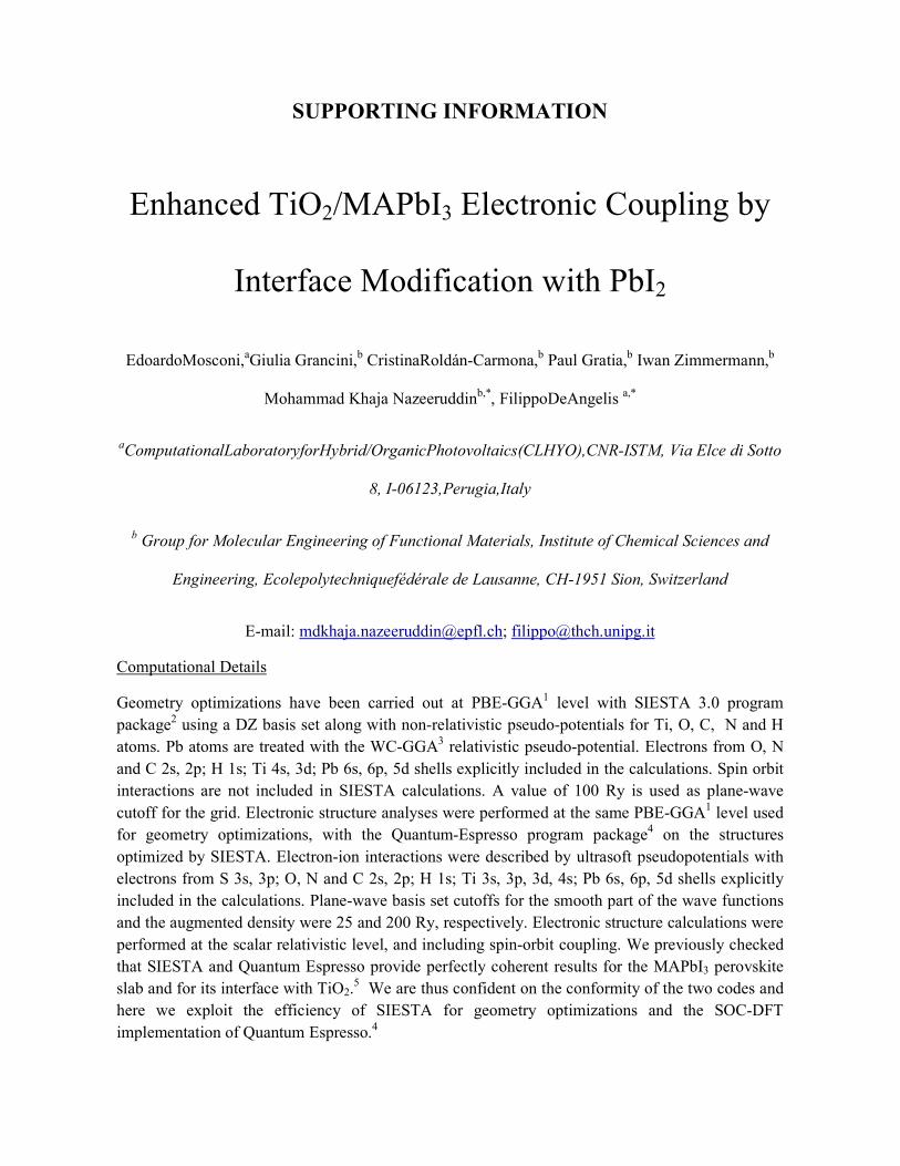
Figure S1.Partial Density of States (DOS) at SOC-GGA level of theory with summed contributions
from TiO2 (dashed) and perovskite (solid) contributions for the (110) TiO2/MAPbI3 MAI-
terminated (red) and PbI2-terminated (blue) interfaces. The DOS are calculated by introducing a
smearing (0.01 eV) of the orbital occupancies. Notice the tail extending below the conduction band
(at ca. 1 eV) in the PbI2-terminated system indicating stronger admixture of MAPbI3/TiO2 states.
Experimental details
Materials:Chemicals were purchased from Sigma-Aldrich and TCI Europe and used as received
without further purification. CH3NH3I was prepared similar to a previously published method7, in
brief: CH3NH3I, was synthesized by reacting 21.6 ml methylamine (40%wt in water, Aldrich) and
30 ml hydroiodic acid (57 wt% in water,Aldrich) in a 250 ml round-bottomed flask at 0 ºC for 2 h
with stirring. The white precipitate was recovered by evaporation at 50 ºC for 1 h. The product,
methylammonium iodide (CH3NH3I), was dissolved in ethanol, filtered and recrystallized from
diethyl ether, and dried at 60 ºC in a vacuum oven for 24 h.
Sample preparation: Thin films were fabricated following a one-step anti-solvent approach as
described elsewhere.6 The film were prepared on fluorine-doped tin oxide coated glass (NSG10)
substrates. After cleaning the substrates by ultrasonic and UV-ozone treatment, a 30 nm thick TiO2
blocking layer was deposited by spray pyrolysis following a procedure previously reported in the
literature.6 The mesoporous TiO2 layer was spin coated from a solution containing 150mg 30NRD
Dyesol paste per 1 ml of EtOH, at 5000rpm, 2000rpm/s, 10s, and annealed at 500°C for 15min. 1.25
M PbI2 /MAI (1:1) in DMSO was spin coated using chlorobenzene as an antisolvent. Different
compositions with 0 – 10– 20 % molar excess of PbI2 were also tested by fixing the MAI
concentration in the precursor solution and adjusting the amount of PbI2.The perovskite layer was
deposited inside a Nitrogen glovebox (MBraun) and annealed at 100 ºC during 45 min. A similar
approach was followed for the preparation of the PbI2 pre-treated sample where, prior to the
perovskite deposition, a thin film of PbI2 was deposited from 1.2 M solution in DMSO at 4000 rpm
and annealed at 100ºC during 10 minutes.After the annealing process, the perovskite films were
encapsulated inside inert N2atmosphere with a glass cover-slide to prevent any oxygen or air-
moisture induced degradation.
Solar cells
The solar cells were fabricated on FTO covered glass substrates based on a previously reported
architecture, where the active layer is sandwiched between a mesoporous TiO2 electron transport
material and 2,2′7,7′-tetrakis(N,N-di-p-methoxyphenylamine)-9,9′-spirobifluorene) (spiro-
OMeTAD) hole transport layer. After cleaning the substrates by ultrasonic and UV-ozone
treatment, a thin TiO2 compact layer of 25 nm was deposited on FTO via spray pyrolysis at 450°C,
followed by a sintering process of the layer at 450 oC during 30 minutes. Then a mesoporous TiO2
layer was deposited by spin coating a 30 nm particle paste (Dyesol 30 NR-D) diluted in ethanol for
10 s at 4000 rpm, to achieve 150 nm thick layer. These layers were sintered again at 450°C for 30
min under dry air flow. The perovskite films were prepared from a precursor solution 1.25 M of
both components PbI2 and CH3NH3I in dimethyl sulfoxide (DMSO) in the case of 1:1 molar ratio.
Different compositions with 10 – 20 % molar excess of PbI2 were also tested by fixing the MAI
concentration in the precursor solution and adjusting the amount of PbI2. The perovskite solution
was then deposited by a previously reported method in Ref [20]. This process consist of the
deposition of the precursor solution followed by chlorobenzene drop-casting in a similar way as the
solvent engineering method previously reported [20]. The resulted film was uncoloured and
transparent, indicating the formation of a smooth film of the CH3NH3I–PbI2–DMSO intermediate
phase. This film was then annealed at 100 C during 45 minutes in an inert atmosphere to favour a
good crystallization of the perovskite layer. The pre-treated sample was prepared following a
similar procedure but depositing a thin layer of PbI2 (1M in DMSO, 4000 rpm) and annealing it
during 10 minutes at 100ºC prior to the deposition of the perovskite solution. Finally, a 200 nm
layer of doped spiro-OMeTAD was deposited as the hole transport material prior to the deposition
of 100 nm gold as the electrode.
Micro-Raman Experiments
The micro Raman system is based on an optical microscope (Renishaw microscope, equipped with
5x, 20x, 50x and 100x short and long working distance microscope objectives) used to focus the
excitation light and collect it in a back scattering configuration, a monochromator, notch filters
system and a charge coupled detector. The sample is mounted on a translation stage of a Leica
microscope. The excitation used consists of a diode laser at 532 nm. The system has been calibrated
against the 520.5 cm-1 line of an internal silicon wafer. The spectra have been registered in the 60-
300 cm-1 range, particularly sensitive the Pb-I modes. The final data have been averaged over 30
accumulations in order to maximize the signal to noise ratio. The measurements were conducted at
room temperature on encapsulated sample. To prevent sample degradation or thermal effects the
laser power intensity is kept below 100µW.
Photoluminescence Experiments
The time-resolved PL experiments were performed with a spectrophotometer (Gilden Photonics)
using a pulsed source at 460 nm (Ps diode lasers BDS-SM, pulse with < 100 ps, from Photonic
Solutions, approx. 1mW power, 20MHz repetition rate, approx. 500 um spot radius) and the signal
was recorded at 770 nm by the Time Correlated Single Photon Counting detection technique with a
time resolution of 1 ns. The samples were excited from the perovskite side or from mesoporous
TiO2 side under ambient conditions. A monoexponential and bi-exponential fitting were used to
analyze the background-corrected PL decay signal.
XRD analysis
The X-ray diffractogram of the thin film was recorded on an X’Pert MPD PRO (PANalytical)
equipped with a ceramic tube providing Ni-filtered (CuKα = 1.54060 Å) radiation and a RTMS
X’Celerator (PANalytical). The data were collected at room temperature in the 2θ range 8 – 60 º. A
baseline correction was applied to compensate for the broad feature arising from the FTO glass and
anatase substrate.
SEM
Scanning electron microscope images have been taken by using a standard Zeiss Merlin microscope
at the CIME center at EPFL. The working distance was 2.9 mm and the voltage 2kV.
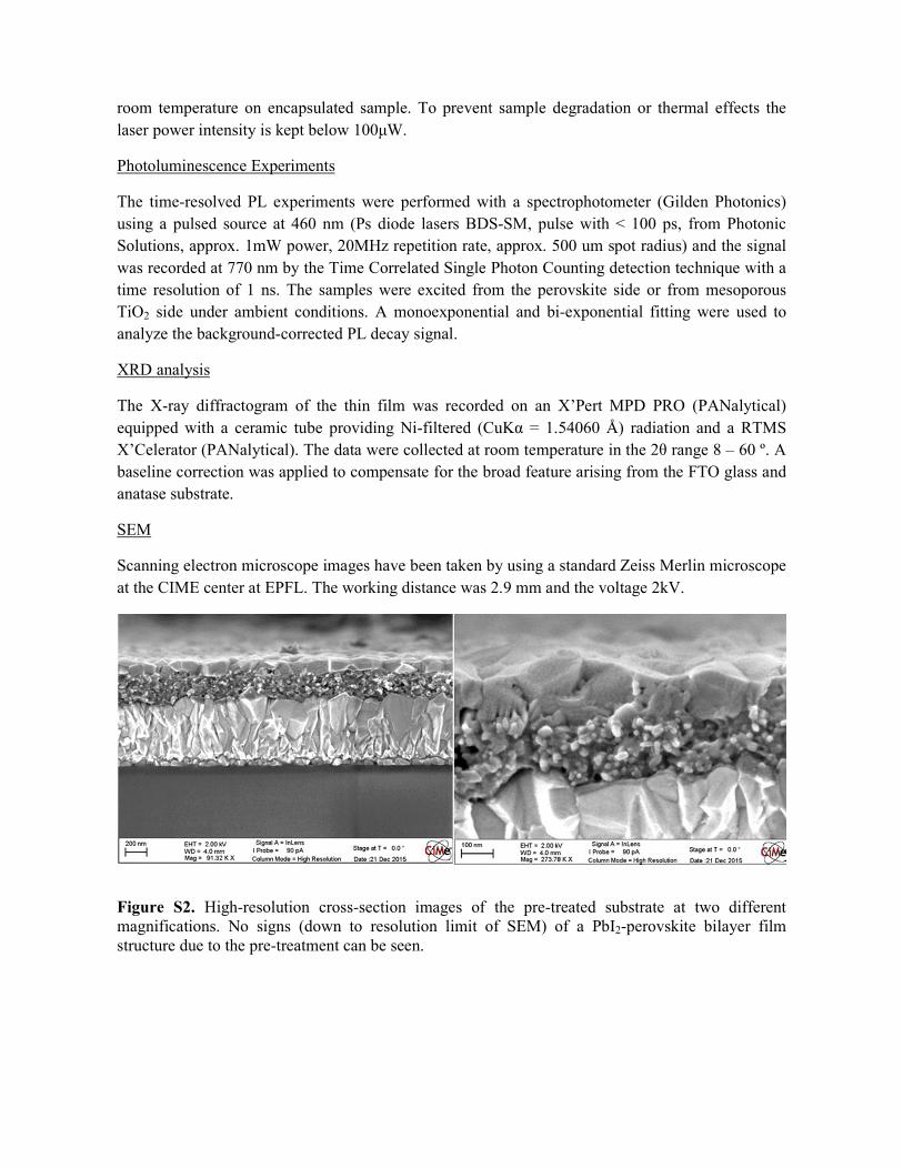
Figure S2. High-resolution cross-section images of the pre-treated substrate at two different magnifications. No signs (down to resolution limit of SEM) of a PbI2-perovskite bilayer film structure due to the pre-treatment can be seen.
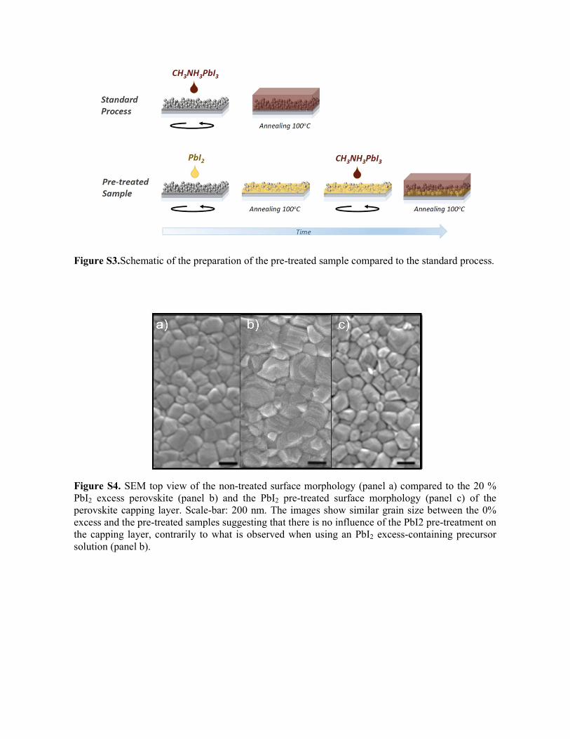
Figure S3.Schematic of the preparation of the pre-treated sample compared to the standard process.
Figure S4. SEM top view of the non-treated surface morphology (panel a) compared to the 20 % PbI2 excess perovskite (panel b) and the PbI2 pre-treated surface morphology (panel c) of the perovskite capping layer. Scale-bar: 200 nm. The images show similar grain size between the 0% excess and the pre-treated samples suggesting that there is no influence of the PbI2 pre-treatment on the capping layer, contrarily to what is observed when using an PbI2 excess-containing precursor solution (panel b).
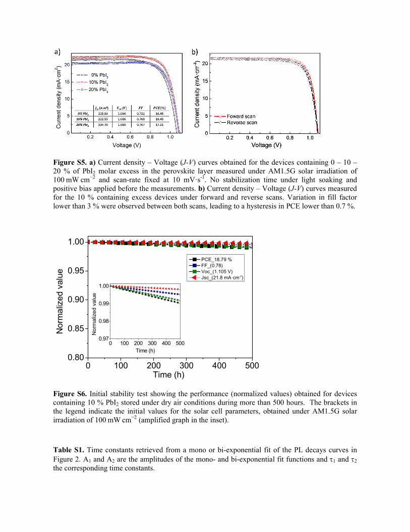
Figure S5. a) Current density – Voltage (J-V) curves obtained for the devices containing 0 – 10 – 20 % of PbI2 molar excess in the perovskite layer measured under AM1.5G solar irradiation of 100 mW cm−2 and scan-rate fixed at 10 mV·s-1. No stabilization time under light soaking and positive bias applied before the measurements. b) Current density – Voltage (J-V) curves measured for the 10 % containing excess devices under forward and reverse scans. Variation in fill factor lower than 3 % were observed between both scans, leading to a hysteresis in PCE lower than 0.7 %.
Figure S6. Initial stability test showing the performance (normalized values) obtained for devices containing 10 % PbI2 stored under dry air conditions during more than 500 hours. The brackets in the legend indicate the initial values for the solar cell parameters, obtained under AM1.5G solar irradiation of 100 mW cm−2 (amplified graph in the inset).
Table S1. Time constants retrieved from a mono or bi-exponential fit of the PL decays curves in Figure 2. A1 and A2 are the amplitudes of the mono- and bi-exponential fit functions and τ1 and τ2 the corresponding time constants.
0 100 200 300 400 5000.80
0.85
0.90
0.95
1.00
Norm
aliz
ed v
alu
e
PCE_18.79 %
FF_(0.78)
Voc_(1.105 V)
Jsc_(21.8 mA�cm-2)
Time (h)
0 100 200 300 400 5000.97
0.98
0.99
1.00
No
rma
lize
d v
alu
e
Time (h)
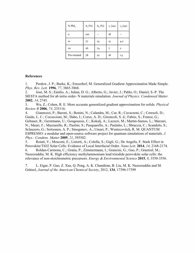
% PbI2 A1 (%) A2 (%) τ1 (ns) τ2 (ns)
0 100 -- 18 --
10 77 23 13 4.2
20 26 74 7 2
Pre-treated 78 22 18 1.5
References
1. Perdew, J. P.; Burke, K.; Ernzerhof, M. Generalized Gradient Approximation Made Simple. Phys. Rev. Lett. 1996, 77, 3865-3868. 2. José, M. S.; Emilio, A.; Julian, D. G.; Alberto, G.; Javier, J.; Pablo, O.; Daniel, S.-P. The SIESTA method for ab initio order- N materials simulation. Journal of Physics: Condensed Matter
2002, 14, 2745. 3. Wu, Z.; Cohen, R. E. More accurate generalized gradient approximation for solids. Physical
Review B 2006, 73, 235116. 4. Giannozzi, P.; Baroni, S.; Bonini, N.; Calandra, M.; Car, R.; Cavazzoni, C.; Ceresoli, D.; Guido, L. C.; Cococcioni, M.; Dabo, I.; Corso, A. D.; Gironcoli, S. d.; Fabris, S.; Fratesi, G.; Gebauer, R.; Gerstmann, U.; Gougoussis, C.; Kokalj, A.; Lazzeri, M.; Martin-Samos, L.; Marzari, N.; Mauri, F.; Mazzarello, R.; Paolini, S.; Pasquarello, A.; Paulatto, L.; Sbraccia, C.; Scandolo, S.; Sclauzero, G.; Seitsonen, A. P.; Smogunov, A.; Umari, P.; Wentzcovitch, R. M. QUANTUM ESPRESSO: a modular and open-source software project for quantum simulations of materials. J. Phys.: Condens. Matter 2009, 21, 395502. 5. Roiati, V.; Mosconi, E.; Listorti, A.; Colella, S.; Gigli, G.; De Angelis, F. Stark Effect in Perovskite/TiO2 Solar Cells: Evidence of Local Interfacial Order. Nano Lett. 2014, 14, 2168-2174. 6. Roldan-Carmona, C.; Gratia, P.; Zimmermann, I.; Grancini, G.; Gao, P.; Graetzel, M.; Nazeeruddin, M. K. High efficiency methylammonium lead triiodide perovskite solar cells: the relevance of non-stoichiometric precursors. Energy & Environmental Science 2015, 8, 3550-3556.
7. L. Etgar, P. Gao, Z. Xue, Q. Peng, A. K. Chandiran, B. Liu, M. K. Nazeeruddin and M. Grätzel, Journal of the American Chemical Society, 2012, 134, 17396-17399