Embed Size (px)
Citation preview
IMEC Free Mini@sic Fabrication on TSMC 0.18 um Technology
A) Identification Title: Analog and RFID circuits Adviser Professor(s) Prof. PhD. Wilhelmus Van Noije Students involved (names and aimed degrees) PAULO ROBERTO DE CARVALHO-‐ Master Student LUCAS SEVERO COMPASSI – PhD. Student THIAGO OLIVEIRA WEBBER – PhD. BRUNO CAVALCANTE SANCHES – PhD. Student HUGO DANIEL HERNÁNDEZ HERRERA – PhD. JOSÉ ALEJANDRO AMAYA PALACIO – PhD. Student RODRIGO PEDROSO MENDES – Undergrad Student Institution (University/Faculty) University of Sao Paulo – Polytechnic School of Engineering Type of Circuit Design: ( ) Digital; (X) mixed signal; ( ) analog; ( ) RF Date of the circuit tape-‐out of the run: 20/03/2015 Date of receiving the chips at your institution: 17/08/2015 Date of the report and/or of later up-‐date: 17/02/2016
B) Short Description of the circuit: (function, proposed innovation, number of transistors, passive components, screen shot of the chip layout, etc)
The IC prototyped in Mini@sic 2015/1 program has four independent circuits: (a)
Numerically Controlled Oscillator (NCO), (b) Operational Transconductance Amplifier (OTA), (c) Voltage Reference (Vref) and, (d) a RFID tag. Following we present a short description about them. (a) The main circuit is the NCO used for Electrical Bio-‐Impedance Spectroscopy. The NCO is based on the iterative architecture of CORDIC processor (the iterative architecture implies efficient relation between area and speed) to generate digital value of sine and cosine in the frequency range of 100 Hz to 1 MHz. The NCO includes a novelty angle sequencer in order to modify the frequency value. The NCO basic structure includes an Angle generator module composed of a frequency selector, a phase accumulator, a pre-‐rotator module and a sine/cosine converter. To minimize the number of pins of the integrated circuit, we used a 5-‐bit frequency selector and an output function selector. The Angle generator is composed of a 5-‐bit frequency selector and a phase accumulator. The final layout of the circuit is shown in Fig. 1(a). The total area is 0.017 mm2 and used 533 standard cells from the “tcb018gbwp7t” library. The NCO circuit was routed using six metal layers. (b) The OTA and (c) Vref design were performed with two new methodologies for analog integrated circuit design that explores the design space solutions with an optimization algorithm. These designs were used to validate the developed methodologies in our research group (LSI) at USP. The OTA circuit is a high voltage gain selfbiased folded cascade amplifier composed by 14
transistors. The circuit was designed to satisfy the specifications of a high stability voltage controlled current source, used in an electrical impedance spectroscopy cervical cancer detector. The designed OTA layout, shown in Fig. 1(b), has a total area of 0.027 mm². The Vref circuit was designed with the specifications required by a charge sense amplifier of the SAMPA IC, used in the Large Ion Hadron Experiment (ALICE) of the CERN lab. The used circuit topology is resistant to low level radiations. The output reference voltage is equal to 600 mV and, the circuit occupy an area of 0.059 mm². Fig. 1(c) shows the circuit layout. (d) The RFID tag circuit was designed by an undergraduate student of USP and was part of his final graduation project (thesis). The circuits is composed by a RF to DC rectifier, a modulator, a demodulator, an oscillator, a voltage regulator and a power on reset (PoR) circuit. The circuit total area is 0.194 mm² and the layout is shown in Fig. 1(d).
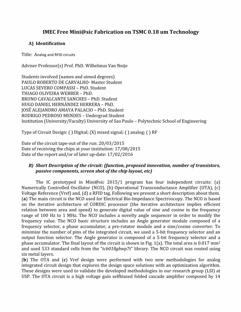
The final layout of the USP mini@sic chip and the die photography are shown in Fig. 2.
(a) (b) (c) (d) Fig. 1 Layout of the prototyped circuits: (a) NCO, (b) OTA, (c) Vref and (d) RFID Circuit.
(a) (b)
Fig. 2 USP Prototype mini@asic: (a) layout and (b) photography of the chip.
C) Main results and representative performance data or curves, picture of the IC, does
circuit function as expected, etc
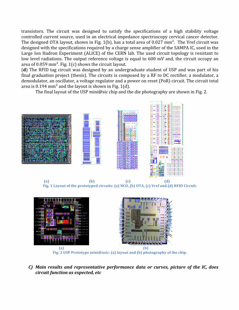
Ten samples of the mini@sic chip were bounded into a QFN48 package and mounted on a PCB, as shown in Fig. 3(a), for evaluation tests of the NCO, OTA and Vref circuits. For the RFID measurements, a specific PCB was designed and, the RF measurements were realized with microprobes directly connected to the die, as shown in Fig. 3(b).
(a) (b) Fig. 3 PCB Evaluation Board for MiniASIC tests: (a) NCO, OTA and Vref and (b) RFID block.
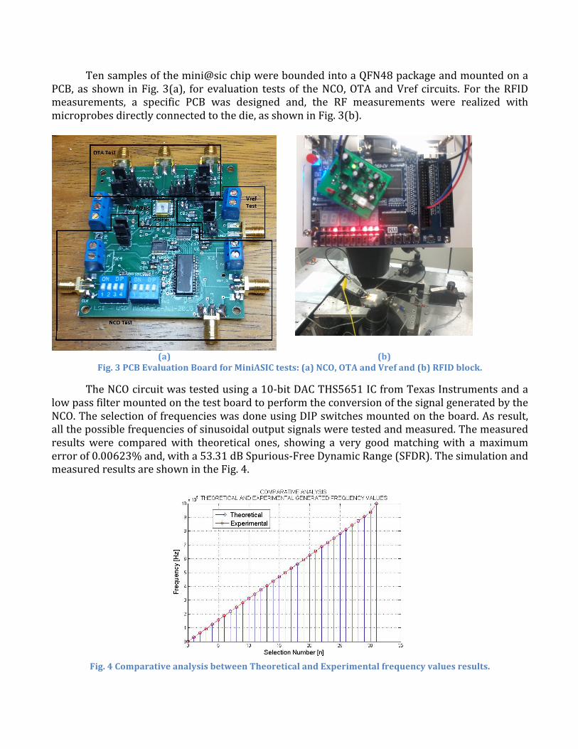
The NCO circuit was tested using a 10-‐bit DAC THS5651 IC from Texas Instruments and a low pass filter mounted on the test board to perform the conversion of the signal generated by the NCO. The selection of frequencies was done using DIP switches mounted on the board. As result, all the possible frequencies of sinusoidal output signals were tested and measured. The measured results were compared with theoretical ones, showing a very good matching with a maximum error of 0.00623% and, with a 53.31 dB Spurious-‐Free Dynamic Range (SFDR). The simulation and measured results are shown in the Fig. 4.
Fig. 4 Comparative analysis between Theoretical and Experimental frequency values results.
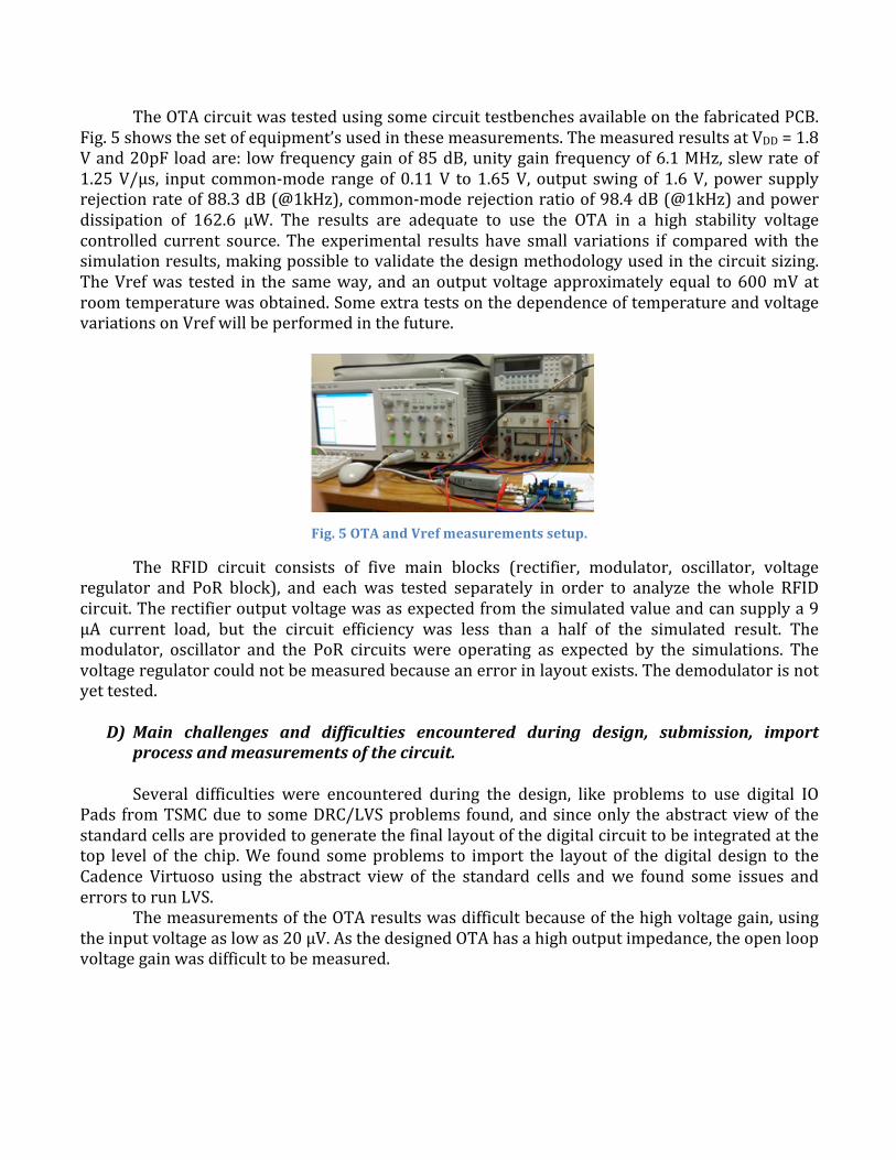
The OTA circuit was tested using some circuit testbenches available on the fabricated PCB. Fig. 5 shows the set of equipment’s used in these measurements. The measured results at VDD = 1.8 V and 20pF load are: low frequency gain of 85 dB, unity gain frequency of 6.1 MHz, slew rate of 1.25 V/µs, input common-‐mode range of 0.11 V to 1.65 V, output swing of 1.6 V, power supply rejection rate of 88.3 dB (@1kHz), common-‐mode rejection ratio of 98.4 dB (@1kHz) and power dissipation of 162.6 µW. The results are adequate to use the OTA in a high stability voltage controlled current source. The experimental results have small variations if compared with the simulation results, making possible to validate the design methodology used in the circuit sizing. The Vref was tested in the same way, and an output voltage approximately equal to 600 mV at room temperature was obtained. Some extra tests on the dependence of temperature and voltage variations on Vref will be performed in the future.
Fig. 5 OTA and Vref measurements setup.
The RFID circuit consists of five main blocks (rectifier, modulator, oscillator, voltage regulator and PoR block), and each was tested separately in order to analyze the whole RFID circuit. The rectifier output voltage was as expected from the simulated value and can supply a 9 µA current load, but the circuit efficiency was less than a half of the simulated result. The modulator, oscillator and the PoR circuits were operating as expected by the simulations. The voltage regulator could not be measured because an error in layout exists. The demodulator is not yet tested.
D) Main challenges and difficulties encountered during design, submission, import
process and measurements of the circuit.
Several difficulties were encountered during the design, like problems to use digital IO Pads from TSMC due to some DRC/LVS problems found, and since only the abstract view of the standard cells are provided to generate the final layout of the digital circuit to be integrated at the top level of the chip. We found some problems to import the layout of the digital design to the Cadence Virtuoso using the abstract view of the standard cells and we found some issues and errors to run LVS.
The measurements of the OTA results was difficult because of the high voltage gain, using the input voltage as low as 20 µV. As the designed OTA has a high output impedance, the open loop voltage gain was difficult to be measured.

E) Resulting publications (submitted, accepted or published) and degrees earned by students
The NCO results is part of a Master and a PhD works. The NCO results was submitted to 2016
IEEE Frequency Control Symposium – IFCS 2016, New Orleans, USA, May 9 -‐ 12 (http://ifcs2016.org/), and was accepted and selected as finalist of a Student Paper Competition:
• Title: Area optimized CORDIC-‐based Numerically Controlled Oscillator for Electrical Bio-‐impedance Spectroscopy
The OTA and Vref results were used to validate the design methodologies and the results are part of two PhD works (one of them was concluded). The RFID circuit results were part of a final graduation project (Undergraduate conclusion thesis) in 2015, with the title: Projeto de um sensor de temperatura RFID integrado em tecnologia CMOS (RFID temperature sensor design integrated in CMOS technology).