Embed Size (px)
Citation preview
Altera Corporation 2–1May 2007
2. Stratix II Architecture
Functional Description
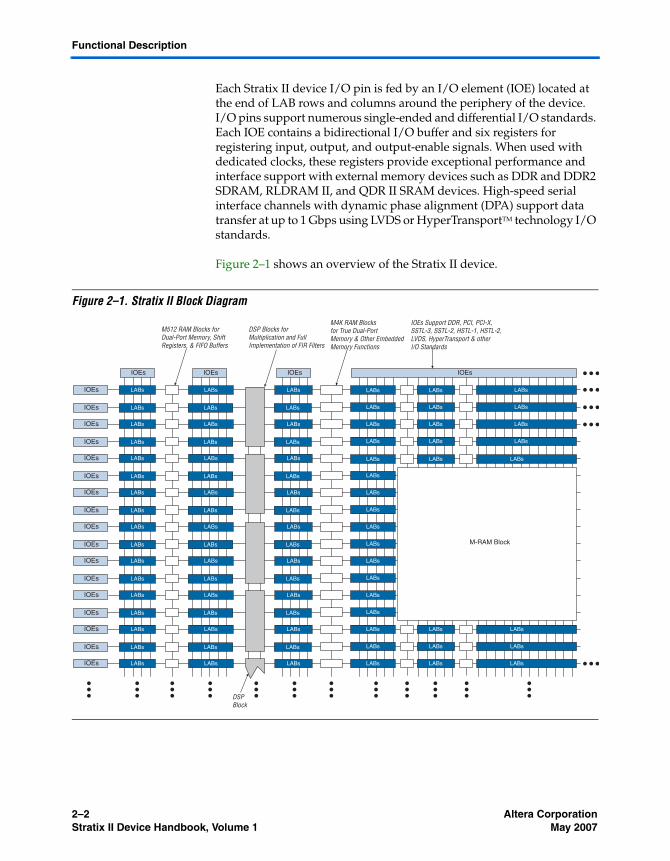
Stratix® II devices contain a two-dimensional row- and column-based architecture to implement custom logic. A series of column and row interconnects of varying length and speed provides signal interconnects between logic array blocks (LABs), memory block structures (M512 RAM, M4K RAM, and M-RAM blocks), and digital signal processing (DSP) blocks.
Each LAB consists of eight adaptive logic modules (ALMs). An ALM is the Stratix II device family’s basic building block of logic providing efficient implementation of user logic functions. LABs are grouped into rows and columns across the device.
M512 RAM blocks are simple dual-port memory blocks with 512 bits plus parity (576 bits). These blocks provide dedicated simple dual-port or single-port memory up to 18-bits wide at up to 500 MHz. M512 blocks are grouped into columns across the device in between certain LABs.
M4K RAM blocks are true dual-port memory blocks with 4K bits plus parity (4,608 bits). These blocks provide dedicated true dual-port, simple dual-port, or single-port memory up to 36-bits wide at up to 550 MHz. These blocks are grouped into columns across the device in between certain LABs.
M-RAM blocks are true dual-port memory blocks with 512K bits plus parity (589,824 bits). These blocks provide dedicated true dual-port, simple dual-port, or single-port memory up to 144-bits wide at up to 420 MHz. Several M-RAM blocks are located individually in the device's logic array.
DSP blocks can implement up to either eight full-precision 9 × 9-bit multipliers, four full-precision 18 × 18-bit multipliers, or one full-precision 36 × 36-bit multiplier with add or subtract features. The DSP blocks support Q1.15 format rounding and saturation in the multiplier and accumulator stages. These blocks also contain shift registers for digital signal processing applications, including finite impulse response (FIR) and infinite impulse response (IIR) filters. DSP blocks are grouped into columns across the device and operate at up to 450 MHz.
SII51002-4.3
2–2 Altera CorporationStratix II Device Handbook, Volume 1 May 2007
Functional Description
Each Stratix II device I/O pin is fed by an I/O element (IOE) located at the end of LAB rows and columns around the periphery of the device. I/O pins support numerous single-ended and differential I/O standards. Each IOE contains a bidirectional I/O buffer and six registers for registering input, output, and output-enable signals. When used with dedicated clocks, these registers provide exceptional performance and interface support with external memory devices such as DDR and DDR2 SDRAM, RLDRAM II, and QDR II SRAM devices. High-speed serial interface channels with dynamic phase alignment (DPA) support data transfer at up to 1 Gbps using LVDS or HyperTransportTM technology I/O standards.
Figure 2–1 shows an overview of the Stratix II device.
Figure 2–1. Stratix II Block Diagram
M512 RAM Blocks for Dual-Port Memory, Shift Registers, & FIFO Buffers
DSP Blocks forMultiplication and FullImplementation of FIR Filters
M4K RAM Blocksfor True Dual-Port Memory & Other EmbeddedMemory Functions
IOEs Support DDR, PCI, PCI-X, SSTL-3, SSTL-2, HSTL-1, HSTL-2, LVDS, HyperTransport & otherI/O Standards
IOEs
IOEs
IOEs
IOEs
IOEs
IOEs
IOEs
IOEs
IOEs
IOEs
IOEs
IOEs
IOEs
IOEs
IOEs
IOEs
IOEs
LABs
LABs
IOEs
LABs
LABs
LABs
LABs
LABs
LABs
LABs
LABs
LABs
LABs
LABs
LABs
LABs
LABs
LABs
LABs
LABs
IOEs
LABs
LABs
LABs
LABs
LABs
LABs
LABs
LABs
LABs
LABs
LABs
LABs
LABs
LABs
LABs
LABs LABs
LABs
IOEs IOEs
LABs
LABs LABs
LABs LABs
LABs
LABs
LABs
LABs
LABs
LABs
LABs
LABs
LABs
LABs
LABs
LABs
LABs
LABs
LABs LABs
LABs
LABs
LABs
LABs
LABs
LABs
LABs
LABs
LABs
LABs
LABs
LABsLABs
LABsLABs
LABsLABs
LABs
LABs
LABs
LABs
LABs
LABs
LABs
LABs
LABs
DSPBlock
M-RAM Block
Altera Corporation 2–3May 2007 Stratix II Device Handbook, Volume 1
Stratix II Architecture
The number of M512 RAM, M4K RAM, and DSP blocks varies by device along with row and column numbers and M-RAM blocks. Table 2–1 lists the resources available in Stratix II devices.
Logic Array Blocks
Each LAB consists of eight ALMs, carry chains, shared arithmetic chains, LAB control signals, local interconnect, and register chain connection lines. The local interconnect transfers signals between ALMs in the same LAB. Register chain connections transfer the output of an ALM register to the adjacent ALM register in an LAB. The Quartus® II Compiler places associated logic in an LAB or adjacent LABs, allowing the use of local, shared arithmetic chain, and register chain connections for performance and area efficiency. Figure 2–2 shows the Stratix II LAB structure.
Table 2–1. Stratix II Device Resources
Device M512 RAM Columns/Blocks
M4K RAM Columns/Blocks
M-RAM Blocks
DSP Block Columns/Blocks
LAB Columns LAB Rows
EP2S15 4 / 104 3 / 78 0 2 / 12 30 26
EP2S30 6 / 202 4 / 144 1 2 / 16 49 36
EP2S60 7 / 329 5 / 255 2 3 / 36 62 51
EP2S90 8 / 488 6 / 408 4 3 / 48 71 68
EP2S130 9 / 699 7 / 609 6 3 / 63 81 87
EP2S180 11 / 930 8 / 768 9 4 / 96 100 96
2–4 Altera CorporationStratix II Device Handbook, Volume 1 May 2007
Logic Array Blocks
Figure 2–2. Stratix II LAB Structure
LAB Interconnects
The LAB local interconnect can drive ALMs in the same LAB. It is driven by column and row interconnects and ALM outputs in the same LAB. Neighboring LABs, M512 RAM blocks, M4K RAM blocks, M-RAM blocks, or DSP blocks from the left and right can also drive an LAB's local interconnect through the direct link connection. The direct link connection feature minimizes the use of row and column interconnects, providing higher performance and flexibility. Each ALM can drive 24 ALMs through fast local and direct link interconnects. Figure 2–3 shows the direct link connection.
Direct linkinterconnect fromadjacent block
Direct linkinterconnect toadjacent block
Row Interconnects ofVariable Speed & Length
Column Interconnects ofVariable Speed & Length
Local Interconnect is Driven from Either Side by Columns & LABs,
& from Above by Rows
Local Interconnect LAB
Direct linkinterconnect from adjacent block
Direct linkinterconnect toadjacent block
ALMs
Altera Corporation 2–5May 2007 Stratix II Device Handbook, Volume 1
Stratix II Architecture
Figure 2–3. Direct Link Connection
LAB Control Signals
Each LAB contains dedicated logic for driving control signals to its ALMs. The control signals include three clocks, three clock enables, two asynchronous clears, synchronous clear, asynchronous preset/load, and synchronous load control signals. This gives a maximum of 11 control signals at a time. Although synchronous load and clear signals are generally used when implementing counters, they can also be used with other functions.
Each LAB can use three clocks and three clock enable signals. However, there can only be up to two unique clocks per LAB, as shown in the LAB control signal generation circuit in Figure 2–4. Each LAB's clock and clock enable signals are linked. For example, any ALM in a particular LAB using the labclk1 signal also uses labclkena1. If the LAB uses both the rising and falling edges of a clock, it also uses two LAB-wide clock signals. De-asserting the clock enable signal turns off the corresponding LAB-wide clock.
Each LAB can use two asynchronous clear signals and an asynchronous load/preset signal. By default, the Quartus II software uses a NOT gate push-back technique to achieve preset. If you disable the NOT gate push-up option or assign a given register to power up high using the Quartus II software, the preset is achieved using the asynchronous load
ALMs
Direct linkinterconnectto right
Direct link interconnect fromright LAB, TriMatrix memoryblock, DSP block, or IOE output
Direct link interconnect fromleft LAB, TriMatrix memory
block, DSP block, or IOE output
LocalInterconnect
Direct linkinterconnect
to left
2–6 Altera CorporationStratix II Device Handbook, Volume 1 May 2007
Adaptive Logic Modules
signal with asynchronous load data input tied high. When the asynchronous load/preset signal is used, the labclkena0 signal is no longer available.
The LAB row clocks [5..0] and LAB local interconnect generate the LAB-wide control signals. The MultiTrackTM interconnect's inherent low skew allows clock and control signal distribution in addition to data. Figure 2–4 shows the LAB control signal generation circuit.
Figure 2–4. LAB-Wide Control Signals
Adaptive Logic Modules
The basic building block of logic in the Stratix II architecture, the adaptive logic module (ALM), provides advanced features with efficient logic utilization. Each ALM contains a variety of look-up table (LUT)-based resources that can be divided between two adaptive LUTs (ALUTs). With up to eight inputs to the two ALUTs, one ALM can implement various combinations of two functions. This adaptability allows the ALM to be
Dedicated Row LAB Clocks
Local Interconnect
Local Interconnect
Local Interconnect
Local Interconnect
Local Interconnect
Local Interconnect
labclk2 syncload
labclkena0or asyncloador labpreset
labclk0 labclk1 labclr1
labclkena1 labclkena2 labclr0 synclr
6
6
6
There are two uniqueclock signals per LAB.
Altera Corporation 2–7May 2007 Stratix II Device Handbook, Volume 1
Stratix II Architecture
completely backward-compatible with four-input LUT architectures. One ALM can also implement any function of up to six inputs and certain seven-input functions.
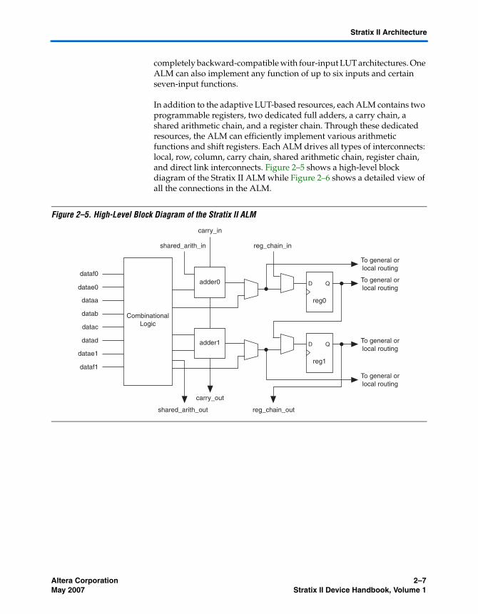
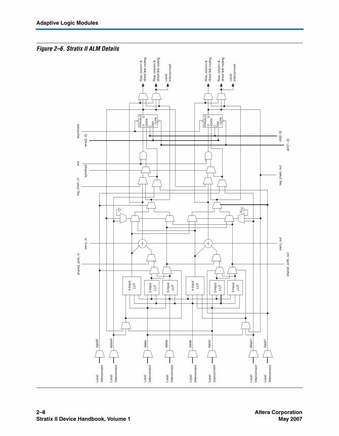
In addition to the adaptive LUT-based resources, each ALM contains two programmable registers, two dedicated full adders, a carry chain, a shared arithmetic chain, and a register chain. Through these dedicated resources, the ALM can efficiently implement various arithmetic functions and shift registers. Each ALM drives all types of interconnects: local, row, column, carry chain, shared arithmetic chain, register chain, and direct link interconnects. Figure 2–5 shows a high-level block diagram of the Stratix II ALM while Figure 2–6 shows a detailed view of all the connections in the ALM.
Figure 2–5. High-Level Block Diagram of the Stratix II ALM
D QTo general orlocal routing
reg0
To general orlocal routing
datae0
dataf0
shared_arith_in
shared_arith_out
reg_chain_in
reg_chain_out
adder0
dataa
datab
datac
datad
CombinationalLogic
datae1
dataf1
D QTo general orlocal routing
reg1
To general orlocal routing
adder1
carry_in
carry_out
2–8 Altera CorporationStratix II Device Handbook, Volume 1 May 2007
Adaptive Logic Modules
Figure 2–6. Stratix II ALM Details
PR
N/A
LD
CLR
N
D AD
ATA
EN
A
Q
PR
N/A
LD
CLR
N
D AD
ATA
EN
A
Q
4-In
put
LUT
3-In
put
LUT
3-In
put
LUT
4-In
put
LUT
3-In
put
LUT
3-In
put
LUT
data
a
data
c
data
e0
data
f0
data
f1
data
e1
data
b
data
d
VC
C
reg_
chai
n_in
sclr
asyn
cloa
d
sync
load
ena[
2..0
]
shar
ed_a
rith_
in
carr
y_in
carr
y_ou
tcl
k[2.
.0]
Loca
lIn
terc
onne
ct
Row
, col
umn
&di
rect
link
rou
ting
Row
, col
umn
&di
rect
link
rou
ting
Loca
lIn
terc
onne
ct
Row
, col
umn
&di
rect
link
rou
ting
Row
, col
umn
&di
rect
link
rou
ting
reg_
chai
n_ou
t
shar
ed_a
rith_
out
aclr[
1..0
]
Loca
l
Inte
rcon
nect
Loca
l
Inte
rcon
nect
Loca
l
Inte
rcon
nect
Loca
l
Inte
rcon
nect
Loca
l
Inte
rcon
nect
Loca
l
Inte
rcon
nect
Loca
l
Inte
rcon
nect
Loca
l
Inte
rcon
nect
Altera Corporation 2–9May 2007 Stratix II Device Handbook, Volume 1
Stratix II Architecture
One ALM contains two programmable registers. Each register has data, clock, clock enable, synchronous and asynchronous clear, asynchronous load data, and synchronous and asynchronous load/preset inputs. Global signals, general-purpose I/O pins, or any internal logic can drive the register's clock and clear control signals. Either general-purpose I/O pins or internal logic can drive the clock enable, preset, asynchronous load, and asynchronous load data. The asynchronous load data input comes from the datae or dataf input of the ALM, which are the same inputs that can be used for register packing. For combinational functions, the register is bypassed and the output of the LUT drives directly to the outputs of the ALM.
Each ALM has two sets of outputs that drive the local, row, and column routing resources. The LUT, adder, or register output can drive these output drivers independently (see Figure 2–6). For each set of output drivers, two ALM outputs can drive column, row, or direct link routing connections, and one of these ALM outputs can also drive local interconnect resources. This allows the LUT or adder to drive one output while the register drives another output. This feature, called register packing, improves device utilization because the device can use the register and the combinational logic for unrelated functions. Another special packing mode allows the register output to feed back into the LUT of the same ALM so that the register is packed with its own fan-out LUT. This provides another mechanism for improved fitting. The ALM can also drive out registered and unregistered versions of the LUT or adder output.
f See the Performance & Logic Efficiency Analysis of Stratix II Devices White Paper for more information on the efficiencies of the Stratix II ALM and comparisons with previous architectures.
ALM Operating Modes
The Stratix II ALM can operate in one of the following modes:
■ Normal mode■ Extended LUT mode■ Arithmetic mode■ Shared arithmetic mode
Each mode uses ALM resources differently. In each mode, eleven available inputs to the ALM--the eight data inputs from the LAB local interconnect; carry-in from the previous ALM or LAB; the shared arithmetic chain connection from the previous ALM or LAB; and the register chain connection--are directed to different destinations to implement the desired logic function. LAB-wide signals provide clock, asynchronous clear, asynchronous preset/load, synchronous clear,
2–10 Altera CorporationStratix II Device Handbook, Volume 1 May 2007
Adaptive Logic Modules
synchronous load, and clock enable control for the register. These LAB-wide signals are available in all ALM modes. See the “LAB Control Signals” section for more information on the LAB-wide control signals.
The Quartus II software and supported third-party synthesis tools, in conjunction with parameterized functions such as library of parameterized modules (LPM) functions, automatically choose the appropriate mode for common functions such as counters, adders, subtractors, and arithmetic functions. If required, you can also create special-purpose functions that specify which ALM operating mode to use for optimal performance.
Normal Mode
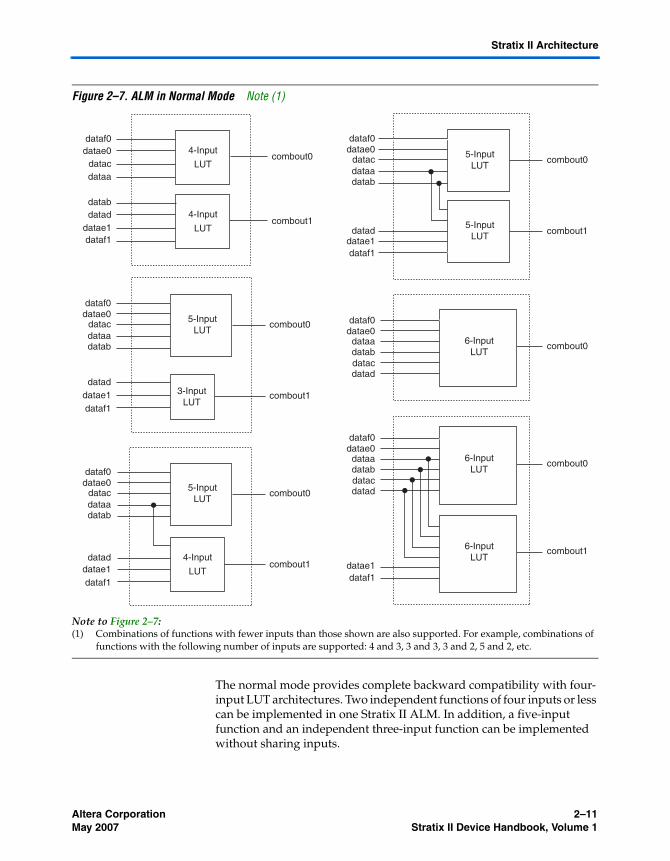
The normal mode is suitable for general logic applications and combinational functions. In this mode, up to eight data inputs from the LAB local interconnect are inputs to the combinational logic. The normal mode allows two functions to be implemented in one Stratix II ALM, or an ALM to implement a single function of up to six inputs. The ALM can support certain combinations of completely independent functions and various combinations of functions which have common inputs. Figure 2–7 shows the supported LUT combinations in normal mode.
Altera Corporation 2–11May 2007 Stratix II Device Handbook, Volume 1
Stratix II Architecture
Figure 2–7. ALM in Normal Mode Note (1)
Note to Figure 2–7:(1) Combinations of functions with fewer inputs than those shown are also supported. For example, combinations of
functions with the following number of inputs are supported: 4 and 3, 3 and 3, 3 and 2, 5 and 2, etc.
The normal mode provides complete backward compatibility with four-input LUT architectures. Two independent functions of four inputs or less can be implemented in one Stratix II ALM. In addition, a five-input function and an independent three-input function can be implemented without sharing inputs.
6-InputLUT
dataf0datae0
dataf0datae0
dataadatab
dataadatab
datab
datac
datac
dataf0datae0
dataadatac
6-InputLUT
datad
datad
datae1
combout0
combout1
combout0
combout1
combout0
combout1
dataf1
datae1dataf1
dataddatae1dataf1
4-Input
LUT
4-Input
LUT
4-Input
LUT
6-InputLUT
dataf0datae0dataadatabdatacdatad
combout0
5-InputLUT
5-InputLUT
dataf0datae0
dataadatab
datac
datad
combout0
combout1datae1dataf1
5-InputLUT
dataf0datae0
dataadatab
datac
datad
combout0
combout1datae1dataf1
5-InputLUT
3-InputLUT
2–12 Altera CorporationStratix II Device Handbook, Volume 1 May 2007
Adaptive Logic Modules
For the packing of two five-input functions into one ALM, the functions must have at least two common inputs. The common inputs are dataa and datab. The combination of a four-input function with a five-input function requires one common input (either dataa or datab).
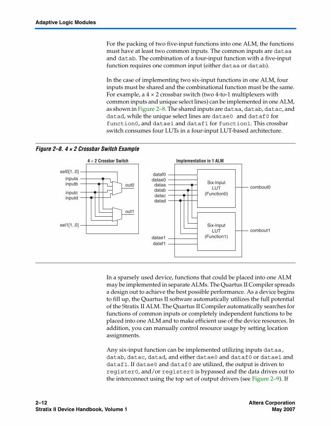
In the case of implementing two six-input functions in one ALM, four inputs must be shared and the combinational function must be the same. For example, a 4 × 2 crossbar switch (two 4-to-1 multiplexers with common inputs and unique select lines) can be implemented in one ALM, as shown in Figure 2–8. The shared inputs are dataa, datab, datac, and datad, while the unique select lines are datae0 and dataf0 for function0, and datae1 and dataf1 for function1. This crossbar switch consumes four LUTs in a four-input LUT-based architecture.
Figure 2–8. 4 × 2 Crossbar Switch Example
In a sparsely used device, functions that could be placed into one ALM may be implemented in separate ALMs. The Quartus II Compiler spreads a design out to achieve the best possible performance. As a device begins to fill up, the Quartus II software automatically utilizes the full potential of the Stratix II ALM. The Quartus II Compiler automatically searches for functions of common inputs or completely independent functions to be placed into one ALM and to make efficient use of the device resources. In addition, you can manually control resource usage by setting location assignments.
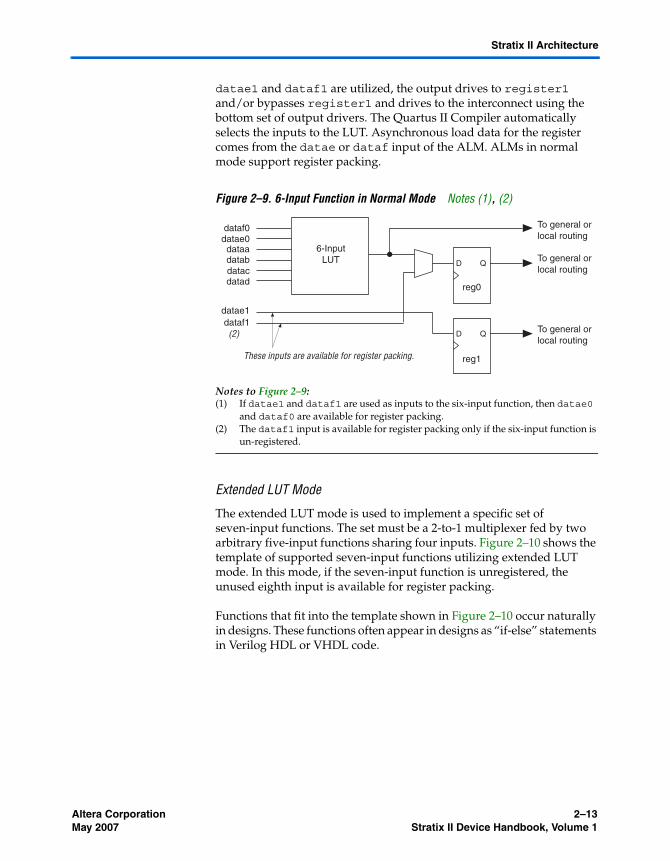
Any six-input function can be implemented utilizing inputs dataa, datab, datac, datad, and either datae0 and dataf0 or datae1 and dataf1. If datae0 and dataf0 are utilized, the output is driven to register0, and/or register0 is bypassed and the data drives out to the interconnect using the top set of output drivers (see Figure 2–9). If
Six-InputLUT
(Function0)
dataf0datae0
dataadatabdatac
Six-InputLUT
(Function1)
datad
datae1
combout0
combout1
dataf1
inputa
sel0[1..0]
sel1[1..0]
inputb
inputcinputd
out0
out1
4 × 2 Crossbar Switch Implementation in 1 ALM
Altera Corporation 2–13May 2007 Stratix II Device Handbook, Volume 1
Stratix II Architecture
datae1 and dataf1 are utilized, the output drives to register1 and/or bypasses register1 and drives to the interconnect using the bottom set of output drivers. The Quartus II Compiler automatically selects the inputs to the LUT. Asynchronous load data for the register comes from the datae or dataf input of the ALM. ALMs in normal mode support register packing.
Figure 2–9. 6-Input Function in Normal Mode Notes (1), (2)
Notes to Figure 2–9:(1) If datae1 and dataf1 are used as inputs to the six-input function, then datae0
and dataf0 are available for register packing.(2) The dataf1 input is available for register packing only if the six-input function is
un-registered.
Extended LUT Mode
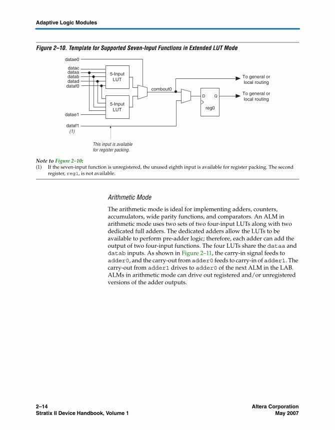
The extended LUT mode is used to implement a specific set of seven-input functions. The set must be a 2-to-1 multiplexer fed by two arbitrary five-input functions sharing four inputs. Figure 2–10 shows the template of supported seven-input functions utilizing extended LUT mode. In this mode, if the seven-input function is unregistered, the unused eighth input is available for register packing.
Functions that fit into the template shown in Figure 2–10 occur naturally in designs. These functions often appear in designs as “if-else” statements in Verilog HDL or VHDL code.
6-InputLUT
dataf0datae0
dataadatabdatacdatad
datae1dataf1
D Q
D Q
To general orlocal routing
To general orlocal routing
To general orlocal routing
reg0
reg1These inputs are available for register packing.
(2)
2–14 Altera CorporationStratix II Device Handbook, Volume 1 May 2007
Adaptive Logic Modules
Figure 2–10. Template for Supported Seven-Input Functions in Extended LUT Mode
Note to Figure 2–10:(1) If the seven-input function is unregistered, the unused eighth input is available for register packing. The second
register, reg1, is not available.
Arithmetic Mode
The arithmetic mode is ideal for implementing adders, counters, accumulators, wide parity functions, and comparators. An ALM in arithmetic mode uses two sets of two four-input LUTs along with two dedicated full adders. The dedicated adders allow the LUTs to be available to perform pre-adder logic; therefore, each adder can add the output of two four-input functions. The four LUTs share the dataa and datab inputs. As shown in Figure 2–11, the carry-in signal feeds to adder0, and the carry-out from adder0 feeds to carry-in of adder1. The carry-out from adder1 drives to adder0 of the next ALM in the LAB. ALMs in arithmetic mode can drive out registered and/or unregistered versions of the adder outputs.
datae0
combout0
5-InputLUT
5-InputLUT
datacdataadatabdataddataf0
datae1
dataf1
D QTo general orlocal routing
To general orlocal routing
reg0
This input is availablefor register packing.
(1)
Altera Corporation 2–15May 2007 Stratix II Device Handbook, Volume 1
Stratix II Architecture
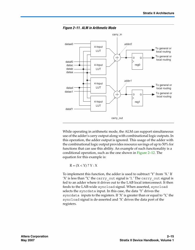
Figure 2–11. ALM in Arithmetic Mode
While operating in arithmetic mode, the ALM can support simultaneous use of the adder's carry output along with combinational logic outputs. In this operation, the adder output is ignored. This usage of the adder with the combinational logic output provides resource savings of up to 50% for functions that can use this ability. An example of such functionality is a conditional operation, such as the one shown in Figure 2–12. The equation for this example is:
R = (X < Y) ? Y : X
To implement this function, the adder is used to subtract ‘Y’ from ‘X.’ If ‘X’ is less than ‘Y,’ the carry_out signal is ‘1.’ The carry_out signal is fed to an adder where it drives out to the LAB local interconnect. It then feeds to the LAB-wide syncload signal. When asserted, syncload selects the syncdata input. In this case, the data ‘Y’ drives the syncdata inputs to the registers. If ‘X’ is greater than or equal to ‘Y,’ the syncload signal is de-asserted and ‘X’ drives the data port of the registers.
dataf0
datae0
carry_in
carry_out
dataadatabdatac
dataddatae1
dataf1
D Q
D Q
To general orlocal routing
To general orlocal routing
reg0
reg1
To general orlocal routing
To general orlocal routing
4-Input
LUT
4-Input
LUT
4-Input
LUT
4-Input
LUT
adder1
adder0
2–16 Altera CorporationStratix II Device Handbook, Volume 1 May 2007
Adaptive Logic Modules
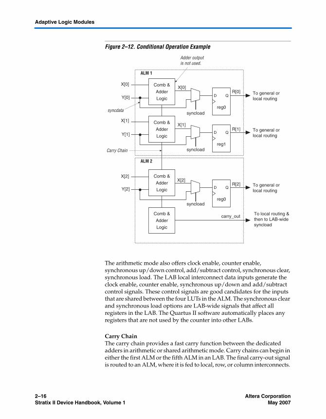
Figure 2–12. Conditional Operation Example
The arithmetic mode also offers clock enable, counter enable, synchronous up/down control, add/subtract control, synchronous clear, synchronous load. The LAB local interconnect data inputs generate the clock enable, counter enable, synchronous up/down and add/subtract control signals. These control signals are good candidates for the inputs that are shared between the four LUTs in the ALM. The synchronous clear and synchronous load options are LAB-wide signals that affect all registers in the LAB. The Quartus II software automatically places any registers that are not used by the counter into other LABs.
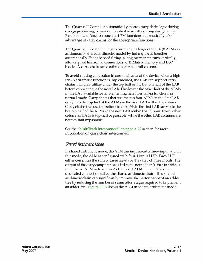
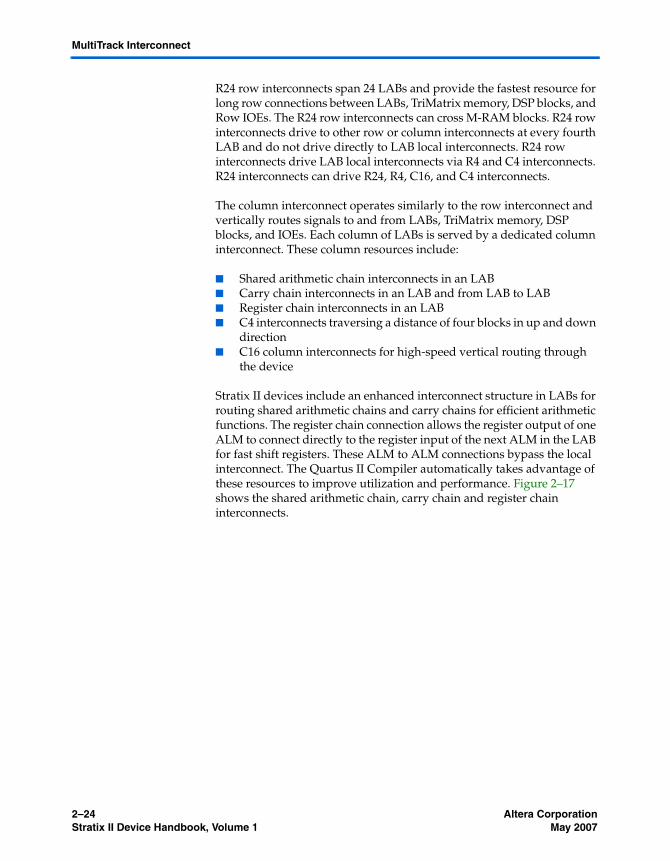
Carry ChainThe carry chain provides a fast carry function between the dedicated adders in arithmetic or shared arithmetic mode. Carry chains can begin in either the first ALM or the fifth ALM in an LAB. The final carry-out signal is routed to an ALM, where it is fed to local, row, or column interconnects.
Y[1]
Y[0]
X[0]X[0]
carry_out
X[2]X[2]
X[1]X[1]
Y[2]
D QTo general orlocal routing
reg0
Comb &
Adder
Logic
Comb &
Adder
Logic
Comb &
Adder
Logic
Comb &
Adder
Logic
D QTo general orlocal routing
reg1
D QTo general orlocal routing
To local routing &then to LAB-widesyncload
reg0
syncload
syncload
syncload
ALM 1
ALM 2
R[0]
R[1]
R[2]
Carry Chain
Adder outputis not used.
syncdata
Altera Corporation 2–17May 2007 Stratix II Device Handbook, Volume 1
Stratix II Architecture
The Quartus II Compiler automatically creates carry chain logic during design processing, or you can create it manually during design entry. Parameterized functions such as LPM functions automatically take advantage of carry chains for the appropriate functions.
The Quartus II Compiler creates carry chains longer than 16 (8 ALMs in arithmetic or shared arithmetic mode) by linking LABs together automatically. For enhanced fitting, a long carry chain runs vertically allowing fast horizontal connections to TriMatrix memory and DSP blocks. A carry chain can continue as far as a full column.
To avoid routing congestion in one small area of the device when a high fan-in arithmetic function is implemented, the LAB can support carry chains that only utilize either the top half or the bottom half of the LAB before connecting to the next LAB. This leaves the other half of the ALMs in the LAB available for implementing narrower fan-in functions in normal mode. Carry chains that use the top four ALMs in the first LAB carry into the top half of the ALMs in the next LAB within the column. Carry chains that use the bottom four ALMs in the first LAB carry into the bottom half of the ALMs in the next LAB within the column. Every other column of LABs is top-half bypassable, while the other LAB columns are bottom-half bypassable.
See the “MultiTrack Interconnect” on page 2–22 section for more information on carry chain interconnect.
Shared Arithmetic Mode
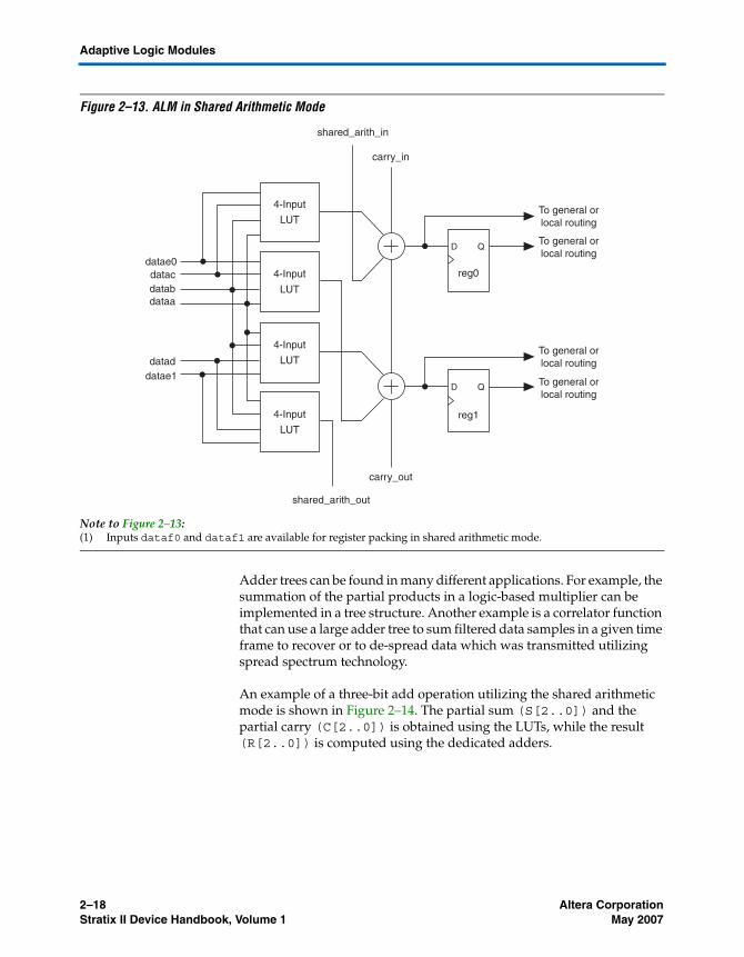
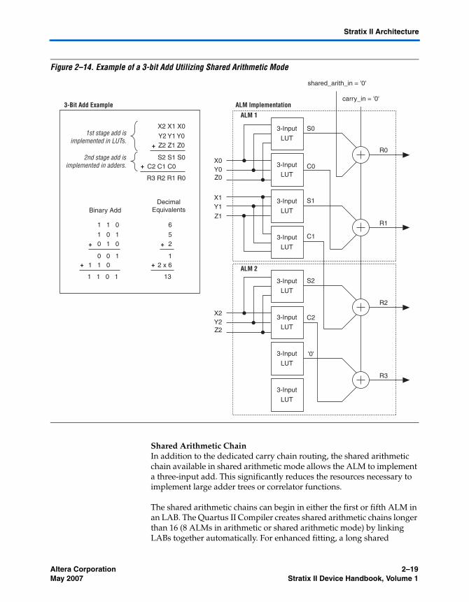
In shared arithmetic mode, the ALM can implement a three-input add. In this mode, the ALM is configured with four 4-input LUTs. Each LUT either computes the sum of three inputs or the carry of three inputs. The output of the carry computation is fed to the next adder (either to adder1 in the same ALM or to adder0 of the next ALM in the LAB) via a dedicated connection called the shared arithmetic chain. This shared arithmetic chain can significantly improve the performance of an adder tree by reducing the number of summation stages required to implement an adder tree. Figure 2–13 shows the ALM in shared arithmetic mode.
2–18 Altera CorporationStratix II Device Handbook, Volume 1 May 2007
Adaptive Logic Modules
Figure 2–13. ALM in Shared Arithmetic Mode
Note to Figure 2–13:(1) Inputs dataf0 and dataf1 are available for register packing in shared arithmetic mode.
Adder trees can be found in many different applications. For example, the summation of the partial products in a logic-based multiplier can be implemented in a tree structure. Another example is a correlator function that can use a large adder tree to sum filtered data samples in a given time frame to recover or to de-spread data which was transmitted utilizing spread spectrum technology.
An example of a three-bit add operation utilizing the shared arithmetic mode is shown in Figure 2–14. The partial sum (S[2..0]) and the partial carry (C[2..0]) is obtained using the LUTs, while the result (R[2..0]) is computed using the dedicated adders.
datae0
carry_in
shared_arith_in
shared_arith_out
carry_out
dataadatabdatac
dataddatae1
D Q
D Q
To general orlocal routing
To general orlocal routing
reg0
reg1
To general orlocal routing
To general orlocal routing
4-Input
LUT
4-Input
LUT
4-Input
LUT
4-Input
LUT
Altera Corporation 2–19May 2007 Stratix II Device Handbook, Volume 1
Stratix II Architecture
Figure 2–14. Example of a 3-bit Add Utilizing Shared Arithmetic Mode
Shared Arithmetic ChainIn addition to the dedicated carry chain routing, the shared arithmetic chain available in shared arithmetic mode allows the ALM to implement a three-input add. This significantly reduces the resources necessary to implement large adder trees or correlator functions.
The shared arithmetic chains can begin in either the first or fifth ALM in an LAB. The Quartus II Compiler creates shared arithmetic chains longer than 16 (8 ALMs in arithmetic or shared arithmetic mode) by linking LABs together automatically. For enhanced fitting, a long shared
carry_in = '0'
shared_arith_in = '0'
Z0Y0X0
Binary AddDecimal
Equivalents
+
Z1
X1
R0
C0
S0
S1
S2
C1
C2
'0'
R1
Y1
3-Input
LUT
3-Input
LUT
3-Input
LUT
3-Input
LUT
Z2Y2X2
R2
R3
3-Input
LUT
3-Input
LUT
3-Input
LUT
3-Input
LUT
ALM 1
3-Bit Add Example ALM Implementation
ALM 2
X2 X1 X0
Y2 Y1 Y0Z2 Z1 Z0
S2 S1 S0C2 C1 C0
R3 R2 R1 R0
+
+
1 1 0
1 0 10 1 0
0 0 11 1 0
1 1 0 1
+
+
6
52
12 x 6
13
+
2nd stage add isimplemented in adders.
1st stage add isimplemented in LUTs.
2–20 Altera CorporationStratix II Device Handbook, Volume 1 May 2007
Adaptive Logic Modules
arithmetic chain runs vertically allowing fast horizontal connections to TriMatrix memory and DSP blocks. A shared arithmetic chain can continue as far as a full column.
Similar to the carry chains, the shared arithmetic chains are also top- or bottom-half bypassable. This capability allows the shared arithmetic chain to cascade through half of the ALMs in a LAB while leaving the other half available for narrower fan-in functionality. Every other LAB column is top-half bypassable, while the other LAB columns are bottom-half bypassable.
See the “MultiTrack Interconnect” on page 2–22 section for more information on shared arithmetic chain interconnect.
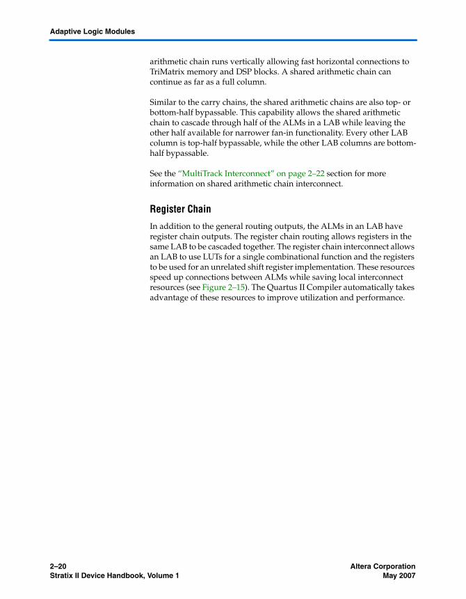
Register Chain
In addition to the general routing outputs, the ALMs in an LAB have register chain outputs. The register chain routing allows registers in the same LAB to be cascaded together. The register chain interconnect allows an LAB to use LUTs for a single combinational function and the registers to be used for an unrelated shift register implementation. These resources speed up connections between ALMs while saving local interconnect resources (see Figure 2–15). The Quartus II Compiler automatically takes advantage of these resources to improve utilization and performance.
Altera Corporation 2–21May 2007 Stratix II Device Handbook, Volume 1
Stratix II Architecture
Figure 2–15. Register Chain within an LAB Note (1)
Note to Figure 2–15:(1) The combinational or adder logic can be utilized to implement an unrelated, un-registered function.
See the “MultiTrack Interconnect” on page 2–22 section for more information on register chain interconnect.
D QTo general orlocal routing
reg0
To general orlocal routing
reg_chain_in
adder0
D QTo general orlocal routing
reg1
To general orlocal routing
adder1
D QTo general orlocal routing
reg0
To general orlocal routing
reg_chain_out
adder0
D QTo general orlocal routing
reg1
To general orlocal routing
adder1
From Previous ALMWithin The LAB
To Next ALMwithin the LAB
Combinational
Logic
CombinationalLogic
2–22 Altera CorporationStratix II Device Handbook, Volume 1 May 2007
MultiTrack Interconnect
Clear & Preset Logic Control
LAB-wide signals control the logic for the register's clear and load/preset signals. The ALM directly supports an asynchronous clear and preset function. The register preset is achieved through the asynchronous load of a logic high. The direct asynchronous preset does not require a NOT-gate push-back technique. Stratix II devices support simultaneous asynchronous load/preset, and clear signals. An asynchronous clear signal takes precedence if both signals are asserted simultaneously. Each LAB supports up to two clears and one load/preset signal.
In addition to the clear and load/preset ports, Stratix II devices provide a device-wide reset pin (DEV_CLRn) that resets all registers in the device. An option set before compilation in the Quartus II software controls this pin. This device-wide reset overrides all other control signals.
MultiTrack Interconnect
In the Stratix II architecture, connections between ALMs, TriMatrix memory, DSP blocks, and device I/O pins are provided by the MultiTrack interconnect structure with DirectDriveTM technology. The MultiTrack interconnect consists of continuous, performance-optimized routing lines of different lengths and speeds used for inter- and intra-design block connectivity. The Quartus II Compiler automatically places critical design paths on faster interconnects to improve design performance.
DirectDrive technology is a deterministic routing technology that ensures identical routing resource usage for any function regardless of placement in the device. The MultiTrack interconnect and DirectDrive technology simplify the integration stage of block-based designing by eliminating the re-optimization cycles that typically follow design changes and additions.
The MultiTrack interconnect consists of row and column interconnects that span fixed distances. A routing structure with fixed length resources for all devices allows predictable and repeatable performance when migrating through different device densities. Dedicated row interconnects route signals to and from LABs, DSP blocks, and TriMatrix memory in the same row. These row resources include:
■ Direct link interconnects between LABs and adjacent blocks■ R4 interconnects traversing four blocks to the right or left■ R24 row interconnects for high-speed access across the length of the
device
Altera Corporation 2–23May 2007 Stratix II Device Handbook, Volume 1
Stratix II Architecture
The direct link interconnect allows an LAB, DSP block, or TriMatrix memory block to drive into the local interconnect of its left and right neighbors and then back into itself. This provides fast communication between adjacent LABs and/or blocks without using row interconnect resources.
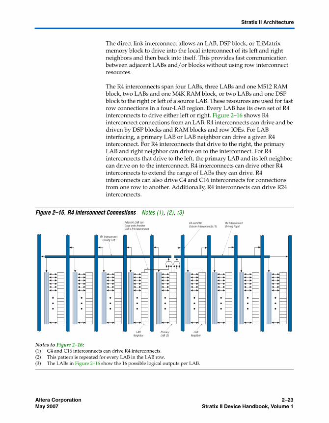
The R4 interconnects span four LABs, three LABs and one M512 RAM block, two LABs and one M4K RAM block, or two LABs and one DSP block to the right or left of a source LAB. These resources are used for fast row connections in a four-LAB region. Every LAB has its own set of R4 interconnects to drive either left or right. Figure 2–16 shows R4 interconnect connections from an LAB. R4 interconnects can drive and be driven by DSP blocks and RAM blocks and row IOEs. For LAB interfacing, a primary LAB or LAB neighbor can drive a given R4 interconnect. For R4 interconnects that drive to the right, the primary LAB and right neighbor can drive on to the interconnect. For R4 interconnects that drive to the left, the primary LAB and its left neighbor can drive on to the interconnect. R4 interconnects can drive other R4 interconnects to extend the range of LABs they can drive. R4 interconnects can also drive C4 and C16 interconnects for connections from one row to another. Additionally, R4 interconnects can drive R24 interconnects.
Figure 2–16. R4 Interconnect Connections Notes (1), (2), (3)
Notes to Figure 2–16:(1) C4 and C16 interconnects can drive R4 interconnects.(2) This pattern is repeated for every LAB in the LAB row.(3) The LABs in Figure 2–16 show the 16 possible logical outputs per LAB.
PrimaryLAB (2)
R4 InterconnectDriving Left
Adjacent LAB canDrive onto AnotherLAB's R4 Interconnect
C4 and C16Column Interconnects (1)
R4 InterconnectDriving Right
LABNeighbor
LABNeighbor
2–24 Altera CorporationStratix II Device Handbook, Volume 1 May 2007
MultiTrack Interconnect
R24 row interconnects span 24 LABs and provide the fastest resource for long row connections between LABs, TriMatrix memory, DSP blocks, and Row IOEs. The R24 row interconnects can cross M-RAM blocks. R24 row interconnects drive to other row or column interconnects at every fourth LAB and do not drive directly to LAB local interconnects. R24 row interconnects drive LAB local interconnects via R4 and C4 interconnects. R24 interconnects can drive R24, R4, C16, and C4 interconnects.
The column interconnect operates similarly to the row interconnect and vertically routes signals to and from LABs, TriMatrix memory, DSP blocks, and IOEs. Each column of LABs is served by a dedicated column interconnect. These column resources include:
■ Shared arithmetic chain interconnects in an LAB■ Carry chain interconnects in an LAB and from LAB to LAB■ Register chain interconnects in an LAB■ C4 interconnects traversing a distance of four blocks in up and down
direction■ C16 column interconnects for high-speed vertical routing through
the device
Stratix II devices include an enhanced interconnect structure in LABs for routing shared arithmetic chains and carry chains for efficient arithmetic functions. The register chain connection allows the register output of one ALM to connect directly to the register input of the next ALM in the LAB for fast shift registers. These ALM to ALM connections bypass the local interconnect. The Quartus II Compiler automatically takes advantage of these resources to improve utilization and performance. Figure 2–17 shows the shared arithmetic chain, carry chain and register chain interconnects.
Altera Corporation 2–25May 2007 Stratix II Device Handbook, Volume 1
Stratix II Architecture
Figure 2–17. Shared Arithmetic Chain, Carry Chain & Register Chain Interconnects
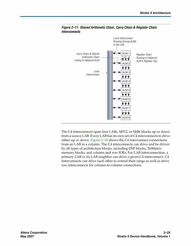
The C4 interconnects span four LABs, M512, or M4K blocks up or down from a source LAB. Every LAB has its own set of C4 interconnects to drive either up or down. Figure 2–18 shows the C4 interconnect connections from an LAB in a column. The C4 interconnects can drive and be driven by all types of architecture blocks, including DSP blocks, TriMatrix memory blocks, and column and row IOEs. For LAB interconnection, a primary LAB or its LAB neighbor can drive a given C4 interconnect. C4 interconnects can drive each other to extend their range as well as drive row interconnects for column-to-column connections.
ALM 1
ALM 2
ALM 3
ALM 4
ALM 5
ALM 6
ALM 8
ALM 7
Carry Chain & SharedArithmetic Chain
Routing to Adjacent ALM
LocalInterconnect
Register ChainRouting to AdjacentALM's Register Inpu
Local InterconnectRouting Among ALMsin the LAB
2–26 Altera CorporationStratix II Device Handbook, Volume 1 May 2007
MultiTrack Interconnect
Figure 2–18. C4 Interconnect Connections Note (1)
Note to Figure 2–18:(1) Each C4 interconnect can drive either up or down four rows.
C4 InterconnectDrives Local and R4Interconnectsup to Four Rows
Adjacent LAB candrive onto neighboringLAB's C4 interconnect
C4 InterconnectDriving Up
C4 InterconnectDriving Down
LAB
RowInterconnect
LocalInterconnect
Altera Corporation 2–27May 2007 Stratix II Device Handbook, Volume 1
Stratix II Architecture
C16 column interconnects span a length of 16 LABs and provide the fastest resource for long column connections between LABs, TriMatrix memory blocks, DSP blocks, and IOEs. C16 interconnects can cross M-RAM blocks and also drive to row and column interconnects at every fourth LAB. C16 interconnects drive LAB local interconnects via C4 and R4 interconnects and do not drive LAB local interconnects directly.
All embedded blocks communicate with the logic array similar to LAB-to-LAB interfaces. Each block (that is, TriMatrix memory and DSP blocks) connects to row and column interconnects and has local interconnect regions driven by row and column interconnects. These blocks also have direct link interconnects for fast connections to and from a neighboring LAB. All blocks are fed by the row LAB clocks, labclk[5..0].
Table 2–2 shows the Stratix II device’s routing scheme.
Table 2–2. Stratix II Device Routing Scheme (Part 1 of 2)
Source
Destination
Shar
ed A
rithm
etic
Cha
in
Carr
y Ch
ain
Regi
ster
Cha
in
Loca
l Int
erco
nnec
t
Dire
ct L
ink
Inte
rcon
nect
R4 In
terc
onne
ct
R24
Inte
rcon
nect
C4 In
terc
onne
ct
C16
Inte
rcon
nect
ALM
M51
2 RA
M B
lock
M4K
RAM
Blo
ck
M-R
AM B
lock
DSP
Bloc
ks
Colu
mn
IOE
Row
IOE
Shared arithmetic chain v
Carry chain v
Register chain v
Local interconnect v v v v v v v
Direct link interconnect v
R4 interconnect v v v v v
R24 interconnect v v v v
C4 interconnect v v v
C16 interconnect v v v v
ALM v v v v v v v
M512 RAM block v v v v
M4K RAM block v v v v
M-RAM block v v v v
DSP blocks v v v
2–28 Altera CorporationStratix II Device Handbook, Volume 1 May 2007
TriMatrix Memory
TriMatrix Memory
TriMatrix memory consists of three types of RAM blocks: M512, M4K, and M-RAM. Although these memory blocks are different, they can all implement various types of memory with or without parity, including true dual-port, simple dual-port, and single-port RAM, ROM, and FIFO buffers. Table 2–3 shows the size and features of the different RAM blocks.
Column IOE v v v
Row IOE v v v v
Table 2–2. Stratix II Device Routing Scheme (Part 2 of 2)
Source
Destination
Shar
ed A
rithm
etic
Cha
in
Carr
y Ch
ain
Regi
ster
Cha
in
Loca
l Int
erco
nnec
t
Dire
ct L
ink
Inte
rcon
nect
R4 In
terc
onne
ct
R24
Inte
rcon
nect
C4 In
terc
onne
ct
C16
Inte
rcon
nect
ALM
M51
2 RA
M B
lock
M4K
RAM
Blo
ck
M-R
AM B
lock
DSP
Bloc
ks
Colu
mn
IOE
Row
IOE
Table 2–3. TriMatrix Memory Features (Part 1 of 2)
Memory Feature M512 RAM Block (32 × 18 Bits)
M4K RAM Block (128 × 36 Bits)
M-RAM Block (4K × 144 Bits)
Maximum performance 500 MHz 550 MHz 420 MHz
True dual-port memory v v
Simple dual-port memory v v v
Single-port memory v v v
Shift register v v
ROM v v (1)
FIFO buffer v v v
Pack mode v v
Byte enable v v v
Address clock enable v v
Parity bits v v v
Mixed clock mode v v v
Memory initialization (.mif) v v
Altera Corporation 2–29May 2007 Stratix II Device Handbook, Volume 1
Stratix II Architecture
Memory Block Size
TriMatrix memory provides three different memory sizes for efficient application support. The Quartus II software automatically partitions the user-defined memory into the embedded memory blocks using the most efficient size combinations. You can also manually assign the memory to a specific block size or a mixture of block sizes.
When applied to input registers, the asynchronous clear signal for the TriMatrix embedded memory immediately clears the input registers. However, the output of the memory block does not show the effects until the next clock edge. When applied to output registers, the asynchronous clear signal clears the output registers and the effects are seen immediately.
Simple dual-port memory mixed width support
v v v
True dual-port memory mixed width support
v v
Power-up conditions Outputs cleared Outputs cleared Outputs unknown
Register clears Output registers Output registers Output registers
Mixed-port read-during-write Unknown output/old data Unknown output/old data Unknown output
Configurations 512 × 1256 × 2128 × 464 × 864 × 932 × 1632 × 18
4K × 12K × 21K × 4512 × 8512 × 9256 × 16256 × 18128 × 32128 × 36
64K × 864K × 932K × 1632K × 1816K × 3216K × 368K × 648K × 724K × 1284K × 144
Notes to Table 2–3:(1) The M-RAM block does not support memory initializations. However, the M-RAM block can emulate a ROM
function using a dual-port RAM bock. The Stratix II device must write to the dual-port memory once and then disable the write-enable ports afterwards.
Table 2–3. TriMatrix Memory Features (Part 2 of 2)
Memory Feature M512 RAM Block (32 × 18 Bits)
M4K RAM Block (128 × 36 Bits)
M-RAM Block (4K × 144 Bits)
2–30 Altera CorporationStratix II Device Handbook, Volume 1 May 2007
TriMatrix Memory
M512 RAM Block
The M512 RAM block is a simple dual-port memory block and is useful for implementing small FIFO buffers, DSP, and clock domain transfer applications. Each block contains 576 RAM bits (including parity bits). M512 RAM blocks can be configured in the following modes:
■ Simple dual-port RAM■ Single-port RAM■ FIFO■ ROM■ Shift register
1 Violating the setup or hold time on the memory block address registers could corrupt memory contents. This applies to both read and write operations.
When configured as RAM or ROM, you can use an initialization file to pre-load the memory contents.
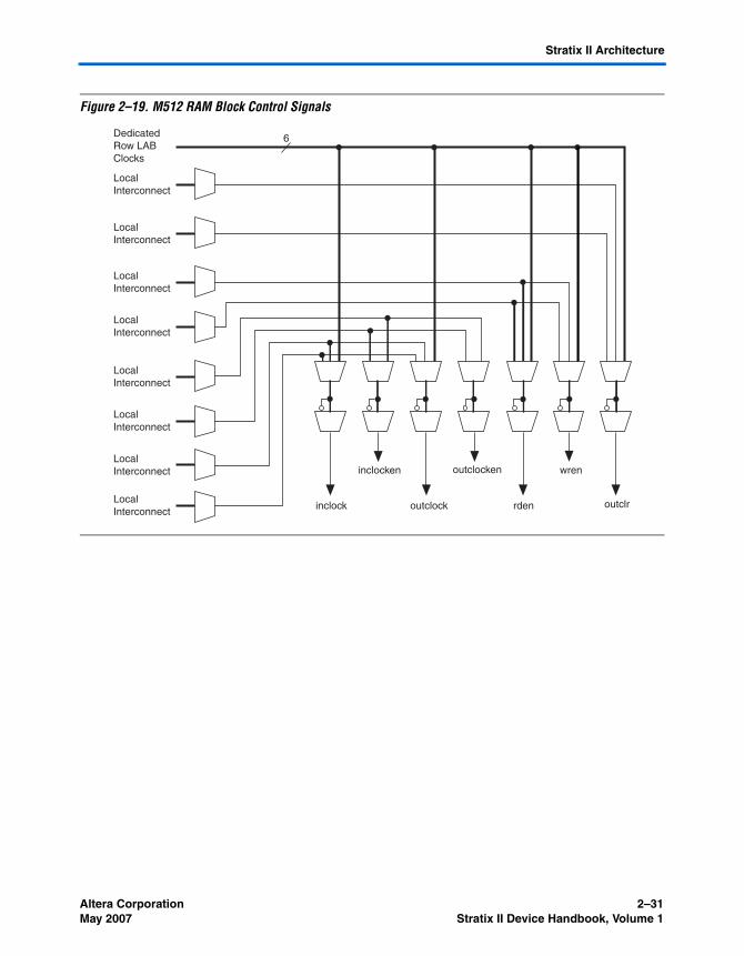
M512 RAM blocks can have different clocks on its inputs and outputs. The wren, datain, and write address registers are all clocked together from one of the two clocks feeding the block. The read address, rden, and output registers can be clocked by either of the two clocks driving the block. This allows the RAM block to operate in read/write or input/output clock modes. Only the output register can be bypassed. The six labclk signals or local interconnect can drive the inclock, outclock, wren, rden, and outclr signals. Because of the advanced interconnect between the LAB and M512 RAM blocks, ALMs can also control the wren and rden signals and the RAM clock, clock enable, and asynchronous clear signals. Figure 2–19 shows the M512 RAM block control signal generation logic.
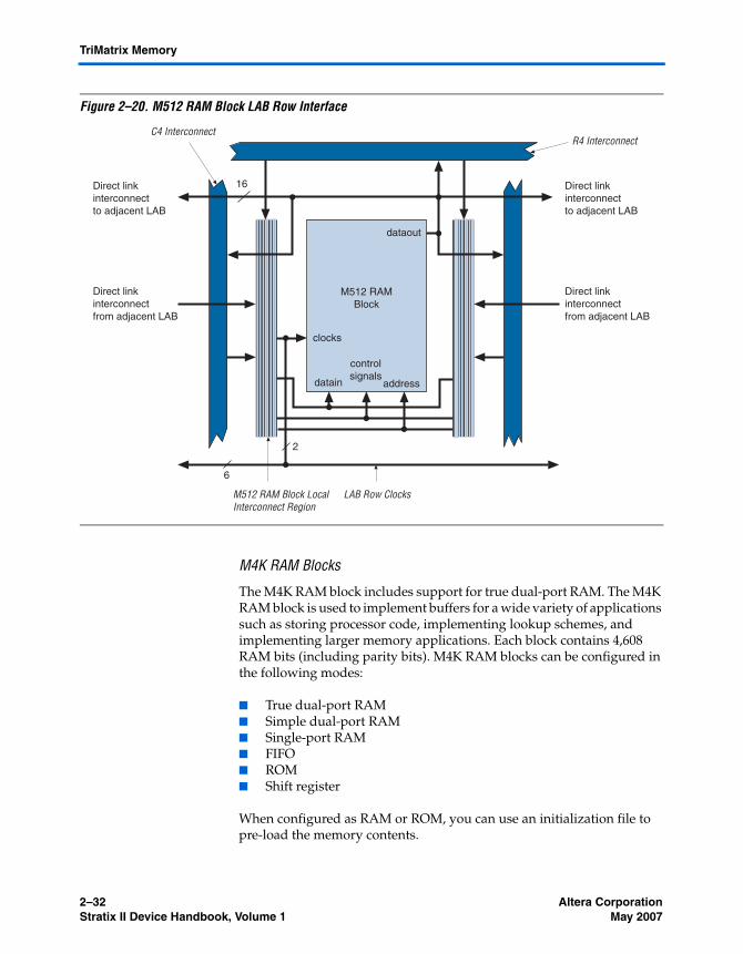
The RAM blocks in Stratix II devices have local interconnects to allow ALMs and interconnects to drive into RAM blocks. The M512 RAM block local interconnect is driven by the R4, C4, and direct link interconnects from adjacent LABs. The M512 RAM blocks can communicate with LABs on either the left or right side through these row interconnects or with LAB columns on the left or right side with the column interconnects. The M512 RAM block has up to 16 direct link input connections from the left adjacent LABs and another 16 from the right adjacent LAB. M512 RAM outputs can also connect to left and right LABs through direct link interconnect. The M512 RAM block has equal opportunity for access and performance to and from LABs on either its left or right side. Figure 2–20 shows the M512 RAM block to logic array interface.
Altera Corporation 2–31May 2007 Stratix II Device Handbook, Volume 1
Stratix II Architecture
Figure 2–19. M512 RAM Block Control Signals
inclocken
outclockinclock
outclocken
rden
wren
DedicatedRow LABClocks
LocalInterconnect
LocalInterconnect
LocalInterconnect
LocalInterconnect
LocalInterconnect
LocalInterconnect
outclr
6
LocalInterconnect
LocalInterconnect
2–32 Altera CorporationStratix II Device Handbook, Volume 1 May 2007
TriMatrix Memory
Figure 2–20. M512 RAM Block LAB Row Interface
M4K RAM Blocks
The M4K RAM block includes support for true dual-port RAM. The M4K RAM block is used to implement buffers for a wide variety of applications such as storing processor code, implementing lookup schemes, and implementing larger memory applications. Each block contains 4,608 RAM bits (including parity bits). M4K RAM blocks can be configured in the following modes:
■ True dual-port RAM■ Simple dual-port RAM■ Single-port RAM■ FIFO■ ROM■ Shift register
When configured as RAM or ROM, you can use an initialization file to pre-load the memory contents.
dataout
M512 RAMBlock
datain
clocks
16
Direct link interconnectfrom adjacent LAB
Direct link interconnectto adjacent LAB
Direct link interconnectfrom adjacent LAB
Direct link interconnectto adjacent LAB
M512 RAM Block LocalInterconnect Region
C4 InterconnectR4 Interconnect
controlsignals
address
LAB Row Clocks
2
6
Altera Corporation 2–33May 2007 Stratix II Device Handbook, Volume 1
Stratix II Architecture
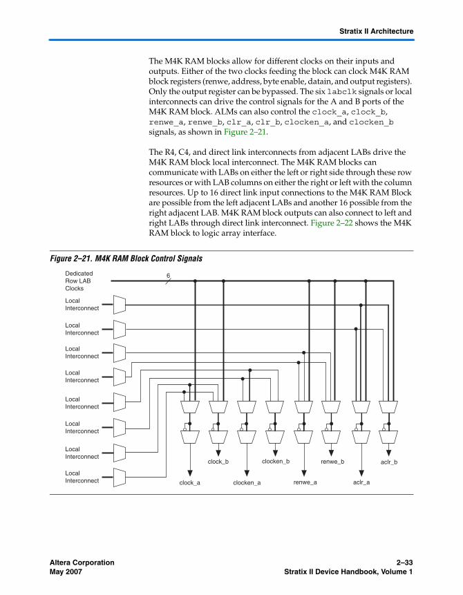
The M4K RAM blocks allow for different clocks on their inputs and outputs. Either of the two clocks feeding the block can clock M4K RAM block registers (renwe, address, byte enable, datain, and output registers). Only the output register can be bypassed. The six labclk signals or local interconnects can drive the control signals for the A and B ports of the M4K RAM block. ALMs can also control the clock_a, clock_b, renwe_a, renwe_b, clr_a, clr_b, clocken_a, and clocken_b signals, as shown in Figure 2–21.
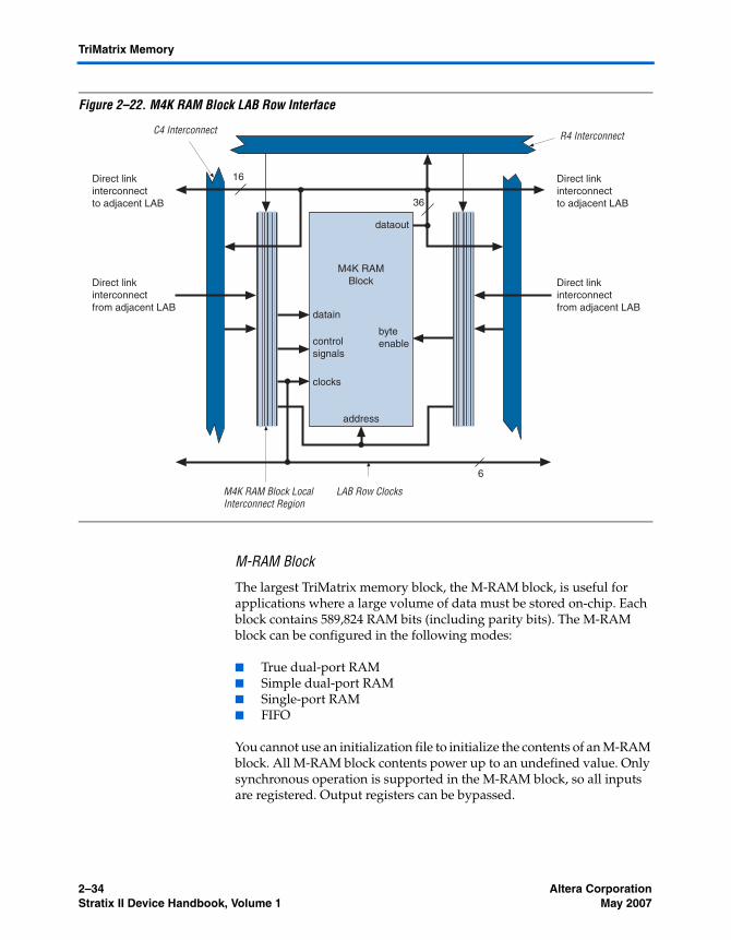
The R4, C4, and direct link interconnects from adjacent LABs drive the M4K RAM block local interconnect. The M4K RAM blocks can communicate with LABs on either the left or right side through these row resources or with LAB columns on either the right or left with the column resources. Up to 16 direct link input connections to the M4K RAM Block are possible from the left adjacent LABs and another 16 possible from the right adjacent LAB. M4K RAM block outputs can also connect to left and right LABs through direct link interconnect. Figure 2–22 shows the M4K RAM block to logic array interface.
Figure 2–21. M4K RAM Block Control Signals
clock_b
clocken_aclock_a
clocken_b aclr_b
aclr_a
DedicatedRow LABClocks
LocalInterconnect
LocalInterconnect
LocalInterconnect
LocalInterconnect
LocalInterconnect
LocalInterconnect
LocalInterconnect
LocalInterconnect
renwe_b
renwe_a
6
2–34 Altera CorporationStratix II Device Handbook, Volume 1 May 2007
TriMatrix Memory
Figure 2–22. M4K RAM Block LAB Row Interface
M-RAM Block
The largest TriMatrix memory block, the M-RAM block, is useful for applications where a large volume of data must be stored on-chip. Each block contains 589,824 RAM bits (including parity bits). The M-RAM block can be configured in the following modes:
■ True dual-port RAM■ Simple dual-port RAM■ Single-port RAM■ FIFO
You cannot use an initialization file to initialize the contents of an M-RAM block. All M-RAM block contents power up to an undefined value. Only synchronous operation is supported in the M-RAM block, so all inputs are registered. Output registers can be bypassed.
dataout
M4K RAMBlock
datain
address
16
36
Direct link interconnectfrom adjacent LAB
Direct link interconnectto adjacent LAB
Direct link interconnectfrom adjacent LAB
Direct link interconnectto adjacent LAB
M4K RAM Block LocalInterconnect Region
C4 Interconnect R4 Interconnect
LAB Row Clocks
clocks
byteenablecontrol
signals
6
Altera Corporation 2–35May 2007 Stratix II Device Handbook, Volume 1
Stratix II Architecture
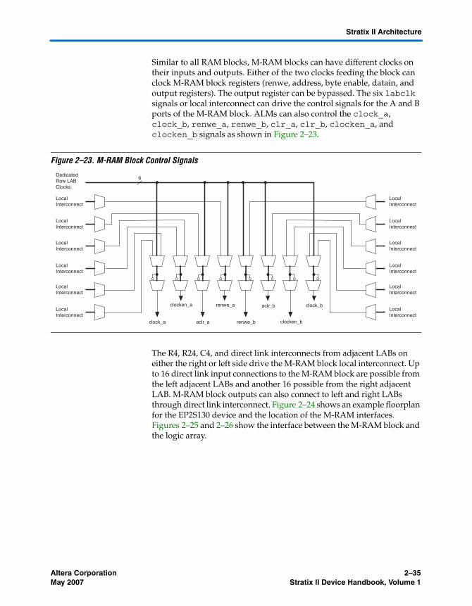
Similar to all RAM blocks, M-RAM blocks can have different clocks on their inputs and outputs. Either of the two clocks feeding the block can clock M-RAM block registers (renwe, address, byte enable, datain, and output registers). The output register can be bypassed. The six labclk signals or local interconnect can drive the control signals for the A and B ports of the M-RAM block. ALMs can also control the clock_a, clock_b, renwe_a, renwe_b, clr_a, clr_b, clocken_a, and clocken_b signals as shown in Figure 2–23.
Figure 2–23. M-RAM Block Control Signals
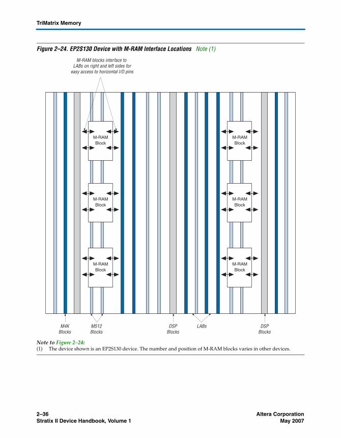
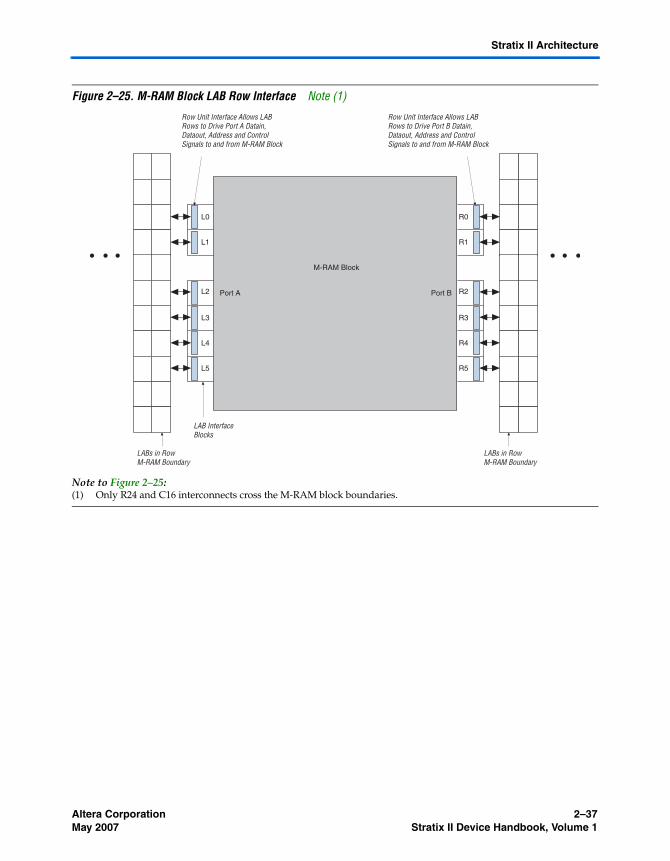
The R4, R24, C4, and direct link interconnects from adjacent LABs on either the right or left side drive the M-RAM block local interconnect. Up to 16 direct link input connections to the M-RAM block are possible from the left adjacent LABs and another 16 possible from the right adjacent LAB. M-RAM block outputs can also connect to left and right LABs through direct link interconnect. Figure 2–24 shows an example floorplan for the EP2S130 device and the location of the M-RAM interfaces. Figures 2–25 and 2–26 show the interface between the M-RAM block and the logic array.
clock_a
clock_bclocken_a
clocken_baclr_a
aclr_b
DedicatedRow LABClocks
LocalInterconnect
LocalInterconnect
LocalInterconnect
LocalInterconnect
renwe_a
renwe_b
6
LocalInterconnect
LocalInterconnect
LocalInterconnect
LocalInterconnect
LocalInterconnect
LocalInterconnect
LocalInterconnect
LocalInterconnect
2–36 Altera CorporationStratix II Device Handbook, Volume 1 May 2007
TriMatrix Memory
Figure 2–24. EP2S130 Device with M-RAM Interface Locations Note (1)
Note to Figure 2–24:(1) The device shown is an EP2S130 device. The number and position of M-RAM blocks varies in other devices.
DSPBlocks
DSPBlocks
M4KBlocks
M512Blocks
LABs
M-RAMBlock
M-RAMBlock
M-RAMBlock
M-RAMBlock
M-RAMBlock
M-RAMBlock
M-RAM blocks interface to LABs on right and left sides for
easy access to horizontal I/O pins
Altera Corporation 2–37May 2007 Stratix II Device Handbook, Volume 1
Stratix II Architecture
Figure 2–25. M-RAM Block LAB Row Interface Note (1)
Note to Figure 2–25:(1) Only R24 and C16 interconnects cross the M-RAM block boundaries.
M-RAM Block
Port BPort A
Row Unit Interface Allows LABRows to Drive Port B Datain,Dataout, Address and ControlSignals to and from M-RAM Block
Row Unit Interface Allows LABRows to Drive Port A Datain,Dataout, Address and ControlSignals to and from M-RAM Block
LABs in RowM-RAM Boundary
LABs in RowM-RAM Boundary
LAB InterfaceBlocks
L0
L1
L2
L3
L4
L5
R0
R1
R2
R3
R4
R5
2–38 Altera CorporationStratix II Device Handbook, Volume 1 May 2007
TriMatrix Memory
Figure 2–26. M-RAM Row Unit Interface to Interconnect
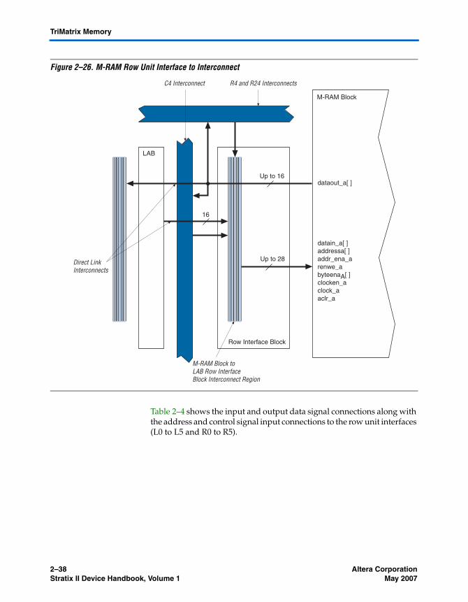
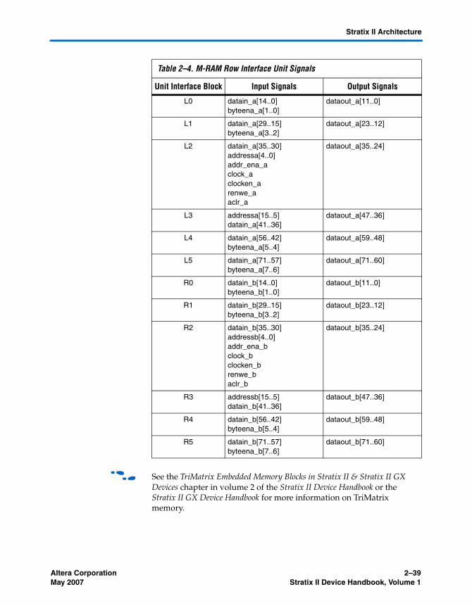
Table 2–4 shows the input and output data signal connections along with the address and control signal input connections to the row unit interfaces (L0 to L5 and R0 to R5).
LAB
Row Interface Block
M-RAM Block
16
Up to 28
datain_a[ ]addressa[ ]addr_ena_arenwe_abyteenaA[ ]clocken_aclock_aaclr_a
M-RAM Block toLAB Row InterfaceBlock Interconnect Region
R4 and R24 InterconnectsC4 Interconnect
Direct LinkInterconnects
dataout_a[ ]Up to 16
Altera Corporation 2–39May 2007 Stratix II Device Handbook, Volume 1
Stratix II Architecture
f See the TriMatrix Embedded Memory Blocks in Stratix II & Stratix II GX Devices chapter in volume 2 of the Stratix II Device Handbook or the Stratix II GX Device Handbook for more information on TriMatrix memory.
Table 2–4. M-RAM Row Interface Unit Signals
Unit Interface Block Input Signals Output Signals
L0 datain_a[14..0]byteena_a[1..0]
dataout_a[11..0]
L1 datain_a[29..15]byteena_a[3..2]
dataout_a[23..12]
L2 datain_a[35..30]addressa[4..0]addr_ena_aclock_aclocken_arenwe_aaclr_a
dataout_a[35..24]
L3 addressa[15..5]datain_a[41..36]
dataout_a[47..36]
L4 datain_a[56..42]byteena_a[5..4]
dataout_a[59..48]
L5 datain_a[71..57]byteena_a[7..6]
dataout_a[71..60]
R0 datain_b[14..0]byteena_b[1..0]
dataout_b[11..0]
R1 datain_b[29..15]byteena_b[3..2]
dataout_b[23..12]
R2 datain_b[35..30]addressb[4..0]addr_ena_bclock_bclocken_brenwe_baclr_b
dataout_b[35..24]
R3 addressb[15..5]datain_b[41..36]
dataout_b[47..36]
R4 datain_b[56..42]byteena_b[5..4]
dataout_b[59..48]
R5 datain_b[71..57]byteena_b[7..6]
dataout_b[71..60]
2–40 Altera CorporationStratix II Device Handbook, Volume 1 May 2007
Digital Signal Processing Block
Digital Signal Processing Block
The most commonly used DSP functions are FIR filters, complex FIR filters, IIR filters, fast Fourier transform (FFT) functions, direct cosine transform (DCT) functions, and correlators. All of these use the multiplier as the fundamental building block. Additionally, some applications need specialized operations such as multiply-add and multiply-accumulate operations. Stratix II devices provide DSP blocks to meet the arithmetic requirements of these functions.
Each Stratix II device has from two to four columns of DSP blocks to efficiently implement DSP functions faster than ALM-based implementations. Stratix II devices have up to 24 DSP blocks per column (see Table 2–5). Each DSP block can be configured to support up to:
■ Eight 9 × 9-bit multipliers■ Four 18 × 18-bit multipliers■ One 36 × 36-bit multiplier
As indicated, the Stratix II DSP block can support one 36 × 36-bit multiplier in a single DSP block. This is true for any combination of signed, unsigned, or mixed sign multiplications.
1 This list only shows functions that can fit into a single DSP block. Multiple DSP blocks can support larger multiplication functions.
Altera Corporation 2–41May 2007 Stratix II Device Handbook, Volume 1
Stratix II Architecture
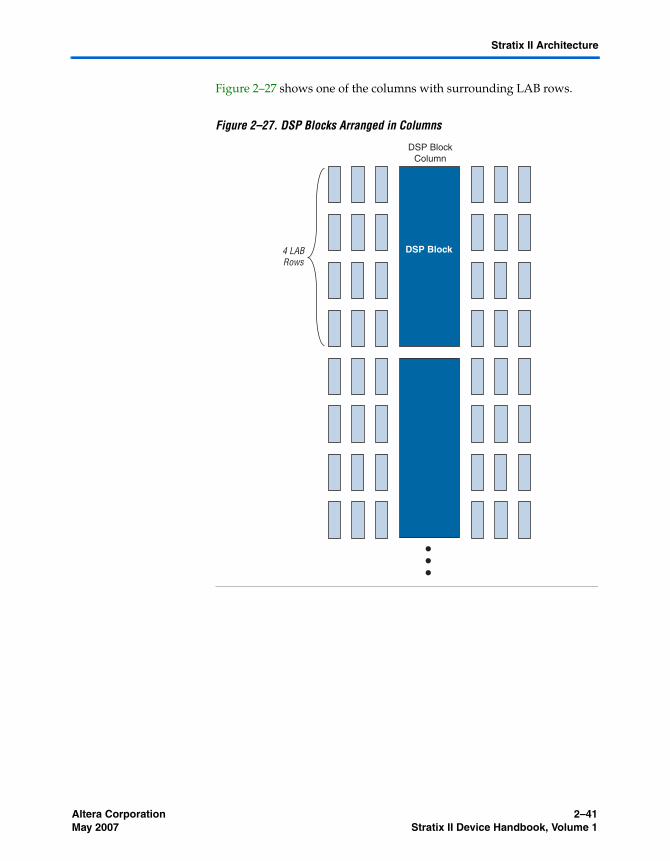
Figure 2–27 shows one of the columns with surrounding LAB rows.
Figure 2–27. DSP Blocks Arranged in Columns
DSP BlockColumn
4 LABRows
DSP Block
2–42 Altera CorporationStratix II Device Handbook, Volume 1 May 2007
Digital Signal Processing Block
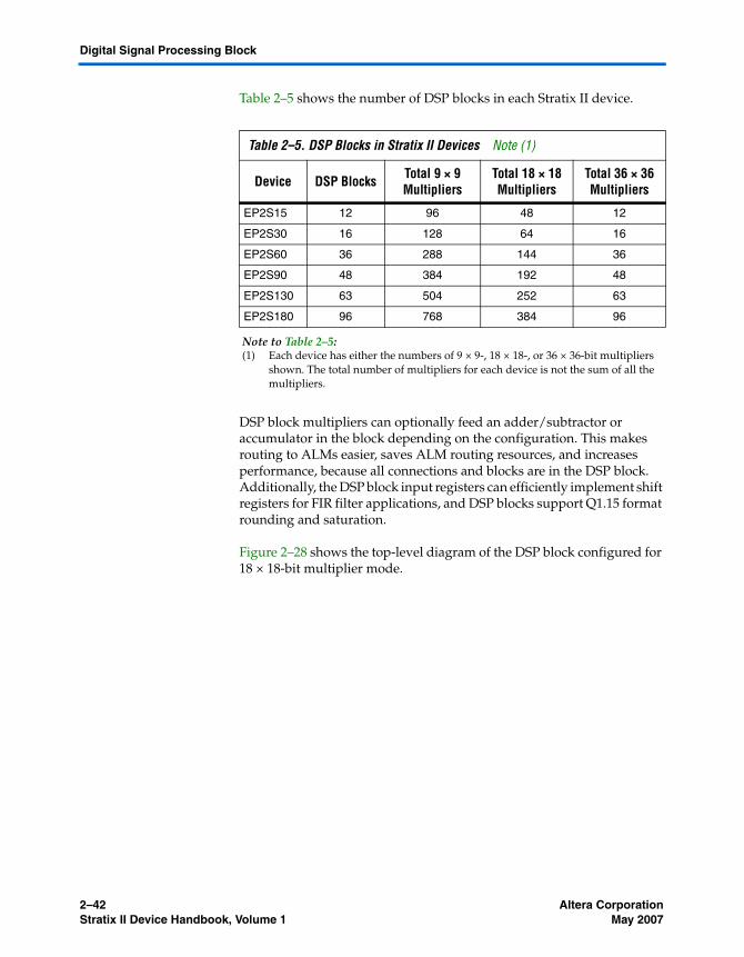
Table 2–5 shows the number of DSP blocks in each Stratix II device.
DSP block multipliers can optionally feed an adder/subtractor or accumulator in the block depending on the configuration. This makes routing to ALMs easier, saves ALM routing resources, and increases performance, because all connections and blocks are in the DSP block. Additionally, the DSP block input registers can efficiently implement shift registers for FIR filter applications, and DSP blocks support Q1.15 format rounding and saturation.
Figure 2–28 shows the top-level diagram of the DSP block configured for 18 × 18-bit multiplier mode.
Table 2–5. DSP Blocks in Stratix II Devices Note (1)
Device DSP Blocks Total 9 × 9 Multipliers
Total 18 × 18 Multipliers
Total 36 × 36 Multipliers
EP2S15 12 96 48 12
EP2S30 16 128 64 16
EP2S60 36 288 144 36
EP2S90 48 384 192 48
EP2S130 63 504 252 63
EP2S180 96 768 384 96
Note to Table 2–5:(1) Each device has either the numbers of 9 × 9-, 18 × 18-, or 36 × 36-bit multipliers
shown. The total number of multipliers for each device is not the sum of all the multipliers.
Altera Corporation 2–43May 2007 Stratix II Device Handbook, Volume 1
Stratix II Architecture
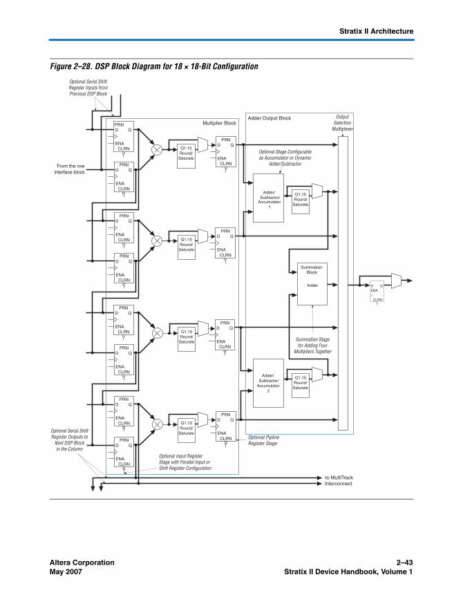
Figure 2–28. DSP Block Diagram for 18 × 18-Bit Configuration
Adder/Subtractor/
Accumulator1
Adder
Multiplier BlockPRN
CLRN
D Q
ENA
PRN
CLRN
D Q
ENA
PRN
CLRN
D Q
ENA
PRN
CLRN
D Q
ENA
PRN
CLRN
D Q
ENA
PRN
CLRN
D Q
ENA
PRN
CLRN
D Q
ENA
PRN
CLRN
D Q
ENA
PRN
CLRN
D Q
ENA
PRN
CLRN
D Q
ENA
PRN
CLRN
D Q
ENA
PRN
CLRN
D Q
ENA
SummationBlock
Adder Output Block
Adder/Subtractor/
Accumulator2
Q1.15Round/
Saturate
Q1.15Round/
Saturate
Q1.15Round/
Saturate
Q1.15Round/
Saturate
to MultiTrackInterconnect
CLRN
D QENA
From the rowinterface block
Optional Serial ShiftRegister Inputs fromPrevious DSP Block
Optional Serial ShiftRegister Outputs to
Next DSP Blockin the Column
Optional Input RegisterStage with Parallel Input orShift Register Configuration
Optional PiplineRegister Stage
Summation Stagefor Adding Four
Multipliers Together
Optional Stage Configurableas Accumulator or Dynamic
Adder/Subtractor
OutputSelection
Multiplexer
Q1.15Round/
Saturate
Q1.15Round/
Saturate

2–44 Altera CorporationStratix II Device Handbook, Volume 1 May 2007
Digital Signal Processing Block
Modes of Operation
The adder, subtractor, and accumulate functions of a DSP block have four modes of operation:
■ Simple multiplier■ Multiply-accumulator■ Two-multipliers adder■ Four-multipliers adder
Table 2–6 shows the different number of multipliers possible in each DSP block mode according to size. These modes allow the DSP blocks to implement numerous applications for DSP including FFTs, complex FIR, FIR, and 2D FIR filters, equalizers, IIR, correlators, matrix multiplication and many other functions. The DSP blocks also support mixed modes and mixed multiplier sizes in the same block. For example, half of one DSP block can implement one 18 × 18-bit multiplier in multiply-accumulator mode, while the other half of the DSP block implements four 9 × 9-bit multipliers in simple multiplier mode.
DSP Block Interface
Stratix II device DSP block input registers can generate a shift register that can cascade down in the same DSP block column. Dedicated connections between DSP blocks provide fast connections between the shift register inputs to cascade the shift register chains. You can cascade registers within multiple DSP blocks for 9 × 9- or 18 × 18-bit FIR filters larger than four taps, with additional adder stages implemented in ALMs. If the DSP block is configured as 36 × 36 bits, the adder, subtractor, or accumulator stages are implemented in ALMs. Each DSP block can route the shift register chain out of the block to cascade multiple columns of DSP blocks.
Table 2–6. Multiplier Size & Configurations per DSP Block
DSP Block Mode 9 × 9 18 × 18 36 × 36
Multiplier Eight multipliers with eight product outputs
Four multipliers with four product outputs
One multiplier with one product output
Multiply-accumulator - Two 52-bit multiply-accumulate blocks
-
Two-multipliers adder Four two-multiplier adder (two 9 × 9 complex multiply)
Two two-multiplier adder (one 18 × 18 complex multiply)
-
Four-multipliers adder Two four-multiplier adder One four-multiplier adder -
Altera Corporation 2–45May 2007 Stratix II Device Handbook, Volume 1
Stratix II Architecture
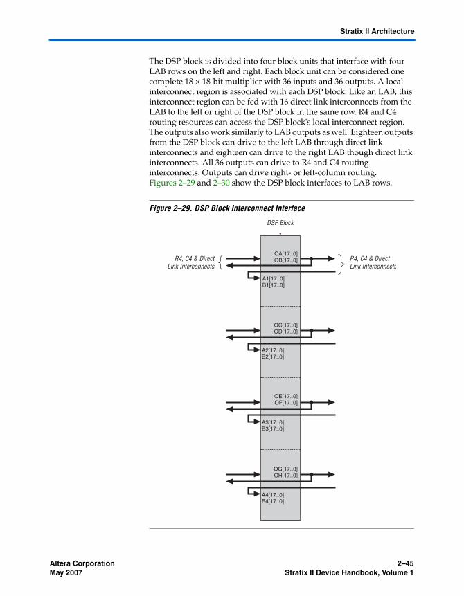
The DSP block is divided into four block units that interface with four LAB rows on the left and right. Each block unit can be considered one complete 18 × 18-bit multiplier with 36 inputs and 36 outputs. A local interconnect region is associated with each DSP block. Like an LAB, this interconnect region can be fed with 16 direct link interconnects from the LAB to the left or right of the DSP block in the same row. R4 and C4 routing resources can access the DSP block's local interconnect region. The outputs also work similarly to LAB outputs as well. Eighteen outputs from the DSP block can drive to the left LAB through direct link interconnects and eighteen can drive to the right LAB though direct link interconnects. All 36 outputs can drive to R4 and C4 routing interconnects. Outputs can drive right- or left-column routing. Figures 2–29 and 2–30 show the DSP block interfaces to LAB rows.
Figure 2–29. DSP Block Interconnect Interface
A1[17..0]B1[17..0]
A2[17..0]B2[17..0]
A3[17..0]B3[17..0]
A4[17..0]B4[17..0]
OA[17..0]OB[17..0]
OC[17..0]OD[17..0]
OE[17..0]OF[17..0]
OG[17..0]OH[17..0]
DSP Block
R4, C4 & DirectLink Interconnects
R4, C4 & DirectLink Interconnects
2–46 Altera CorporationStratix II Device Handbook, Volume 1 May 2007
Digital Signal Processing Block
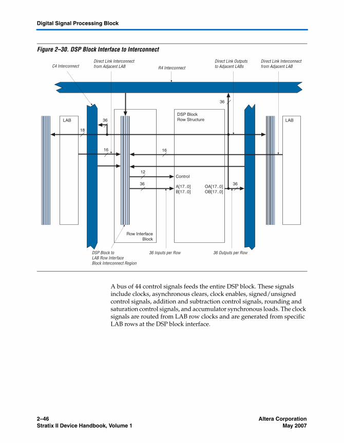
Figure 2–30. DSP Block Interface to Interconnect
A bus of 44 control signals feeds the entire DSP block. These signals include clocks, asynchronous clears, clock enables, signed/unsigned control signals, addition and subtraction control signals, rounding and saturation control signals, and accumulator synchronous loads. The clock signals are routed from LAB row clocks and are generated from specific LAB rows at the DSP block interface.
LAB LAB
Row InterfaceBlock
DSP BlockRow Structure
16
OA[17..0]OB[17..0]
A[17..0]B[17..0]
DSP Block toLAB Row InterfaceBlock Interconnect Region
36 Inputs per Row 36 Outputs per Row
R4 InterconnectC4 InterconnectDirect Link Interconnectfrom Adjacent LAB
Direct Link Outputsto Adjacent LABs
Direct Link Interconnectfrom Adjacent LAB
36
36
36
36
Control12
16
18
Altera Corporation 2–47May 2007 Stratix II Device Handbook, Volume 1
Stratix II Architecture
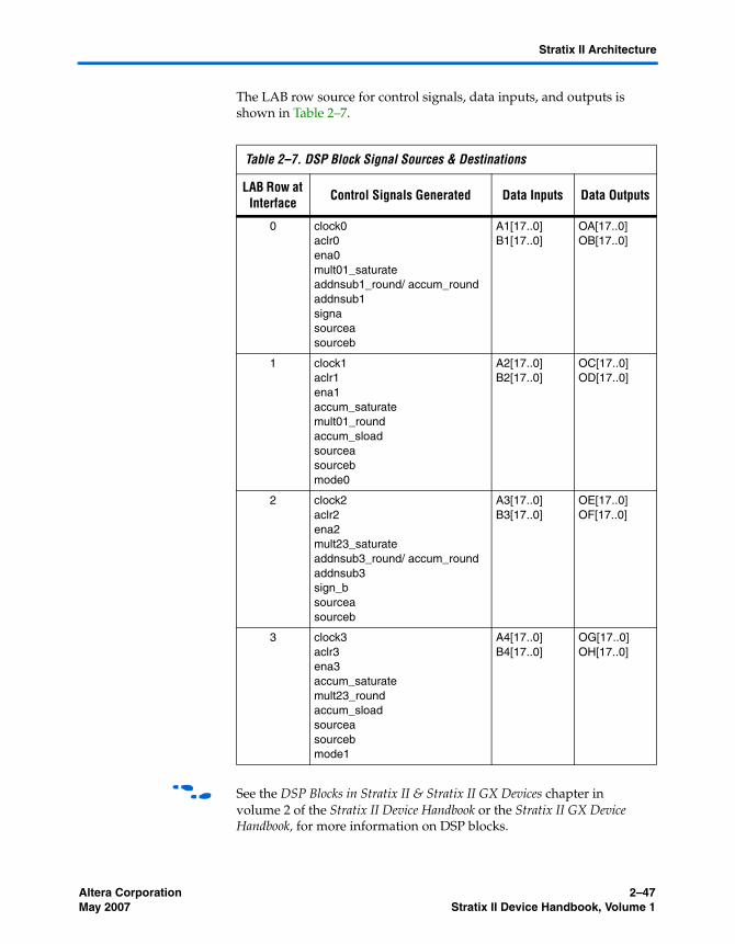
The LAB row source for control signals, data inputs, and outputs is shown in Table 2–7.
f See the DSP Blocks in Stratix II & Stratix II GX Devices chapter in volume 2 of the Stratix II Device Handbook or the Stratix II GX Device Handbook, for more information on DSP blocks.
Table 2–7. DSP Block Signal Sources & Destinations
LAB Row at Interface Control Signals Generated Data Inputs Data Outputs
0 clock0aclr0ena0mult01_saturateaddnsub1_round/ accum_roundaddnsub1signasourceasourceb
A1[17..0]B1[17..0]
OA[17..0]OB[17..0]
1 clock1aclr1ena1accum_saturatemult01_roundaccum_sloadsourceasourcebmode0
A2[17..0]B2[17..0]
OC[17..0]OD[17..0]
2 clock2aclr2ena2mult23_saturateaddnsub3_round/ accum_roundaddnsub3sign_bsourceasourceb
A3[17..0]B3[17..0]
OE[17..0]OF[17..0]
3 clock3aclr3ena3accum_saturatemult23_roundaccum_sloadsourceasourcebmode1
A4[17..0]B4[17..0]
OG[17..0]OH[17..0]
2–48 Altera CorporationStratix II Device Handbook, Volume 1 May 2007
PLLs & Clock Networks
PLLs & Clock Networks
Stratix II devices provide a hierarchical clock structure and multiple PLLs with advanced features. The large number of clocking resources in combination with the clock synthesis precision provided by enhanced and fast PLLs provides a complete clock management solution.
Global & Hierarchical Clocking
Stratix II devices provide 16 dedicated global clock networks and 32 regional clock networks (eight per device quadrant). These clocks are organized into a hierarchical clock structure that allows for up to 24 clocks per device region with low skew and delay. This hierarchical clocking scheme provides up to 48 unique clock domains in Stratix II devices.
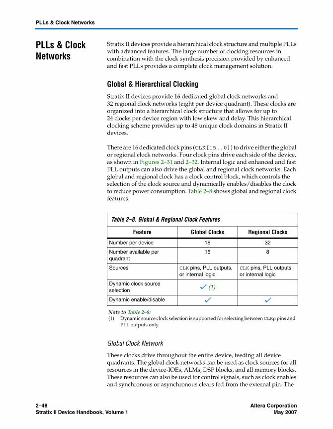
There are 16 dedicated clock pins (CLK[15..0]) to drive either the global or regional clock networks. Four clock pins drive each side of the device, as shown in Figures 2–31 and 2–32. Internal logic and enhanced and fast PLL outputs can also drive the global and regional clock networks. Each global and regional clock has a clock control block, which controls the selection of the clock source and dynamically enables/disables the clock to reduce power consumption. Table 2–8 shows global and regional clock features.
Global Clock Network
These clocks drive throughout the entire device, feeding all device quadrants. The global clock networks can be used as clock sources for all resources in the device-IOEs, ALMs, DSP blocks, and all memory blocks. These resources can also be used for control signals, such as clock enables and synchronous or asynchronous clears fed from the external pin. The
Table 2–8. Global & Regional Clock Features
Feature Global Clocks Regional Clocks
Number per device 16 32
Number available per quadrant
16 8
Sources CLK pins, PLL outputs, or internal logic
CLK pins, PLL outputs, or internal logic
Dynamic clock source selection v (1)
Dynamic enable/disable v v
Note to Table 2–8:(1) Dynamic source clock selection is supported for selecting between CLKp pins and
PLL outputs only.
Altera Corporation 2–49May 2007 Stratix II Device Handbook, Volume 1
Stratix II Architecture
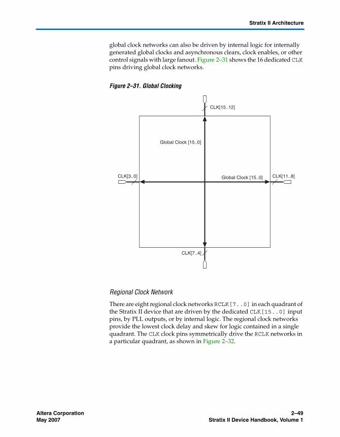
global clock networks can also be driven by internal logic for internally generated global clocks and asynchronous clears, clock enables, or other control signals with large fanout. Figure 2–31 shows the 16 dedicated CLK pins driving global clock networks.
Figure 2–31. Global Clocking
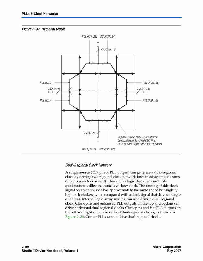
Regional Clock Network
There are eight regional clock networks RCLK[7..0] in each quadrant of the Stratix II device that are driven by the dedicated CLK[15..0] input pins, by PLL outputs, or by internal logic. The regional clock networks provide the lowest clock delay and skew for logic contained in a single quadrant. The CLK clock pins symmetrically drive the RCLK networks in a particular quadrant, as shown in Figure 2–32.
Global Clock [15..0]
CLK[15..12]
CLK[3..0]
CLK[7..4]
CLK[11..8] Global Clock [15..0]
2–50 Altera CorporationStratix II Device Handbook, Volume 1 May 2007
PLLs & Clock Networks
Figure 2–32. Regional Clocks
Dual-Regional Clock Network
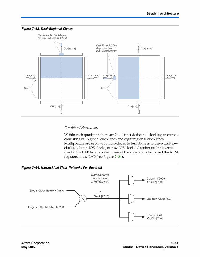
A single source (CLK pin or PLL output) can generate a dual-regional clock by driving two regional clock network lines in adjacent quadrants (one from each quadrant). This allows logic that spans multiple quadrants to utilize the same low skew clock. The routing of this clock signal on an entire side has approximately the same speed but slightly higher clock skew when compared with a clock signal that drives a single quadrant. Internal logic-array routing can also drive a dual-regional clock. Clock pins and enhanced PLL outputs on the top and bottom can drive horizontal dual-regional clocks. Clock pins and fast PLL outputs on the left and right can drive vertical dual-regional clocks, as shown in Figure 2–33. Corner PLLs cannot drive dual-regional clocks.
RCLK[3..0]
RCLK[7..4]
RCLK[11..8] RCLK[15..12]
RCLK[31..28] RCLK[27..24]
RCLK[19..16]
RCLK[23..20]
CLK[15..12]
CLK[3..0]
CLK[7..4]
CLK[11..8]
Regional Clocks Only Drive a Device Quadrant from Specified CLK Pins, PLLs or Core Logic within that Quadrant
Altera Corporation 2–51May 2007 Stratix II Device Handbook, Volume 1
Stratix II Architecture
Figure 2–33. Dual-Regional Clocks
Combined Resources
Within each quadrant, there are 24 distinct dedicated clocking resources consisting of 16 global clock lines and eight regional clock lines. Multiplexers are used with these clocks to form busses to drive LAB row clocks, column IOE clocks, or row IOE clocks. Another multiplexer is used at the LAB level to select three of the six row clocks to feed the ALM registers in the LAB (see Figure 2–34).
Figure 2–34. Hierarchical Clock Networks Per Quadrant
Clock Pins or PLL Clock OutputsCan Drive Dual-Regional Network
CLK[15..12]
CLK[11..8]
CLK[7..4]
CLK[3..0]
PLLsPLLs
Clock Pins or PLL ClockOutputs Can DriveDual-Regional Network
CLK[15..12]
CLK[11..8]
CLK[7..4]
CLK[3..0]
Clock [23..0]
Column I/O CellIO_CLK[7..0]
Lab Row Clock [5..0]
Row I/O CellIO_CLK[7..0]
Global Clock Network [15..0]
Regional Clock Network [7..0]
Clocks Availableto a Quadrant
or Half-Quadrant
2–52 Altera CorporationStratix II Device Handbook, Volume 1 May 2007
PLLs & Clock Networks
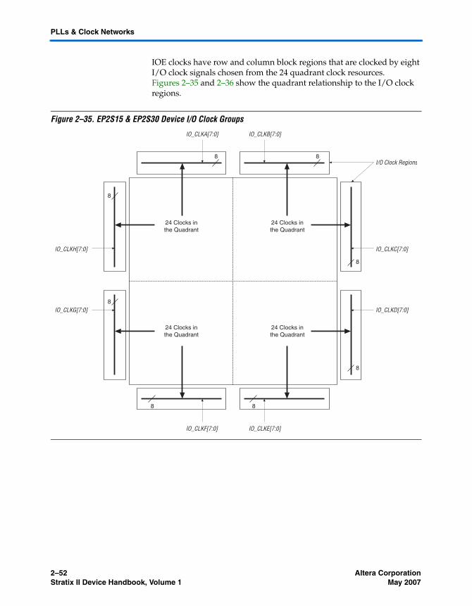
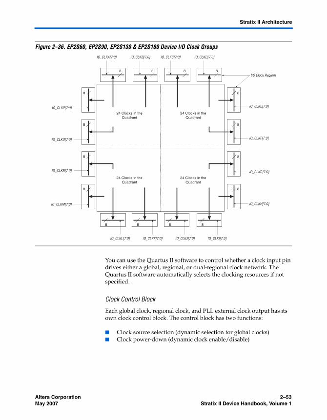
IOE clocks have row and column block regions that are clocked by eight I/O clock signals chosen from the 24 quadrant clock resources. Figures 2–35 and 2–36 show the quadrant relationship to the I/O clock regions.
Figure 2–35. EP2S15 & EP2S30 Device I/O Clock Groups
IO_CLKC[7:0]
IO_CLKF[7:0] IO_CLKE[7:0]
IO_CLKA[7:0] IO_CLKB[7:0]
IO_CLKD[7:0]
IO_CLKH[7:0]
IO_CLKG[7:0]
8
8
24 Clocks inthe Quadrant
24 Clocks inthe Quadrant
24 Clocks inthe Quadrant
24 Clocks inthe Quadrant
8
8
8
8
8 8I/O Clock Regions
Altera Corporation 2–53May 2007 Stratix II Device Handbook, Volume 1
Stratix II Architecture
Figure 2–36. EP2S60, EP2S90, EP2S130 & EP2S180 Device I/O Clock Groups
You can use the Quartus II software to control whether a clock input pin drives either a global, regional, or dual-regional clock network. The Quartus II software automatically selects the clocking resources if not specified.
Clock Control Block
Each global clock, regional clock, and PLL external clock output has its own clock control block. The control block has two functions:
■ Clock source selection (dynamic selection for global clocks)■ Clock power-down (dynamic clock enable/disable)
IO_CLKJ[7:0] IO_CLKI[7:0]
IO_CLKA[7:0] IO_CLKB[7:0]
8
24 Clocks in theQuadrant
24 Clocks in theQuadrant
24 Clocks in theQuadrant
24 Clocks in theQuadrant
8 8 8
I/O Clock Regions
IO_CLKL[7:0] IO_CLKK[7:0]
IO_CLKC[7:0] IO_CLKD[7:0]
8 8 8 8
8
8
8
8
8
8
8
8
IO_CLKE[7:0]
IO_CLKF[7:0]
IO_CLKG[7:0]
IO_CLKH[7:0]
IO_CLKN[7:0]
IO_CLKM[7:0]
IO_CLKP[7:0]
IO_CLKO[7:0]
2–54 Altera CorporationStratix II Device Handbook, Volume 1 May 2007
PLLs & Clock Networks
1 When using the global or regional clock control blocks in Stratix II devices to select between multiple clocks or to enable and disable clock networks, be aware of possible narrow pulses or glitches when switching from one clock signal to another. A glitch or runt pulse has a width that is less than the width of the highest frequency input clock signal. To prevent logic errors within the FPGA, Altera recommends that you build circuits that filter out glitches and runt pulses.
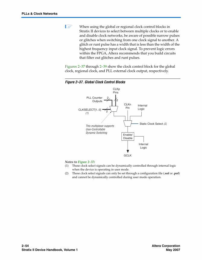
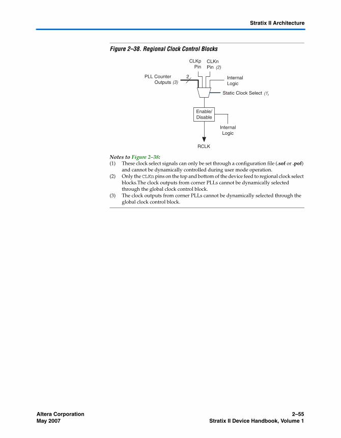
Figures 2–37 through 2–39 show the clock control block for the global clock, regional clock, and PLL external clock output, respectively.
Figure 2–37. Global Clock Control Blocks
Notes to Figure 2–37:(1) These clock select signals can be dynamically controlled through internal logic
when the device is operating in user mode.(2) These clock select signals can only be set through a configuration file (.sof or .pof)
and cannot be dynamically controlled during user mode operation.
CLKpPins
PLL CounterOutputs
InternalLogic
CLKnPin
Enable/Disable
GCLK
InternalLogic
Static Clock SelectThis multiplexer supportsUser-ControllableDynamic Switching
CLKSELECT[1..0](1)
(2)
2
22
Altera Corporation 2–55May 2007 Stratix II Device Handbook, Volume 1
Stratix II Architecture
Figure 2–38. Regional Clock Control Blocks
Notes to Figure 2–38:(1) These clock select signals can only be set through a configuration file (.sof or .pof)
and cannot be dynamically controlled during user mode operation.(2) Only the CLKn pins on the top and bottom of the device feed to regional clock select
blocks.The clock outputs from corner PLLs cannot be dynamically selected through the global clock control block.
(3) The clock outputs from corner PLLs cannot be dynamically selected through the global clock control block.
CLKpPin
PLL CounterOutputs
InternalLogic
CLKnPin
Enable/Disable
RCLK
InternalLogic
Static Clock Select (1)
2
(2)
(3)
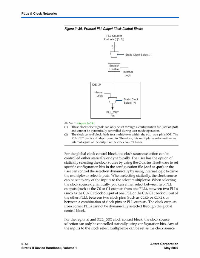
2–56 Altera CorporationStratix II Device Handbook, Volume 1 May 2007
PLLs & Clock Networks
Figure 2–39. External PLL Output Clock Control Blocks
Notes to Figure 2–39:(1) These clock select signals can only be set through a configuration file (.sof or .pof)
and cannot be dynamically controlled during user mode operation.(2) The clock control block feeds to a multiplexer within the PLL_OUT pin’s IOE. The
PLL_OUT pin is a dual-purpose pin. Therefore, this multiplexer selects either an internal signal or the output of the clock control block.
For the global clock control block, the clock source selection can be controlled either statically or dynamically. The user has the option of statically selecting the clock source by using the Quartus II software to set specific configuration bits in the configuration file (.sof or .pof) or the user can control the selection dynamically by using internal logic to drive the multiplexor select inputs. When selecting statically, the clock source can be set to any of the inputs to the select multiplexor. When selecting the clock source dynamically, you can either select between two PLL outputs (such as the C0 or C1 outputs from one PLL), between two PLLs (such as the C0/C1 clock output of one PLL or the C0/C1 c1ock output of the other PLL), between two clock pins (such as CLK0 or CLK1), or between a combination of clock pins or PLL outputs. The clock outputs from corner PLLs cannot be dynamically selected through the global control block.
For the regional and PLL_OUT clock control block, the clock source selection can only be controlled statically using configuration bits. Any of the inputs to the clock select multiplexor can be set as the clock source.
PLL CounterOutputs (c[5..0])
Enable/Disable
PLL_OUTPin
InternalLogic
Static Clock Select
IOE
(1)
Static ClockSelect (1)
6
InternalLogic
(2)
Altera Corporation 2–57May 2007 Stratix II Device Handbook, Volume 1
Stratix II Architecture
The Stratix II clock networks can be disabled (powered down) by both static and dynamic approaches. When a clock net is powered down, all the logic fed by the clock net is in an off-state thereby reducing the overall power consumption of the device.
The global and regional clock networks can be powered down statically through a setting in the configuration (.sof or .pof) file. Clock networks that are not used are automatically powered down through configuration bit settings in the configuration file generated by the Quartus II software.
The dynamic clock enable/disable feature allows the internal logic to control power up/down synchronously on GCLK and RCLK nets and PLL_OUT pins. This function is independent of the PLL and is applied directly on the clock network or PLL_OUT pin, as shown in Figures 2–37 through 2–39.
1 The following restrictions for the input clock pins apply:
• CLK0 pin -> inclk[0] of CLKCTRL• CLK1 pin -> inclk[1] of CLKCTRL• CLK2 pin -> inclk[0] of CLKCTRL• CLK3 pin -> inclk[1] of CLKCTRL
In general, even CLK numbers connect to the inclk[0] port of CLKCTRL, and odd CLK numbers connect to the inclk[1] port of CLKCTRL.
Failure to comply with these restrictions will result in a no-fit error.
Enhanced & Fast PLLs
Stratix II devices provide robust clock management and synthesis using up to four enhanced PLLs and eight fast PLLs. These PLLs increase performance and provide advanced clock interfacing and clock-frequency synthesis. With features such as clock switchover, spread-spectrum clocking, reconfigurable bandwidth, phase control, and reconfigurable phase shifting, the Stratix II device’s enhanced PLLs provide you with complete control of clocks and system timing. The fast PLLs provide general purpose clocking with multiplication and phase shifting as well as high-speed outputs for high-speed differential I/O support. Enhanced and fast PLLs work together with the Stratix II high-speed I/O and advanced clock architecture to provide significant improvements in system performance and bandwidth.
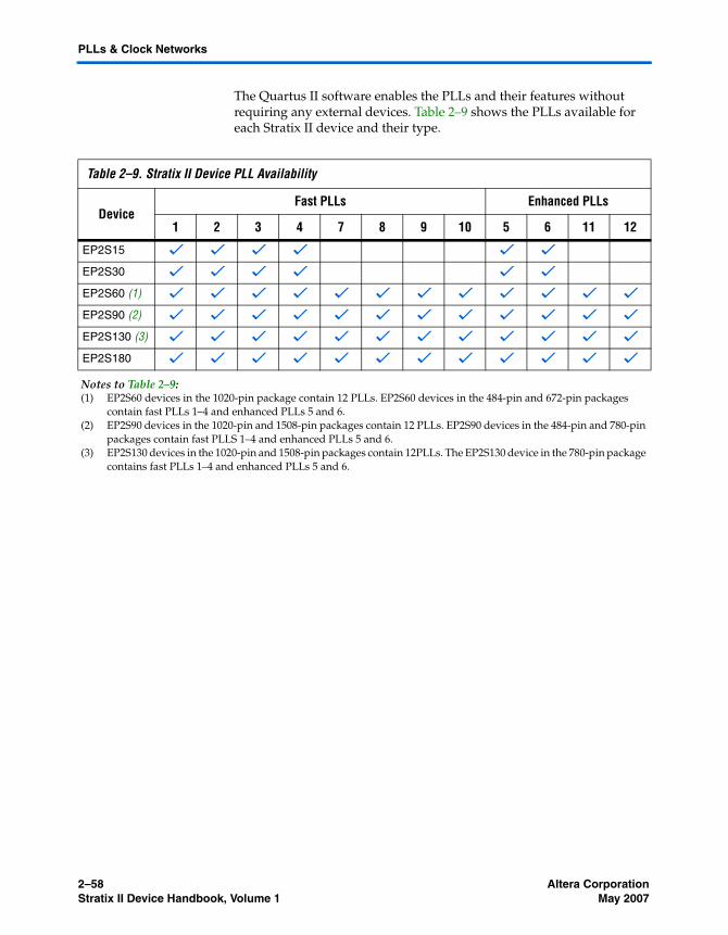
2–58 Altera CorporationStratix II Device Handbook, Volume 1 May 2007
PLLs & Clock Networks
The Quartus II software enables the PLLs and their features without requiring any external devices. Table 2–9 shows the PLLs available for each Stratix II device and their type.
Table 2–9. Stratix II Device PLL Availability
DeviceFast PLLs Enhanced PLLs
1 2 3 4 7 8 9 10 5 6 11 12
EP2S15 v v v v v v
EP2S30 v v v v v v
EP2S60 (1) v v v v v v v v v v v v
EP2S90 (2) v v v v v v v v v v v v
EP2S130 (3) v v v v v v v v v v v v
EP2S180 v v v v v v v v v v v v
Notes to Table 2–9:(1) EP2S60 devices in the 1020-pin package contain 12 PLLs. EP2S60 devices in the 484-pin and 672-pin packages
contain fast PLLs 1–4 and enhanced PLLs 5 and 6.(2) EP2S90 devices in the 1020-pin and 1508-pin packages contain 12 PLLs. EP2S90 devices in the 484-pin and 780-pin
packages contain fast PLLS 1–4 and enhanced PLLs 5 and 6.(3) EP2S130 devices in the 1020-pin and 1508-pin packages contain 12PLLs. The EP2S130 device in the 780-pin package
contains fast PLLs 1–4 and enhanced PLLs 5 and 6.
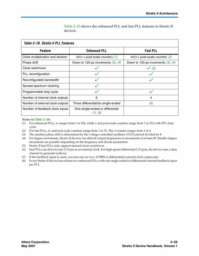
Altera Corporation 2–59May 2007 Stratix II Device Handbook, Volume 1
Stratix II Architecture
Table 2–10 shows the enhanced PLL and fast PLL features in Stratix II devices.
Table 2–10. Stratix II PLL Features
Feature Enhanced PLL Fast PLL
Clock multiplication and division m/(n × post-scale counter) (1) m/(n × post-scale counter) (2)
Phase shift Down to 125-ps increments (3), (4) Down to 125-ps increments (3), (4)
Clock switchover v v (5)
PLL reconfiguration v v
Reconfigurable bandwidth v v
Spread spectrum clocking v
Programmable duty cycle v v
Number of internal clock outputs 6 4
Number of external clock outputs Three differential/six single-ended (6)
Number of feedback clock inputs One single-ended or differential(7), (8)
Notes to Table 2–10:(1) For enhanced PLLs, m ranges from 1 to 256, while n and post-scale counters range from 1 to 512 with 50% duty
cycle.(2) For fast PLLs, m, and post-scale counters range from 1 to 32. The n counter ranges from 1 to 4.(3) The smallest phase shift is determined by the voltage controlled oscillator (VCO) period divided by 8.(4) For degree increments, Stratix II devices can shift all output frequencies in increments of at least 45. Smaller degree
increments are possible depending on the frequency and divide parameters.(5) Stratix II fast PLLs only support manual clock switchover.(6) Fast PLLs can drive to any I/O pin as an external clock. For high-speed differential I/O pins, the device uses a data
channel to generate txclkout.(7) If the feedback input is used, you lose one (or two, if FBIN is differential) external clock output pin.(8) Every Stratix II device has at least two enhanced PLLs with one single-ended or differential external feedback input
per PLL.

2–60 Altera CorporationStratix II Device Handbook, Volume 1 May 2007
PLLs & Clock Networks
Figure 2–40 shows a top-level diagram of the Stratix II device and PLL floorplan.
Figure 2–40. PLL Locations
Figures 2–41 and 2–42 shows the global and regional clocking from the fast PLL outputs and the side clock pins.
FPLL7CLK FPLL10CLK
FPLL9CLK
CLK[8..11]
FPLL8CLK
CLK[3..0]
7
1
2
8
10
4
3
9
511
612
CLK[7..4]
CLK[15..12]
PLLs
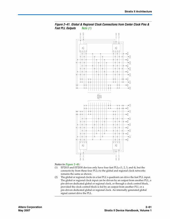
Altera Corporation 2–61May 2007 Stratix II Device Handbook, Volume 1
Stratix II Architecture
Figure 2–41. Global & Regional Clock Connections from Center Clock Pins & Fast PLL Outputs Note (1)
Notes to Figure 2–41:(1) EP2S15 and EP2S30 devices only have four fast PLLs (1, 2, 3, and 4), but the
connectivity from these four PLLs to the global and regional clock networks remains the same as shown.
(2) The global or regional clocks in a fast PLL's quadrant can drive the fast PLL input. The global or regional clock input can be driven by an output from another PLL, a pin-driven dedicated global or regional clock, or through a clock control block, provided the clock control block is fed by an output from another PLL or a pin-driven dedicated global or regional clock. An internally generated global signal cannot drive the PLL.
C0
C1
C2
C3
Fast
PLL
1
RC
K0
RC
K2
RC
K1
RC
K3
GC
K0
GC
K2
GC
K9
GC
K11
GC
K1
GC
K3
GC
K8
GC
K10
RC
K4
RC
K6
RC
K5
RC
K7
RC
K17
RC
K16
RC
K18
RC
K19
RC
K21
RC
K23
RC
K20
RC
K22
C0
C1
C2
C3
Fast
PLL
2
Logi
c Ar
ray
Sign
al In
put
To C
lock
Netw
ork
CLK
0
CLK
1
CLK
2
CLK
3
C0
C1
C2
C3
Fast
PLL
4
C0
C1
C2
C3
Fast
PLL
3
CLK
11
CLK
10
CLK
9
CLK
8
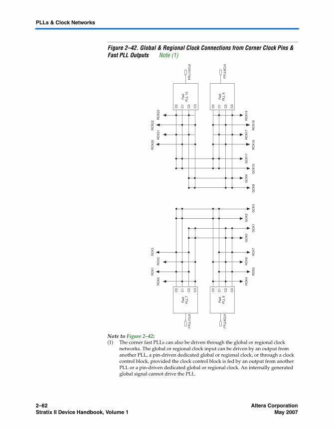
2–62 Altera CorporationStratix II Device Handbook, Volume 1 May 2007
PLLs & Clock Networks
Figure 2–42. Global & Regional Clock Connections from Corner Clock Pins & Fast PLL Outputs Note (1)
Note to Figure 2–42:(1) The corner fast PLLs can also be driven through the global or regional clock
networks. The global or regional clock input can be driven by an output from another PLL, a pin-driven dedicated global or regional clock, or through a clock control block, provided the clock control block is fed by an output from another PLL or a pin-driven dedicated global or regional clock. An internally generated global signal cannot drive the PLL.
C0
C1
C2
C3
Fast
PLL
7
RC
K0
RC
K2
RC
K1
RC
K3
GC
K0
GC
K2
GC
K9
GC
K11
GC
K1
GC
K3
GC
K8
GC
K10
RC
K4
RC
K6
RC
K5
RC
K7
RC
K17
RC
K16
RC
K18
RC
K19
RC
K21
RC
K23
RC
K20
RC
K22
C0
C1
C2
C3
Fast
PLL
8
C0
C1
C2
C3
Fast
PLL
10
C0
C1
C2
C3
Fast
PLL
9
FP
LL7C
LK
FP
LL8C
LK
FP
LL10
CLK
FP
LL9C
LK
Altera Corporation 2–63May 2007 Stratix II Device Handbook, Volume 1
Stratix II Architecture
Figure 2–43 shows the global and regional clocking from enhanced PLL outputs and top and bottom CLK pins. The connections to the global and regional clocks from the top clock pins and enhanced PLL outputs is shown in Table 2–11. The connections to the clocks from the bottom clock pins is shown in Table 2–12.
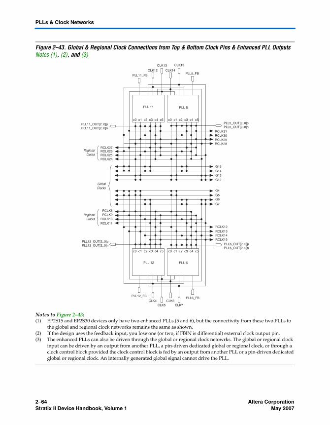
2–64 Altera CorporationStratix II Device Handbook, Volume 1 May 2007
PLLs & Clock Networks
Figure 2–43. Global & Regional Clock Connections from Top & Bottom Clock Pins & Enhanced PLL Outputs Notes (1), (2), and (3)
Notes to Figure 2–43:(1) EP2S15 and EP2S30 devices only have two enhanced PLLs (5 and 6), but the connectivity from these two PLLs to
the global and regional clock networks remains the same as shown.(2) If the design uses the feedback input, you lose one (or two, if FBIN is differential) external clock output pin.(3) The enhanced PLLs can also be driven through the global or regional clock netowrks. The global or regional clock
input can be driven by an output from another PLL, a pin-driven dedicated global or regional clock, or through a clock control block provided the clock control block is fed by an output from another PLL or a pin-driven dedicated global or regional clock. An internally generated global signal cannot drive the PLL.
G15G14G13G12
RCLK31RCLK30RCLK29RCLK28
RCLK27RCLK26RCLK25RCLK24
G7
G6G5G4
RCLK15RCLK14RCLK13RCLK12
RCLK11RCLK10
RCLK9RCLK8
PLL 6
CLK7CLK6
CLK5CLK4
PLL 12
PLL 5
c0 c1 c2 c3 c4 c5 c0 c1 c2 c3 c4 c5
c0 c1 c2 c3 c4 c5 c0 c1 c2 c3 c4 c5
CLK14
CLK15CLK13
CLK12
PLL 11
PLL11_FB
PLL5_OUT[2..0]pPLL5_OUT[2..0]n
PLL11_OUT[2..0]pPLL11_OUT[2..0]n
PLL12_OUT[2..0]pPLL12_OUT[2..0]n PLL6_OUT[2..0]p
PLL6_OUT[2..0]n
PLL5_FB
PLL12_FBPLL6_FB
GlobalClocks
RegionalClocks
RegionalClocks
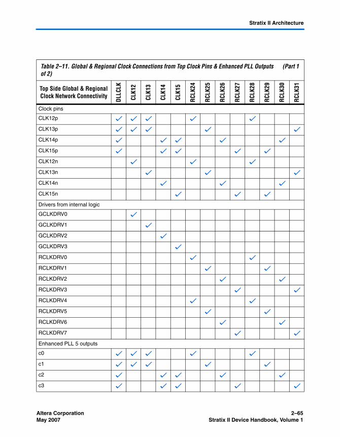
Altera Corporation 2–65May 2007 Stratix II Device Handbook, Volume 1
Stratix II Architecture
Table 2–11. Global & Regional Clock Connections from Top Clock Pins & Enhanced PLL Outputs (Part 1 of 2)
Top Side Global & Regional Clock Network Connectivity
DLLC
LK
CLK1
2
CLK1
3
CLK1
4
CLK1
5
RCLK
24
RCLK
25
RCLK
26
RCLK
27
RCLK
28
RCLK
29
RCLK
30
RCLK
31
Clock pins
CLK12p v v v v v
CLK13p v v v v v
CLK14p v v v v v
CLK15p v v v v v
CLK12n v v v
CLK13n v v v
CLK14n v v v
CLK15n v v v
Drivers from internal logic
GCLKDRV0 v
GCLKDRV1 v
GCLKDRV2 v
GCLKDRV3 v
RCLKDRV0 v v
RCLKDRV1 v v
RCLKDRV2 v v
RCLKDRV3 v v
RCLKDRV4 v v
RCLKDRV5 v v
RCLKDRV6 v v
RCLKDRV7 v v
Enhanced PLL 5 outputs
c0 v v v v v
c1 v v v v v
c2 v v v v v
c3 v v v v v
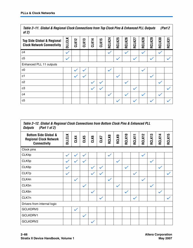
2–66 Altera CorporationStratix II Device Handbook, Volume 1 May 2007
PLLs & Clock Networks
c4 v v v v v
c5 v v v v v
Enhanced PLL 11 outputs
c0 v v v v
c1 v v v v
c2 v v v v
c3 v v v v
c4 v v v v
c5 v v v v
Table 2–11. Global & Regional Clock Connections from Top Clock Pins & Enhanced PLL Outputs (Part 2 of 2)
Top Side Global & Regional Clock Network Connectivity
DLLC
LK
CLK1
2
CLK1
3
CLK1
4
CLK1
5
RCLK
24
RCLK
25
RCLK
26
RCLK
27
RCLK
28
RCLK
29
RCLK
30
RCLK
31
Table 2–12. Global & Regional Clock Connections from Bottom Clock Pins & Enhanced PLL Outputs (Part 1 of 2)
Bottom Side Global & Regional Clock Network
Connectivity DLLC
LK
CLK4
CLK5
CLK6
CLK7
RCLK
8
RCLK
9
RCLK
10
RCLK
11
RCLK
12
RCLK
13
RCLK
14
RCLK
15
Clock pins
CLK4p v v v v v
CLK5p v v v v v
CLK6p v v v v v
CLK7p v v v v v
CLK4n v v v
CLK5n v v v
CLK6n v v v
CLK7n v v v
Drivers from internal logic
GCLKDRV0 v
GCLKDRV1 v
GCLKDRV2 v
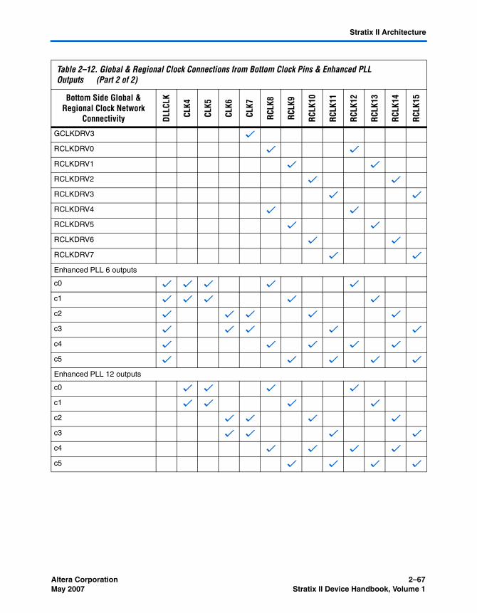
Altera Corporation 2–67May 2007 Stratix II Device Handbook, Volume 1
Stratix II Architecture
GCLKDRV3 v
RCLKDRV0 v v
RCLKDRV1 v v
RCLKDRV2 v v
RCLKDRV3 v v
RCLKDRV4 v v
RCLKDRV5 v v
RCLKDRV6 v v
RCLKDRV7 v v
Enhanced PLL 6 outputs
c0 v v v v v
c1 v v v v v
c2 v v v v v
c3 v v v v v
c4 v v v v v
c5 v v v v v
Enhanced PLL 12 outputs
c0 v v v v
c1 v v v v
c2 v v v v
c3 v v v v
c4 v v v v
c5 v v v v
Table 2–12. Global & Regional Clock Connections from Bottom Clock Pins & Enhanced PLL Outputs (Part 2 of 2)
Bottom Side Global & Regional Clock Network
Connectivity DLLC
LK
CLK4
CLK5
CLK6
CLK7
RCLK
8
RCLK
9
RCLK
10
RCLK
11
RCLK
12
RCLK
13
RCLK
14
RCLK
15
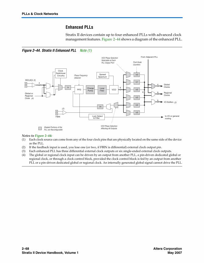
2–68 Altera CorporationStratix II Device Handbook, Volume 1 May 2007
PLLs & Clock Networks
Enhanced PLLs
Stratix II devices contain up to four enhanced PLLs with advanced clock management features. Figure 2–44 shows a diagram of the enhanced PLL.
Figure 2–44. Stratix II Enhanced PLL Note (1)
Notes to Figure 2–44:(1) Each clock source can come from any of the four clock pins that are physically located on the same side of the device
as the PLL.(2) If the feedback input is used, you lose one (or two, if FBIN is differential) external clock output pin.(3) Each enhanced PLL has three differential external clock outputs or six single-ended external clock outputs.(4) The global or regional clock input can be driven by an output from another PLL, a pin-driven dedicated global or
regional clock, or through a clock control block, provided the clock control block is fed by an output from another PLL or a pin-driven dedicated global or regional clock. An internally generated global signal cannot drive the PLL.
/n ChargePump VCO /c2
/c3
/c4
/c0
8
4
6
4 GlobalClocks
/c1
Lock Detect to I/O or generalrouting
INCLK[3..0]
FBIN
Global or RegionalClock
PFD
/c5
From Adjacent PLL
/m
SpreadSpectrum
I/O Buffers (3)
(2)
LoopFilter
& Filter
Post-ScaleCounters
ClockSwitchover
Circuitry Phase FrequencyDetector
VCO Phase SelectionSelectable at EachPLL Output Port
VCO Phase SelectionAffecting All OutputsShaded Portions of the
PLL are Reconfigurable
RegionalClocks
8
6(4)
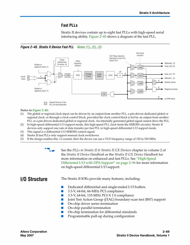
Altera Corporation 2–69May 2007 Stratix II Device Handbook, Volume 1
Stratix II Architecture
Fast PLLs
Stratix II devices contain up to eight fast PLLs with high-speed serial interfacing ability. Figure 2–45 shows a diagram of the fast PLL.
Figure 2–45. Stratix II Device Fast PLL Notes (1), (2), (3)
Notes to Figure 2–45:(1) The global or regional clock input can be driven by an output from another PLL, a pin-driven dedicated global or
regional clock, or through a clock control block, provided the clock control block is fed by an output from another PLL or a pin-driven dedicated global or regional clock. An internally generated global signal cannot drive the PLL.
(2) In high-speed differential I/O support mode, this high-speed PLL clock feeds the SERDES circuitry. Stratix II devices only support one rate of data transfer per fast PLL in high-speed differential I/O support mode.
(3) This signal is a differential I/O SERDES control signal.(4) Stratix II fast PLLs only support manual clock switchover.(5) If the design enables this ÷2 counter, then the device can use a VCO frequency range of 150 to 520 MHz.
f See the PLLs in Stratix II & Stratix II GX Devices chapter in volume 2 of the Stratix II Device Handbook or the Stratix II GX Device Handbook for more information on enhanced and fast PLLs. See “High-Speed Differential I/O with DPA Support” on page 2–96 for more information on high-speed differential I/O support.
I/O Structure The Stratix II IOEs provide many features, including:
■ Dedicated differential and single-ended I/O buffers■ 3.3-V, 64-bit, 66-MHz PCI compliance■ 3.3-V, 64-bit, 133-MHz PCI-X 1.0 compliance■ Joint Test Action Group (JTAG) boundary-scan test (BST) support■ On-chip driver series termination■ On-chip parallel termination■ On-chip termination for differential standards■ Programmable pull-up during configuration
ChargePump VCO ÷c1
8
8
4
4
8
ClockInput
PFD
÷c0
÷m
LoopFilter
PhaseFrequencyDetector
VCO Phase SelectionSelectable at each PLLOutput Port
Post-ScaleCounters
Global clocks
diffioclk1
load_en1
load_en0
diffioclk0
Regional clocks
to DPA block
Global orregional clock (1)
Global orregional clock (1)
÷c2
÷k
÷c3
÷n4
ClockSwitchoverCircuitry (4)
Shaded Portions of thePLL are Reconfigurable
(2)
(2)
(3)
(3)
(5)
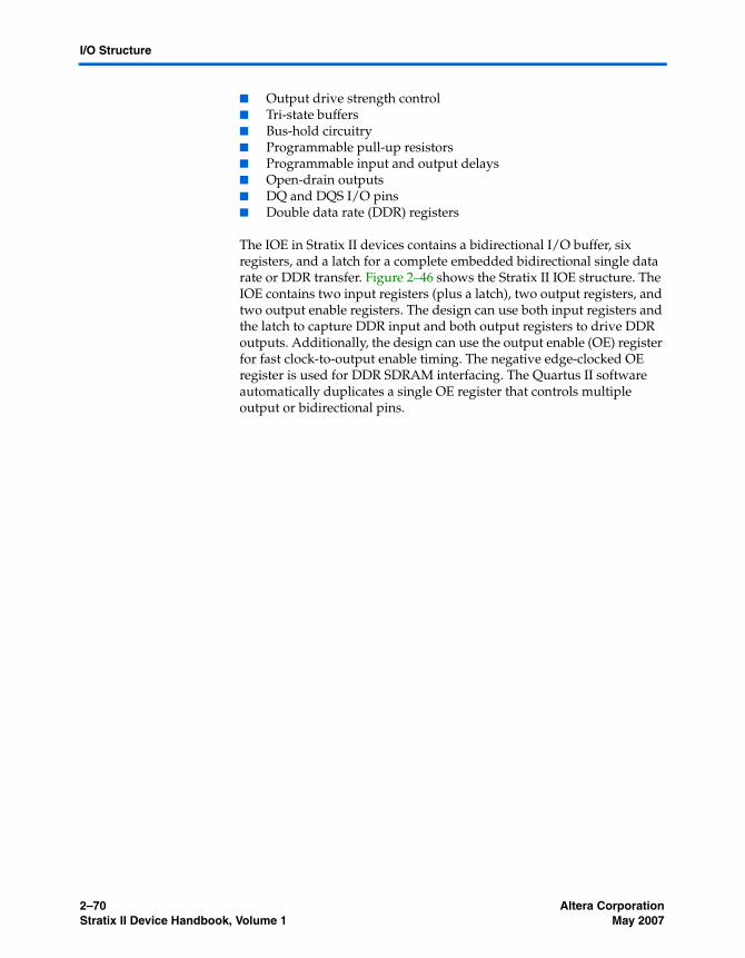
2–70 Altera CorporationStratix II Device Handbook, Volume 1 May 2007
I/O Structure
■ Output drive strength control■ Tri-state buffers■ Bus-hold circuitry■ Programmable pull-up resistors■ Programmable input and output delays■ Open-drain outputs■ DQ and DQS I/O pins■ Double data rate (DDR) registers
The IOE in Stratix II devices contains a bidirectional I/O buffer, six registers, and a latch for a complete embedded bidirectional single data rate or DDR transfer. Figure 2–46 shows the Stratix II IOE structure. The IOE contains two input registers (plus a latch), two output registers, and two output enable registers. The design can use both input registers and the latch to capture DDR input and both output registers to drive DDR outputs. Additionally, the design can use the output enable (OE) register for fast clock-to-output enable timing. The negative edge-clocked OE register is used for DDR SDRAM interfacing. The Quartus II software automatically duplicates a single OE register that controls multiple output or bidirectional pins.
Altera Corporation 2–71May 2007 Stratix II Device Handbook, Volume 1
Stratix II Architecture
Figure 2–46. Stratix II IOE Structure
The IOEs are located in I/O blocks around the periphery of the Stratix II device. There are up to four IOEs per row I/O block and four IOEs per column I/O block. The row I/O blocks drive row, column, or direct link interconnects. The column I/O blocks drive column interconnects. Figure 2–47 shows how a row I/O block connects to the logic array. Figure 2–48 shows how a column I/O block connects to the logic array.
D Q
Output Register
Output A
D Q
Output Register
Output B
Input A
Input B
D Q
OE Register
OE
D Q
OE Register
D Q
Input Register
D Q
Input Register
D Q
Input Latch
Logic Array
CLK
ENA
2–72 Altera CorporationStratix II Device Handbook, Volume 1 May 2007
I/O Structure
Figure 2–47. Row I/O Block Connection to the Interconnect Note (1)
Note to Figure 2–47:(1) The 32 data and control signals consist of eight data out lines: four lines each for DDR applications
io_dataouta[3..0] and io_dataoutb[3..0], four output enables io_oe[3..0], four input clock enables io_ce_in[3..0], four output clock enables io_ce_out[3..0], four clocks io_clk[3..0], four asynchronous clear and preset signals io_aclr/apreset[3..0], and four synchronous clear and preset signals io_sclr/spreset[3..0].
32
R4 & R24Interconnects C4 Interconnect
I/O Block Local Interconnect
32 Data & Control Signals from Logic Array (1)
io_dataina[3..0]io_datainb[3..0]
io_clk[7:0]
Horizontal I/OBlock Containsup to Four IOEs
Direct LinkInterconnect
to Adjacent LAB
Direct LinkInterconnect
to Adjacent LAB
LAB LocalInterconnect
LAB HorizontalI/O Block
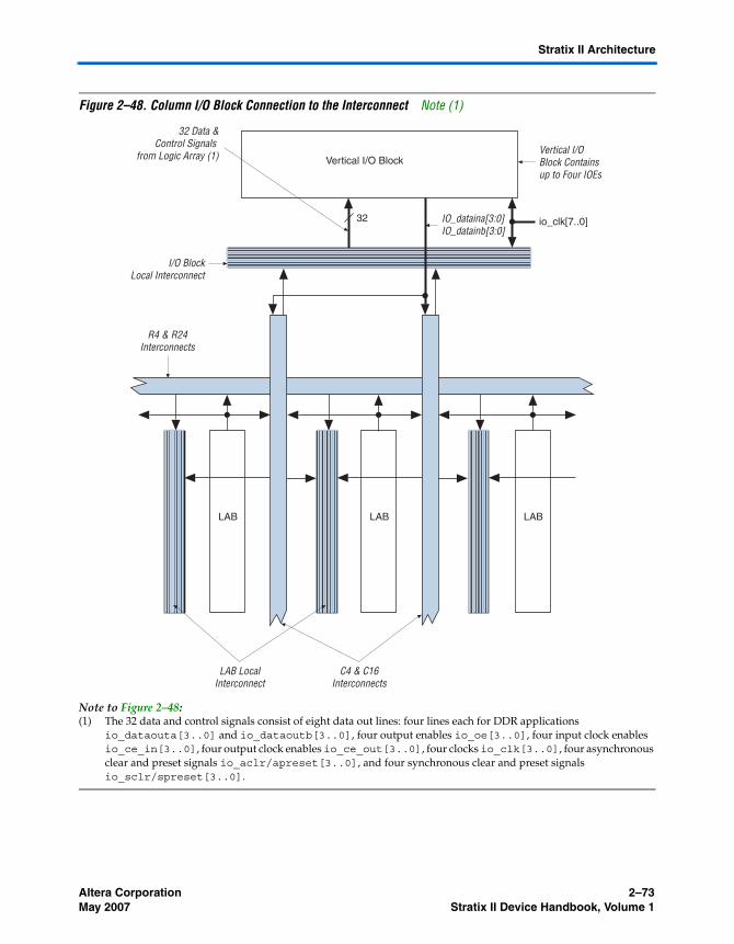
Altera Corporation 2–73May 2007 Stratix II Device Handbook, Volume 1
Stratix II Architecture
Figure 2–48. Column I/O Block Connection to the Interconnect Note (1)
Note to Figure 2–48:(1) The 32 data and control signals consist of eight data out lines: four lines each for DDR applications
io_dataouta[3..0] and io_dataoutb[3..0], four output enables io_oe[3..0], four input clock enables io_ce_in[3..0], four output clock enables io_ce_out[3..0], four clocks io_clk[3..0], four asynchronous clear and preset signals io_aclr/apreset[3..0], and four synchronous clear and preset signals io_sclr/spreset[3..0].
32 Data &Control Signals
from Logic Array (1) Vertical I/O Block Containsup to Four IOEs
I/O BlockLocal Interconnect
IO_dataina[3:0]IO_datainb[3:0]
R4 & R24Interconnects
LAB LocalInterconnect
C4 & C16Interconnects
32
LAB LAB LAB
io_clk[7..0]
Vertical I/O Block
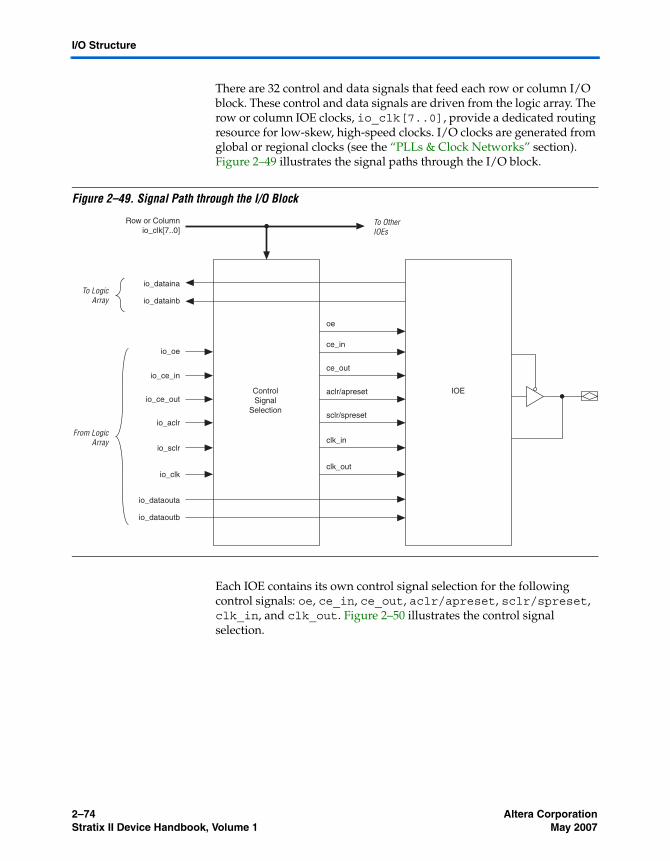
2–74 Altera CorporationStratix II Device Handbook, Volume 1 May 2007
I/O Structure
There are 32 control and data signals that feed each row or column I/O block. These control and data signals are driven from the logic array. The row or column IOE clocks, io_clk[7..0], provide a dedicated routing resource for low-skew, high-speed clocks. I/O clocks are generated from global or regional clocks (see the “PLLs & Clock Networks” section). Figure 2–49 illustrates the signal paths through the I/O block.
Figure 2–49. Signal Path through the I/O Block
Each IOE contains its own control signal selection for the following control signals: oe, ce_in, ce_out, aclr/apreset, sclr/spreset, clk_in, and clk_out. Figure 2–50 illustrates the control signal selection.
Row or Columnio_clk[7..0]
io_dataina
io_datainb
io_dataouta
io_dataoutb
io_oe
oe
ce_in
ce_outio_ce_in
aclr/apresetio_ce_out
sclr/spreset
io_sclr
io_aclr
clk_in
io_clkclk_out
ControlSignal
Selection
IOE
To LogicArray
From LogicArray
To OtherIOEs
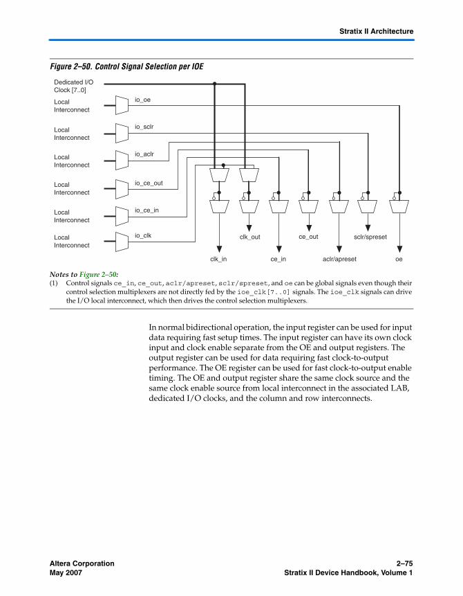
Altera Corporation 2–75May 2007 Stratix II Device Handbook, Volume 1
Stratix II Architecture
Figure 2–50. Control Signal Selection per IOE
Notes to Figure 2–50:(1) Control signals ce_in, ce_out, aclr/apreset, sclr/spreset, and oe can be global signals even though their
control selection multiplexers are not directly fed by the ioe_clk[7..0] signals. The ioe_clk signals can drive the I/O local interconnect, which then drives the control selection multiplexers.
In normal bidirectional operation, the input register can be used for input data requiring fast setup times. The input register can have its own clock input and clock enable separate from the OE and output registers. The output register can be used for data requiring fast clock-to-output performance. The OE register can be used for fast clock-to-output enable timing. The OE and output register share the same clock source and the same clock enable source from local interconnect in the associated LAB, dedicated I/O clocks, and the column and row interconnects.
clk_out
ce_inclk_in
ce_out
aclr/apreset
sclr/spreset
Dedicated I/OClock [7..0]
LocalInterconnect
LocalInterconnect
LocalInterconnect
LocalInterconnect
LocalInterconnect
oe
io_oe
io_aclr
LocalInterconnect
io_sclr
io_ce_out
io_ce_in
io_clk
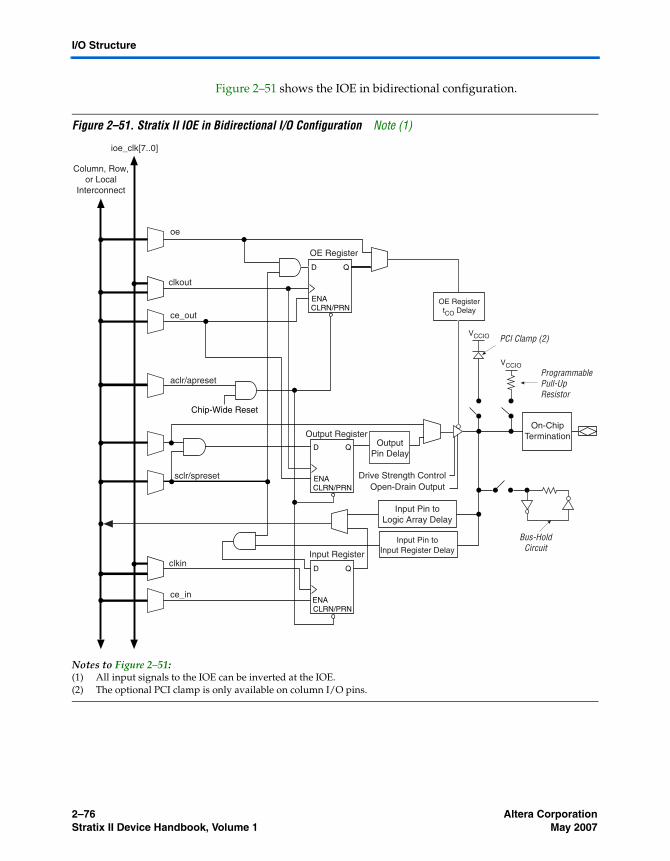
2–76 Altera CorporationStratix II Device Handbook, Volume 1 May 2007
I/O Structure
Figure 2–51 shows the IOE in bidirectional configuration.
Figure 2–51. Stratix II IOE in Bidirectional I/O Configuration Note (1)
Notes to Figure 2–51:(1) All input signals to the IOE can be inverted at the IOE.(2) The optional PCI clamp is only available on column I/O pins.
CLRN/PRN
D Q
ENA
Chip-Wide Reset
OE Register
CLRN/PRN
D Q
ENA
Output Register
VCCIO
VCCIO PCI Clamp (2)
ProgrammablePull-UpResistor
Column, Row,or Local
Interconnect
ioe_clk[7..0]
Bus-HoldCircuit
OE RegistertCO Delay
CLRN/PRN
D Q
ENA
Input Register
Input Pin toInput Register Delay
Input Pin toLogic Array Delay
Drive Strength ControlOpen-Drain Output
On-ChipTermination
sclr/spreset
oe
clkout
ce_out
aclr/apreset
clkin
ce_in
OutputPin Delay
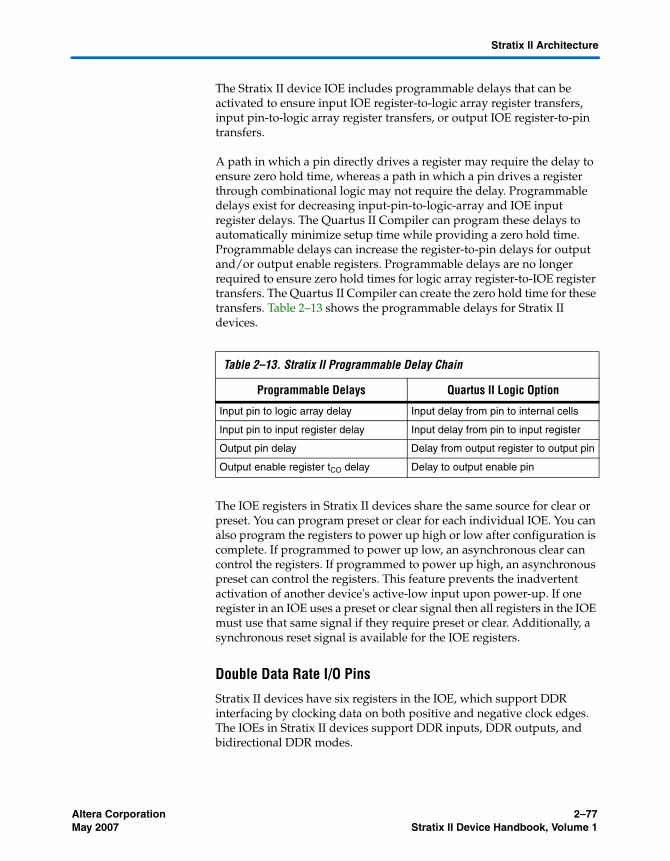
Altera Corporation 2–77May 2007 Stratix II Device Handbook, Volume 1
Stratix II Architecture
The Stratix II device IOE includes programmable delays that can be activated to ensure input IOE register-to-logic array register transfers, input pin-to-logic array register transfers, or output IOE register-to-pin transfers.
A path in which a pin directly drives a register may require the delay to ensure zero hold time, whereas a path in which a pin drives a register through combinational logic may not require the delay. Programmable delays exist for decreasing input-pin-to-logic-array and IOE input register delays. The Quartus II Compiler can program these delays to automatically minimize setup time while providing a zero hold time. Programmable delays can increase the register-to-pin delays for output and/or output enable registers. Programmable delays are no longer required to ensure zero hold times for logic array register-to-IOE register transfers. The Quartus II Compiler can create the zero hold time for these transfers. Table 2–13 shows the programmable delays for Stratix II devices.
The IOE registers in Stratix II devices share the same source for clear or preset. You can program preset or clear for each individual IOE. You can also program the registers to power up high or low after configuration is complete. If programmed to power up low, an asynchronous clear can control the registers. If programmed to power up high, an asynchronous preset can control the registers. This feature prevents the inadvertent activation of another device's active-low input upon power-up. If one register in an IOE uses a preset or clear signal then all registers in the IOE must use that same signal if they require preset or clear. Additionally, a synchronous reset signal is available for the IOE registers.
Double Data Rate I/O Pins
Stratix II devices have six registers in the IOE, which support DDR interfacing by clocking data on both positive and negative clock edges. The IOEs in Stratix II devices support DDR inputs, DDR outputs, and bidirectional DDR modes.
Table 2–13. Stratix II Programmable Delay Chain
Programmable Delays Quartus II Logic Option
Input pin to logic array delay Input delay from pin to internal cells
Input pin to input register delay Input delay from pin to input register
Output pin delay Delay from output register to output pin
Output enable register tCO delay Delay to output enable pin
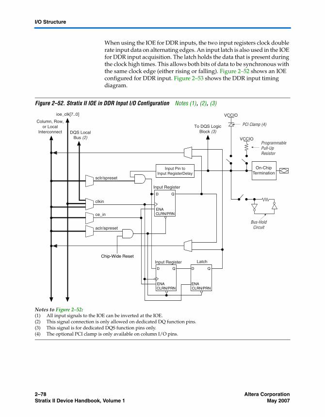
2–78 Altera CorporationStratix II Device Handbook, Volume 1 May 2007
I/O Structure
When using the IOE for DDR inputs, the two input registers clock double rate input data on alternating edges. An input latch is also used in the IOE for DDR input acquisition. The latch holds the data that is present during the clock high times. This allows both bits of data to be synchronous with the same clock edge (either rising or falling). Figure 2–52 shows an IOE configured for DDR input. Figure 2–53 shows the DDR input timing diagram.
Figure 2–52. Stratix II IOE in DDR Input I/O Configuration Notes (1), (2), (3)
Notes to Figure 2–52:(1) All input signals to the IOE can be inverted at the IOE.(2) This signal connection is only allowed on dedicated DQ function pins.(3) This signal is for dedicated DQS function pins only.(4) The optional PCI clamp is only available on column I/O pins.
CLRN/PRN
D Q
ENA
Chip-Wide Reset
Input Register
CLRN/PRN
D Q
ENA
Input Register
VCCIO
VCCIO
PCI Clamp (4)
ProgrammablePull-UpResistor
Column, Row,or Local
Interconnect DQS LocalBus (2)
To DQS LogicBlock (3)
ioe_clk[7..0]
Bus-HoldCircuit
CLRN/PRN
D Q
ENA
Latch
Input Pin toInput RegisterDelay
sclr/spreset
clkin
aclr/apreset
On-ChipTermination
ce_in
Altera Corporation 2–79May 2007 Stratix II Device Handbook, Volume 1
Stratix II Architecture
Figure 2–53. Input Timing Diagram in DDR Mode
When using the IOE for DDR outputs, the two output registers are configured to clock two data paths from ALMs on rising clock edges. These output registers are multiplexed by the clock to drive the output pin at a ×2 rate. One output register clocks the first bit out on the clock high time, while the other output register clocks the second bit out on the clock low time. Figure 2–54 shows the IOE configured for DDR output. Figure 2–55 shows the DDR output timing diagram.
Data atinput pin
CLK
A0B0 B1 A1
A1
B2 A2 A3
A2 A3
B1
A0
B0 B2 B3
B3 B4
Input ToLogic Array
2–80 Altera CorporationStratix II Device Handbook, Volume 1 May 2007
I/O Structure
Figure 2–54. Stratix II IOE in DDR Output I/O Configuration Notes (1), (2)
Notes to Figure 2–54:(1) All input signals to the IOE can be inverted at the IOE.(2) The tri-state buffer is active low. The DDIO megafunction represents the tri-state buffer as active-high with an
inverter at the OE register data port. Similarly, the aclr and apreset signals are also active-high at the input ports of the DDIO megafunction.
(3) The optional PCI clamp is only available on column I/O pins.
CLRN/PRN
D Q
ENA
Chip-Wide Reset
OE Register
CLRN/PRN
D Q
ENA
OE Register
CLRN/PRN
D Q
ENA
Output Register
VCCIO
VCCIO
PCI Clamp (3)
ProgrammablePull-UpResistor
Column, Row,or Local
Interconnect
ioe_clk[7..0]
Bus-HoldCircuit
OE RegistertCO Delay
CLRN/PRN
D Q
ENA
Output Register
Drive StrengthControl
Open-Drain Output
Used forDDR, DDR2SDRAM
sclr/spreset
aclr/apreset
clkout
OutputPin Delay
On-ChipTermination
oe
ce_out
clk
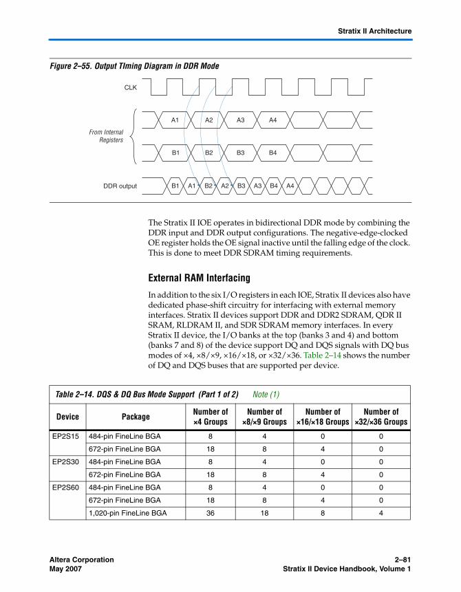
Altera Corporation 2–81May 2007 Stratix II Device Handbook, Volume 1
Stratix II Architecture
Figure 2–55. Output TIming Diagram in DDR Mode
The Stratix II IOE operates in bidirectional DDR mode by combining the DDR input and DDR output configurations. The negative-edge-clocked OE register holds the OE signal inactive until the falling edge of the clock. This is done to meet DDR SDRAM timing requirements.
External RAM Interfacing
In addition to the six I/O registers in each IOE, Stratix II devices also have dedicated phase-shift circuitry for interfacing with external memory interfaces. Stratix II devices support DDR and DDR2 SDRAM, QDR II SRAM, RLDRAM II, and SDR SDRAM memory interfaces. In every Stratix II device, the I/O banks at the top (banks 3 and 4) and bottom (banks 7 and 8) of the device support DQ and DQS signals with DQ bus modes of ×4, ×8/×9, ×16/×18, or ×32/×36. Table 2–14 shows the number of DQ and DQS buses that are supported per device.
From InternalRegisters
DDR output
CLK
B1 A1 B2 A2 B3 A3 B4 A4
A2A1 A3 A4
B1 B2 B3 B4
Table 2–14. DQS & DQ Bus Mode Support (Part 1 of 2) Note (1)
Device Package Number of ×4 Groups
Number of ×8/×9 Groups
Number of ×16/×18 Groups
Number of ×32/×36 Groups
EP2S15 484-pin FineLine BGA 8 4 0 0
672-pin FineLine BGA 18 8 4 0
EP2S30 484-pin FineLine BGA 8 4 0 0
672-pin FineLine BGA 18 8 4 0
EP2S60 484-pin FineLine BGA 8 4 0 0
672-pin FineLine BGA 18 8 4 0
1,020-pin FineLine BGA 36 18 8 4

2–82 Altera CorporationStratix II Device Handbook, Volume 1 May 2007
I/O Structure
A compensated delay element on each DQS pin automatically aligns input DQS synchronization signals with the data window of their corresponding DQ data signals. The DQS signals drive a local DQS bus in the top and bottom I/O banks. This DQS bus is an additional resource to the I/O clocks and is used to clock DQ input registers with the DQS signal.
The Stratix II device has two phase-shifting reference circuits, one on the top and one on the bottom of the device. The circuit on the top controls the compensated delay elements for all DQS pins on the top. The circuit on the bottom controls the compensated delay elements for all DQS pins on the bottom.
Each phase-shifting reference circuit is driven by a system reference clock, which must have the same frequency as the DQS signal. Clock pins CLK[15..12]p feed the phase circuitry on the top of the device and clock pins CLK[7..4]p feed the phase circuitry on the bottom of the device. In addition, PLL clock outputs can also feed the phase-shifting reference circuits.
Figure 2–56 illustrates the phase-shift reference circuit control of each DQS delay shift on the top of the device. This same circuit is duplicated on the bottom of the device.
EP2S90 484-pin Hybrid FineLine BGA 8 4 0 0
780-pin FineLine BGA 18 8 4 0
1,020-pin FineLine BGA 36 18 8 4
1,508-pin FineLine BGA 36 18 8 4
EP2S130 780-pin FineLine BGA 18 8 4 0
1,020-pin FineLine BGA 36 18 8 4
1,508-pin FineLine BGA 36 18 8 4
EP2S180 1,020-pin FineLine BGA 36 18 8 4
1,508-pin FineLine BGA 36 18 8 4
Notes to Table 2–14:(1) Check the pin table for each DQS/DQ group in the different modes.
Table 2–14. DQS & DQ Bus Mode Support (Part 2 of 2) Note (1)
Device Package Number of ×4 Groups
Number of ×8/×9 Groups
Number of ×16/×18 Groups
Number of ×32/×36 Groups
Altera Corporation 2–83May 2007 Stratix II Device Handbook, Volume 1
Stratix II Architecture
Figure 2–56. DQS Phase-Shift Circuitry Notes (1), (2), (3), (4)
Notes to Figure 2–56:(1) There are up to 18 pairs of DQS and DQSn pins available on the top or the bottom of the Stratix II device. There are
up to 10 pairs on the right side and 8 pairs on the left side of the DQS phase-shift circuitry.(2) The Δt module represents the DQS logic block.(3) Clock pins CLK[15..12]p feed the phase-shift circuitry on the top of the device and clock pins CLK[7..4]p feed
the phase circuitry on the bottom of the device. You can also use a PLL clock output as a reference clock to the phase-shift circuitry.
(4) You can only use PLL 5 to feed the DQS phase-shift circuitry on the top of the device and PLL 6 to feed the DQS phase-shift circuitry on the bottom of the device.
These dedicated circuits combined with enhanced PLL clocking and phase-shift ability provide a complete hardware solution for interfacing to high-speed memory.
f For more information on external memory interfaces, refer to the External Memory Interfaces in Stratix II & Stratix II GX Devices chapter in volume 2 of the Stratix II Device Handbook or the Stratix II GX Device Handbook.
Programmable Drive Strength
The output buffer for each Stratix II device I/O pin has a programmable drive strength control for certain I/O standards. The LVTTL, LVCMOS, SSTL, and HSTL standards have several levels of drive strength that the user can control. The default setting used in the Quartus II software is the maximum current strength setting that is used to achieve maximum I/O performance. For all I/O standards, the minimum setting is the lowest drive strength that guarantees the IOH/IOL of the standard. Using minimum settings provides signal slew rate control to reduce system noise and signal overshoot.
DQSPin
DQSnPin
DQSnPin
DQSPin
DQSPin
DQSnPin
DQSPin
DQSnPin
From PLL 5 (3)
CLK[15..12]p (2)
to IOE to IOE to IOE to IOEto IOE to IOEto IOE
ΔtΔtΔtΔtΔtΔt Δt
to IOE
DQSPhase-Shift
CircuitryΔt DQS Logic
Blocks
2–84 Altera CorporationStratix II Device Handbook, Volume 1 May 2007
I/O Structure
Table 2–15 shows the possible settings for the I/O standards with drive strength control.
Open-Drain Output
Stratix II devices provide an optional open-drain (equivalent to an open-collector) output for each I/O pin. This open-drain output enables the device to provide system-level control signals (e.g., interrupt and write-enable signals) that can be asserted by any of several devices.
Bus Hold
Each Stratix II device I/O pin provides an optional bus-hold feature. The bus-hold circuitry can weakly hold the signal on an I/O pin at its last-driven state. Since the bus-hold feature holds the last-driven state of the pin until the next input signal is present, you do not need an external pull-up or pull-down resistor to hold a signal level when the bus is tri-stated.
Table 2–15. Programmable Drive Strength Note (1)
I/O StandardIOH / IOL Current Strength Setting (mA) for Column
I/O Pins
IOH / IOL Current Strength Setting (mA) for Row I/O
Pins
3.3-V LVTTL 24, 20, 16, 12, 8, 4 12, 8, 4
3.3-V LVCMOS 24, 20, 16, 12, 8, 4 8, 4
2.5-V LVTTL/LVCMOS 16, 12, 8, 4 12, 8, 4
1.8-V LVTTL/LVCMOS 12, 10, 8, 6, 4, 2 8, 6, 4, 2
1.5-V LVCMOS 8, 6, 4, 2 4, 2
SSTL-2 Class I 12, 8 12, 8
SSTL-2 Class II 24, 20, 16 16
SSTL-18 Class I 12, 10, 8, 6, 4 10, 8, 6, 4
SSTL-18 Class II 20, 18, 16, 8 -
HSTL-18 Class I 12, 10, 8, 6, 4 12, 10, 8, 6, 4
HSTL-18 Class II 20, 18, 16 -
HSTL-15 Class I 12, 10, 8, 6, 4 8, 6, 4
HSTL-15 Class II 20, 18, 16 -
Note to Table 2–15:(1) The Quartus II software default current setting is the maximum setting for each
I/O standard.
Altera Corporation 2–85May 2007 Stratix II Device Handbook, Volume 1
Stratix II Architecture
The bus-hold circuitry also pulls undriven pins away from the input threshold voltage where noise can cause unintended high-frequency switching. You can select this feature individually for each I/O pin. The bus-hold output drives no higher than VCCIO to prevent overdriving signals. If the bus-hold feature is enabled, the programmable pull-up option cannot be used. Disable the bus-hold feature when the I/O pin has been configured for differential signals.
The bus-hold circuitry uses a resistor with a nominal resistance (RBH) of approximately 7 kΩ to weakly pull the signal level to the last-driven state. See the DC & Switching Characteristics chapter in the Stratix II Device Handbook, Volume 1, for the specific sustaining current driven through this resistor and overdrive current used to identify the next-driven input level. This information is provided for each VCCIO voltage level.
The bus-hold circuitry is active only after configuration. When going into user mode, the bus-hold circuit captures the value on the pin present at the end of configuration.
Programmable Pull-Up Resistor
Each Stratix II device I/O pin provides an optional programmable pull-up resistor during user mode. If you enable this feature for an I/O pin, the pull-up resistor (typically 25 kΩ) weakly holds the output to the VCCIO level of the output pin’s bank.
Programmable pull-up resistors are only supported on user I/O pins, and are not supported on dedicated configuration pins, JTAG pins or dedicated clock pins.
Advanced I/O Standard Support
Stratix II device IOEs support the following I/O standards:
■ 3.3-V LVTTL/LVCMOS■ 2.5-V LVTTL/LVCMOS■ 1.8-V LVTTL/LVCMOS■ 1.5-V LVCMOS■ 3.3-V PCI■ 3.3-V PCI-X mode 1■ LVDS■ LVPECL (on input and output clocks only)■ HyperTransport technology■ Differential 1.5-V HSTL Class I and II■ Differential 1.8-V HSTL Class I and II■ Differential SSTL-18 Class I and II■ Differential SSTL-2 Class I and II
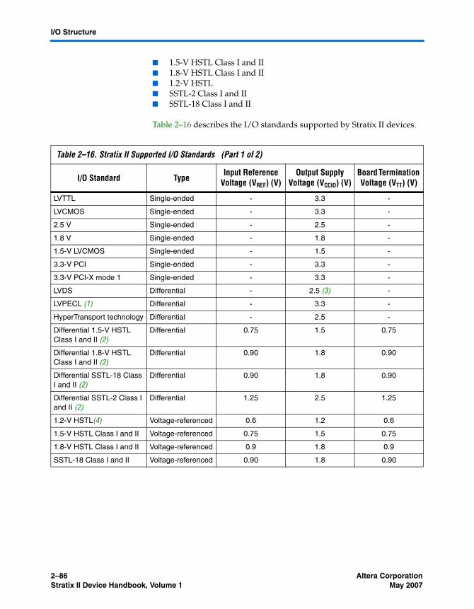
2–86 Altera CorporationStratix II Device Handbook, Volume 1 May 2007
I/O Structure
■ 1.5-V HSTL Class I and II■ 1.8-V HSTL Class I and II■ 1.2-V HSTL■ SSTL-2 Class I and II■ SSTL-18 Class I and II
Table 2–16 describes the I/O standards supported by Stratix II devices.
Table 2–16. Stratix II Supported I/O Standards (Part 1 of 2)
I/O Standard TypeInput Reference
Voltage (VREF) (V)Output Supply
Voltage (VCCIO) (V)Board Termination Voltage (VTT) (V)
LVTTL Single-ended - 3.3 -
LVCMOS Single-ended - 3.3 -
2.5 V Single-ended - 2.5 -
1.8 V Single-ended - 1.8 -
1.5-V LVCMOS Single-ended - 1.5 -
3.3-V PCI Single-ended - 3.3 -
3.3-V PCI-X mode 1 Single-ended - 3.3 -
LVDS Differential - 2.5 (3) -
LVPECL (1) Differential - 3.3 -
HyperTransport technology Differential - 2.5 -
Differential 1.5-V HSTL Class I and II (2)
Differential 0.75 1.5 0.75
Differential 1.8-V HSTL Class I and II (2)
Differential 0.90 1.8 0.90
Differential SSTL-18 Class I and II (2)
Differential 0.90 1.8 0.90
Differential SSTL-2 Class I and II (2)
Differential 1.25 2.5 1.25
1.2-V HSTL(4) Voltage-referenced 0.6 1.2 0.6
1.5-V HSTL Class I and II Voltage-referenced 0.75 1.5 0.75
1.8-V HSTL Class I and II Voltage-referenced 0.9 1.8 0.9
SSTL-18 Class I and II Voltage-referenced 0.90 1.8 0.90
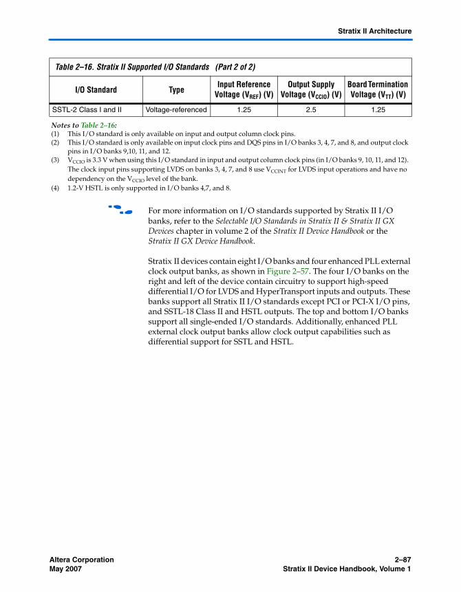
Altera Corporation 2–87May 2007 Stratix II Device Handbook, Volume 1
Stratix II Architecture
f For more information on I/O standards supported by Stratix II I/O banks, refer to the Selectable I/O Standards in Stratix II & Stratix II GX Devices chapter in volume 2 of the Stratix II Device Handbook or the Stratix II GX Device Handbook.
Stratix II devices contain eight I/O banks and four enhanced PLL external clock output banks, as shown in Figure 2–57. The four I/O banks on the right and left of the device contain circuitry to support high-speed differential I/O for LVDS and HyperTransport inputs and outputs. These banks support all Stratix II I/O standards except PCI or PCI-X I/O pins, and SSTL-18 Class II and HSTL outputs. The top and bottom I/O banks support all single-ended I/O standards. Additionally, enhanced PLL external clock output banks allow clock output capabilities such as differential support for SSTL and HSTL.
SSTL-2 Class I and II Voltage-referenced 1.25 2.5 1.25
Notes to Table 2–16:(1) This I/O standard is only available on input and output column clock pins.(2) This I/O standard is only available on input clock pins and DQS pins in I/O banks 3, 4, 7, and 8, and output clock
pins in I/O banks 9,10, 11, and 12.(3) VCCIO is 3.3 V when using this I/O standard in input and output column clock pins (in I/O banks 9, 10, 11, and 12).
The clock input pins supporting LVDS on banks 3, 4, 7, and 8 use VCCINT for LVDS input operations and have no dependency on the VCCIO level of the bank.
(4) 1.2-V HSTL is only supported in I/O banks 4,7, and 8.
Table 2–16. Stratix II Supported I/O Standards (Part 2 of 2)
I/O Standard TypeInput Reference
Voltage (VREF) (V)Output Supply
Voltage (VCCIO) (V)Board Termination Voltage (VTT) (V)
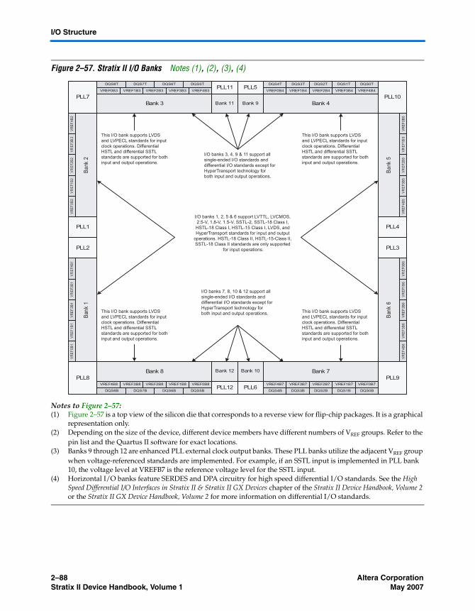
2–88 Altera CorporationStratix II Device Handbook, Volume 1 May 2007
I/O Structure
Figure 2–57. Stratix II I/O Banks Notes (1), (2), (3), (4)
Notes to Figure 2–57:(1) Figure 2–57 is a top view of the silicon die that corresponds to a reverse view for flip-chip packages. It is a graphical
representation only. (2) Depending on the size of the device, different device members have different numbers of VREF groups. Refer to the
pin list and the Quartus II software for exact locations.(3) Banks 9 through 12 are enhanced PLL external clock output banks. These PLL banks utilize the adjacent VREF group
when voltage-referenced standards are implemented. For example, if an SSTL input is implemented in PLL bank 10, the voltage level at VREFB7 is the reference voltage level for the SSTL input.
(4) Horizontal I/O banks feature SERDES and DPA circuitry for high speed differential I/O standards. See the High Speed Differential I/O Interfaces in Stratix II & Stratix II GX Devices chapter of the Stratix II Device Handbook, Volume 2 or the Stratix II GX Device Handbook, Volume 2 for more information on differential I/O standards.
Bank 3 Bank 4Bank 11 Bank 9
PLL11 PLL5
PLL7
PLL1
PLL2
PLL4
PLL3
PLL10
I/O banks 7, 8, 10 & 12 support all
single-ended I/O standards and
differential I/O standards except for
HyperTransport technology for
both input and output operations.
I/O banks 3, 4, 9 & 11 support all
single-ended I/O standards and
differential I/O standards except for
HyperTransport technology for
both input and output operations.
VREF0B3 VREF1B3 VREF2B3 VREF3B3 VREF4B3 VREF0B4 VREF1B4 VREF2B4 VREF3B4 VREF4B4
Bank 8 Bank 7Bank 12 Bank 10
PLL12 PLL6
PLL8 PLL9VREF4B8 VREF3B8 VREF2B8 VREF1B8 VREF0B8 VREF4B7 VREF3B7 VREF2B7 VREF1B7 VREF0B7
VR
EF
3B
2V
RE
F2
B2
VR
EF
1B
2V
RE
F0
B2
Ba
nk 2
VR
EF
3B
1V
RE
F2
B1
VR
EF
1B
1V
RE
F0
B1
Ban
k 1
VR
EF
1B
5V
RE
F2
B5
VR
EF
3B
5V
RE
F4
B5
Ba
nk 5
VR
EF
1B
6V
RE
F2
B6
VR
EF
3B
6V
RE
F4
B6
Ban
k 6
VR
EF
4B
2
VR
EF
0B
5
VR
EF
4B
1
VR
EF
0B
6
DQS4T DQS3T DQS2T DQS1T DQS0T
DQS4B DQS3B DQS2B DQS1B DQS0BDQS8B DQS7B DQS6B DQS5B
DQS8T DQS7T DQS6T DQS5T
This I/O bank supports LVDS
and LVPECL standards for input
clock operations. Differential
HSTL and differential SSTL
standards are supported for both
input and output operations.
This I/O bank supports LVDS
and LVPECL standards for input
clock operations. Differential
HSTL and differential SSTL
standards are supported for both
input and output operations.
This I/O bank supports LVDS
and LVPECL standards for input
clock operations. Differential
HSTL and differential SSTL
standards are supported for both
input and output operations.
This I/O bank supports LVDS
and LVPECL standards for input
clock operations. Differential
HSTL and differential SSTL
standards are supported for both
input and output operations.
I/O banks 1, 2, 5 & 6 support LVTTL, LVCMOS,
2.5-V, 1.8-V, 1.5-V, SSTL-2, SSTL-18 Class I,
HSTL-18 Class I, HSTL-15 Class I, LVDS, and
HyperTransport standards for input and output
operations. HSTL-18 Class II, HSTL-15-Class II,
SSTL-18 Class II standards are only supported
for input operations.
Altera Corporation 2–89May 2007 Stratix II Device Handbook, Volume 1
Stratix II Architecture
Each I/O bank has its own VCCIO pins. A single device can support 1.5-, 1.8-, 2.5-, and 3.3-V interfaces; each bank can support a different VCCIO level independently. Each bank also has dedicated VREF pins to support the voltage-referenced standards (such as SSTL-2). The PLL banks utilize the adjacent VREF group when voltage-referenced standards are implemented. For example, if an SSTL input is implemented in PLL bank 10, the voltage level at VREFB7 is the reference voltage level for the SSTL input.
I/O pins that reside in PLL banks 9 through 12 are powered by the VCC_PLL<5, 6, 11, or 12>_OUT pins, respectively. The EP2S60F484, EP2S60F780, EP2S90H484, EP2S90F780, and EP2S130F780 devices do not support PLLs 11 and 12. Therefore, any I/O pins that reside in bank 11 are powered by the VCCIO3 pin, and any I/O pins that reside in bank 12 are powered by the VCCIO8 pin.
Each I/O bank can support multiple standards with the same VCCIO for input and output pins. Each bank can support one VREF voltage level. For example, when VCCIO is 3.3 V, a bank can support LVTTL, LVCMOS, and 3.3-V PCI for inputs and outputs.
On-Chip Termination
Stratix II devices provide differential (for the LVDS or HyperTransport technology I/O standard), series, and parallel on-chip termination to reduce reflections and maintain signal integrity. On-chip termination simplifies board design by minimizing the number of external termination resistors required. Termination can be placed inside the package, eliminating small stubs that can still lead to reflections.
Stratix II devices provide four types of termination:
■ Differential termination (RD)■ Series termination (RS) without calibration■ Series termination (RS) with calibration■ Parallel termination (RT) with calibration
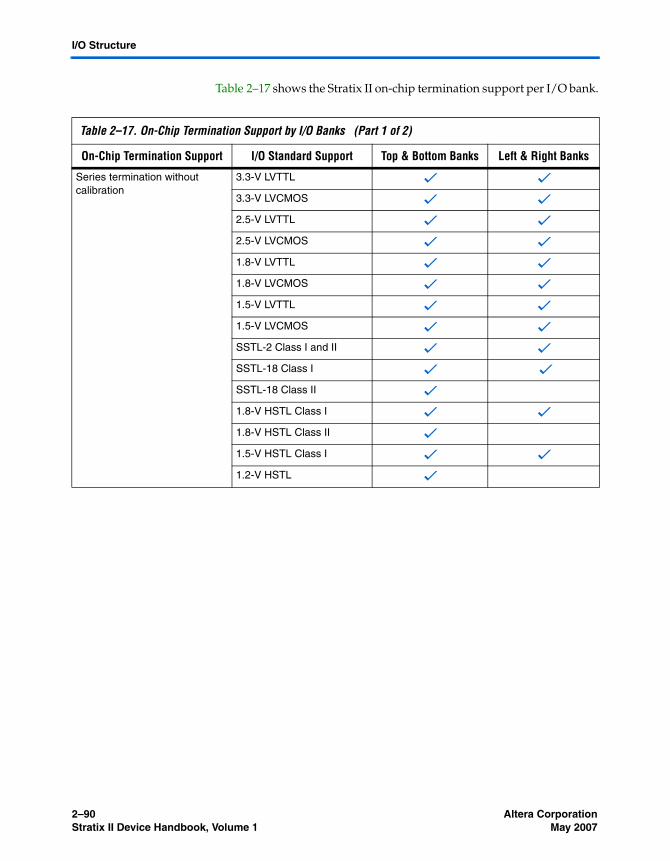
2–90 Altera CorporationStratix II Device Handbook, Volume 1 May 2007
I/O Structure
Table 2–17 shows the Stratix II on-chip termination support per I/O bank.
Table 2–17. On-Chip Termination Support by I/O Banks (Part 1 of 2)
On-Chip Termination Support I/O Standard Support Top & Bottom Banks Left & Right Banks
Series termination without calibration
3.3-V LVTTL v v
3.3-V LVCMOS v v
2.5-V LVTTL v v
2.5-V LVCMOS v v
1.8-V LVTTL v v
1.8-V LVCMOS v v
1.5-V LVTTL v v
1.5-V LVCMOS v v
SSTL-2 Class I and II v v
SSTL-18 Class I v v
SSTL-18 Class II v
1.8-V HSTL Class I v v
1.8-V HSTL Class II v
1.5-V HSTL Class I v v
1.2-V HSTL v
Altera Corporation 2–91May 2007 Stratix II Device Handbook, Volume 1
Stratix II Architecture
Series termination with calibration
3.3-V LVTTL v
3.3-V LVCMOS v
2.5-V LVTTL v
2.5-V LVCMOS v
1.8-V LVTTL v
1.8-V LVCMOS v
1.5-V LVTTL v
1.5-V LVCMOS v
SSTL-2 Class I and II v
SSTL-18 Class I and II v
1.8-V HSTL Class I v
1.8-V HSTL Class II v
1.5-V HSTL Class I v
1.2-V HSTL v
Parallel termination with calibration
SSTL-2 Class I and II v
SSTL-18 Class I and II v
1.8-V HSTL Class I v
1.8-V HSTL Class II v
1.5-V HSTL Class I and II v
1.2-V HSTL v
Differential termination (1) LVDS v
HyperTransport technology v
Note to Table 2–17:(1) Clock pins CLK1, CLK3, CLK9, CLK11, and pins FPLL[7..10]CLK do not support differential on-chip
termination. Clock pins CLK0, CLK2, CLK8, and CLK10 do support differential on-chip termination. Clock pins in the top and bottom banks (CLK[4..7, 12..15]) do not support differential on-chip termination.
Table 2–17. On-Chip Termination Support by I/O Banks (Part 2 of 2)
On-Chip Termination Support I/O Standard Support Top & Bottom Banks Left & Right Banks
2–92 Altera CorporationStratix II Device Handbook, Volume 1 May 2007
I/O Structure
Differential On-Chip Termination
Stratix II devices support internal differential termination with a nominal resistance value of 100 Ω for LVDS or HyperTransport technology input receiver buffers. LVPECL input signals (supported on clock pins only) require an external termination resistor. Differential on-chip termination is supported across the full range of supported differential data rates as shown in the DC & Switching Characteristics chapter in volume 1 of the Stratix II Device Handbook.
f For more information on differential on-chip termination, refer to the High-Speed Differential I/O Interfaces with DPA in Stratix II & Stratix II GX Devices chapter in volume 2 of the Stratix II Device Handbook or the Stratix II GX Device Handbook.
f For more information on tolerance specifications for differential on-chip termination, refer to the DC & Switching Characteristics chapter in volume 1 of the Stratix II Device Handbook.
On-Chip Series Termination Without Calibration
Stratix II devices support driver impedance matching to provide the I/O driver with controlled output impedance that closely matches the impedance of the transmission line. As a result, reflections can be significantly reduced. Stratix II devices support on-chip series termination for single-ended I/O standards with typical RS values of 25 and 50 Ω. Once matching impedance is selected, current drive strength is no longer selectable. Table 2–17 shows the list of output standards that support on-chip series termination without calibration.
On-Chip Series Termination with Calibration
Stratix II devices support on-chip series termination with calibration in column I/O pins in top and bottom banks. There is one calibration circuit for the top I/O banks and one circuit for the bottom I/O banks. Each on-chip series termination calibration circuit compares the total impedance of each I/O buffer to the external 25- or 50-Ω resistors connected to the RUP and RDN pins, and dynamically enables or disables the transistors until they match. Calibration occurs at the end of device configuration. Once the calibration circuit finds the correct impedance, it powers down and stops changing the characteristics of the drivers.
f For more information on series on-chip termination supported by Stratix II devices, refer to the Selectable I/O Standards in Stratix II & Stratix II GX Devices chapter in volume 2 of the Stratix II Device Handbook or the Stratix II GX Device Handbook.
Altera Corporation 2–93May 2007 Stratix II Device Handbook, Volume 1
Stratix II Architecture
f For more information on tolerance specifications for on-chip termination with calibration, refer to the DC & Switching Characteristics chapter in volume 1 of the Stratix II Device Handbook.
On-Chip Parallel Termination with Calibration
Stratix II devices support on-chip parallel termination with calibration for column I/O pins only. There is one calibration circuit for the top I/O banks and one circuit for the bottom I/O banks. Each on-chip parallel termination calibration circuit compares the total impedance of each I/O buffer to the external 50-Ω resistors connected to the RUP and RDN pins and dynamically enables or disables the transistors until they match. Calibration occurs at the end of device configuration. Once the calibration circuit finds the correct impedance, it powers down and stops changing the characteristics of the drivers.
1 On-chip parallel termination with calibration is only supported for input pins.
f For more information on on-chip termination supported by Stratix II devices, refer to the Selectable I/O Standards in Stratix II & Stratix II GX Devices chapter in volume 2 of the Stratix II Device Handbook or the Stratix II GX Device Handbook.
f For more information on tolerance specifications for on-chip termination with calibration, refer to the DC & Switching Characteristics chapter in volume 1 of the Stratix II Device Handbook.
MultiVolt I/O Interface
The Stratix II architecture supports the MultiVolt I/O interface feature that allows Stratix II devices in all packages to interface with systems of different supply voltages.
The Stratix II VCCINT pins must always be connected to a 1.2-V power supply. With a 1.2-V VCCINT level, input pins are 1.5-, 1.8-, 2.5-, and 3.3-V tolerant. The VCCIO pins can be connected to either a 1.5-, 1.8-, 2.5-, or 3.3-V power supply, depending on the output requirements. The output levels are compatible with systems of the same voltage as the power supply (for example, when VCCIO pins are connected to a 1.5-V power supply, the output levels are compatible with 1.5-V systems).
The Stratix II VCCPD power pins must be connected to a 3.3-V power supply. These power pins are used to supply the pre-driver power to the output buffers, which increases the performance of the output pins. The VCCPD pins also power configuration input pins and JTAG input pins.
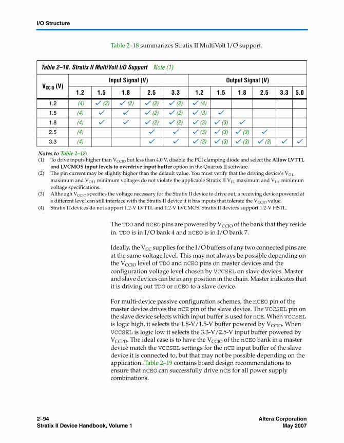
2–94 Altera CorporationStratix II Device Handbook, Volume 1 May 2007
I/O Structure
Table 2–18 summarizes Stratix II MultiVolt I/O support.
The TDO and nCEO pins are powered by VCCIO of the bank that they reside in. TDO is in I/O bank 4 and nCEO is in I/O bank 7.
Ideally, the VCC supplies for the I/O buffers of any two connected pins are at the same voltage level. This may not always be possible depending on the VCCIO level of TDO and nCEO pins on master devices and the configuration voltage level chosen by VCCSEL on slave devices. Master and slave devices can be in any position in the chain. Master indicates that it is driving out TDO or nCEO to a slave device.
For multi-device passive configuration schemes, the nCEO pin of the master device drives the nCE pin of the slave device. The VCCSEL pin on the slave device selects which input buffer is used for nCE. When VCCSEL is logic high, it selects the 1.8-V/1.5-V buffer powered by VCCIO. When VCCSEL is logic low it selects the 3.3-V/2.5-V input buffer powered by VCCPD. The ideal case is to have the VCCIO of the nCEO bank in a master device match the VCCSEL settings for the nCE input buffer of the slave device it is connected to, but that may not be possible depending on the application. Table 2–19 contains board design recommendations to ensure that nCEO can successfully drive nCE for all power supply combinations.
Table 2–18. Stratix II MultiVolt I/O Support Note (1)
VCCIO (V)Input Signal (V) Output Signal (V)
1.2 1.5 1.8 2.5 3.3 1.2 1.5 1.8 2.5 3.3 5.0
1.2 (4) v (2) v (2) v (2) v (2) v (4)
1.5 (4) v v v (2) v (2) v (3) v
1.8 (4) v v v (2) v (2) v (3) v (3) v
2.5 (4) v v v (3) v (3) v (3) v
3.3 (4) v v v (3) v (3) v (3) v (3) v v
Notes to Table 2–18:(1) To drive inputs higher than VCCIO but less than 4.0 V, disable the PCI clamping diode and select the Allow LVTTL
and LVCMOS input levels to overdrive input buffer option in the Quartus II software.(2) The pin current may be slightly higher than the default value. You must verify that the driving device’s VO L
maximum and VO H minimum voltages do not violate the applicable Stratix II VI L maximum and VI H minimum voltage specifications.
(3) Although VCCIO specifies the voltage necessary for the Stratix II device to drive out, a receiving device powered at a different level can still interface with the Stratix II device if it has inputs that tolerate the VCCIO value.
(4) Stratix II devices do not support 1.2-V LVTTL and 1.2-V LVCMOS. Stratix II devices support 1.2-V HSTL.
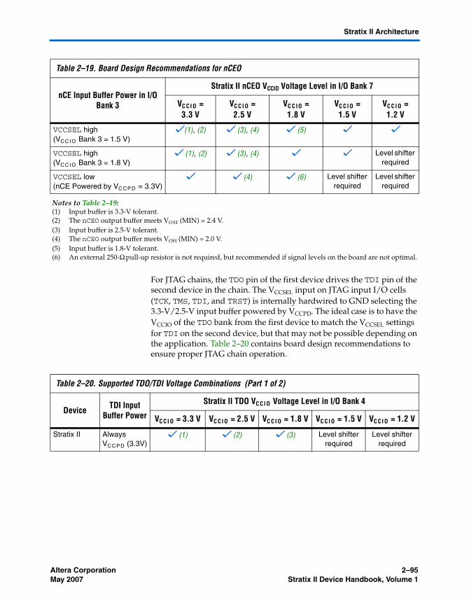
Altera Corporation 2–95May 2007 Stratix II Device Handbook, Volume 1
Stratix II Architecture
For JTAG chains, the TDO pin of the first device drives the TDI pin of the second device in the chain. The VCCSEL input on JTAG input I/O cells (TCK, TMS, TDI, and TRST) is internally hardwired to GND selecting the 3.3-V/2.5-V input buffer powered by VCCPD. The ideal case is to have the VCCIO of the TDO bank from the first device to match the VCCSEL settings for TDI on the second device, but that may not be possible depending on the application. Table 2–20 contains board design recommendations to ensure proper JTAG chain operation.
Table 2–19. Board Design Recommendations for nCEO
nCE Input Buffer Power in I/O Bank 3
Stratix II nCEO VCCIO Voltage Level in I/O Bank 7
VC C I O = 3.3 V
VC C I O =2.5 V
VC C I O =1.8 V
VC C I O =1.5 V
VC C I O =1.2 V
VCCSEL high (VC C I O Bank 3 = 1.5 V)
v(1), (2) v (3), (4) v (5) v v
VCCSEL high (VC C I O Bank 3 = 1.8 V)
v (1), (2) v (3), (4) v v Level shifter required
VCCSEL low (nCE Powered by VC CP D = 3.3V)
v v (4) v (6) Level shifter required
Level shifter required
Notes to Table 2–19:(1) Input buffer is 3.3-V tolerant.(2) The nCEO output buffer meets VO H (MIN) = 2.4 V.(3) Input buffer is 2.5-V tolerant.(4) The nCEO output buffer meets VOH (MIN) = 2.0 V.(5) Input buffer is 1.8-V tolerant.(6) An external 250-Ω pull-up resistor is not required, but recommended if signal levels on the board are not optimal.
Table 2–20. Supported TDO/TDI Voltage Combinations (Part 1 of 2)
Device TDI Input Buffer Power
Stratix II TDO VC C I O Voltage Level in I/O Bank 4
VC C I O = 3.3 V VC C I O = 2.5 V VC C I O = 1.8 V VC C I O = 1.5 V VC C I O = 1.2 V
Stratix II Always VC C P D (3.3V)
v (1) v (2) v (3) Level shifter required
Level shifter required
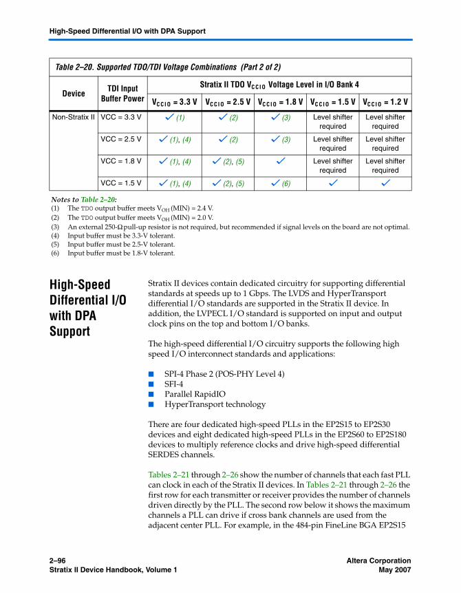
2–96 Altera CorporationStratix II Device Handbook, Volume 1 May 2007
High-Speed Differential I/O with DPA Support
High-Speed Differential I/O with DPA Support
Stratix II devices contain dedicated circuitry for supporting differential standards at speeds up to 1 Gbps. The LVDS and HyperTransport differential I/O standards are supported in the Stratix II device. In addition, the LVPECL I/O standard is supported on input and output clock pins on the top and bottom I/O banks.
The high-speed differential I/O circuitry supports the following high speed I/O interconnect standards and applications:
■ SPI-4 Phase 2 (POS-PHY Level 4)■ SFI-4■ Parallel RapidIO■ HyperTransport technology
There are four dedicated high-speed PLLs in the EP2S15 to EP2S30 devices and eight dedicated high-speed PLLs in the EP2S60 to EP2S180 devices to multiply reference clocks and drive high-speed differential SERDES channels.
Tables 2–21 through 2–26 show the number of channels that each fast PLL can clock in each of the Stratix II devices. In Tables 2–21 through 2–26 the first row for each transmitter or receiver provides the number of channels driven directly by the PLL. The second row below it shows the maximum channels a PLL can drive if cross bank channels are used from the adjacent center PLL. For example, in the 484-pin FineLine BGA EP2S15
Non-Stratix II VCC = 3.3 V v (1) v (2) v (3) Level shifter required
Level shifter required
VCC = 2.5 V v (1), (4) v (2) v (3) Level shifter required
Level shifter required
VCC = 1.8 V v (1), (4) v (2), (5) v Level shifter required
Level shifter required
VCC = 1.5 V v (1), (4) v (2), (5) v (6) v v
Notes to Table 2–20:(1) The TDO output buffer meets VOH (MIN) = 2.4 V.(2) The TDO output buffer meets VOH (MIN) = 2.0 V.(3) An external 250-Ω pull-up resistor is not required, but recommended if signal levels on the board are not optimal.(4) Input buffer must be 3.3-V tolerant.(5) Input buffer must be 2.5-V tolerant.(6) Input buffer must be 1.8-V tolerant.
Table 2–20. Supported TDO/TDI Voltage Combinations (Part 2 of 2)
Device TDI Input Buffer Power
Stratix II TDO VC C I O Voltage Level in I/O Bank 4
VC C I O = 3.3 V VC C I O = 2.5 V VC C I O = 1.8 V VC C I O = 1.5 V VC C I O = 1.2 V
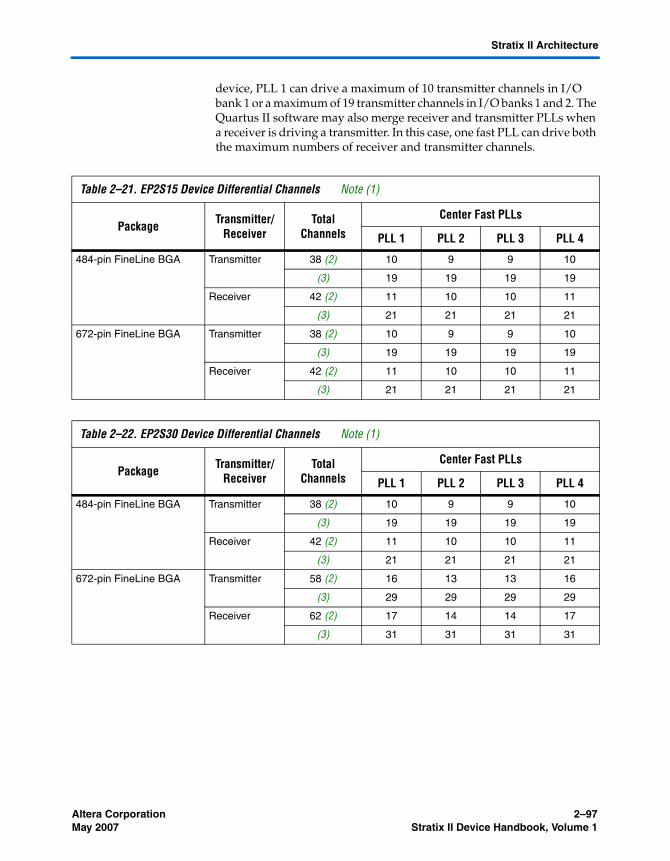
Altera Corporation 2–97May 2007 Stratix II Device Handbook, Volume 1
Stratix II Architecture
device, PLL 1 can drive a maximum of 10 transmitter channels in I/O bank 1 or a maximum of 19 transmitter channels in I/O banks 1 and 2. The Quartus II software may also merge receiver and transmitter PLLs when a receiver is driving a transmitter. In this case, one fast PLL can drive both the maximum numbers of receiver and transmitter channels.
Table 2–21. EP2S15 Device Differential Channels Note (1)
Package Transmitter/Receiver
Total Channels
Center Fast PLLs
PLL 1 PLL 2 PLL 3 PLL 4
484-pin FineLine BGA Transmitter 38 (2) 10 9 9 10
(3) 19 19 19 19
Receiver 42 (2) 11 10 10 11
(3) 21 21 21 21
672-pin FineLine BGA Transmitter 38 (2) 10 9 9 10
(3) 19 19 19 19
Receiver 42 (2) 11 10 10 11
(3) 21 21 21 21
Table 2–22. EP2S30 Device Differential Channels Note (1)
Package Transmitter/Receiver
Total Channels
Center Fast PLLs
PLL 1 PLL 2 PLL 3 PLL 4
484-pin FineLine BGA Transmitter 38 (2) 10 9 9 10
(3) 19 19 19 19
Receiver 42 (2) 11 10 10 11
(3) 21 21 21 21
672-pin FineLine BGA Transmitter 58 (2) 16 13 13 16
(3) 29 29 29 29
Receiver 62 (2) 17 14 14 17
(3) 31 31 31 31
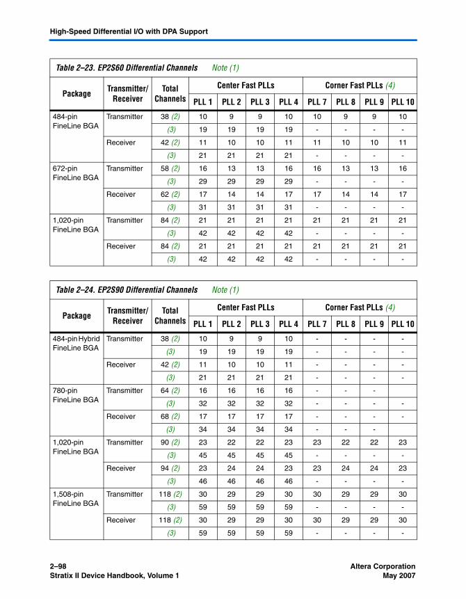
2–98 Altera CorporationStratix II Device Handbook, Volume 1 May 2007
High-Speed Differential I/O with DPA Support
Table 2–23. EP2S60 Differential Channels Note (1)
Package Transmitter/Receiver
Total Channels
Center Fast PLLs Corner Fast PLLs (4)
PLL 1 PLL 2 PLL 3 PLL 4 PLL 7 PLL 8 PLL 9 PLL 10
484-pin FineLine BGA
Transmitter 38 (2) 10 9 9 10 10 9 9 10
(3) 19 19 19 19 - - - -
Receiver 42 (2) 11 10 10 11 11 10 10 11
(3) 21 21 21 21 - - - -
672-pin FineLine BGA
Transmitter 58 (2) 16 13 13 16 16 13 13 16
(3) 29 29 29 29 - - - -
Receiver 62 (2) 17 14 14 17 17 14 14 17
(3) 31 31 31 31 - - - -
1,020-pin FineLine BGA
Transmitter 84 (2) 21 21 21 21 21 21 21 21
(3) 42 42 42 42 - - - -
Receiver 84 (2) 21 21 21 21 21 21 21 21
(3) 42 42 42 42 - - - -
Table 2–24. EP2S90 Differential Channels Note (1)
Package Transmitter/Receiver
Total Channels
Center Fast PLLs Corner Fast PLLs (4)
PLL 1 PLL 2 PLL 3 PLL 4 PLL 7 PLL 8 PLL 9 PLL 10
484-pin Hybrid FineLine BGA
Transmitter 38 (2) 10 9 9 10 - - - -
(3) 19 19 19 19 - - - -
Receiver 42 (2) 11 10 10 11 - - - -
(3) 21 21 21 21 - - - -
780-pin FineLine BGA
Transmitter 64 (2) 16 16 16 16 - - -
(3) 32 32 32 32 - - - -
Receiver 68 (2) 17 17 17 17 - - - -
(3) 34 34 34 34 - - -
1,020-pin FineLine BGA
Transmitter 90 (2) 23 22 22 23 23 22 22 23
(3) 45 45 45 45 - - - -
Receiver 94 (2) 23 24 24 23 23 24 24 23
(3) 46 46 46 46 - - - -
1,508-pin FineLine BGA
Transmitter 118 (2) 30 29 29 30 30 29 29 30
(3) 59 59 59 59 - - - -
Receiver 118 (2) 30 29 29 30 30 29 29 30
(3) 59 59 59 59 - - - -
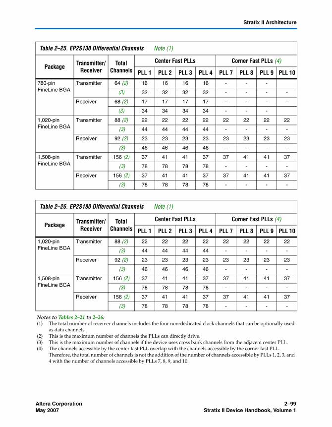
Altera Corporation 2–99May 2007 Stratix II Device Handbook, Volume 1
Stratix II Architecture
Table 2–25. EP2S130 Differential Channels Note (1)
Package Transmitter/Receiver
Total Channels
Center Fast PLLs Corner Fast PLLs (4)
PLL 1 PLL 2 PLL 3 PLL 4 PLL 7 PLL 8 PLL 9 PLL 10
780-pin FineLine BGA
Transmitter 64 (2) 16 16 16 16 - - -
(3) 32 32 32 32 - - - -
Receiver 68 (2) 17 17 17 17 - - - -
(3) 34 34 34 34 - - -
1,020-pin FineLine BGA
Transmitter 88 (2) 22 22 22 22 22 22 22 22
(3) 44 44 44 44 - - - -
Receiver 92 (2) 23 23 23 23 23 23 23 23
(3) 46 46 46 46 - - - -
1,508-pin FineLine BGA
Transmitter 156 (2) 37 41 41 37 37 41 41 37
(3) 78 78 78 78 - - - -
Receiver 156 (2) 37 41 41 37 37 41 41 37
(3) 78 78 78 78 - - - -
Table 2–26. EP2S180 Differential Channels Note (1)
Package Transmitter/Receiver
Total Channels
Center Fast PLLs Corner Fast PLLs (4)
PLL 1 PLL 2 PLL 3 PLL 4 PLL 7 PLL 8 PLL 9 PLL 10
1,020-pin FineLine BGA
Transmitter 88 (2) 22 22 22 22 22 22 22 22
(3) 44 44 44 44 - - - -
Receiver 92 (2) 23 23 23 23 23 23 23 23
(3) 46 46 46 46 - - - -
1,508-pin FineLine BGA
Transmitter 156 (2) 37 41 41 37 37 41 41 37
(3) 78 78 78 78 - - - -
Receiver 156 (2) 37 41 41 37 37 41 41 37
(3) 78 78 78 78 - - - -
Notes to Tables 2–21 to 2–26:(1) The total number of receiver channels includes the four non-dedicated clock channels that can be optionally used
as data channels.(2) This is the maximum number of channels the PLLs can directly drive.(3) This is the maximum number of channels if the device uses cross bank channels from the adjacent center PLL.(4) The channels accessible by the center fast PLL overlap with the channels accessible by the corner fast PLL.
Therefore, the total number of channels is not the addition of the number of channels accessible by PLLs 1, 2, 3, and 4 with the number of channels accessible by PLLs 7, 8, 9, and 10.
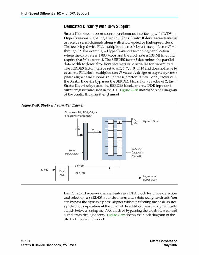
2–100 Altera CorporationStratix II Device Handbook, Volume 1 May 2007
High-Speed Differential I/O with DPA Support
Dedicated Circuitry with DPA Support
Stratix II devices support source-synchronous interfacing with LVDS or HyperTransport signaling at up to 1 Gbps. Stratix II devices can transmit or receive serial channels along with a low-speed or high-speed clock. The receiving device PLL multiplies the clock by an integer factor W = 1 through 32. For example, a HyperTransport technology application where the data rate is 1,000 Mbps and the clock rate is 500 MHz would require that W be set to 2. The SERDES factor J determines the parallel data width to deserialize from receivers or to serialize for transmitters. The SERDES factor J can be set to 4, 5, 6, 7, 8, 9, or 10 and does not have to equal the PLL clock-multiplication W value. A design using the dynamic phase aligner also supports all of these J factor values. For a J factor of 1, the Stratix II device bypasses the SERDES block. For a J factor of 2, the Stratix II device bypasses the SERDES block, and the DDR input and output registers are used in the IOE. Figure 2–58 shows the block diagram of the Stratix II transmitter channel.
Figure 2–58. Stratix II Transmitter Channel
Each Stratix II receiver channel features a DPA block for phase detection and selection, a SERDES, a synchronizer, and a data realigner circuit. You can bypass the dynamic phase aligner without affecting the basic source-synchronous operation of the channel. In addition, you can dynamically switch between using the DPA block or bypassing the block via a control signal from the logic array. Figure 2–59 shows the block diagram of the Stratix II receiver channel.
FastPLL
refclk
diffioclk
DedicatedTransmitterInterface
LocalInterconnect
10
+–
Up to 1 Gbps
load_enRegional orglobal clock
Data from R4, R24, C4, ordirect link interconnect
10
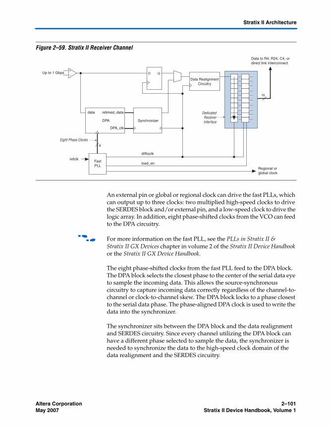
Altera Corporation 2–101May 2007 Stratix II Device Handbook, Volume 1
Stratix II Architecture
Figure 2–59. Stratix II Receiver Channel
An external pin or global or regional clock can drive the fast PLLs, which can output up to three clocks: two multiplied high-speed clocks to drive the SERDES block and/or external pin, and a low-speed clock to drive the logic array. In addition, eight phase-shifted clocks from the VCO can feed to the DPA circuitry.
f For more information on the fast PLL, see the PLLs in Stratix II & Stratix II GX Devices chapter in volume 2 of the Stratix II Device Handbook or the Stratix II GX Device Handbook.
The eight phase-shifted clocks from the fast PLL feed to the DPA block. The DPA block selects the closest phase to the center of the serial data eye to sample the incoming data. This allows the source-synchronous circuitry to capture incoming data correctly regardless of the channel-to-channel or clock-to-channel skew. The DPA block locks to a phase closest to the serial data phase. The phase-aligned DPA clock is used to write the data into the synchronizer.
The synchronizer sits between the DPA block and the data realignment and SERDES circuitry. Since every channel utilizing the DPA block can have a different phase selected to sample the data, the synchronizer is needed to synchronize the data to the high-speed clock domain of the data realignment and the SERDES circuitry.
+–
FastPLL
refclkload_en
diffioclk
Regional orglobal clock
Data to R4, R24, C4, ordirect link interconnect
Up to 1 Gbps
10
DedicatedReceiverInterface
Eight Phase Clocks
data retimed_data
DPA_clk
DPA Synchronizer
8
D Q
Data RealignmentCircuitry
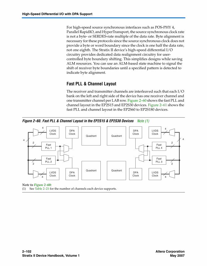
2–102 Altera CorporationStratix II Device Handbook, Volume 1 May 2007
High-Speed Differential I/O with DPA Support
For high-speed source synchronous interfaces such as POS-PHY 4, Parallel RapidIO, and HyperTransport, the source synchronous clock rate is not a byte- or SERDES-rate multiple of the data rate. Byte alignment is necessary for these protocols since the source synchronous clock does not provide a byte or word boundary since the clock is one half the data rate, not one eighth. The Stratix II device’s high-speed differential I/O circuitry provides dedicated data realignment circuitry for user-controlled byte boundary shifting. This simplifies designs while saving ALM resources. You can use an ALM-based state machine to signal the shift of receiver byte boundaries until a specified pattern is detected to indicate byte alignment.
Fast PLL & Channel Layout
The receiver and transmitter channels are interleaved such that each I/O bank on the left and right side of the device has one receiver channel and one transmitter channel per LAB row. Figure 2–60 shows the fast PLL and channel layout in the EP2S15 and EP2S30 devices. Figure 2–61 shows the fast PLL and channel layout in the EP2S60 to EP2S180 devices.
Figure 2–60. Fast PLL & Channel Layout in the EP2S15 & EP2S30 Devices Note (1)
Note to Figure 2–60:(1) See Table 2–21 for the number of channels each device supports.
LVDSClock
DPAClock
FastPLL 1
FastPLL 2
LVDSClock
DPAClock
LVDSClock
DPAClock
FastPLL 4
FastPLL 3
LVDSClock
DPAClock
Quadrant
Quadrant
Quadrant
Quadrant
4
4
4 4
4
42
2
2
2
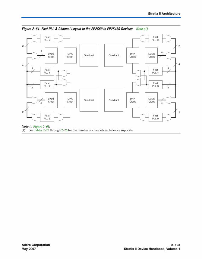
Altera Corporation 2–103May 2007 Stratix II Device Handbook, Volume 1
Stratix II Architecture
Figure 2–61. Fast PLL & Channel Layout in the EP2S60 to EP2S180 Devices Note (1)
Note to Figure 2–61:(1) See Tables 2–22 through 2–26 for the number of channels each device supports.
LVDSClock
DPAClock
FastPLL 1
FastPLL 2
LVDSClock
DPAClock
LVDSClock
DPAClock
FastPLL 4
FastPLL 7
FastPLL 10
FastPLL 3
LVDSClock
DPAClock
Quadrant
Quadrant
Quadrant
Quadrant
4
4
2
4 4
4
4
2
2
2
2
2
FastPLL 8
FastPLL 9
2 2
2–104 Altera CorporationStratix II Device Handbook, Volume 1 May 2007
Document Revision History
Document Revision History
Table 2–27 shows the revision history for this chapter.
Table 2–27. Document Revision History (Part 1 of 2)
Date and Document Version
Changes Made Summary of Changes
May 2007, v4.3 Updated “Clock Control Block” section. —
Updated note in the “Clock Control Block” section. —
Deleted Tables 2-11 and 2-12. —
Updated notes to:● Figure 2–41● Figure 2–42● Figure 2–43● Figure 2–45
—
Updated notes to Table 2–18. —
Moved Document Revision History to end of the chapter. —
August 2006, v4.2
Updated Table 2–18 with note. —
April 2006, v4.1
● Updated Table 2–13.● Removed Note 2 from Table 2–16.● Updated “On-Chip Termination” section and Table 2–19 to
include parallel termination with calibration information.● Added new “On-Chip Parallel Termination with Calibration”
section.● Updated Figure 2–44.
● Added parallel on-chip termination description and specification.
● Changed RCLK names to match the Quartus II software in Table 2–13.
December 2005, v4.0
Updated “Clock Control Block” section. —
July 2005, v3.1 ● Updated HyperTransport technology information in Table 2–18.● Updated HyperTransport technology information in
Figure 2–57.● Added information on the asynchronous clear signal.
—
May 2005, v3.0 ● Updated “Functional Description” section.● Updated Table 2–3.● Updated “Clock Control Block” section.● Updated Tables 2–17 through 2–19.● Updated Tables 2–20 through 2–22.● Updated Figure 2–57.
—
March 2005, 2.1
● Updated “Functional Description” section.● Updated Table 2–3.
—
Altera Corporation 2–105May 2007 Stratix II Device Handbook, Volume 1
Stratix II Architecture
January 2005, v2.0
● Updated the “MultiVolt I/O Interface” and “TriMatrix Memory” sections.
● Updated Tables 2–3, 2–17, and 2–19.
—
October 2004, v1.2
● Updated Tables 2–9, 2–16, 2–26, and 2–27. —
July 2004, v1.1 ● Updated note to Tables 2–9 and 2–16.● Updated Tables 2–16, 2–17, 2–18, 2–19, and 2–20.● Updated Figures 2–41, 2–42, and 2–57.● Removed 3 from list of SERDES factor J.● Updated “High-Speed Differential I/O with DPA Support”
section.● In “Dedicated Circuitry with DPA Support” section, removed
XSBI and changed RapidIO to Parallel RapidIO.
—
February 2004, v1.0
Added document to the Stratix II Device Handbook. —
Table 2–27. Document Revision History (Part 2 of 2)
Date and Document Version
Changes Made Summary of Changes

2–106 Altera CorporationStratix II Device Handbook, Volume 1 May 2007
Document Revision History