Embed Size (px)
Citation preview
Altera Corporation Section I–1
Section I. Stratix II DeviceFamily Data Sheet
This section provides the data sheet specifications for Stratix® II devices. This section contains feature definitions of the internal architecture, configuration and JTAG boundary-scan testing information, DC operating conditions, AC timing parameters, a reference to power consumption, and ordering information for Stratix II devices.
This section contains the following chapters:
■ Chapter 1, Introduction
■ Chapter 2, Stratix II Architecture
■ Chapter 3, Configuration & Testing
■ Chapter 4, Hot Socketing & Power-On Reset
■ Chapter 5, DC & Switching Characteristics
■ Chapter 6, Reference & Ordering Information
Section I–2 Altera Corporation
Stratix II Device Family Data Sheet Stratix II Device Handbook, Volume 1
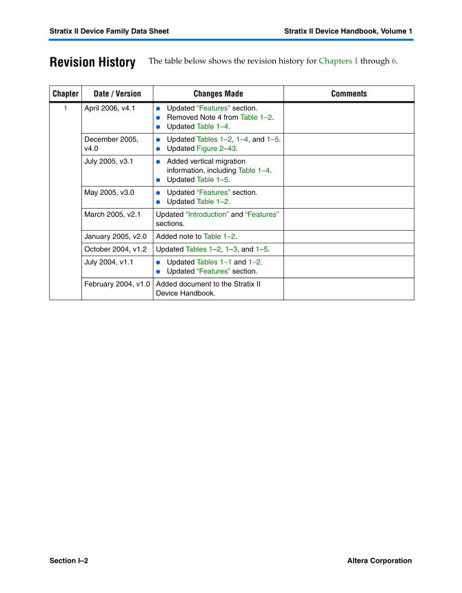
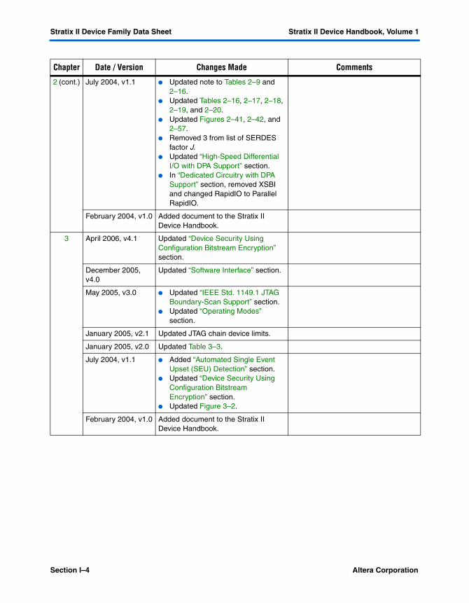
Revision History The table below shows the revision history for Chapters 1 through 6.
Chapter Date / Version Changes Made Comments
1 April 2006, v4.1 ● Updated “Features” section.● Removed Note 4 from Table 1–2.● Updated Table 1–4.
December 2005, v4.0
● Updated Tables 1–2, 1–4, and 1–5.● Updated Figure 2–43.
July 2005, v3.1 ● Added vertical migration information, including Table 1–4.
● Updated Table 1–5.
May 2005, v3.0 ● Updated “Features” section.● Updated Table 1–2.
March 2005, v2.1 Updated “Introduction” and “Features” sections.
January 2005, v2.0 Added note to Table 1–2.
October 2004, v1.2 Updated Tables 1–2, 1–3, and 1–5.
July 2004, v1.1 ● Updated Tables 1–1 and 1–2.● Updated “Features” section.
February 2004, v1.0 Added document to the Stratix II Device Handbook.
Section I–3 Altera Corporation
Stratix II Device Family Data Sheet Stratix II Device Handbook, Volume 1
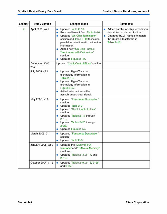
2 April 2006, v4.1 ● Updated Table 2–13.● Removed Note 2 from Table 2–16.● Updated “On-Chip Termination”
section and Table 2–19 to include parallel termination with calibration information.
● Added new “On-Chip Parallel Termination with Calibration” section.
● Updated Figure 2–44.
● Added parallel on-chip termination description and specification.
● Changed RCLK names to match the Quartus II software in Table 2–13.
December 2005, v4.0
Updated “Clock Control Block” section.
July 2005, v3.1 ● Updated HyperTransport technology information in Table 2–18.
● Updated HyperTransport technology information in Figure 2–57.
● Added information on the asynchronous clear signal.
May 2005, v3.0 ● Updated “Functional Description” section.
● Updated Table 2–3.● Updated “Clock Control Block”
section.● Updated Tables 2–17 through
2–19.● Updated Tables 2–20 through
2–22.● Updated Figure 2–57.
March 2005, 2.1 ● Updated “Functional Description” section.
● Updated Table 2–3.
January 2005, v2.0 ● Updated the “MultiVolt I/O Interface” and “TriMatrix Memory” sections.
● Updated Tables 2–3, 2–17, and 2–19.
October 2004, v1.2 ● Updated Tables 2–9, 2–16, 2–26, and 2–27.
Chapter Date / Version Changes Made Comments
Section I–4 Altera Corporation
Stratix II Device Family Data Sheet Stratix II Device Handbook, Volume 1
2 (cont.) July 2004, v1.1 ● Updated note to Tables 2–9 and 2–16.
● Updated Tables 2–16, 2–17, 2–18, 2–19, and 2–20.
● Updated Figures 2–41, 2–42, and 2–57.
● Removed 3 from list of SERDES factor J.
● Updated “High-Speed Differential I/O with DPA Support” section.
● In “Dedicated Circuitry with DPA Support” section, removed XSBI and changed RapidIO to Parallel RapidIO.
February 2004, v1.0 Added document to the Stratix II Device Handbook.
3 April 2006, v4.1 Updated “Device Security Using Configuration Bitstream Encryption” section.
December 2005, v4.0
Updated “Software Interface” section.
May 2005, v3.0 ● Updated “IEEE Std. 1149.1 JTAG Boundary-Scan Support” section.
● Updated “Operating Modes” section.
January 2005, v2.1 Updated JTAG chain device limits.
January 2005, v2.0 Updated Table 3–3.
July 2004, v1.1 ● Added “Automated Single Event Upset (SEU) Detection” section.
● Updated “Device Security Using Configuration Bitstream Encryption” section.
● Updated Figure 3–2.
February 2004, v1.0 Added document to the Stratix II Device Handbook.
Chapter Date / Version Changes Made Comments
Altera Corporation I–5
Stratix II Device Family Data Sheet
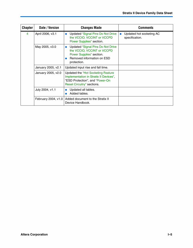
4 April 2006, v3.1 ● Updated “Signal Pins Do Not Drive the VCCIO, VCCINT or VCCPD Power Supplies” section.
● Updated hot socketing AC specification.
May 2005, v3.0 ● Updated “Signal Pins Do Not Drive the VCCIO, VCCINT or VCCPD Power Supplies” section.
● Removed information on ESD protection.
January 2005, v2.1 Updated input rise and fall time.
January 2005, v2.0 Updated the “Hot Socketing Feature Implementation in Stratix II Devices”, “ESD Protection”, and “Power-On Reset Circuitry” sections.
July 2004, v1.1 ● Updated all tables.● Added tables.
February 2004, v1.0 Added document to the Stratix II Device Handbook.
Chapter Date / Version Changes Made Comments
I–6 Altera Corporation
Stratix II Device Family Data Sheet Stratix II Device Handbook, Volume 1
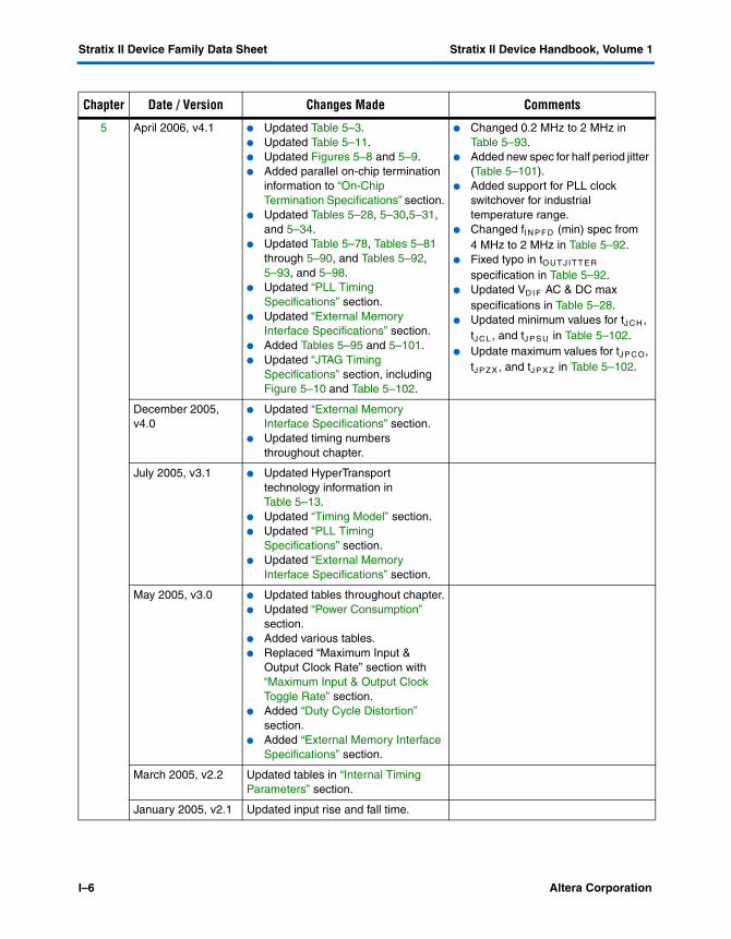
5 April 2006, v4.1 ● Updated Table 5–3.● Updated Table 5–11.● Updated Figures 5–8 and 5–9.● Added parallel on-chip termination
information to “On-Chip Termination Specifications” section.
● Updated Tables 5–28, 5–30,5–31, and 5–34.
● Updated Table 5–78, Tables 5–81 through 5–90, and Tables 5–92, 5–93, and 5–98.
● Updated “PLL Timing Specifications” section.
● Updated “External Memory Interface Specifications” section.
● Added Tables 5–95 and 5–101.● Updated “JTAG Timing
Specifications” section, including Figure 5–10 and Table 5–102.
● Changed 0.2 MHz to 2 MHz in Table 5–93.
● Added new spec for half period jitter (Table 5–101).
● Added support for PLL clock switchover for industrial temperature range.
● Changed fI N P F D (min) spec from 4 MHz to 2 MHz in Table 5–92.
● Fixed typo in tO UT J I T T E R specification in Table 5–92.
● Updated VD I F AC & DC max specifications in Table 5–28.
● Updated minimum values for tJ CH, tJ C L, and tJ P S U in Table 5–102.
● Update maximum values for tJ P C O, tJ P Z X, and tJ P X Z in Table 5–102.
December 2005, v4.0
● Updated “External Memory Interface Specifications” section.
● Updated timing numbers throughout chapter.
July 2005, v3.1 ● Updated HyperTransport technology information in Table 5–13.
● Updated “Timing Model” section.● Updated “PLL Timing
Specifications” section.● Updated “External Memory
Interface Specifications” section.
May 2005, v3.0 ● Updated tables throughout chapter.● Updated “Power Consumption”
section.● Added various tables.● Replaced “Maximum Input &
Output Clock Rate” section with “Maximum Input & Output Clock Toggle Rate” section.
● Added “Duty Cycle Distortion” section.
● Added “External Memory Interface Specifications” section.
March 2005, v2.2 Updated tables in “Internal Timing Parameters” section.
January 2005, v2.1 Updated input rise and fall time.
Chapter Date / Version Changes Made Comments
Altera Corporation I–7
Stratix II Device Family Data Sheet
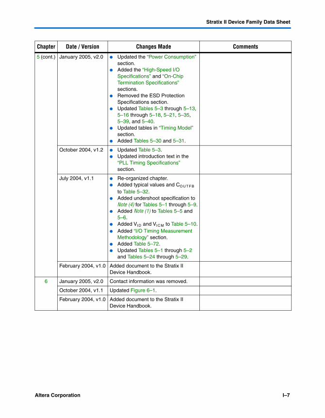
5 (cont.) January 2005, v2.0 ● Updated the “Power Consumption” section.
● Added the “High-Speed I/O Specifications” and “On-Chip Termination Specifications” sections.
● Removed the ESD Protection Specifications section.
● Updated Tables 5–3 through 5–13, 5–16 through 5–18, 5–21, 5–35, 5–39, and 5–40.
● Updated tables in “Timing Model” section.
● Added Tables 5–30 and 5–31.
October 2004, v1.2 ● Updated Table 5–3.● Updated introduction text in the
“PLL Timing Specifications” section.
July 2004, v1.1 ● Re-organized chapter.● Added typical values and CO UT F B
to Table 5–32.● Added undershoot specification to
Note (4) for Tables 5–1 through 5–9.● Added Note (1) to Tables 5–5 and
5–6.● Added VI D and VI C M to Table 5–10.● Added “I/O Timing Measurement
Methodology” section.● Added Table 5–72.● Updated Tables 5–1 through 5–2
and Tables 5–24 through 5–29.
February 2004, v1.0 Added document to the Stratix II Device Handbook.
6 January 2005, v2.0 Contact information was removed.
October 2004, v1.1 Updated Figure 6–1.
February 2004, v1.0 Added document to the Stratix II Device Handbook.
Chapter Date / Version Changes Made Comments

I–8 Altera Corporation
Stratix II Device Family Data Sheet Stratix II Device Handbook, Volume 1
Altera Corporation 1–1April 2006
1. Introduction
Introduction The Stratix® II FPGA family is based on a 1.2-V, 90-nm, all-layer copper SRAM process and features a new logic structure that maximizes performance, and enables device densities approaching 180,000 equivalent logic elements (LEs). Stratix II devices offer up to 9 Mbits of on-chip, TriMatrix™ memory for demanding, memory intensive applications and has up to 96 DSP blocks with up to 384 (18-bit × 18-bit) multipliers for efficient implementation of high performance filters and other DSP functions. Various high-speed external memory interfaces are supported, including double data rate (DDR) SDRAM and DDR2 SDRAM, RLDRAM II, quad data rate (QDR) II SRAM, and single data rate (SDR) SDRAM. Stratix II devices support various I/O standards along with support for 1-gigabit per second (Gbps) source synchronous signaling with DPA circuitry. Stratix II devices offer a complete clock management solution with internal clock frequency of up to 550 MHz and up to 12 phase-locked loops (PLLs). Stratix II devices are also the industry’s first FPGAs with the ability to decrypt a configuration bitstream using the Advanced Encryption Standard (AES) algorithm to protect designs.
Features The Stratix II family offers the following features:
■ 15,600 to 179,400 equivalent LEs; see Table 1–1■ New and innovative adaptive logic module (ALM), the basic
building block of the Stratix II architecture, maximizes performance and resource usage efficiency
■ Up to 9,383,040 RAM bits (1,172,880 bytes) available without reducing logic resources
■ TriMatrix memory consisting of three RAM block sizes to implement true dual-port memory and first-in first-out (FIFO) buffers
■ High-speed DSP blocks provide dedicated implementation of multipliers (at up to 450 MHz), multiply-accumulate functions, and finite impulse response (FIR) filters
■ Up to 16 global clocks with 24 clocking resources per device region■ Clock control blocks support dynamic clock network
enable/disable, which allows clock networks to power down to reduce power consumption in user mode
■ Up to 12 PLLs (four enhanced PLLs and eight fast PLLs) per device provide spread spectrum, programmable bandwidth, clock switch-over, real-time PLL reconfiguration, and advanced multiplication and phase shifting
SII51001-4.1
1–2 Altera CorporationStratix II Device Handbook, Volume 1 April 2006
Features
■ Support for numerous single-ended and differential I/O standards■ High-speed differential I/O support with DPA circuitry for 1-Gbps
performance■ Support for high-speed networking and communications bus
standards including Parallel RapidIO, SPI-4 Phase 2 (POS-PHY Level 4), HyperTransport™ technology, and SFI-4
■ Support for high-speed external memory, including DDR and DDR2 SDRAM, RLDRAM II, QDR II SRAM, and SDR SDRAM
■ Support for multiple intellectual property megafunctions from Altera MegaCore® functions and Altera Megafunction Partners Program (AMPPSM) megafunctions
■ Support for design security using configuration bitstream encryption
■ Support for remote configuration updates
Table 1–1. Stratix II FPGA Family Features
Feature EP2S15 EP2S30 EP2S60 EP2S90 EP2S130 EP2S180
ALMs 6,240 13,552 24,176 36,384 53,016 71,760
Adaptive look-up tables (ALUTs) (1) 12,480 27,104 48,352 72,768 106,032 143,520
Equivalent LEs (2) 15,600 33,880 60,440 90,960 132,540 179,400
M512 RAM blocks 104 202 329 488 699 930
M4K RAM blocks 78 144 255 408 609 768
M-RAM blocks 0 1 2 4 6 9
Total RAM bits 419,328 1,369,728 2,544,192 4,520,488 6,747,840 9,383,040
DSP blocks 12 16 36 48 63 96
18-bit × 18-bit multipliers (3) 48 64 144 192 252 384
Enhanced PLLs 2 2 4 4 4 4
Fast PLLs 4 4 8 8 8 8
Maximum user I/O pins 366 500 718 902 1,126 1,170
Notes to Table 1–1:(1) One ALM contains two ALUTs. The ALUT is the cell used in the Quartus® II software for logic synthesis.(2) This is the equivalent number of LEs in a Stratix device (four-input LUT-based architecture).(3) These multipliers are implemented using the DSP blocks.
Altera Corporation 1–3April 2006 Stratix II Device Handbook, Volume 1
Introduction
Stratix II devices are available in space-saving FineLine BGA® packages (see Tables 1–2 and 1–3).
All Stratix II devices support vertical migration within the same package (for example, you can migrate between the EP2S15, EP2S30, and EP2S60 devices in the 672-pin FineLine BGA package). Vertical migration means that you can migrate to devices whose dedicated pins, configuration pins, and power pins are the same for a given package across device densities.
To ensure that a board layout supports migratable densities within one package offering, enable the applicable vertical migration path within the Quartus II software (Assignments menu > Device > Migration Devices).
Table 1–2. Stratix II Package Options & I/O Pin Counts Notes (1), (2)
Device 484-Pin FineLine BGA
484-Pin Hybrid
FineLine BGA
672-Pin FineLine
BGA
780-Pin FineLine
BGA
1,020-Pin FineLine BGA
1,508-Pin FineLine BGA
EP2S15 342 366
EP2S30 342 500
EP2S60 (3) 334 492 718
EP2S90 (3) 308 534 758 902
EP2S130 (3) 534 742 1,126
EP2S180 (3) 742 1,170
Notes to Table 1–2:(1) All I/O pin counts include eight dedicated clock input pins (clk1p, clk1n, clk3p, clk3n, clk9p, clk9n,
clk11p, and clk11n) that can be used for data inputs.(2) The Quartus II software I/O pin counts include one additional pin, PLL_ENA, which is not available as general-
purpose I/O pins. The PLL_ENA pin can only be used to enable the PLLs within the device.(3) The I/O pin counts for the EP2S60, EP2S90, EP2S130, and EP2S180 devices in the 1020-pin and 1508-pin packages
include eight dedicated fast PLL clock inputs (FPLL7CLKp/n, FPLL8CLKp/n, FPLL9CLKp/n, and FPLL10CLKp/n) that can be used for data inputs.
Table 1–3. Stratix II FineLine BGA Package Sizes
Dimension 484 Pin 484-Pin Hybrid 672 Pin 780 Pin 1,020 Pin 1,508 Pin
Pitch (mm) 1.00 1.00 1.00 1.00 1.00 1.00
Area (mm2) 529 729 729 841 1,089 1,600
Length × width (mm × mm)
23 × 23 27 × 27 27 × 27 29 × 29 33 × 33 40 × 40
1–4 Altera CorporationStratix II Device Handbook, Volume 1 April 2006
Features
After compilation, check the information messages for a full list of I/O, DQ, LVDS, and other pins that are not available because of the selected migration path.
Table 1–4 lists the Stratix II device package offerings and shows the total number of non-migratable user I/O pins when migrating from one density device to a larger density device. Additional I/O pins may not be migratable if migrating from the larger device to the smaller density device.
1 When moving from one density to a larger density, the larger density device may have fewer user I/O pins. The larger device requires more power and ground pins to support the additional logic within the device. Use the Quartus II Pin Planner to determine which user I/O pins are migratable between the two devices.
1 To determine if your user I/O assignments are correct, run the I/O Assignment Analysis command in the Quartus II software (Processing > Start > Start I/O Assignment Analysis).
f Refer to the I/O Management chapter in volume 2 of the Quartus II Handbook for more information on pin migration.
Table 1–4. Total Number of Non-Migratable I/O Pins for Stratix II Vertical Migration Paths
Vertical Migration Path
484-Pin FineLine BGA
672-Pin FineLine BGA
780-Pin FineLine BGA
1020-Pin FineLine BGA
1508-Pin FineLine BGA
EP2S15 to EP2S30 0 (1) 0
EP2S15 to EP2S60 8 (1) 0
EP2S30 to EP2S60 8 (1) 8
EP2S60 to EP2S90 0
EP2S60 to EP2S130 0
EP2S60 to EP2S180 0
EP2S90 to EP2S130 0 (1) 16 17
EP2S90 to EP2S180 16 0
EP2S130 to EP2S180 0 0
Note to Table 1–4:(1) Some of the DQ/DQS pins are not migratable. Refer to the Quartus II software information messages for more
detailed information.
Altera Corporation 1–5April 2006 Stratix II Device Handbook, Volume 1
Introduction
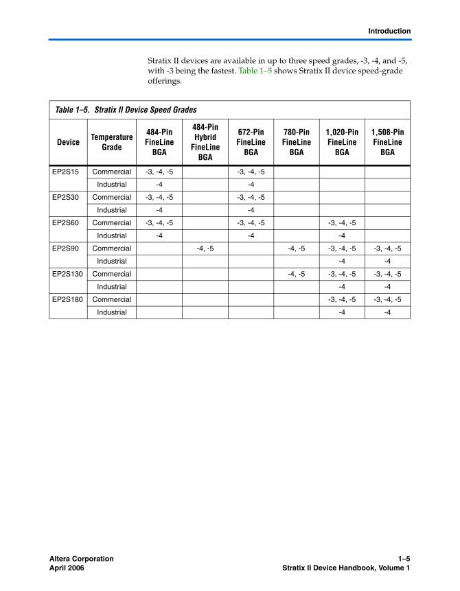
Stratix II devices are available in up to three speed grades, -3, -4, and -5, with -3 being the fastest. Table 1–5 shows Stratix II device speed-grade offerings.
Table 1–5. Stratix II Device Speed Grades
Device Temperature Grade
484-Pin FineLine
BGA
484-Pin Hybrid
FineLine BGA
672-Pin FineLine
BGA
780-Pin FineLine
BGA
1,020-Pin FineLine
BGA
1,508-Pin FineLine
BGA
EP2S15 Commercial -3, -4, -5 -3, -4, -5
Industrial -4 -4
EP2S30 Commercial -3, -4, -5 -3, -4, -5
Industrial -4 -4
EP2S60 Commercial -3, -4, -5 -3, -4, -5 -3, -4, -5
Industrial -4 -4 -4
EP2S90 Commercial -4, -5 -4, -5 -3, -4, -5 -3, -4, -5
Industrial -4 -4
EP2S130 Commercial -4, -5 -3, -4, -5 -3, -4, -5
Industrial -4 -4
EP2S180 Commercial -3, -4, -5 -3, -4, -5
Industrial -4 -4
1–6 Altera CorporationStratix II Device Handbook, Volume 1 April 2006
Features
Altera Corporation 2–1April 2006
2. Stratix II Architecture
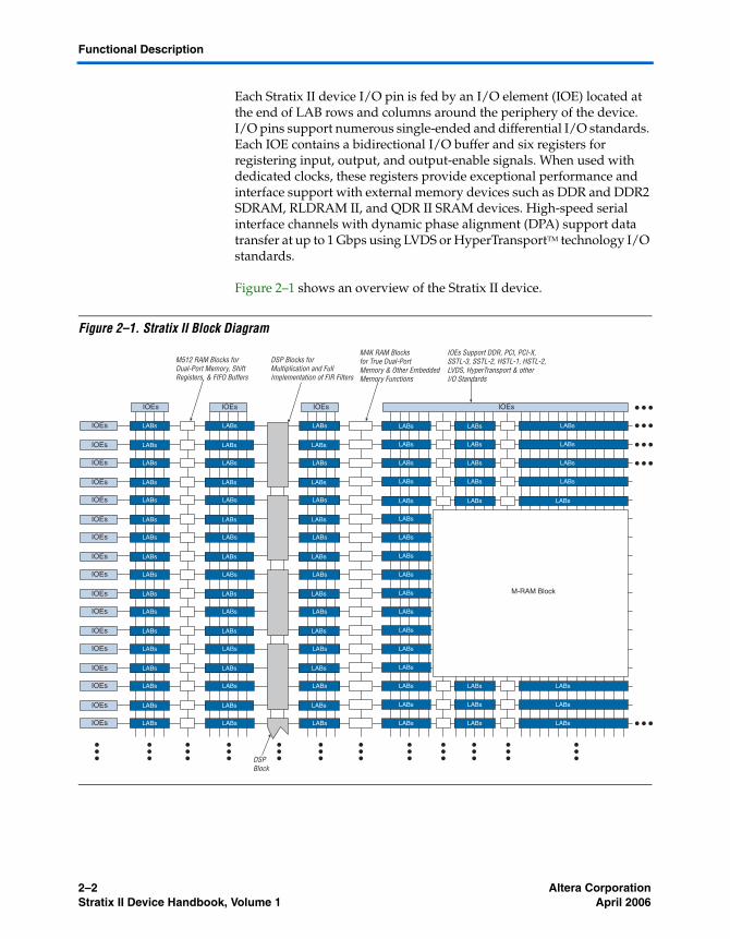
Functional Description
Stratix® II devices contain a two-dimensional row- and column-based architecture to implement custom logic. A series of column and row interconnects of varying length and speed provides signal interconnects between logic array blocks (LABs), memory block structures (M512 RAM, M4K RAM, and M-RAM blocks), and digital signal processing (DSP) blocks.
Each LAB consists of eight adaptive logic modules (ALMs). An ALM is the Stratix II device family’s basic building block of logic providing efficient implementation of user logic functions. LABs are grouped into rows and columns across the device.
M512 RAM blocks are simple dual-port memory blocks with 512 bits plus parity (576 bits). These blocks provide dedicated simple dual-port or single-port memory up to 18-bits wide at up to 500 MHz. M512 blocks are grouped into columns across the device in between certain LABs.
M4K RAM blocks are true dual-port memory blocks with 4K bits plus parity (4,608 bits). These blocks provide dedicated true dual-port, simple dual-port, or single-port memory up to 36-bits wide at up to 550 MHz. These blocks are grouped into columns across the device in between certain LABs.
M-RAM blocks are true dual-port memory blocks with 512K bits plus parity (589,824 bits). These blocks provide dedicated true dual-port, simple dual-port, or single-port memory up to 144-bits wide at up to 420 MHz. Several M-RAM blocks are located individually in the device's logic array.
DSP blocks can implement up to either eight full-precision 9 × 9-bit multipliers, four full-precision 18 × 18-bit multipliers, or one full-precision 36 × 36-bit multiplier with add or subtract features. The DSP blocks support Q1.15 format rounding and saturation in the multiplier and accumulator stages. These blocks also contain shift registers for digital signal processing applications, including finite impulse response (FIR) and infinite impulse response (IIR) filters. DSP blocks are grouped into columns across the device and operate at up to 450 MHz.
SII51002-4.1
2–2 Altera CorporationStratix II Device Handbook, Volume 1 April 2006
Functional Description
Each Stratix II device I/O pin is fed by an I/O element (IOE) located at the end of LAB rows and columns around the periphery of the device. I/O pins support numerous single-ended and differential I/O standards. Each IOE contains a bidirectional I/O buffer and six registers for registering input, output, and output-enable signals. When used with dedicated clocks, these registers provide exceptional performance and interface support with external memory devices such as DDR and DDR2 SDRAM, RLDRAM II, and QDR II SRAM devices. High-speed serial interface channels with dynamic phase alignment (DPA) support data transfer at up to 1 Gbps using LVDS or HyperTransportTM technology I/O standards.
Figure 2–1 shows an overview of the Stratix II device.
Figure 2–1. Stratix II Block Diagram
M512 RAM Blocks for Dual-Port Memory, Shift Registers, & FIFO Buffers
DSP Blocks forMultiplication and FullImplementation of FIR Filters
M4K RAM Blocksfor True Dual-Port Memory & Other EmbeddedMemory Functions
IOEs Support DDR, PCI, PCI-X, SSTL-3, SSTL-2, HSTL-1, HSTL-2, LVDS, HyperTransport & otherI/O Standards
IOEs
IOEs
IOEs
IOEs
IOEs
IOEs
IOEs
IOEs
IOEs
IOEs
IOEs
IOEs
IOEs
IOEs
IOEs
IOEs
IOEs
LABs
LABs
IOEs
LABs
LABs
LABs
LABs
LABs
LABs
LABs
LABs
LABs
LABs
LABs
LABs
LABs
LABs
LABs
LABs
LABs
IOEs
LABs
LABs
LABs
LABs
LABs
LABs
LABs
LABs
LABs
LABs
LABs
LABs
LABs
LABs
LABs
LABs LABs
LABs
IOEs IOEs
LABs
LABs LABs
LABs LABs
LABs
LABs
LABs
LABs
LABs
LABs
LABs
LABs
LABs
LABs
LABs
LABs
LABs
LABs
LABs LABs
LABs
LABs
LABs
LABs
LABs
LABs
LABs
LABs
LABs
LABs
LABs
LABsLABs
LABsLABs
LABsLABs
LABs
LABs
LABs
LABs
LABs
LABs
LABs
LABs
LABs
DSPBlock
M-RAM Block
Altera Corporation 2–3April 2006 Stratix II Device Handbook, Volume 1
Stratix II Architecture
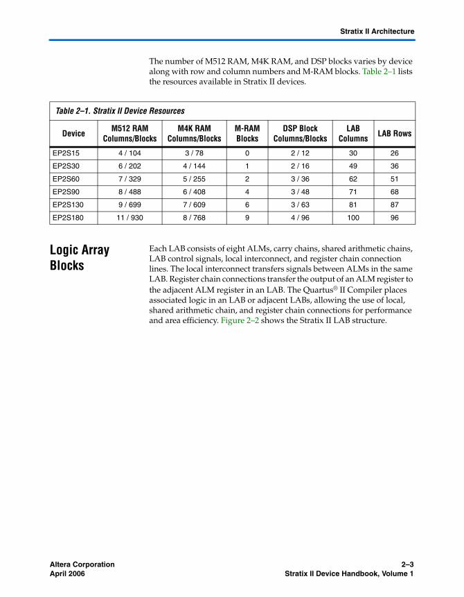
The number of M512 RAM, M4K RAM, and DSP blocks varies by device along with row and column numbers and M-RAM blocks. Table 2–1 lists the resources available in Stratix II devices.
Logic Array Blocks
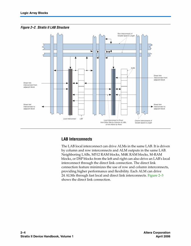
Each LAB consists of eight ALMs, carry chains, shared arithmetic chains, LAB control signals, local interconnect, and register chain connection lines. The local interconnect transfers signals between ALMs in the same LAB. Register chain connections transfer the output of an ALM register to the adjacent ALM register in an LAB. The Quartus® II Compiler places associated logic in an LAB or adjacent LABs, allowing the use of local, shared arithmetic chain, and register chain connections for performance and area efficiency. Figure 2–2 shows the Stratix II LAB structure.
Table 2–1. Stratix II Device Resources
Device M512 RAM Columns/Blocks
M4K RAM Columns/Blocks
M-RAM Blocks
DSP Block Columns/Blocks
LAB Columns LAB Rows
EP2S15 4 / 104 3 / 78 0 2 / 12 30 26
EP2S30 6 / 202 4 / 144 1 2 / 16 49 36
EP2S60 7 / 329 5 / 255 2 3 / 36 62 51
EP2S90 8 / 488 6 / 408 4 3 / 48 71 68
EP2S130 9 / 699 7 / 609 6 3 / 63 81 87
EP2S180 11 / 930 8 / 768 9 4 / 96 100 96
2–4 Altera CorporationStratix II Device Handbook, Volume 1 April 2006
Logic Array Blocks
Figure 2–2. Stratix II LAB Structure
LAB Interconnects
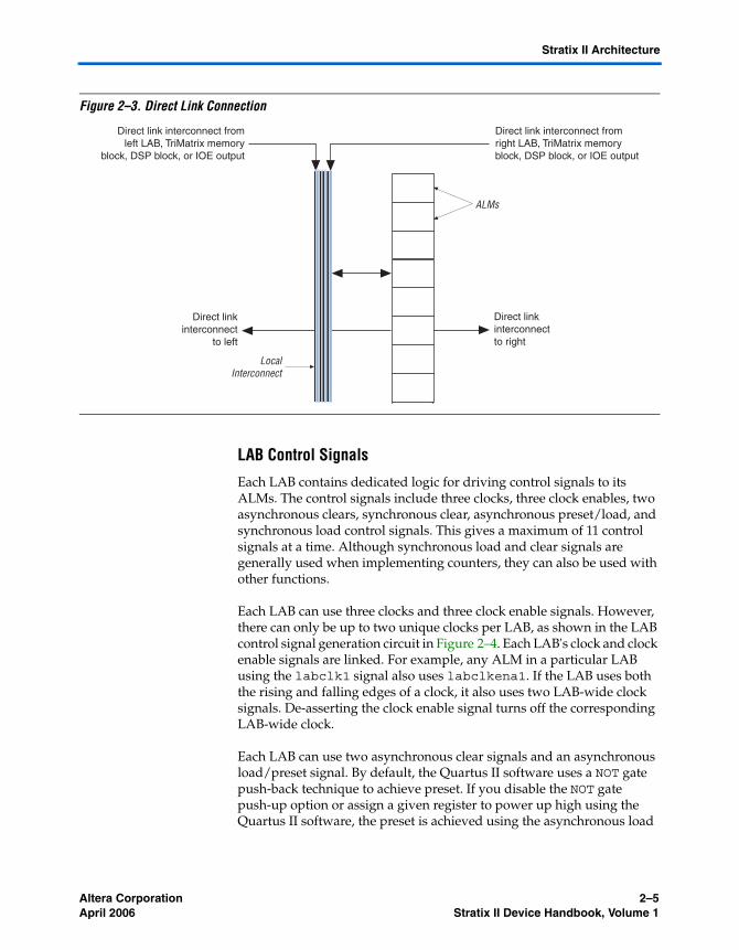
The LAB local interconnect can drive ALMs in the same LAB. It is driven by column and row interconnects and ALM outputs in the same LAB. Neighboring LABs, M512 RAM blocks, M4K RAM blocks, M-RAM blocks, or DSP blocks from the left and right can also drive an LAB's local interconnect through the direct link connection. The direct link connection feature minimizes the use of row and column interconnects, providing higher performance and flexibility. Each ALM can drive 24 ALMs through fast local and direct link interconnects. Figure 2–3 shows the direct link connection.
Direct linkinterconnect fromadjacent block
Direct linkinterconnect toadjacent block
Row Interconnects ofVariable Speed & Length
Column Interconnects ofVariable Speed & Length
Local Interconnect is Driven from Either Side by Columns & LABs,
& from Above by Rows
Local Interconnect LAB
Direct linkinterconnect from adjacent block
Direct linkinterconnect toadjacent block
ALMs
Altera Corporation 2–5April 2006 Stratix II Device Handbook, Volume 1
Stratix II Architecture
Figure 2–3. Direct Link Connection
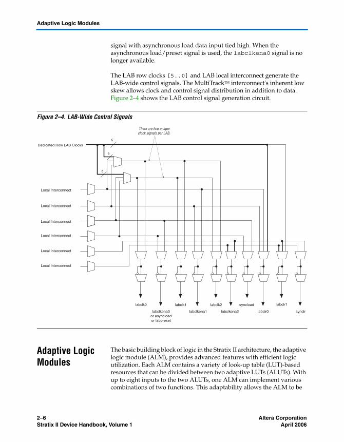
LAB Control Signals
Each LAB contains dedicated logic for driving control signals to its ALMs. The control signals include three clocks, three clock enables, two asynchronous clears, synchronous clear, asynchronous preset/load, and synchronous load control signals. This gives a maximum of 11 control signals at a time. Although synchronous load and clear signals are generally used when implementing counters, they can also be used with other functions.
Each LAB can use three clocks and three clock enable signals. However, there can only be up to two unique clocks per LAB, as shown in the LAB control signal generation circuit in Figure 2–4. Each LAB's clock and clock enable signals are linked. For example, any ALM in a particular LAB using the labclk1 signal also uses labclkena1. If the LAB uses both the rising and falling edges of a clock, it also uses two LAB-wide clock signals. De-asserting the clock enable signal turns off the corresponding LAB-wide clock.
Each LAB can use two asynchronous clear signals and an asynchronous load/preset signal. By default, the Quartus II software uses a NOT gate push-back technique to achieve preset. If you disable the NOT gate push-up option or assign a given register to power up high using the Quartus II software, the preset is achieved using the asynchronous load
ALMs
Direct linkinterconnectto right
Direct link interconnect fromright LAB, TriMatrix memoryblock, DSP block, or IOE output
Direct link interconnect fromleft LAB, TriMatrix memory
block, DSP block, or IOE output
LocalInterconnect
Direct linkinterconnect
to left
2–6 Altera CorporationStratix II Device Handbook, Volume 1 April 2006
Adaptive Logic Modules
signal with asynchronous load data input tied high. When the asynchronous load/preset signal is used, the labclkena0 signal is no longer available.
The LAB row clocks [5..0] and LAB local interconnect generate the LAB-wide control signals. The MultiTrackTM interconnect's inherent low skew allows clock and control signal distribution in addition to data. Figure 2–4 shows the LAB control signal generation circuit.
Figure 2–4. LAB-Wide Control Signals
Adaptive Logic Modules
The basic building block of logic in the Stratix II architecture, the adaptive logic module (ALM), provides advanced features with efficient logic utilization. Each ALM contains a variety of look-up table (LUT)-based resources that can be divided between two adaptive LUTs (ALUTs). With up to eight inputs to the two ALUTs, one ALM can implement various combinations of two functions. This adaptability allows the ALM to be
Dedicated Row LAB Clocks
Local Interconnect
Local Interconnect
Local Interconnect
Local Interconnect
Local Interconnect
Local Interconnect
labclk2 syncload
labclkena0or asyncloador labpreset
labclk0 labclk1 labclr1
labclkena1 labclkena2 labclr0 synclr
6
6
6
There are two uniqueclock signals per LAB.
Altera Corporation 2–7April 2006 Stratix II Device Handbook, Volume 1
Stratix II Architecture
completely backward-compatible with four-input LUT architectures. One ALM can also implement any function of up to six inputs and certain seven-input functions.
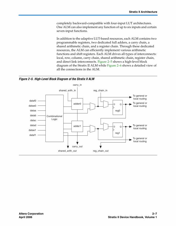
In addition to the adaptive LUT-based resources, each ALM contains two programmable registers, two dedicated full adders, a carry chain, a shared arithmetic chain, and a register chain. Through these dedicated resources, the ALM can efficiently implement various arithmetic functions and shift registers. Each ALM drives all types of interconnects: local, row, column, carry chain, shared arithmetic chain, register chain, and direct link interconnects. Figure 2–5 shows a high-level block diagram of the Stratix II ALM while Figure 2–6 shows a detailed view of all the connections in the ALM.
Figure 2–5. High-Level Block Diagram of the Stratix II ALM
D QTo general orlocal routing
reg0
To general orlocal routing
datae0
dataf0
shared_arith_in
shared_arith_out
reg_chain_in
reg_chain_out
adder0
dataa
datab
datac
datad
CombinationalLogic
datae1
dataf1
D QTo general orlocal routing
reg1
To general orlocal routing
adder1
carry_in
carry_out
2–8 Altera CorporationStratix II Device Handbook, Volume 1 April 2006
Adaptive Logic Modules
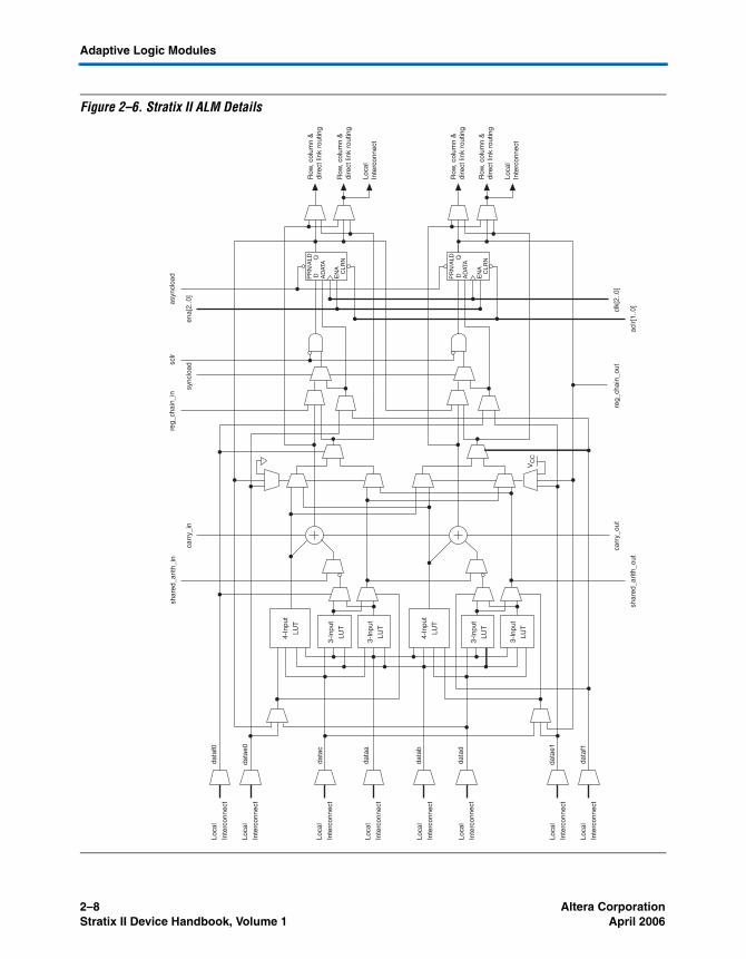
Figure 2–6. Stratix II ALM Details
PR
N/A
LD
CLR
N
D AD
ATA
EN
A
Q
PR
N/A
LD
CLR
N
D AD
ATA
EN
A
Q
4-In
put
LUT
3-In
put
LUT
3-In
put
LUT
4-In
put
LUT
3-In
put
LUT
3-In
put
LUT
data
a
data
c
data
e0
data
f0
data
f1
data
e1
data
b
data
d
VC
C
reg_
chai
n_in
sclr
asyn
cloa
d
sync
load
ena[
2..0
]
shar
ed_a
rith_
in
carr
y_in
carr
y_ou
tcl
k[2.
.0]
Loca
lIn
terc
onne
ct
Row
, col
umn
&di
rect
link
rou
ting
Row
, col
umn
&di
rect
link
rou
ting
Loca
lIn
terc
onne
ct
Row
, col
umn
&di
rect
link
rou
ting
Row
, col
umn
&di
rect
link
rou
ting
reg_
chai
n_ou
t
shar
ed_a
rith_
out
aclr[
1..0
]
Loca
l
Inte
rcon
nect
Loca
l
Inte
rcon
nect
Loca
l
Inte
rcon
nect
Loca
l
Inte
rcon
nect
Loca
l
Inte
rcon
nect
Loca
l
Inte
rcon
nect
Loca
l
Inte
rcon
nect
Loca
l
Inte
rcon
nect
Altera Corporation 2–9April 2006 Stratix II Device Handbook, Volume 1
Stratix II Architecture
One ALM contains two programmable registers. Each register has data, clock, clock enable, synchronous and asynchronous clear, asynchronous load data, and synchronous and asynchronous load/preset inputs. Global signals, general-purpose I/O pins, or any internal logic can drive the register's clock and clear control signals. Either general-purpose I/O pins or internal logic can drive the clock enable, preset, asynchronous load, and asynchronous load data. The asynchronous load data input comes from the datae or dataf input of the ALM, which are the same inputs that can be used for register packing. For combinational functions, the register is bypassed and the output of the LUT drives directly to the outputs of the ALM.
Each ALM has two sets of outputs that drive the local, row, and column routing resources. The LUT, adder, or register output can drive these output drivers independently (see Figure 2–6). For each set of output drivers, two ALM outputs can drive column, row, or direct link routing connections, and one of these ALM outputs can also drive local interconnect resources. This allows the LUT or adder to drive one output while the register drives another output. This feature, called register packing, improves device utilization because the device can use the register and the combinational logic for unrelated functions. Another special packing mode allows the register output to feed back into the LUT of the same ALM so that the register is packed with its own fan-out LUT. This provides another mechanism for improved fitting. The ALM can also drive out registered and unregistered versions of the LUT or adder output.
See the Performance & Logic Efficiency Analysis of Stratix II Devices White Paper for more information on the efficiencies of the Stratix II ALM and comparisons with previous architectures.
ALM Operating Modes
The Stratix II ALM can operate in one of the following modes:
■ Normal mode■ Extended LUT mode■ Arithmetic mode■ Shared arithmetic mode
Each mode uses ALM resources differently. In each mode, eleven available inputs to the ALM--the eight data inputs from the LAB local interconnect; carry-in from the previous ALM or LAB; the shared arithmetic chain connection from the previous ALM or LAB; and the register chain connection--are directed to different destinations to implement the desired logic function. LAB-wide signals provide clock, asynchronous clear, asynchronous preset/load, synchronous clear,
2–10 Altera CorporationStratix II Device Handbook, Volume 1 April 2006
Adaptive Logic Modules
synchronous load, and clock enable control for the register. These LAB-wide signals are available in all ALM modes. See the “LAB Control Signals” section for more information on the LAB-wide control signals.
The Quartus II software and supported third-party synthesis tools, in conjunction with parameterized functions such as library of parameterized modules (LPM) functions, automatically choose the appropriate mode for common functions such as counters, adders, subtractors, and arithmetic functions. If required, you can also create special-purpose functions that specify which ALM operating mode to use for optimal performance.
Normal Mode
The normal mode is suitable for general logic applications and combinational functions. In this mode, up to eight data inputs from the LAB local interconnect are inputs to the combinational logic. The normal mode allows two functions to be implemented in one Stratix II ALM, or an ALM to implement a single function of up to six inputs. The ALM can support certain combinations of completely independent functions and various combinations of functions which have common inputs. Figure 2–7 shows the supported LUT combinations in normal mode.
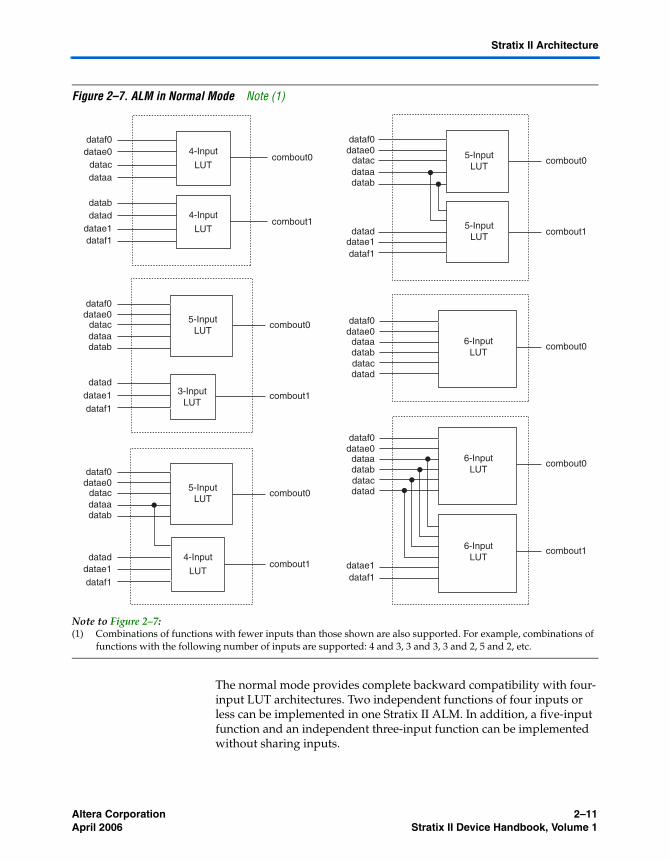
Altera Corporation 2–11April 2006 Stratix II Device Handbook, Volume 1
Stratix II Architecture
Figure 2–7. ALM in Normal Mode Note (1)
Note to Figure 2–7:(1) Combinations of functions with fewer inputs than those shown are also supported. For example, combinations of
functions with the following number of inputs are supported: 4 and 3, 3 and 3, 3 and 2, 5 and 2, etc.
The normal mode provides complete backward compatibility with four-input LUT architectures. Two independent functions of four inputs or less can be implemented in one Stratix II ALM. In addition, a five-input function and an independent three-input function can be implemented without sharing inputs.
6-InputLUT
dataf0datae0
dataf0datae0
dataadatab
dataadatab
datab
datac
datac
dataf0datae0
dataadatac
6-InputLUT
datad
datad
datae1
combout0
combout1
combout0
combout1
combout0
combout1
dataf1
datae1dataf1
dataddatae1dataf1
4-Input
LUT
4-Input
LUT
4-Input
LUT
6-InputLUT
dataf0datae0
dataadatabdatacdatad
combout0
5-InputLUT
5-InputLUT
dataf0datae0
dataadatab
datac
datad
combout0
combout1datae1dataf1
5-InputLUT
dataf0datae0
dataadatab
datac
datad
combout0
combout1datae1dataf1
5-InputLUT
3-InputLUT
2–12 Altera CorporationStratix II Device Handbook, Volume 1 April 2006
Adaptive Logic Modules
For the packing of two five-input functions into one ALM, the functions must have at least two common inputs. The common inputs are dataa and datab. The combination of a four-input function with a five-input function requires one common input (either dataa or datab).
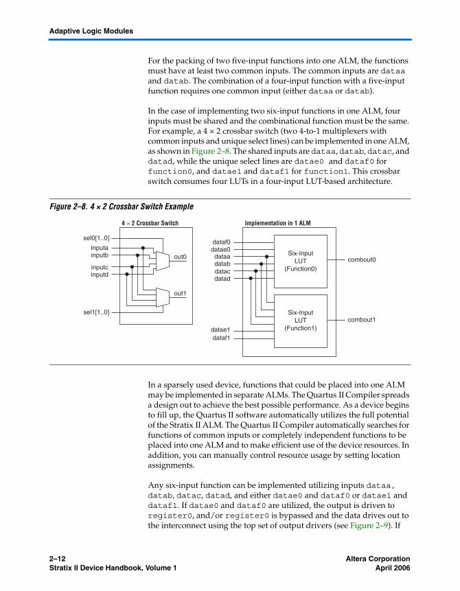
In the case of implementing two six-input functions in one ALM, four inputs must be shared and the combinational function must be the same. For example, a 4 × 2 crossbar switch (two 4-to-1 multiplexers with common inputs and unique select lines) can be implemented in one ALM, as shown in Figure 2–8. The shared inputs are dataa, datab, datac, and datad, while the unique select lines are datae0 and dataf0 for function0, and datae1 and dataf1 for function1. This crossbar switch consumes four LUTs in a four-input LUT-based architecture.
Figure 2–8. 4 × 2 Crossbar Switch Example
In a sparsely used device, functions that could be placed into one ALM may be implemented in separate ALMs. The Quartus II Compiler spreads a design out to achieve the best possible performance. As a device begins to fill up, the Quartus II software automatically utilizes the full potential of the Stratix II ALM. The Quartus II Compiler automatically searches for functions of common inputs or completely independent functions to be placed into one ALM and to make efficient use of the device resources. In addition, you can manually control resource usage by setting location assignments.
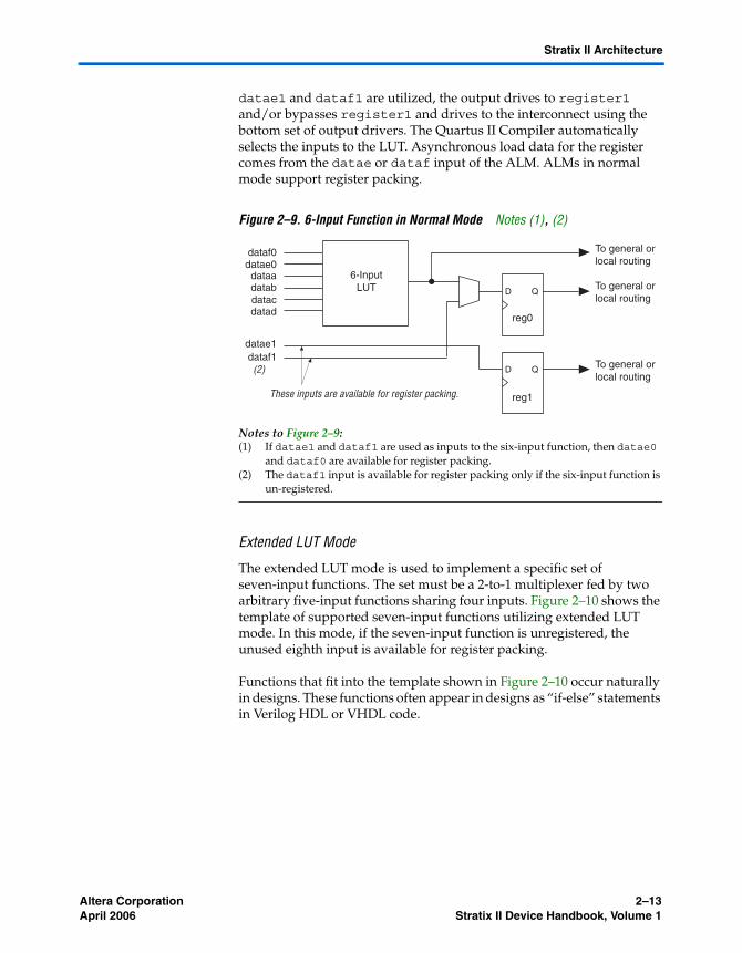
Any six-input function can be implemented utilizing inputs dataa, datab, datac, datad, and either datae0 and dataf0 or datae1 and dataf1. If datae0 and dataf0 are utilized, the output is driven to register0, and/or register0 is bypassed and the data drives out to the interconnect using the top set of output drivers (see Figure 2–9). If
Six-InputLUT
(Function0)
dataf0datae0
dataadatabdatac
Six-InputLUT
(Function1)
datad
datae1
combout0
combout1
dataf1
inputa
sel0[1..0]
sel1[1..0]
inputb
inputcinputd
out0
out1
4 × 2 Crossbar Switch Implementation in 1 ALM
Altera Corporation 2–13April 2006 Stratix II Device Handbook, Volume 1
Stratix II Architecture
datae1 and dataf1 are utilized, the output drives to register1 and/or bypasses register1 and drives to the interconnect using the bottom set of output drivers. The Quartus II Compiler automatically selects the inputs to the LUT. Asynchronous load data for the register comes from the datae or dataf input of the ALM. ALMs in normal mode support register packing.
Figure 2–9. 6-Input Function in Normal Mode Notes (1), (2)
Notes to Figure 2–9:(1) If datae1 and dataf1 are used as inputs to the six-input function, then datae0
and dataf0 are available for register packing.(2) The dataf1 input is available for register packing only if the six-input function is
un-registered.
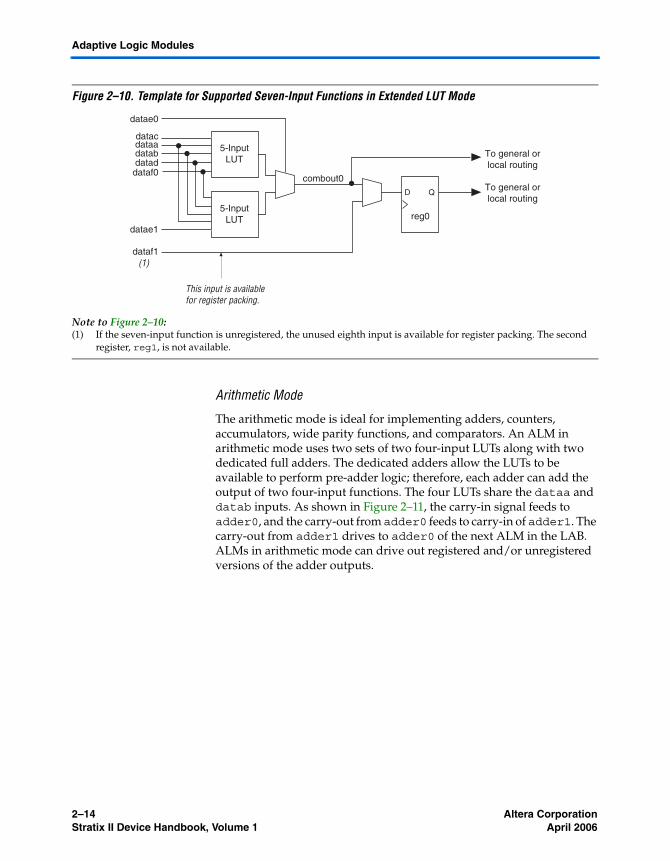
Extended LUT Mode
The extended LUT mode is used to implement a specific set of seven-input functions. The set must be a 2-to-1 multiplexer fed by two arbitrary five-input functions sharing four inputs. Figure 2–10 shows the template of supported seven-input functions utilizing extended LUT mode. In this mode, if the seven-input function is unregistered, the unused eighth input is available for register packing.
Functions that fit into the template shown in Figure 2–10 occur naturally in designs. These functions often appear in designs as “if-else” statements in Verilog HDL or VHDL code.
6-InputLUT
dataf0datae0
dataadatabdatacdatad
datae1dataf1
D Q
D Q
To general orlocal routing
To general orlocal routing
To general orlocal routing
reg0
reg1These inputs are available for register packing.
(2)
2–14 Altera CorporationStratix II Device Handbook, Volume 1 April 2006
Adaptive Logic Modules
Figure 2–10. Template for Supported Seven-Input Functions in Extended LUT Mode
Note to Figure 2–10:(1) If the seven-input function is unregistered, the unused eighth input is available for register packing. The second
register, reg1, is not available.
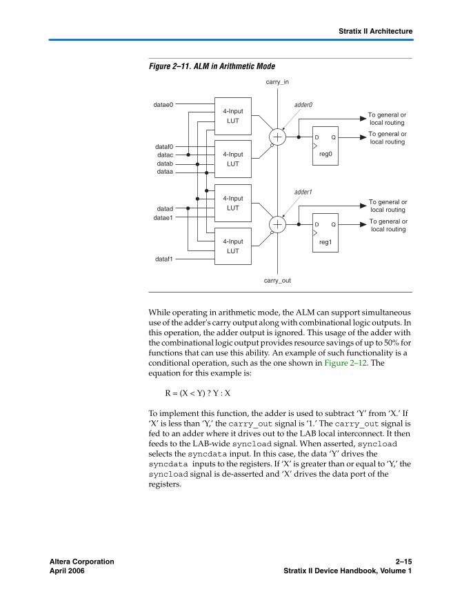
Arithmetic Mode
The arithmetic mode is ideal for implementing adders, counters, accumulators, wide parity functions, and comparators. An ALM in arithmetic mode uses two sets of two four-input LUTs along with two dedicated full adders. The dedicated adders allow the LUTs to be available to perform pre-adder logic; therefore, each adder can add the output of two four-input functions. The four LUTs share the dataa and datab inputs. As shown in Figure 2–11, the carry-in signal feeds to adder0, and the carry-out from adder0 feeds to carry-in of adder1. The carry-out from adder1 drives to adder0 of the next ALM in the LAB. ALMs in arithmetic mode can drive out registered and/or unregistered versions of the adder outputs.
datae0
combout0
5-InputLUT
5-InputLUT
datacdataadatabdataddataf0
datae1
dataf1
D QTo general orlocal routing
To general orlocal routing
reg0
This input is availablefor register packing.
(1)
Altera Corporation 2–15April 2006 Stratix II Device Handbook, Volume 1
Stratix II Architecture
Figure 2–11. ALM in Arithmetic Mode
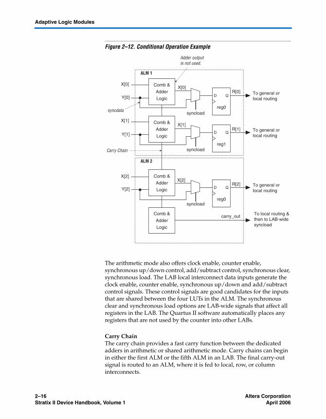
While operating in arithmetic mode, the ALM can support simultaneous use of the adder's carry output along with combinational logic outputs. In this operation, the adder output is ignored. This usage of the adder with the combinational logic output provides resource savings of up to 50% for functions that can use this ability. An example of such functionality is a conditional operation, such as the one shown in Figure 2–12. The equation for this example is:
R = (X < Y) ? Y : X
To implement this function, the adder is used to subtract ‘Y’ from ‘X.’ If ‘X’ is less than ‘Y,’ the carry_out signal is ‘1.’ The carry_out signal is fed to an adder where it drives out to the LAB local interconnect. It then feeds to the LAB-wide syncload signal. When asserted, syncload selects the syncdata input. In this case, the data ‘Y’ drives the syncdata inputs to the registers. If ‘X’ is greater than or equal to ‘Y,’ the syncload signal is de-asserted and ‘X’ drives the data port of the registers.
dataf0
datae0
carry_in
carry_out
dataadatabdatac
dataddatae1
dataf1
D Q
D Q
To general orlocal routing
To general orlocal routing
reg0
reg1
To general orlocal routing
To general orlocal routing
4-Input
LUT
4-Input
LUT
4-Input
LUT
4-Input
LUT
adder1
adder0
2–16 Altera CorporationStratix II Device Handbook, Volume 1 April 2006
Adaptive Logic Modules
Figure 2–12. Conditional Operation Example
The arithmetic mode also offers clock enable, counter enable, synchronous up/down control, add/subtract control, synchronous clear, synchronous load. The LAB local interconnect data inputs generate the clock enable, counter enable, synchronous up/down and add/subtract control signals. These control signals are good candidates for the inputs that are shared between the four LUTs in the ALM. The synchronous clear and synchronous load options are LAB-wide signals that affect all registers in the LAB. The Quartus II software automatically places any registers that are not used by the counter into other LABs.
Carry ChainThe carry chain provides a fast carry function between the dedicated adders in arithmetic or shared arithmetic mode. Carry chains can begin in either the first ALM or the fifth ALM in an LAB. The final carry-out signal is routed to an ALM, where it is fed to local, row, or column interconnects.
Y[1]
Y[0]
X[0]X[0]
carry_out
X[2]X[2]
X[1]X[1]
Y[2]
D QTo general orlocal routing
reg0
Comb &
Adder
Logic
Comb &
Adder
Logic
Comb &
Adder
Logic
Comb &
Adder
Logic
D QTo general orlocal routing
reg1
D QTo general orlocal routing
To local routing &then to LAB-widesyncload
reg0
syncload
syncload
syncload
ALM 1
ALM 2
R[0]
R[1]
R[2]
Carry Chain
Adder outputis not used.
syncdata
Altera Corporation 2–17April 2006 Stratix II Device Handbook, Volume 1
Stratix II Architecture
The Quartus II Compiler automatically creates carry chain logic during design processing, or you can create it manually during design entry. Parameterized functions such as LPM functions automatically take advantage of carry chains for the appropriate functions.
The Quartus II Compiler creates carry chains longer than 16 (8 ALMs in arithmetic or shared arithmetic mode) by linking LABs together automatically. For enhanced fitting, a long carry chain runs vertically allowing fast horizontal connections to TriMatrix memory and DSP blocks. A carry chain can continue as far as a full column.
To avoid routing congestion in one small area of the device when a high fan-in arithmetic function is implemented, the LAB can support carry chains that only utilize either the top half or the bottom half of the LAB before connecting to the next LAB. This leaves the other half of the ALMs in the LAB available for implementing narrower fan-in functions in normal mode. Carry chains that use the top four ALMs in the first LAB carry into the top half of the ALMs in the next LAB within the column. Carry chains that use the bottom four ALMs in the first LAB carry into the bottom half of the ALMs in the next LAB within the column. Every other column of LABs is top-half bypassable, while the other LAB columns are bottom-half bypassable.
See the “MultiTrack Interconnect” section for more information on carry chain interconnect.
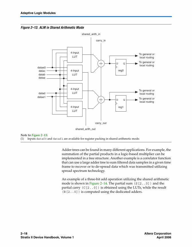
Shared Arithmetic Mode
In shared arithmetic mode, the ALM can implement a three-input add. In this mode, the ALM is configured with four 4-input LUTs. Each LUT either computes the sum of three inputs or the carry of three inputs. The output of the carry computation is fed to the next adder (either to adder1 in the same ALM or to adder0 of the next ALM in the LAB) via a dedicated connection called the shared arithmetic chain. This shared arithmetic chain can significantly improve the performance of an adder tree by reducing the number of summation stages required to implement an adder tree. Figure 2–13 shows the ALM in shared arithmetic mode.
2–18 Altera CorporationStratix II Device Handbook, Volume 1 April 2006
Adaptive Logic Modules
Figure 2–13. ALM in Shared Arithmetic Mode
Note to Figure 2–13:(1) Inputs dataf0 and dataf1 are available for register packing in shared arithmetic mode.
Adder trees can be found in many different applications. For example, the summation of the partial products in a logic-based multiplier can be implemented in a tree structure. Another example is a correlator function that can use a large adder tree to sum filtered data samples in a given time frame to recover or to de-spread data which was transmitted utilizing spread spectrum technology.
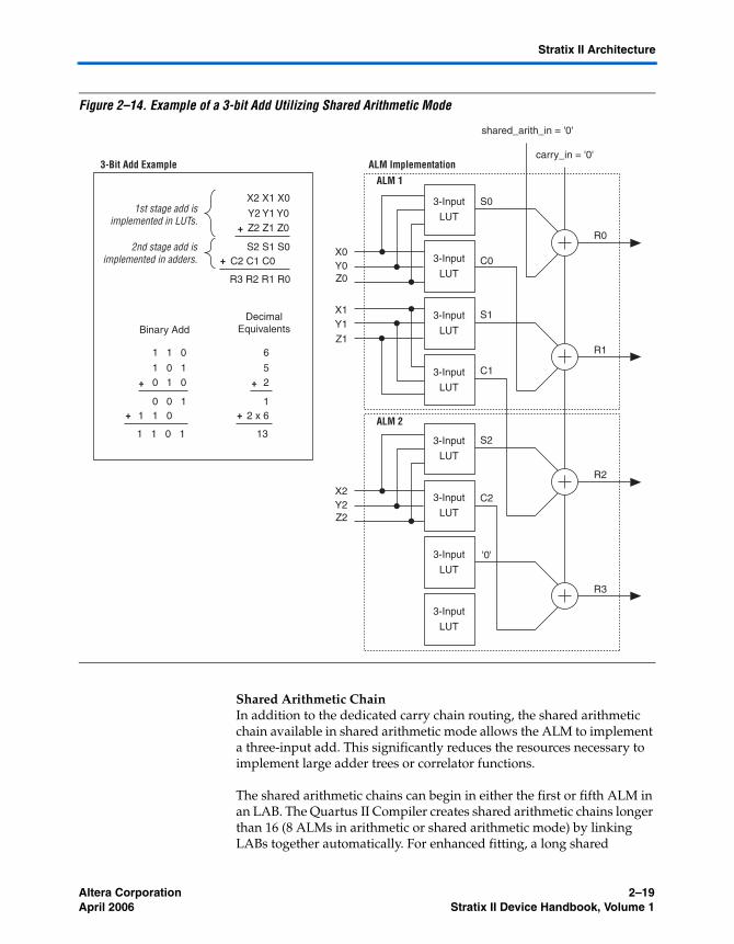
An example of a three-bit add operation utilizing the shared arithmetic mode is shown in Figure 2–14. The partial sum (S[2..0]) and the partial carry (C[2..0]) is obtained using the LUTs, while the result (R[2..0]) is computed using the dedicated adders.
datae0
carry_in
shared_arith_in
shared_arith_out
carry_out
dataadatabdatac
dataddatae1
D Q
D Q
To general orlocal routing
To general orlocal routing
reg0
reg1
To general orlocal routing
To general orlocal routing
4-Input
LUT
4-Input
LUT
4-Input
LUT
4-Input
LUT
Altera Corporation 2–19April 2006 Stratix II Device Handbook, Volume 1
Stratix II Architecture
Figure 2–14. Example of a 3-bit Add Utilizing Shared Arithmetic Mode
Shared Arithmetic ChainIn addition to the dedicated carry chain routing, the shared arithmetic chain available in shared arithmetic mode allows the ALM to implement a three-input add. This significantly reduces the resources necessary to implement large adder trees or correlator functions.
The shared arithmetic chains can begin in either the first or fifth ALM in an LAB. The Quartus II Compiler creates shared arithmetic chains longer than 16 (8 ALMs in arithmetic or shared arithmetic mode) by linking LABs together automatically. For enhanced fitting, a long shared
carry_in = '0'
shared_arith_in = '0'
Z0Y0X0
Binary AddDecimal
Equivalents
+
Z1
X1
R0
C0
S0
S1
S2
C1
C2
'0'
R1
Y1
3-Input
LUT
3-Input
LUT
3-Input
LUT
3-Input
LUT
Z2Y2X2
R2
R3
3-Input
LUT
3-Input
LUT
3-Input
LUT
3-Input
LUT
ALM 1
3-Bit Add Example ALM Implementation
ALM 2
X2 X1 X0
Y2 Y1 Y0Z2 Z1 Z0
S2 S1 S0C2 C1 C0
R3 R2 R1 R0
+
+
1 1 0
1 0 10 1 0
0 0 11 1 0
1 1 0 1
+
+
6
52
12 x 6
13
+
2nd stage add isimplemented in adders.
1st stage add isimplemented in LUTs.
2–20 Altera CorporationStratix II Device Handbook, Volume 1 April 2006
Adaptive Logic Modules
arithmetic chain runs vertically allowing fast horizontal connections to TriMatrix memory and DSP blocks. A shared arithmetic chain can continue as far as a full column.
Similar to the carry chains, the shared arithmetic chains are also top- or bottom-half bypassable. This capability allows the shared arithmetic chain to cascade through half of the ALMs in a LAB while leaving the other half available for narrower fan-in functionality. Every other LAB column is top-half bypassable, while the other LAB columns are bottom-half bypassable.
See the “MultiTrack Interconnect” section for more information on shared arithmetic chain interconnect.
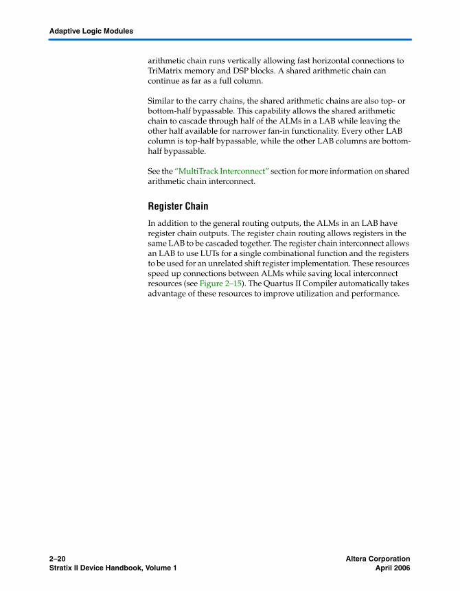
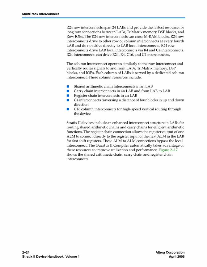
Register Chain
In addition to the general routing outputs, the ALMs in an LAB have register chain outputs. The register chain routing allows registers in the same LAB to be cascaded together. The register chain interconnect allows an LAB to use LUTs for a single combinational function and the registers to be used for an unrelated shift register implementation. These resources speed up connections between ALMs while saving local interconnect resources (see Figure 2–15). The Quartus II Compiler automatically takes advantage of these resources to improve utilization and performance.
Altera Corporation 2–21April 2006 Stratix II Device Handbook, Volume 1
Stratix II Architecture
Figure 2–15. Register Chain within an LAB Note (1)
Note to Figure 2–15:(1) The combinational or adder logic can be utilized to implement an unrelated, un-registered function.
See the “MultiTrack Interconnect” section for more information on register chain interconnect.
D QTo general orlocal routing
reg0
To general orlocal routing
reg_chain_in
adder0
D QTo general orlocal routing
reg1
To general orlocal routing
adder1
D QTo general orlocal routing
reg0
To general orlocal routing
reg_chain_out
adder0
D QTo general orlocal routing
reg1
To general orlocal routing
adder1
From Previous ALMWithin The LAB
To Next ALMwithin the LAB
Combinational
Logic
CombinationalLogic
2–22 Altera CorporationStratix II Device Handbook, Volume 1 April 2006
MultiTrack Interconnect
Clear & Preset Logic Control
LAB-wide signals control the logic for the register's clear and load/preset signals. The ALM directly supports an asynchronous clear and preset function. The register preset is achieved through the asynchronous load of a logic high. The direct asynchronous preset does not require a NOT-gate push-back technique. Stratix II devices support simultaneous asynchronous load/preset, and clear signals. An asynchronous clear signal takes precedence if both signals are asserted simultaneously. Each LAB supports up to two clears and one load/preset signal.
In addition to the clear and load/preset ports, Stratix II devices provide a device-wide reset pin (DEV_CLRn) that resets all registers in the device. An option set before compilation in the Quartus II software controls this pin. This device-wide reset overrides all other control signals.
MultiTrack Interconnect
In the Stratix II architecture, connections between ALMs, TriMatrix memory, DSP blocks, and device I/O pins are provided by the MultiTrack interconnect structure with DirectDriveTM technology. The MultiTrack interconnect consists of continuous, performance-optimized routing lines of different lengths and speeds used for inter- and intra-design block connectivity. The Quartus II Compiler automatically places critical design paths on faster interconnects to improve design performance.
DirectDrive technology is a deterministic routing technology that ensures identical routing resource usage for any function regardless of placement in the device. The MultiTrack interconnect and DirectDrive technology simplify the integration stage of block-based designing by eliminating the re-optimization cycles that typically follow design changes and additions.
The MultiTrack interconnect consists of row and column interconnects that span fixed distances. A routing structure with fixed length resources for all devices allows predictable and repeatable performance when migrating through different device densities. Dedicated row interconnects route signals to and from LABs, DSP blocks, and TriMatrix memory in the same row. These row resources include:
■ Direct link interconnects between LABs and adjacent blocks■ R4 interconnects traversing four blocks to the right or left■ R24 row interconnects for high-speed access across the length of the
device
Altera Corporation 2–23April 2006 Stratix II Device Handbook, Volume 1
Stratix II Architecture
The direct link interconnect allows an LAB, DSP block, or TriMatrix memory block to drive into the local interconnect of its left and right neighbors and then back into itself. This provides fast communication between adjacent LABs and/or blocks without using row interconnect resources.
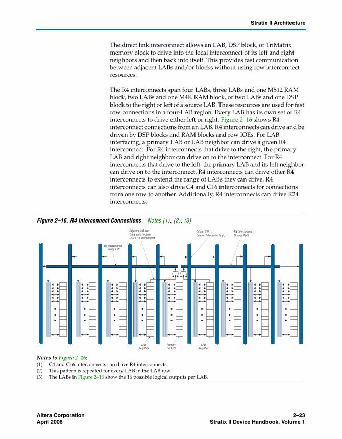
The R4 interconnects span four LABs, three LABs and one M512 RAM block, two LABs and one M4K RAM block, or two LABs and one DSP block to the right or left of a source LAB. These resources are used for fast row connections in a four-LAB region. Every LAB has its own set of R4 interconnects to drive either left or right. Figure 2–16 shows R4 interconnect connections from an LAB. R4 interconnects can drive and be driven by DSP blocks and RAM blocks and row IOEs. For LAB interfacing, a primary LAB or LAB neighbor can drive a given R4 interconnect. For R4 interconnects that drive to the right, the primary LAB and right neighbor can drive on to the interconnect. For R4 interconnects that drive to the left, the primary LAB and its left neighbor can drive on to the interconnect. R4 interconnects can drive other R4 interconnects to extend the range of LABs they can drive. R4 interconnects can also drive C4 and C16 interconnects for connections from one row to another. Additionally, R4 interconnects can drive R24 interconnects.
Figure 2–16. R4 Interconnect Connections Notes (1), (2), (3)
Notes to Figure 2–16:(1) C4 and C16 interconnects can drive R4 interconnects.(2) This pattern is repeated for every LAB in the LAB row.(3) The LABs in Figure 2–16 show the 16 possible logical outputs per LAB.
PrimaryLAB (2)
R4 InterconnectDriving Left
Adjacent LAB canDrive onto AnotherLAB's R4 Interconnect
C4 and C16Column Interconnects (1)
R4 InterconnectDriving Right
LABNeighbor
LABNeighbor
2–24 Altera CorporationStratix II Device Handbook, Volume 1 April 2006
MultiTrack Interconnect
R24 row interconnects span 24 LABs and provide the fastest resource for long row connections between LABs, TriMatrix memory, DSP blocks, and Row IOEs. The R24 row interconnects can cross M-RAM blocks. R24 row interconnects drive to other row or column interconnects at every fourth LAB and do not drive directly to LAB local interconnects. R24 row interconnects drive LAB local interconnects via R4 and C4 interconnects. R24 interconnects can drive R24, R4, C16, and C4 interconnects.
The column interconnect operates similarly to the row interconnect and vertically routes signals to and from LABs, TriMatrix memory, DSP blocks, and IOEs. Each column of LABs is served by a dedicated column interconnect. These column resources include:
■ Shared arithmetic chain interconnects in an LAB■ Carry chain interconnects in an LAB and from LAB to LAB■ Register chain interconnects in an LAB■ C4 interconnects traversing a distance of four blocks in up and down
direction■ C16 column interconnects for high-speed vertical routing through
the device
Stratix II devices include an enhanced interconnect structure in LABs for routing shared arithmetic chains and carry chains for efficient arithmetic functions. The register chain connection allows the register output of one ALM to connect directly to the register input of the next ALM in the LAB for fast shift registers. These ALM to ALM connections bypass the local interconnect. The Quartus II Compiler automatically takes advantage of these resources to improve utilization and performance. Figure 2–17 shows the shared arithmetic chain, carry chain and register chain interconnects.
Altera Corporation 2–25April 2006 Stratix II Device Handbook, Volume 1
Stratix II Architecture
Figure 2–17. Shared Arithmetic Chain, Carry Chain & Register Chain Interconnects
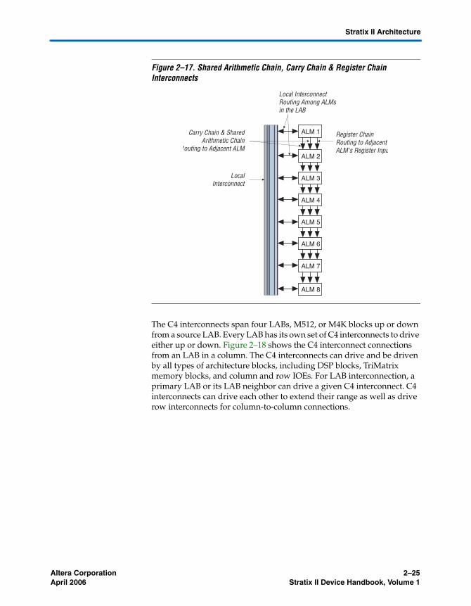
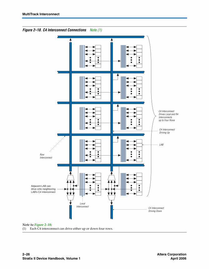
The C4 interconnects span four LABs, M512, or M4K blocks up or down from a source LAB. Every LAB has its own set of C4 interconnects to drive either up or down. Figure 2–18 shows the C4 interconnect connections from an LAB in a column. The C4 interconnects can drive and be driven by all types of architecture blocks, including DSP blocks, TriMatrix memory blocks, and column and row IOEs. For LAB interconnection, a primary LAB or its LAB neighbor can drive a given C4 interconnect. C4 interconnects can drive each other to extend their range as well as drive row interconnects for column-to-column connections.
ALM 1
ALM 2
ALM 3
ALM 4
ALM 5
ALM 6
ALM 8
ALM 7
Carry Chain & SharedArithmetic Chain
Routing to Adjacent ALM
LocalInterconnect
Register ChainRouting to AdjacentALM's Register Inpu
Local InterconnectRouting Among ALMsin the LAB
2–26 Altera CorporationStratix II Device Handbook, Volume 1 April 2006
MultiTrack Interconnect
Figure 2–18. C4 Interconnect Connections Note (1)
Note to Figure 2–18:(1) Each C4 interconnect can drive either up or down four rows.
C4 InterconnectDrives Local and R4Interconnectsup to Four Rows
Adjacent LAB candrive onto neighboringLAB's C4 interconnect
C4 InterconnectDriving Up
C4 InterconnectDriving Down
LAB
RowInterconnect
LocalInterconnect
Altera Corporation 2–27April 2006 Stratix II Device Handbook, Volume 1
Stratix II Architecture
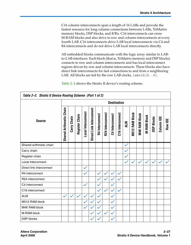
C16 column interconnects span a length of 16 LABs and provide the fastest resource for long column connections between LABs, TriMatrix memory blocks, DSP blocks, and IOEs. C16 interconnects can cross M-RAM blocks and also drive to row and column interconnects at every fourth LAB. C16 interconnects drive LAB local interconnects via C4 and R4 interconnects and do not drive LAB local interconnects directly.
All embedded blocks communicate with the logic array similar to LAB-to-LAB interfaces. Each block (that is, TriMatrix memory and DSP blocks) connects to row and column interconnects and has local interconnect regions driven by row and column interconnects. These blocks also have direct link interconnects for fast connections to and from a neighboring LAB. All blocks are fed by the row LAB clocks, labclk[5..0].
Table 2–2 shows the Stratix II device’s routing scheme.
Table 2–2. Stratix II Device Routing Scheme (Part 1 of 2)
Source
Destination
Shar
ed A
rithm
etic
Cha
in
Carr
y Ch
ain
Regi
ster
Cha
in
Loca
l Int
erco
nnec
t
Dire
ct L
ink
Inte
rcon
nect
R4 In
terc
onne
ct
R24
Inte
rcon
nect
C4 In
terc
onne
ct
C16
Inte
rcon
nect
ALM
M51
2 RA
M B
lock
M4K
RAM
Blo
ck
M-R
AM B
lock
DSP
Bloc
ks
Colu
mn
IOE
Row
IOE
Shared arithmetic chain v
Carry chain v
Register chain v
Local interconnect v v v v v v v
Direct link interconnect v
R4 interconnect v v v v v
R24 interconnect v v v v
C4 interconnect v v v
C16 interconnect v v v v
ALM v v v v v v v
M512 RAM block v v v v
M4K RAM block v v v v
M-RAM block v v v v
DSP blocks v v v
2–28 Altera CorporationStratix II Device Handbook, Volume 1 April 2006
TriMatrix Memory
TriMatrix Memory
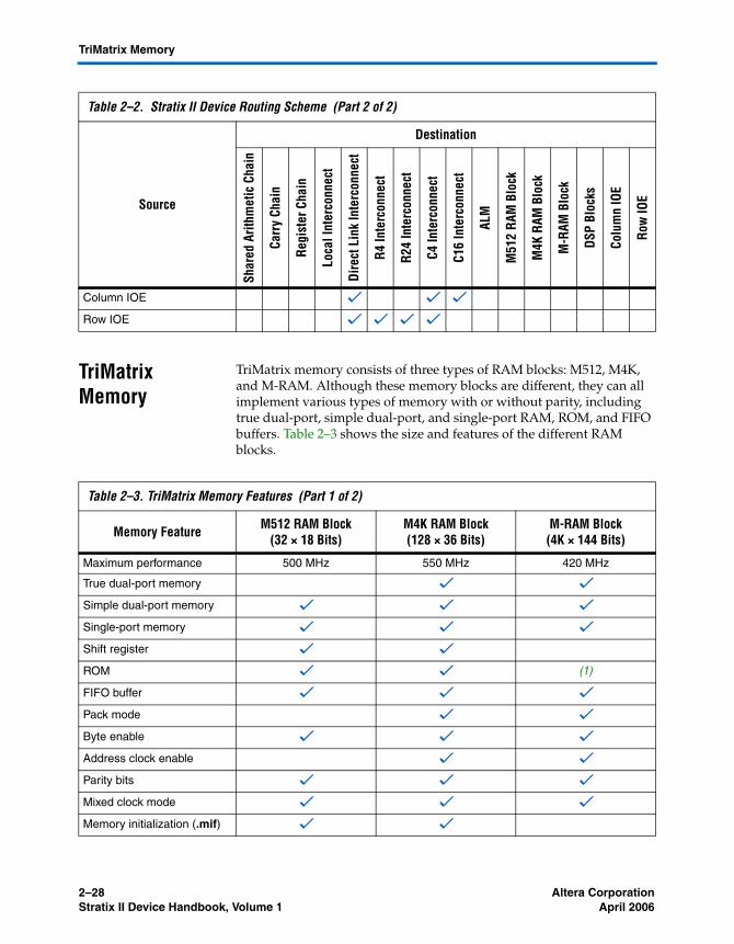
TriMatrix memory consists of three types of RAM blocks: M512, M4K, and M-RAM. Although these memory blocks are different, they can all implement various types of memory with or without parity, including true dual-port, simple dual-port, and single-port RAM, ROM, and FIFO buffers. Table 2–3 shows the size and features of the different RAM blocks.
Column IOE v v v
Row IOE v v v v
Table 2–2. Stratix II Device Routing Scheme (Part 2 of 2)
Source
Destination
Shar
ed A
rithm
etic
Cha
in
Carr
y Ch
ain
Regi
ster
Cha
in
Loca
l Int
erco
nnec
t
Dire
ct L
ink
Inte
rcon
nect
R4 In
terc
onne
ct
R24
Inte
rcon
nect
C4 In
terc
onne
ct
C16
Inte
rcon
nect
ALM
M51
2 RA
M B
lock
M4K
RAM
Blo
ck
M-R
AM B
lock
DSP
Bloc
ks
Colu
mn
IOE
Row
IOE
Table 2–3. TriMatrix Memory Features (Part 1 of 2)
Memory Feature M512 RAM Block (32 × 18 Bits)
M4K RAM Block (128 × 36 Bits)
M-RAM Block (4K × 144 Bits)
Maximum performance 500 MHz 550 MHz 420 MHz
True dual-port memory v v
Simple dual-port memory v v v
Single-port memory v v v
Shift register v v
ROM v v (1)
FIFO buffer v v v
Pack mode v v
Byte enable v v v
Address clock enable v v
Parity bits v v v
Mixed clock mode v v v
Memory initialization (.mif) v v
Altera Corporation 2–29April 2006 Stratix II Device Handbook, Volume 1
Stratix II Architecture
Memory Block Size
TriMatrix memory provides three different memory sizes for efficient application support. The Quartus II software automatically partitions the user-defined memory into the embedded memory blocks using the most efficient size combinations. You can also manually assign the memory to a specific block size or a mixture of block sizes.
When applied to input registers, the asynchronous clear signal for the TriMatrix embedded memory immediately clears the input registers. However, the output of the memory block does not show the effects until the next clock edge. When applied to output registers, the asynchronous clear signal clears the output registers and the effects are seen immediately.
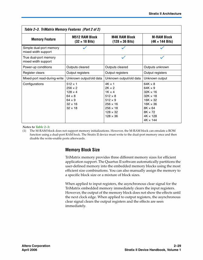
Simple dual-port memory mixed width support
v v v
True dual-port memory mixed width support
v v
Power-up conditions Outputs cleared Outputs cleared Outputs unknown
Register clears Output registers Output registers Output registers
Mixed-port read-during-write Unknown output/old data Unknown output/old data Unknown output
Configurations 512 × 1256 × 2128 × 464 × 864 × 932 × 1632 × 18
4K × 12K × 21K × 4512 × 8512 × 9256 × 16256 × 18128 × 32128 × 36
64K × 864K × 932K × 1632K × 1816K × 3216K × 368K × 648K × 724K × 1284K × 144
Notes to Table 2–3:(1) The M-RAM block does not support memory initializations. However, the M-RAM block can emulate a ROM
function using a dual-port RAM bock. The Stratix II device must write to the dual-port memory once and then disable the write-enable ports afterwards.
Table 2–3. TriMatrix Memory Features (Part 2 of 2)
Memory Feature M512 RAM Block (32 × 18 Bits)
M4K RAM Block (128 × 36 Bits)
M-RAM Block (4K × 144 Bits)
2–30 Altera CorporationStratix II Device Handbook, Volume 1 April 2006
TriMatrix Memory
M512 RAM Block
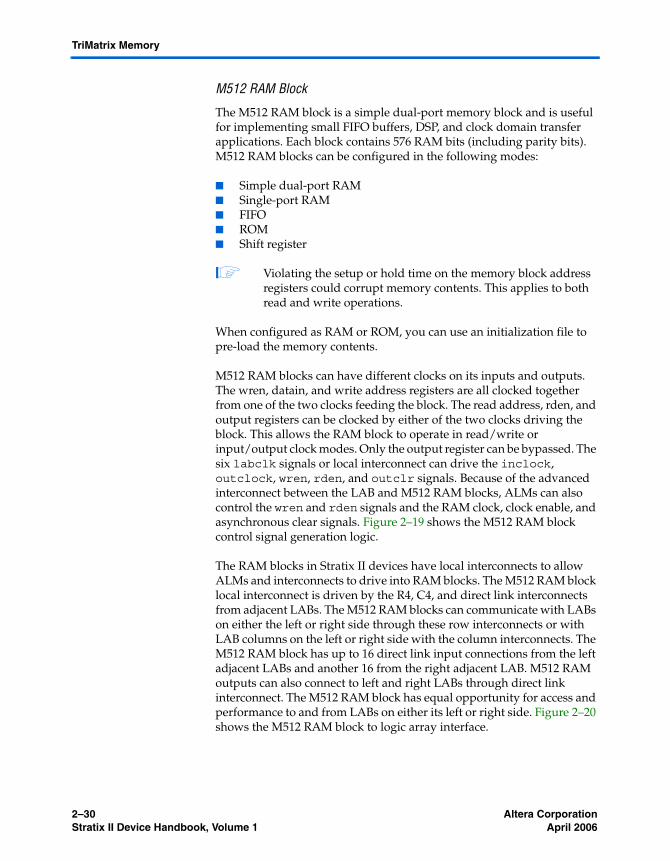
The M512 RAM block is a simple dual-port memory block and is useful for implementing small FIFO buffers, DSP, and clock domain transfer applications. Each block contains 576 RAM bits (including parity bits). M512 RAM blocks can be configured in the following modes:
■ Simple dual-port RAM■ Single-port RAM■ FIFO■ ROM■ Shift register
1 Violating the setup or hold time on the memory block address registers could corrupt memory contents. This applies to both read and write operations.
When configured as RAM or ROM, you can use an initialization file to pre-load the memory contents.
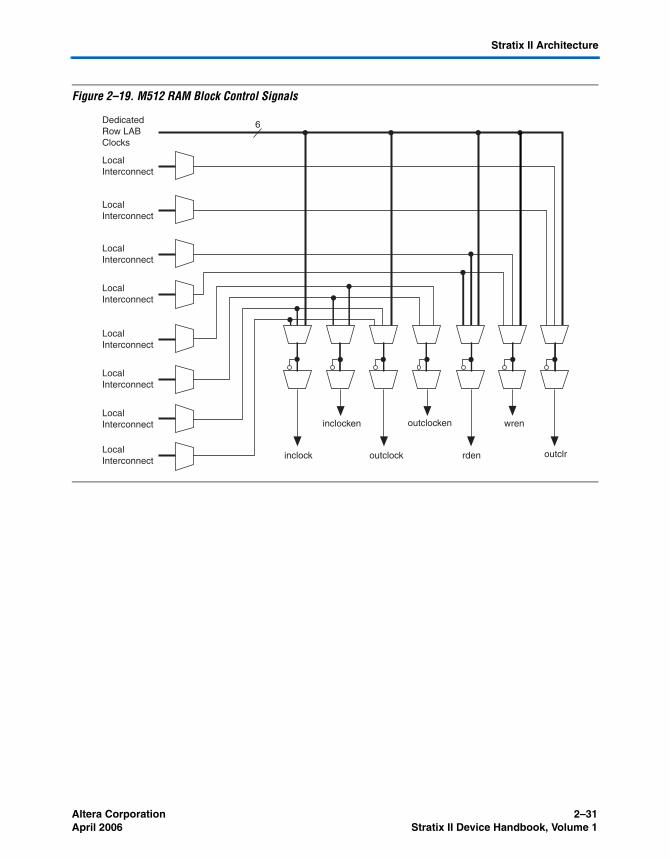
M512 RAM blocks can have different clocks on its inputs and outputs. The wren, datain, and write address registers are all clocked together from one of the two clocks feeding the block. The read address, rden, and output registers can be clocked by either of the two clocks driving the block. This allows the RAM block to operate in read/write or input/output clock modes. Only the output register can be bypassed. The six labclk signals or local interconnect can drive the inclock, outclock, wren, rden, and outclr signals. Because of the advanced interconnect between the LAB and M512 RAM blocks, ALMs can also control the wren and rden signals and the RAM clock, clock enable, and asynchronous clear signals. Figure 2–19 shows the M512 RAM block control signal generation logic.
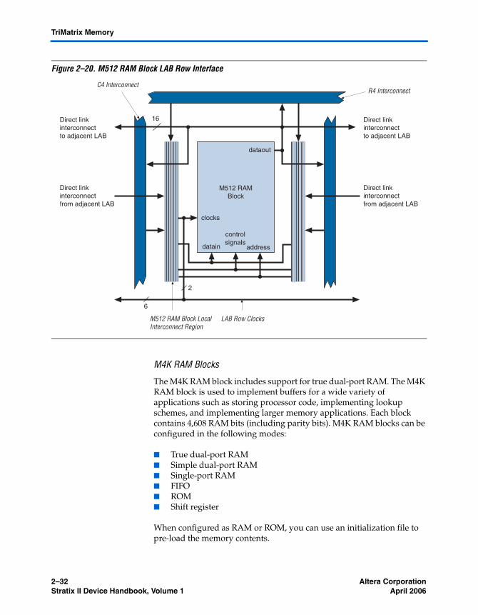
The RAM blocks in Stratix II devices have local interconnects to allow ALMs and interconnects to drive into RAM blocks. The M512 RAM block local interconnect is driven by the R4, C4, and direct link interconnects from adjacent LABs. The M512 RAM blocks can communicate with LABs on either the left or right side through these row interconnects or with LAB columns on the left or right side with the column interconnects. The M512 RAM block has up to 16 direct link input connections from the left adjacent LABs and another 16 from the right adjacent LAB. M512 RAM outputs can also connect to left and right LABs through direct link interconnect. The M512 RAM block has equal opportunity for access and performance to and from LABs on either its left or right side. Figure 2–20 shows the M512 RAM block to logic array interface.
Altera Corporation 2–31April 2006 Stratix II Device Handbook, Volume 1
Stratix II Architecture
Figure 2–19. M512 RAM Block Control Signals
inclocken
outclockinclock
outclocken
rden
wren
DedicatedRow LABClocks
LocalInterconnect
LocalInterconnect
LocalInterconnect
LocalInterconnect
LocalInterconnect
LocalInterconnect
outclr
6
LocalInterconnect
LocalInterconnect
2–32 Altera CorporationStratix II Device Handbook, Volume 1 April 2006
TriMatrix Memory
Figure 2–20. M512 RAM Block LAB Row Interface
M4K RAM Blocks
The M4K RAM block includes support for true dual-port RAM. The M4K RAM block is used to implement buffers for a wide variety of applications such as storing processor code, implementing lookup schemes, and implementing larger memory applications. Each block contains 4,608 RAM bits (including parity bits). M4K RAM blocks can be configured in the following modes:
■ True dual-port RAM■ Simple dual-port RAM■ Single-port RAM■ FIFO■ ROM■ Shift register
When configured as RAM or ROM, you can use an initialization file to pre-load the memory contents.
dataout
M512 RAMBlock
datain
clocks
16
Direct link interconnectfrom adjacent LAB
Direct link interconnectto adjacent LAB
Direct link interconnectfrom adjacent LAB
Direct link interconnectto adjacent LAB
M512 RAM Block LocalInterconnect Region
C4 InterconnectR4 Interconnect
controlsignals
address
LAB Row Clocks
2
6
Altera Corporation 2–33April 2006 Stratix II Device Handbook, Volume 1
Stratix II Architecture
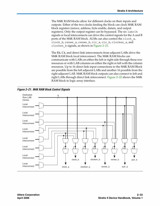
The M4K RAM blocks allow for different clocks on their inputs and outputs. Either of the two clocks feeding the block can clock M4K RAM block registers (renwe, address, byte enable, datain, and output registers). Only the output register can be bypassed. The six labclk signals or local interconnects can drive the control signals for the A and B ports of the M4K RAM block. ALMs can also control the clock_a, clock_b, renwe_a, renwe_b, clr_a, clr_b, clocken_a, and clocken_b signals, as shown in Figure 2–21.
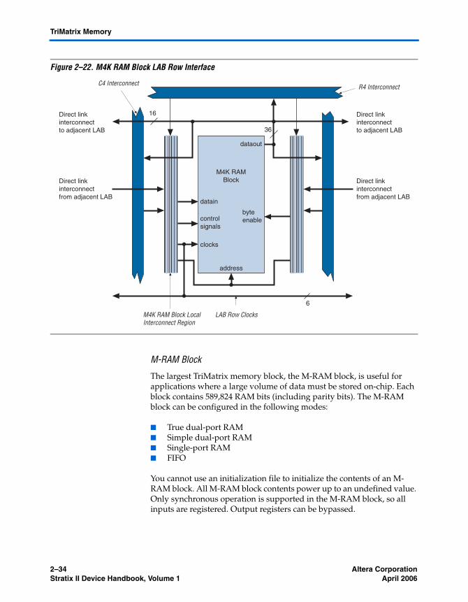
The R4, C4, and direct link interconnects from adjacent LABs drive the M4K RAM block local interconnect. The M4K RAM blocks can communicate with LABs on either the left or right side through these row resources or with LAB columns on either the right or left with the column resources. Up to 16 direct link input connections to the M4K RAM Block are possible from the left adjacent LABs and another 16 possible from the right adjacent LAB. M4K RAM block outputs can also connect to left and right LABs through direct link interconnect. Figure 2–22 shows the M4K RAM block to logic array interface.
Figure 2–21. M4K RAM Block Control Signals
clock_b
clocken_aclock_a
clocken_b aclr_b
aclr_a
DedicatedRow LABClocks
LocalInterconnect
LocalInterconnect
LocalInterconnect
LocalInterconnect
LocalInterconnect
LocalInterconnect
LocalInterconnect
LocalInterconnect
renwe_b
renwe_a
6
2–34 Altera CorporationStratix II Device Handbook, Volume 1 April 2006
TriMatrix Memory
Figure 2–22. M4K RAM Block LAB Row Interface
M-RAM Block
The largest TriMatrix memory block, the M-RAM block, is useful for applications where a large volume of data must be stored on-chip. Each block contains 589,824 RAM bits (including parity bits). The M-RAM block can be configured in the following modes:
■ True dual-port RAM■ Simple dual-port RAM■ Single-port RAM■ FIFO
You cannot use an initialization file to initialize the contents of an M-RAM block. All M-RAM block contents power up to an undefined value. Only synchronous operation is supported in the M-RAM block, so all inputs are registered. Output registers can be bypassed.
dataout
M4K RAMBlock
datain
address
16
36
Direct link interconnectfrom adjacent LAB
Direct link interconnectto adjacent LAB
Direct link interconnectfrom adjacent LAB
Direct link interconnectto adjacent LAB
M4K RAM Block LocalInterconnect Region
C4 Interconnect R4 Interconnect
LAB Row Clocks
clocks
byteenablecontrol
signals
6
Altera Corporation 2–35April 2006 Stratix II Device Handbook, Volume 1
Stratix II Architecture
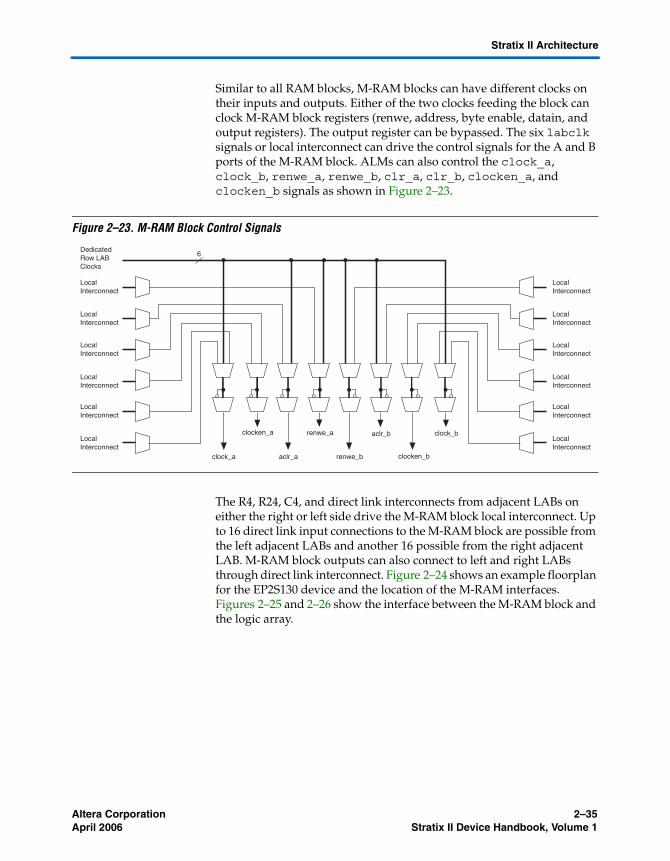
Similar to all RAM blocks, M-RAM blocks can have different clocks on their inputs and outputs. Either of the two clocks feeding the block can clock M-RAM block registers (renwe, address, byte enable, datain, and output registers). The output register can be bypassed. The six labclk signals or local interconnect can drive the control signals for the A and B ports of the M-RAM block. ALMs can also control the clock_a, clock_b, renwe_a, renwe_b, clr_a, clr_b, clocken_a, and clocken_b signals as shown in Figure 2–23.
Figure 2–23. M-RAM Block Control Signals
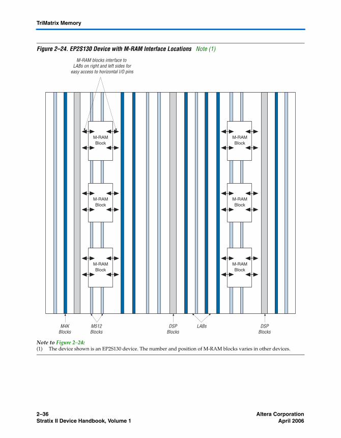
The R4, R24, C4, and direct link interconnects from adjacent LABs on either the right or left side drive the M-RAM block local interconnect. Up to 16 direct link input connections to the M-RAM block are possible from the left adjacent LABs and another 16 possible from the right adjacent LAB. M-RAM block outputs can also connect to left and right LABs through direct link interconnect. Figure 2–24 shows an example floorplan for the EP2S130 device and the location of the M-RAM interfaces. Figures 2–25 and 2–26 show the interface between the M-RAM block and the logic array.
clock_a
clock_bclocken_a
clocken_baclr_a
aclr_b
DedicatedRow LABClocks
LocalInterconnect
LocalInterconnect
LocalInterconnect
LocalInterconnect
renwe_a
renwe_b
6
LocalInterconnect
LocalInterconnect
LocalInterconnect
LocalInterconnect
LocalInterconnect
LocalInterconnect
LocalInterconnect
LocalInterconnect
2–36 Altera CorporationStratix II Device Handbook, Volume 1 April 2006
TriMatrix Memory
Figure 2–24. EP2S130 Device with M-RAM Interface Locations Note (1)
Note to Figure 2–24:(1) The device shown is an EP2S130 device. The number and position of M-RAM blocks varies in other devices.
DSPBlocks
DSPBlocks
M4KBlocks
M512Blocks
LABs
M-RAMBlock
M-RAMBlock
M-RAMBlock
M-RAMBlock
M-RAMBlock
M-RAMBlock
M-RAM blocks interface to LABs on right and left sides for
easy access to horizontal I/O pins
Altera Corporation 2–37April 2006 Stratix II Device Handbook, Volume 1
Stratix II Architecture
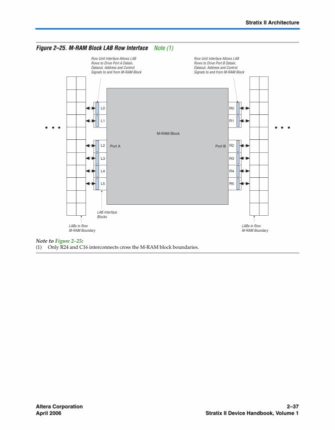
Figure 2–25. M-RAM Block LAB Row Interface Note (1)
Note to Figure 2–25:(1) Only R24 and C16 interconnects cross the M-RAM block boundaries.
M-RAM Block
Port BPort A
Row Unit Interface Allows LABRows to Drive Port B Datain,Dataout, Address and ControlSignals to and from M-RAM Block
Row Unit Interface Allows LABRows to Drive Port A Datain,Dataout, Address and ControlSignals to and from M-RAM Block
LABs in RowM-RAM Boundary
LABs in RowM-RAM Boundary
LAB InterfaceBlocks
L0
L1
L2
L3
L4
L5
R0
R1
R2
R3
R4
R5
2–38 Altera CorporationStratix II Device Handbook, Volume 1 April 2006
TriMatrix Memory
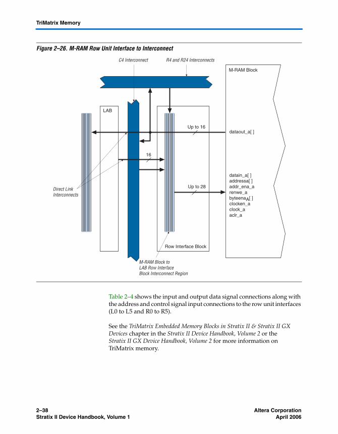
Figure 2–26. M-RAM Row Unit Interface to Interconnect
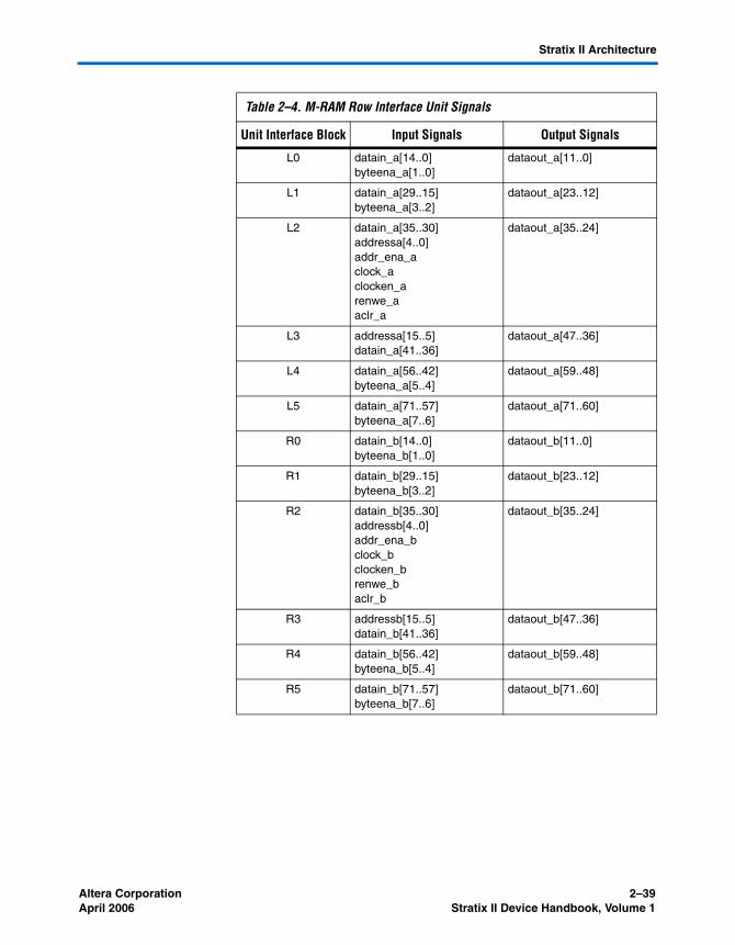
Table 2–4 shows the input and output data signal connections along with the address and control signal input connections to the row unit interfaces (L0 to L5 and R0 to R5).
See the TriMatrix Embedded Memory Blocks in Stratix II & Stratix II GX Devices chapter in the Stratix II Device Handbook, Volume 2 or the Stratix II GX Device Handbook, Volume 2 for more information on TriMatrix memory.
LAB
Row Interface Block
M-RAM Block
16
Up to 28
datain_a[ ]addressa[ ]addr_ena_arenwe_abyteenaA[ ]clocken_aclock_aaclr_a
M-RAM Block toLAB Row InterfaceBlock Interconnect Region
R4 and R24 InterconnectsC4 Interconnect
Direct LinkInterconnects
dataout_a[ ]Up to 16
Altera Corporation 2–39April 2006 Stratix II Device Handbook, Volume 1
Stratix II Architecture
Table 2–4. M-RAM Row Interface Unit Signals
Unit Interface Block Input Signals Output Signals
L0 datain_a[14..0]byteena_a[1..0]
dataout_a[11..0]
L1 datain_a[29..15]byteena_a[3..2]
dataout_a[23..12]
L2 datain_a[35..30]addressa[4..0]addr_ena_aclock_aclocken_arenwe_aaclr_a
dataout_a[35..24]
L3 addressa[15..5]datain_a[41..36]
dataout_a[47..36]
L4 datain_a[56..42]byteena_a[5..4]
dataout_a[59..48]
L5 datain_a[71..57]byteena_a[7..6]
dataout_a[71..60]
R0 datain_b[14..0]byteena_b[1..0]
dataout_b[11..0]
R1 datain_b[29..15]byteena_b[3..2]
dataout_b[23..12]
R2 datain_b[35..30]addressb[4..0]addr_ena_bclock_bclocken_brenwe_baclr_b
dataout_b[35..24]
R3 addressb[15..5]datain_b[41..36]
dataout_b[47..36]
R4 datain_b[56..42]byteena_b[5..4]
dataout_b[59..48]
R5 datain_b[71..57]byteena_b[7..6]
dataout_b[71..60]
2–40 Altera CorporationStratix II Device Handbook, Volume 1 April 2006
Digital Signal Processing Block
Digital Signal Processing Block
The most commonly used DSP functions are FIR filters, complex FIR filters, IIR filters, fast Fourier transform (FFT) functions, direct cosine transform (DCT) functions, and correlators. All of these use the multiplier as the fundamental building block. Additionally, some applications need specialized operations such as multiply-add and multiply-accumulate operations. Stratix II devices provide DSP blocks to meet the arithmetic requirements of these functions.
Each Stratix II device has from two to four columns of DSP blocks to efficiently implement DSP functions faster than ALM-based implementations. Stratix II devices have up to 24 DSP blocks per column (see Table 2–5). Each DSP block can be configured to support up to:
■ Eight 9 × 9-bit multipliers■ Four 18 × 18-bit multipliers■ One 36 × 36-bit multiplier
As indicated, the Stratix II DSP block can support one 36 × 36-bit multiplier in a single DSP block. This is true for any combination of signed, unsigned, or mixed sign multiplications.
1 This list only shows functions that can fit into a single DSP block. Multiple DSP blocks can support larger multiplication functions.
Figure 2–27 shows one of the columns with surrounding LAB rows.
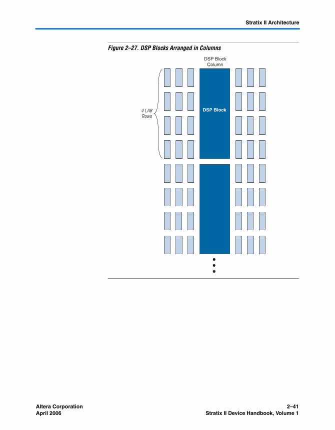
Altera Corporation 2–41April 2006 Stratix II Device Handbook, Volume 1
Stratix II Architecture
Figure 2–27. DSP Blocks Arranged in Columns
DSP BlockColumn
4 LABRows
DSP Block
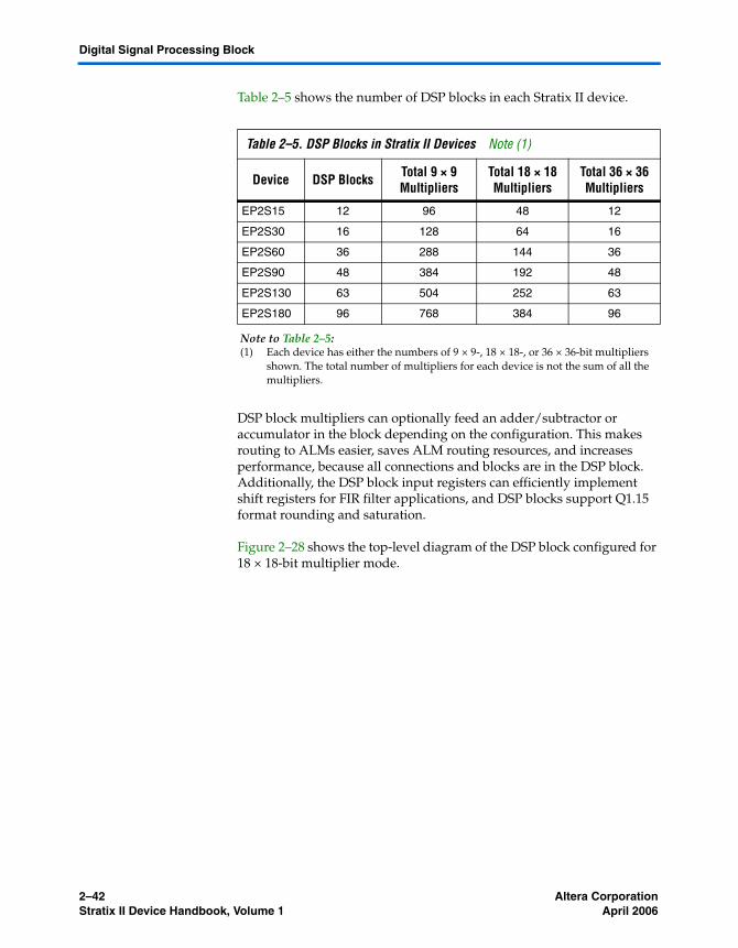
2–42 Altera CorporationStratix II Device Handbook, Volume 1 April 2006
Digital Signal Processing Block
Table 2–5 shows the number of DSP blocks in each Stratix II device.
DSP block multipliers can optionally feed an adder/subtractor or accumulator in the block depending on the configuration. This makes routing to ALMs easier, saves ALM routing resources, and increases performance, because all connections and blocks are in the DSP block. Additionally, the DSP block input registers can efficiently implement shift registers for FIR filter applications, and DSP blocks support Q1.15 format rounding and saturation.
Figure 2–28 shows the top-level diagram of the DSP block configured for 18 × 18-bit multiplier mode.
Table 2–5. DSP Blocks in Stratix II Devices Note (1)
Device DSP Blocks Total 9 × 9 Multipliers
Total 18 × 18 Multipliers
Total 36 × 36 Multipliers
EP2S15 12 96 48 12
EP2S30 16 128 64 16
EP2S60 36 288 144 36
EP2S90 48 384 192 48
EP2S130 63 504 252 63
EP2S180 96 768 384 96
Note to Table 2–5:(1) Each device has either the numbers of 9 × 9-, 18 × 18-, or 36 × 36-bit multipliers
shown. The total number of multipliers for each device is not the sum of all the multipliers.
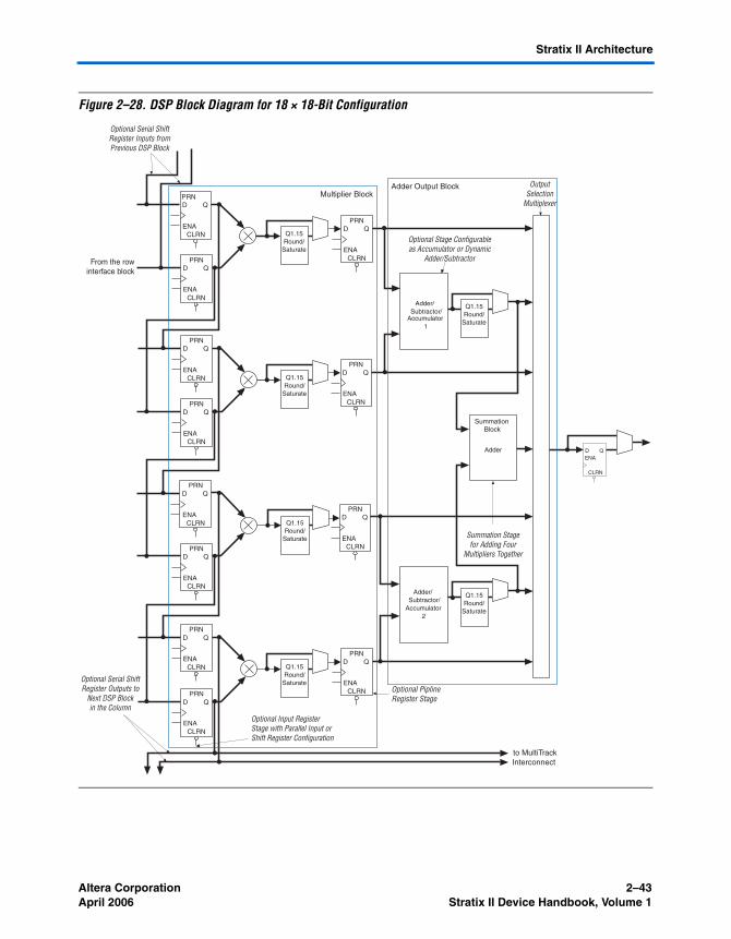
Altera Corporation 2–43April 2006 Stratix II Device Handbook, Volume 1
Stratix II Architecture
Figure 2–28. DSP Block Diagram for 18 × 18-Bit Configuration
Adder/Subtractor/
Accumulator1
Adder
Multiplier BlockPRN
CLRN
D Q
ENA
PRN
CLRN
D Q
ENA
PRN
CLRN
D Q
ENA
PRN
CLRN
D Q
ENA
PRN
CLRN
D Q
ENA
PRN
CLRN
D Q
ENA
PRN
CLRN
D Q
ENA
PRN
CLRN
D Q
ENA
PRN
CLRN
D Q
ENA
PRN
CLRN
D Q
ENA
PRN
CLRN
D Q
ENA
PRN
CLRN
D Q
ENA
SummationBlock
Adder Output Block
Adder/Subtractor/
Accumulator2
Q1.15Round/
Saturate
Q1.15Round/
Saturate
Q1.15Round/
Saturate
Q1.15Round/
Saturate
to MultiTrackInterconnect
CLRN
D QENA
From the rowinterface block
Optional Serial ShiftRegister Inputs fromPrevious DSP Block
Optional Serial ShiftRegister Outputs to
Next DSP Blockin the Column
Optional Input RegisterStage with Parallel Input orShift Register Configuration
Optional PiplineRegister Stage
Summation Stagefor Adding Four
Multipliers Together
Optional Stage Configurableas Accumulator or Dynamic
Adder/Subtractor
OutputSelection
Multiplexer
Q1.15Round/
Saturate
Q1.15Round/
Saturate
2–44 Altera CorporationStratix II Device Handbook, Volume 1 April 2006
Digital Signal Processing Block
Modes of Operation
The adder, subtractor, and accumulate functions of a DSP block have four modes of operation:
■ Simple multiplier■ Multiply-accumulator■ Two-multipliers adder■ Four-multipliers adder
Table 2–6 shows the different number of multipliers possible in each DSP block mode according to size. These modes allow the DSP blocks to implement numerous applications for DSP including FFTs, complex FIR, FIR, and 2D FIR filters, equalizers, IIR, correlators, matrix multiplication and many other functions. The DSP blocks also support mixed modes and mixed multiplier sizes in the same block. For example, half of one DSP block can implement one 18 × 18-bit multiplier in multiply-accumulator mode, while the other half of the DSP block implements four 9 × 9-bit multipliers in simple multiplier mode.
DSP Block Interface
Stratix II device DSP block input registers can generate a shift register that can cascade down in the same DSP block column. Dedicated connections between DSP blocks provide fast connections between the shift register inputs to cascade the shift register chains. You can cascade registers within multiple DSP blocks for 9 × 9- or 18 × 18-bit FIR filters larger than four taps, with additional adder stages implemented in ALMs. If the DSP block is configured as 36 × 36 bits, the adder, subtractor, or accumulator stages are implemented in ALMs. Each DSP block can route the shift register chain out of the block to cascade multiple columns of DSP blocks.
Table 2–6. Multiplier Size & Configurations per DSP Block
DSP Block Mode 9 × 9 18 × 18 36 × 36
Multiplier Eight multipliers with eight product outputs
Four multipliers with four product outputs
One multiplier with one product output
Multiply-accumulator - Two 52-bit multiply-accumulate blocks
-
Two-multipliers adder Four two-multiplier adder (two 9 × 9 complex multiply)
Two two-multiplier adder (one 18 × 18 complex multiply)
-
Four-multipliers adder Two four-multiplier adder One four-multiplier adder -
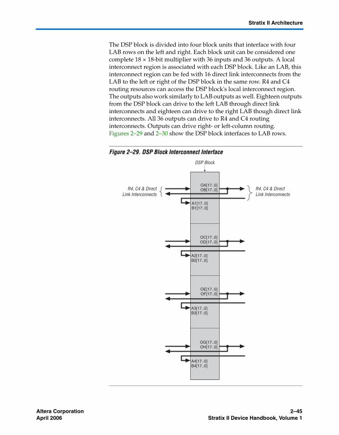
Altera Corporation 2–45April 2006 Stratix II Device Handbook, Volume 1
Stratix II Architecture
The DSP block is divided into four block units that interface with four LAB rows on the left and right. Each block unit can be considered one complete 18 × 18-bit multiplier with 36 inputs and 36 outputs. A local interconnect region is associated with each DSP block. Like an LAB, this interconnect region can be fed with 16 direct link interconnects from the LAB to the left or right of the DSP block in the same row. R4 and C4 routing resources can access the DSP block's local interconnect region. The outputs also work similarly to LAB outputs as well. Eighteen outputs from the DSP block can drive to the left LAB through direct link interconnects and eighteen can drive to the right LAB though direct link interconnects. All 36 outputs can drive to R4 and C4 routing interconnects. Outputs can drive right- or left-column routing. Figures 2–29 and 2–30 show the DSP block interfaces to LAB rows.
Figure 2–29. DSP Block Interconnect Interface
A1[17..0]B1[17..0]
A2[17..0]B2[17..0]
A3[17..0]B3[17..0]
A4[17..0]B4[17..0]
OA[17..0]OB[17..0]
OC[17..0]OD[17..0]
OE[17..0]OF[17..0]
OG[17..0]OH[17..0]
DSP Block
R4, C4 & DirectLink Interconnects
R4, C4 & DirectLink Interconnects
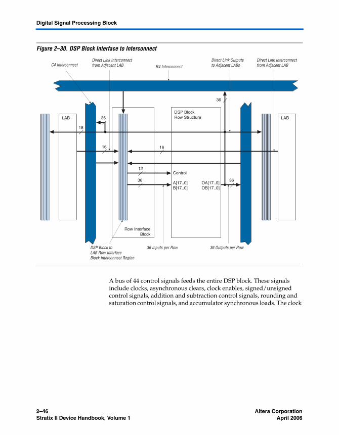
2–46 Altera CorporationStratix II Device Handbook, Volume 1 April 2006
Digital Signal Processing Block
Figure 2–30. DSP Block Interface to Interconnect
A bus of 44 control signals feeds the entire DSP block. These signals include clocks, asynchronous clears, clock enables, signed/unsigned control signals, addition and subtraction control signals, rounding and saturation control signals, and accumulator synchronous loads. The clock
LAB LAB
Row InterfaceBlock
DSP BlockRow Structure
16
OA[17..0]OB[17..0]
A[17..0]B[17..0]
DSP Block toLAB Row InterfaceBlock Interconnect Region
36 Inputs per Row 36 Outputs per Row
R4 InterconnectC4 InterconnectDirect Link Interconnectfrom Adjacent LAB
Direct Link Outputsto Adjacent LABs
Direct Link Interconnectfrom Adjacent LAB
36
36
36
36
Control12
16
18
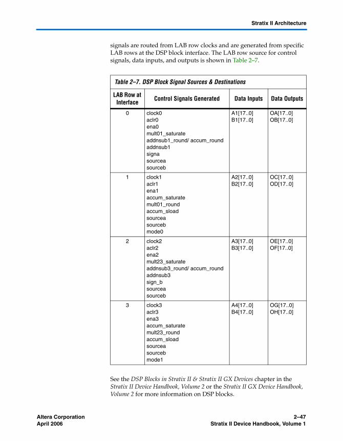
Altera Corporation 2–47April 2006 Stratix II Device Handbook, Volume 1
Stratix II Architecture
signals are routed from LAB row clocks and are generated from specific LAB rows at the DSP block interface. The LAB row source for control signals, data inputs, and outputs is shown in Table 2–7.
See the DSP Blocks in Stratix II & Stratix II GX Devices chapter in the Stratix II Device Handbook, Volume 2 or the Stratix II GX Device Handbook, Volume 2 for more information on DSP blocks.
Table 2–7. DSP Block Signal Sources & Destinations
LAB Row at Interface Control Signals Generated Data Inputs Data Outputs
0 clock0aclr0ena0mult01_saturateaddnsub1_round/ accum_roundaddnsub1signasourceasourceb
A1[17..0]B1[17..0]
OA[17..0]OB[17..0]
1 clock1aclr1ena1accum_saturatemult01_roundaccum_sloadsourceasourcebmode0
A2[17..0]B2[17..0]
OC[17..0]OD[17..0]
2 clock2aclr2ena2mult23_saturateaddnsub3_round/ accum_roundaddnsub3sign_bsourceasourceb
A3[17..0]B3[17..0]
OE[17..0]OF[17..0]
3 clock3aclr3ena3accum_saturatemult23_roundaccum_sloadsourceasourcebmode1
A4[17..0]B4[17..0]
OG[17..0]OH[17..0]
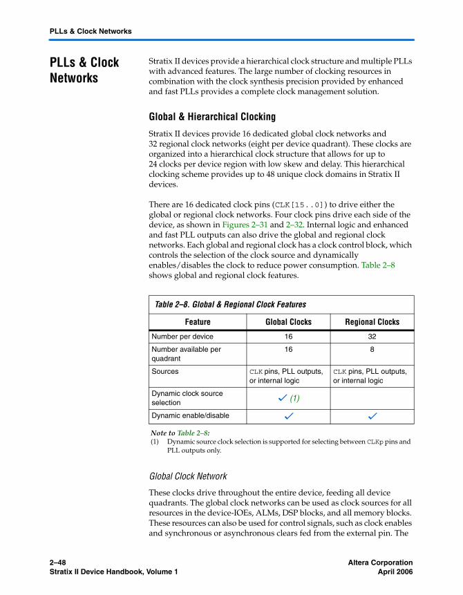
2–48 Altera CorporationStratix II Device Handbook, Volume 1 April 2006
PLLs & Clock Networks
PLLs & Clock Networks
Stratix II devices provide a hierarchical clock structure and multiple PLLs with advanced features. The large number of clocking resources in combination with the clock synthesis precision provided by enhanced and fast PLLs provides a complete clock management solution.
Global & Hierarchical Clocking
Stratix II devices provide 16 dedicated global clock networks and 32 regional clock networks (eight per device quadrant). These clocks are organized into a hierarchical clock structure that allows for up to 24 clocks per device region with low skew and delay. This hierarchical clocking scheme provides up to 48 unique clock domains in Stratix II devices.
There are 16 dedicated clock pins (CLK[15..0]) to drive either the global or regional clock networks. Four clock pins drive each side of the device, as shown in Figures 2–31 and 2–32. Internal logic and enhanced and fast PLL outputs can also drive the global and regional clock networks. Each global and regional clock has a clock control block, which controls the selection of the clock source and dynamically enables/disables the clock to reduce power consumption. Table 2–8 shows global and regional clock features.
Global Clock Network
These clocks drive throughout the entire device, feeding all device quadrants. The global clock networks can be used as clock sources for all resources in the device-IOEs, ALMs, DSP blocks, and all memory blocks. These resources can also be used for control signals, such as clock enables and synchronous or asynchronous clears fed from the external pin. The
Table 2–8. Global & Regional Clock Features
Feature Global Clocks Regional Clocks
Number per device 16 32
Number available per quadrant
16 8
Sources CLK pins, PLL outputs, or internal logic
CLK pins, PLL outputs, or internal logic
Dynamic clock source selection v (1)
Dynamic enable/disable v v
Note to Table 2–8:(1) Dynamic source clock selection is supported for selecting between CLKp pins and
PLL outputs only.
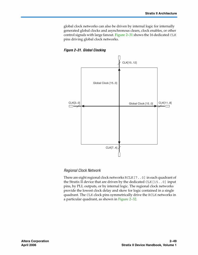
Altera Corporation 2–49April 2006 Stratix II Device Handbook, Volume 1
Stratix II Architecture
global clock networks can also be driven by internal logic for internally generated global clocks and asynchronous clears, clock enables, or other control signals with large fanout. Figure 2–31 shows the 16 dedicated CLK pins driving global clock networks.
Figure 2–31. Global Clocking
Regional Clock Network
There are eight regional clock networks RCLK[7..0] in each quadrant of the Stratix II device that are driven by the dedicated CLK[15..0] input pins, by PLL outputs, or by internal logic. The regional clock networks provide the lowest clock delay and skew for logic contained in a single quadrant. The CLK clock pins symmetrically drive the RCLK networks in a particular quadrant, as shown in Figure 2–32.
Global Clock [15..0]
CLK[15..12]
CLK[3..0]
CLK[7..4]
CLK[11..8] Global Clock [15..0]
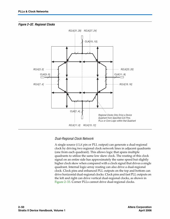
2–50 Altera CorporationStratix II Device Handbook, Volume 1 April 2006
PLLs & Clock Networks
Figure 2–32. Regional Clocks
Dual-Regional Clock Network
A single source (CLK pin or PLL output) can generate a dual-regional clock by driving two regional clock network lines in adjacent quadrants (one from each quadrant). This allows logic that spans multiple quadrants to utilize the same low skew clock. The routing of this clock signal on an entire side has approximately the same speed but slightly higher clock skew when compared with a clock signal that drives a single quadrant. Internal logic-array routing can also drive a dual-regional clock. Clock pins and enhanced PLL outputs on the top and bottom can drive horizontal dual-regional clocks. Clock pins and fast PLL outputs on the left and right can drive vertical dual-regional clocks, as shown in Figure 2–33. Corner PLLs cannot drive dual-regional clocks.
RCLK[3..0]
RCLK[7..4]
RCLK[11..8] RCLK[15..12]
RCLK[31..28] RCLK[27..24]
RCLK[19..16]
RCLK[23..20]
CLK[15..12]
CLK[3..0]
CLK[7..4]
CLK[11..8]
Regional Clocks Only Drive a Device Quadrant from Specified CLK Pins, PLLs or Core Logic within that Quadrant
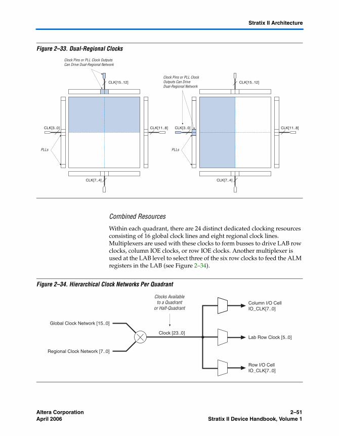
Altera Corporation 2–51April 2006 Stratix II Device Handbook, Volume 1
Stratix II Architecture
Figure 2–33. Dual-Regional Clocks
Combined Resources
Within each quadrant, there are 24 distinct dedicated clocking resources consisting of 16 global clock lines and eight regional clock lines. Multiplexers are used with these clocks to form busses to drive LAB row clocks, column IOE clocks, or row IOE clocks. Another multiplexer is used at the LAB level to select three of the six row clocks to feed the ALM registers in the LAB (see Figure 2–34).
Figure 2–34. Hierarchical Clock Networks Per Quadrant
Clock Pins or PLL Clock OutputsCan Drive Dual-Regional Network
CLK[15..12]
CLK[11..8]
CLK[7..4]
CLK[3..0]
PLLsPLLs
Clock Pins or PLL ClockOutputs Can DriveDual-Regional Network
CLK[15..12]
CLK[11..8]
CLK[7..4]
CLK[3..0]
Clock [23..0]
Column I/O CellIO_CLK[7..0]
Lab Row Clock [5..0]
Row I/O CellIO_CLK[7..0]
Global Clock Network [15..0]
Regional Clock Network [7..0]
Clocks Availableto a Quadrant
or Half-Quadrant
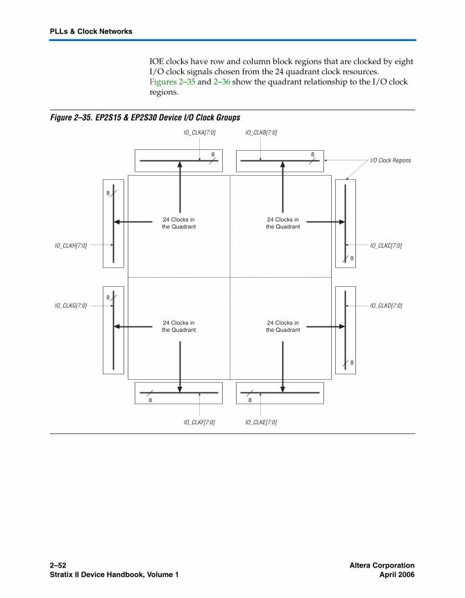
2–52 Altera CorporationStratix II Device Handbook, Volume 1 April 2006
PLLs & Clock Networks
IOE clocks have row and column block regions that are clocked by eight I/O clock signals chosen from the 24 quadrant clock resources. Figures 2–35 and 2–36 show the quadrant relationship to the I/O clock regions.
Figure 2–35. EP2S15 & EP2S30 Device I/O Clock Groups
IO_CLKC[7:0]
IO_CLKF[7:0] IO_CLKE[7:0]
IO_CLKA[7:0] IO_CLKB[7:0]
IO_CLKD[7:0]
IO_CLKH[7:0]
IO_CLKG[7:0]
8
8
24 Clocks inthe Quadrant
24 Clocks inthe Quadrant
24 Clocks inthe Quadrant
24 Clocks inthe Quadrant
8
8
8
8
8 8I/O Clock Regions
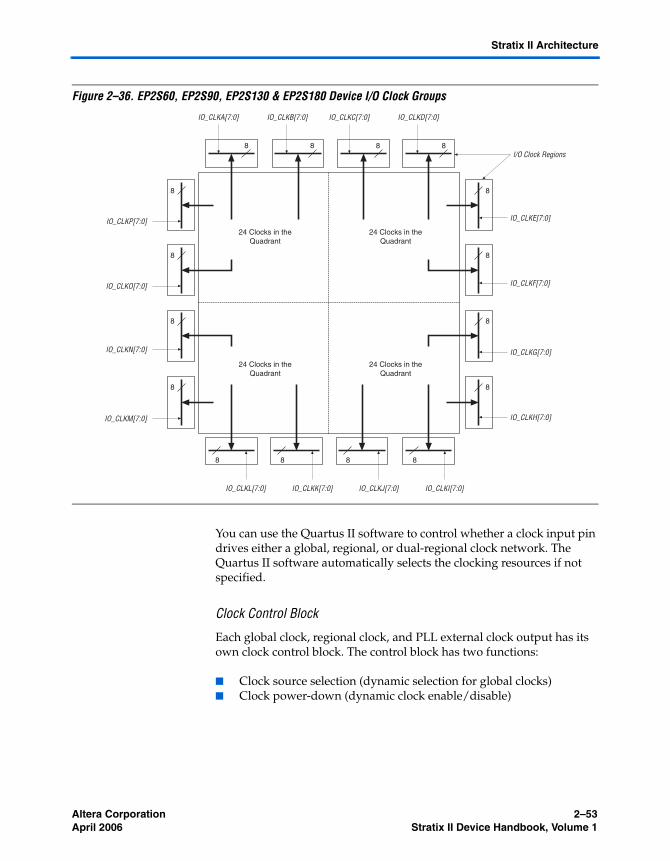
Altera Corporation 2–53April 2006 Stratix II Device Handbook, Volume 1
Stratix II Architecture
Figure 2–36. EP2S60, EP2S90, EP2S130 & EP2S180 Device I/O Clock Groups
You can use the Quartus II software to control whether a clock input pin drives either a global, regional, or dual-regional clock network. The Quartus II software automatically selects the clocking resources if not specified.
Clock Control Block
Each global clock, regional clock, and PLL external clock output has its own clock control block. The control block has two functions:
■ Clock source selection (dynamic selection for global clocks)■ Clock power-down (dynamic clock enable/disable)
IO_CLKJ[7:0] IO_CLKI[7:0]
IO_CLKA[7:0] IO_CLKB[7:0]
8
24 Clocks in theQuadrant
24 Clocks in theQuadrant
24 Clocks in theQuadrant
24 Clocks in theQuadrant
8 8 8
I/O Clock Regions
IO_CLKL[7:0] IO_CLKK[7:0]
IO_CLKC[7:0] IO_CLKD[7:0]
8 8 8 8
8
8
8
8
8
8
8
8
IO_CLKE[7:0]
IO_CLKF[7:0]
IO_CLKG[7:0]
IO_CLKH[7:0]
IO_CLKN[7:0]
IO_CLKM[7:0]
IO_CLKP[7:0]
IO_CLKO[7:0]
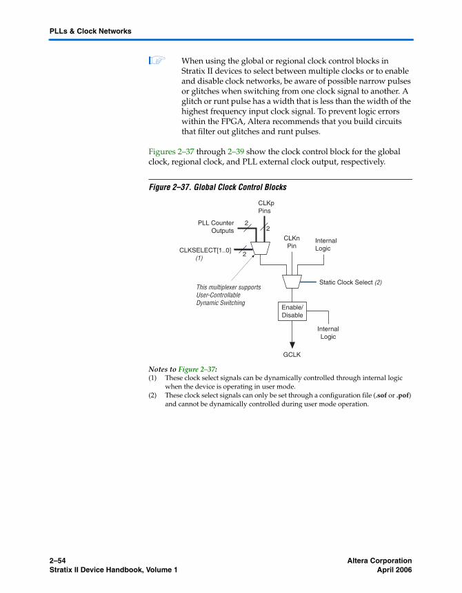
2–54 Altera CorporationStratix II Device Handbook, Volume 1 April 2006
PLLs & Clock Networks
1 When using the global or regional clock control blocks in Stratix II devices to select between multiple clocks or to enable and disable clock networks, be aware of possible narrow pulses or glitches when switching from one clock signal to another. A glitch or runt pulse has a width that is less than the width of the highest frequency input clock signal. To prevent logic errors within the FPGA, Altera recommends that you build circuits that filter out glitches and runt pulses.
Figures 2–37 through 2–39 show the clock control block for the global clock, regional clock, and PLL external clock output, respectively.
Figure 2–37. Global Clock Control Blocks
Notes to Figure 2–37:(1) These clock select signals can be dynamically controlled through internal logic
when the device is operating in user mode.(2) These clock select signals can only be set through a configuration file (.sof or .pof)
and cannot be dynamically controlled during user mode operation.
CLKpPins
PLL CounterOutputs
InternalLogic
CLKnPin
Enable/Disable
GCLK
InternalLogic
Static Clock SelectThis multiplexer supportsUser-ControllableDynamic Switching
CLKSELECT[1..0](1)
(2)
2
22
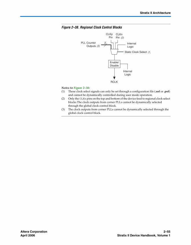
Altera Corporation 2–55April 2006 Stratix II Device Handbook, Volume 1
Stratix II Architecture
Figure 2–38. Regional Clock Control Blocks
Notes to Figure 2–38:(1) These clock select signals can only be set through a configuration file (.sof or .pof)
and cannot be dynamically controlled during user mode operation.(2) Only the CLKn pins on the top and bottom of the device feed to regional clock select
blocks.The clock outputs from corner PLLs cannot be dynamically selected through the global clock control block.
(3) The clock outputs from corner PLLs cannot be dynamically selected through the global clock control block.
CLKpPin
PLL CounterOutputs
InternalLogic
CLKnPin
Enable/Disable
RCLK
InternalLogic
Static Clock Select (1)
2
(2)
(3)
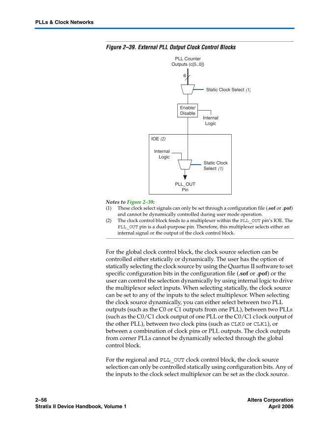
2–56 Altera CorporationStratix II Device Handbook, Volume 1 April 2006
PLLs & Clock Networks
Figure 2–39. External PLL Output Clock Control Blocks
Notes to Figure 2–39:(1) These clock select signals can only be set through a configuration file (.sof or .pof)
and cannot be dynamically controlled during user mode operation.(2) The clock control block feeds to a multiplexer within the PLL_OUT pin’s IOE. The
PLL_OUT pin is a dual-purpose pin. Therefore, this multiplexer selects either an internal signal or the output of the clock control block.
For the global clock control block, the clock source selection can be controlled either statically or dynamically. The user has the option of statically selecting the clock source by using the Quartus II software to set specific configuration bits in the configuration file (.sof or .pof) or the user can control the selection dynamically by using internal logic to drive the multiplexor select inputs. When selecting statically, the clock source can be set to any of the inputs to the select multiplexor. When selecting the clock source dynamically, you can either select between two PLL outputs (such as the C0 or C1 outputs from one PLL), between two PLLs (such as the C0/C1 clock output of one PLL or the C0/C1 c1ock output of the other PLL), between two clock pins (such as CLK0 or CLK1), or between a combination of clock pins or PLL outputs. The clock outputs from corner PLLs cannot be dynamically selected through the global control block.
For the regional and PLL_OUT clock control block, the clock source selection can only be controlled statically using configuration bits. Any of the inputs to the clock select multiplexor can be set as the clock source.
PLL CounterOutputs (c[5..0])
Enable/Disable
PLL_OUTPin
InternalLogic
Static Clock Select
IOE
(1)
Static ClockSelect (1)
6
InternalLogic
(2)
Altera Corporation 2–57April 2006 Stratix II Device Handbook, Volume 1
Stratix II Architecture
The Stratix II clock networks can be disabled (powered down) by both static and dynamic approaches. When a clock net is powered down, all the logic fed by the clock net is in an off-state thereby reducing the overall power consumption of the device.
The global and regional clock networks can be powered down statically through a setting in the configuration (.sof or .pof) file. Clock networks that are not used are automatically powered down through configuration bit settings in the configuration file generated by the Quartus II software.
The dynamic clock enable/disable feature allows the internal logic to control power up/down synchronously on GCLK and RCLK nets and PLL_OUT pins. This function is independent of the PLL and is applied directly on the clock network or PLL_OUT pin, as shown in Figures 2–37 through 2–39.
Enhanced & Fast PLLs
Stratix II devices provide robust clock management and synthesis using up to four enhanced PLLs and eight fast PLLs. These PLLs increase performance and provide advanced clock interfacing and clock-frequency synthesis. With features such as clock switchover, spread-spectrum clocking, reconfigurable bandwidth, phase control, and reconfigurable phase shifting, the Stratix II device’s enhanced PLLs provide you with complete control of clocks and system timing. The fast PLLs provide general purpose clocking with multiplication and phase shifting as well as high-speed outputs for high-speed differential I/O support. Enhanced and fast PLLs work together with the Stratix II high-speed I/O and advanced clock architecture to provide significant improvements in system performance and bandwidth.
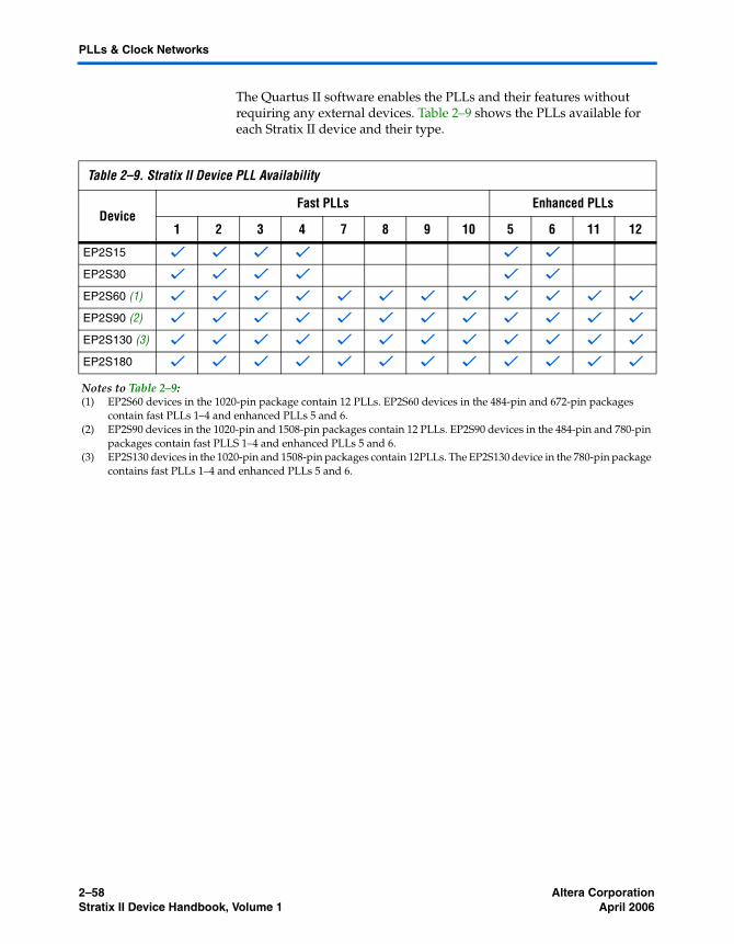
2–58 Altera CorporationStratix II Device Handbook, Volume 1 April 2006
PLLs & Clock Networks
The Quartus II software enables the PLLs and their features without requiring any external devices. Table 2–9 shows the PLLs available for each Stratix II device and their type.
Table 2–9. Stratix II Device PLL Availability
DeviceFast PLLs Enhanced PLLs
1 2 3 4 7 8 9 10 5 6 11 12
EP2S15 v v v v v v
EP2S30 v v v v v v
EP2S60 (1) v v v v v v v v v v v v
EP2S90 (2) v v v v v v v v v v v v
EP2S130 (3) v v v v v v v v v v v v
EP2S180 v v v v v v v v v v v v
Notes to Table 2–9:(1) EP2S60 devices in the 1020-pin package contain 12 PLLs. EP2S60 devices in the 484-pin and 672-pin packages
contain fast PLLs 1–4 and enhanced PLLs 5 and 6.(2) EP2S90 devices in the 1020-pin and 1508-pin packages contain 12 PLLs. EP2S90 devices in the 484-pin and 780-pin
packages contain fast PLLS 1–4 and enhanced PLLs 5 and 6.(3) EP2S130 devices in the 1020-pin and 1508-pin packages contain 12PLLs. The EP2S130 device in the 780-pin package
contains fast PLLs 1–4 and enhanced PLLs 5 and 6.
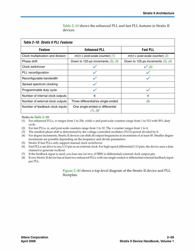
Altera Corporation 2–59April 2006 Stratix II Device Handbook, Volume 1
Stratix II Architecture
Table 2–10 shows the enhanced PLL and fast PLL features in Stratix II devices.
Figure 2–40 shows a top-level diagram of the Stratix II device and PLL floorplan.
Table 2–10. Stratix II PLL Features
Feature Enhanced PLL Fast PLL
Clock multiplication and division m/(n × post-scale counter) (1) m/(n × post-scale counter) (2)
Phase shift Down to 125-ps increments (3), (4) Down to 125-ps increments (3), (4)
Clock switchover v v (5)
PLL reconfiguration v v
Reconfigurable bandwidth v v
Spread spectrum clocking v
Programmable duty cycle v v
Number of internal clock outputs 6 4
Number of external clock outputs Three differential/six single-ended (6)
Number of feedback clock inputs One single-ended or differential(7), (8)
Notes to Table 2–10:(1) For enhanced PLLs, m ranges from 1 to 256, while n and post-scale counters range from 1 to 512 with 50% duty
cycle.(2) For fast PLLs, m, and post-scale counters range from 1 to 32. The n counter ranges from 1 to 4.(3) The smallest phase shift is determined by the voltage controlled oscillator (VCO) period divided by 8.(4) For degree increments, Stratix II devices can shift all output frequencies in increments of at least 45. Smaller degree
increments are possible depending on the frequency and divide parameters.(5) Stratix II fast PLLs only support manual clock switchover.(6) Fast PLLs can drive to any I/O pin as an external clock. For high-speed differential I/O pins, the device uses a data
channel to generate txclkout.(7) If the feedback input is used, you lose one (or two, if FBIN is differential) external clock output pin.(8) Every Stratix II device has at least two enhanced PLLs with one single-ended or differential external feedback input
per PLL.
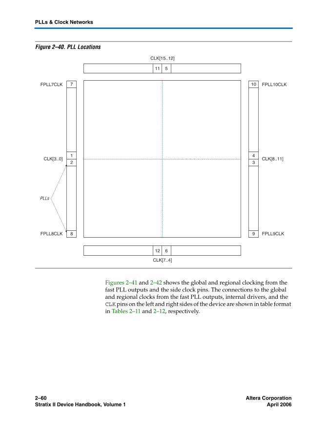
2–60 Altera CorporationStratix II Device Handbook, Volume 1 April 2006
PLLs & Clock Networks
Figure 2–40. PLL Locations
Figures 2–41 and 2–42 shows the global and regional clocking from the fast PLL outputs and the side clock pins. The connections to the global and regional clocks from the fast PLL outputs, internal drivers, and the CLK pins on the left and right sides of the device are shown in table format in Tables 2–11 and 2–12, respectively.
FPLL7CLK FPLL10CLK
FPLL9CLK
CLK[8..11]
FPLL8CLK
CLK[3..0]
7
1
2
8
10
4
3
9
511
612
CLK[7..4]
CLK[15..12]
PLLs
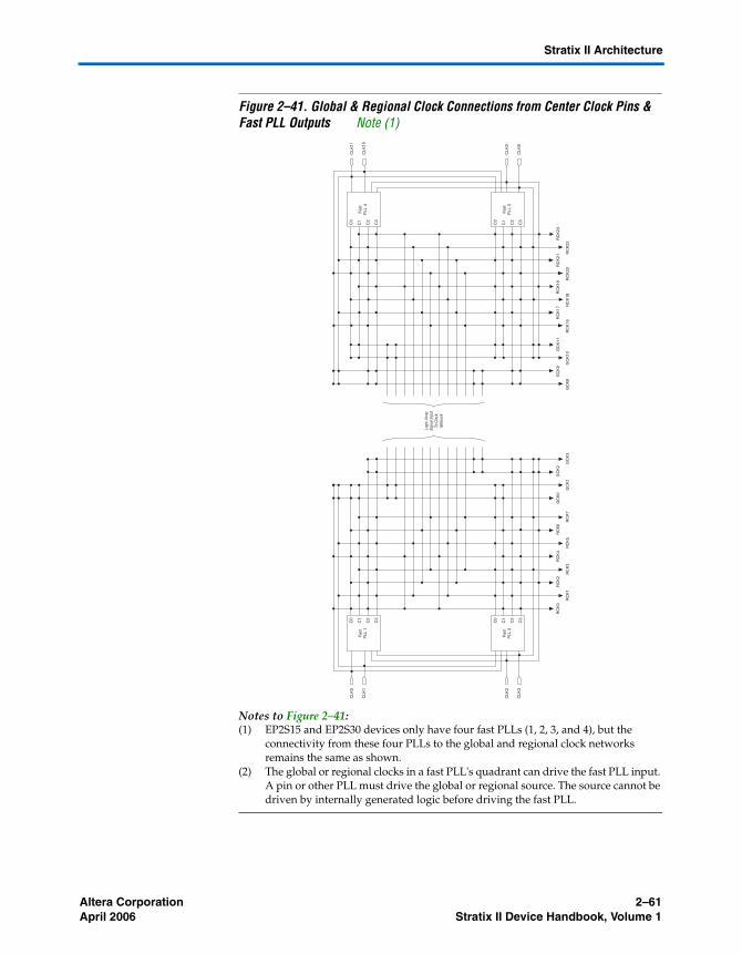
Altera Corporation 2–61April 2006 Stratix II Device Handbook, Volume 1
Stratix II Architecture
Figure 2–41. Global & Regional Clock Connections from Center Clock Pins & Fast PLL Outputs Note (1)
Notes to Figure 2–41:(1) EP2S15 and EP2S30 devices only have four fast PLLs (1, 2, 3, and 4), but the
connectivity from these four PLLs to the global and regional clock networks remains the same as shown.
(2) The global or regional clocks in a fast PLL's quadrant can drive the fast PLL input. A pin or other PLL must drive the global or regional source. The source cannot be driven by internally generated logic before driving the fast PLL.
C0
C1
C2
C3
Fast
PLL
1
RC
K0
RC
K2
RC
K1
RC
K3
GC
K0
GC
K2
GC
K9
GC
K11
GC
K1
GC
K3
GC
K8
GC
K10
RC
K4
RC
K6
RC
K5
RC
K7
RC
K17
RC
K16
RC
K18
RC
K19
RC
K21
RC
K23
RC
K20
RC
K22
C0
C1
C2
C3
Fast
PLL
2
Logi
c Ar
ray
Sign
al In
put
To C
lock
Netw
ork
CLK
0
CLK
1
CLK
2
CLK
3
C0
C1
C2
C3
Fast
PLL
4
C0
C1
C2
C3
Fast
PLL
3
CLK
11
CLK
10
CLK
9
CLK
8
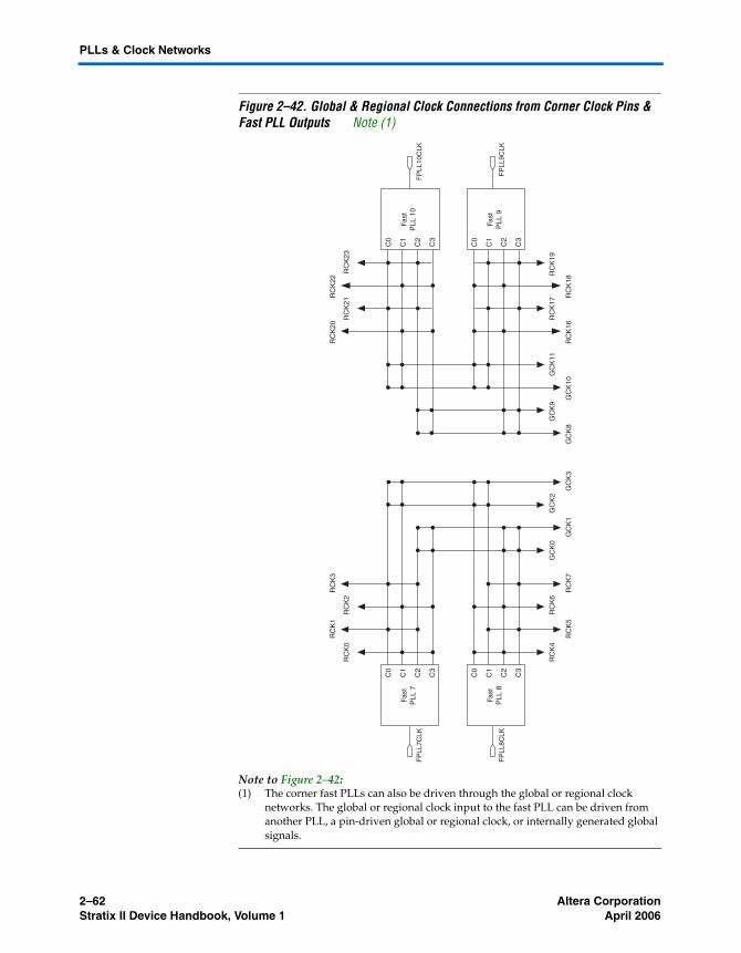
2–62 Altera CorporationStratix II Device Handbook, Volume 1 April 2006
PLLs & Clock Networks
Figure 2–42. Global & Regional Clock Connections from Corner Clock Pins & Fast PLL Outputs Note (1)
Note to Figure 2–42:(1) The corner fast PLLs can also be driven through the global or regional clock
networks. The global or regional clock input to the fast PLL can be driven from another PLL, a pin-driven global or regional clock, or internally generated global signals.
C0
C1
C2
C3
Fast
PLL
7
RC
K0
RC
K2
RC
K1
RC
K3
GC
K0
GC
K2
GC
K9
GC
K11
GC
K1
GC
K3
GC
K8
GC
K10
RC
K4
RC
K6
RC
K5
RC
K7
RC
K17
RC
K16
RC
K18
RC
K19
RC
K21
RC
K23
RC
K20
RC
K22
C0
C1
C2
C3
Fast
PLL
8
C0
C1
C2
C3
Fast
PLL
10
C0
C1
C2
C3
Fast
PLL
9
FP
LL7C
LK
FP
LL8C
LK
FP
LL10
CL K
FP
LL9C
L K
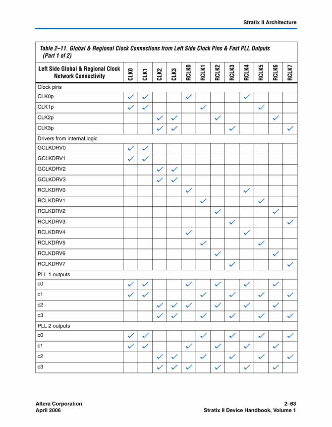
Altera Corporation 2–63April 2006 Stratix II Device Handbook, Volume 1
Stratix II Architecture
Table 2–11. Global & Regional Clock Connections from Left Side Clock Pins & Fast PLL Outputs(Part 1 of 2)
Left Side Global & Regional Clock Network Connectivity CL
K0
CLK1
CLK2
CLK3
RCLK
0
RCLK
1
RCLK
2
RCLK
3
RCLK
4
RCLK
5
RCLK
6
RCLK
7
Clock pins
CLK0p v v v v
CLK1p v v v v
CLK2p v v v v
CLK3p v v v v
Drivers from internal logic
GCLKDRV0 v v
GCLKDRV1 v v
GCLKDRV2 v v
GCLKDRV3 v v
RCLKDRV0 v v
RCLKDRV1 v v
RCLKDRV2 v v
RCLKDRV3 v v
RCLKDRV4 v v
RCLKDRV5 v v
RCLKDRV6 v v
RCLKDRV7 v v
PLL 1 outputs
c0 v v v v v v
c1 v v v v v v
c2 v v v v v v
c3 v v v v v v
PLL 2 outputs
c0 v v v v v v
c1 v v v v v v
c2 v v v v v v
c3 v v v v v v
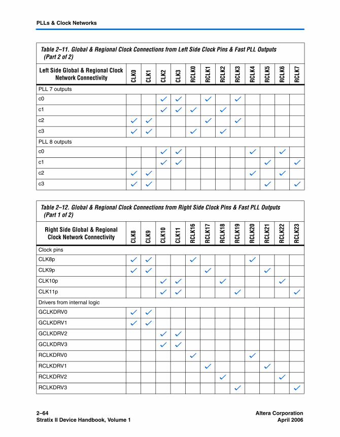
2–64 Altera CorporationStratix II Device Handbook, Volume 1 April 2006
PLLs & Clock Networks
PLL 7 outputs
c0 v v v v
c1 v v v v
c2 v v v v
c3 v v v v
PLL 8 outputs
c0 v v v v
c1 v v v v
c2 v v v v
c3 v v v v
Table 2–12. Global & Regional Clock Connections from Right Side Clock Pins & Fast PLL Outputs(Part 1 of 2)
Right Side Global & Regional Clock Network Connectivity
CLK8
CLK9
CLK1
0
CLK1
1
RCLK
16
RCLK
17
RCLK
18
RCLK
19
RCLK
20
RCLK
21
RCLK
22
RCLK
23
Clock pins
CLK8p v v v v
CLK9p v v v v
CLK10p v v v v
CLK11p v v v v
Drivers from internal logic
GCLKDRV0 v v
GCLKDRV1 v v
GCLKDRV2 v v
GCLKDRV3 v v
RCLKDRV0 v v
RCLKDRV1 v v
RCLKDRV2 v v
RCLKDRV3 v v
Table 2–11. Global & Regional Clock Connections from Left Side Clock Pins & Fast PLL Outputs(Part 2 of 2)
Left Side Global & Regional Clock Network Connectivity CL
K0
CLK1
CLK2
CLK3
RCLK
0
RCLK
1
RCLK
2
RCLK
3
RCLK
4
RCLK
5
RCLK
6
RCLK
7
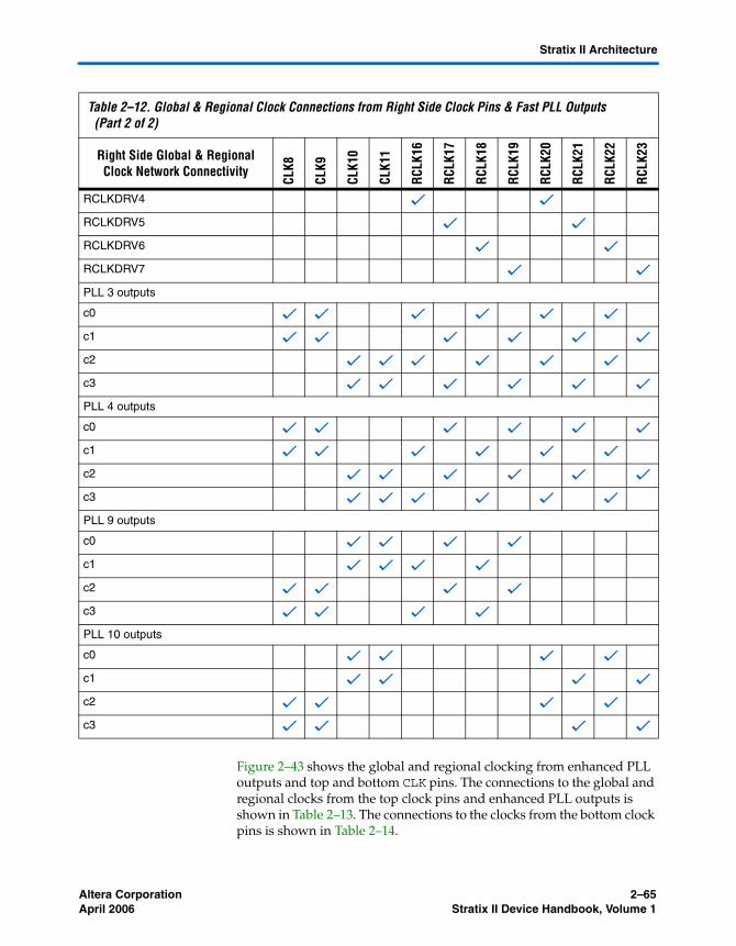
Altera Corporation 2–65April 2006 Stratix II Device Handbook, Volume 1
Stratix II Architecture
Figure 2–43 shows the global and regional clocking from enhanced PLL outputs and top and bottom CLK pins. The connections to the global and regional clocks from the top clock pins and enhanced PLL outputs is shown in Table 2–13. The connections to the clocks from the bottom clock pins is shown in Table 2–14.
RCLKDRV4 v v
RCLKDRV5 v v
RCLKDRV6 v v
RCLKDRV7 v v
PLL 3 outputs
c0 v v v v v v
c1 v v v v v v
c2 v v v v v v
c3 v v v v v v
PLL 4 outputs
c0 v v v v v v
c1 v v v v v v
c2 v v v v v v
c3 v v v v v v
PLL 9 outputs
c0 v v v v
c1 v v v v
c2 v v v v
c3 v v v v
PLL 10 outputs
c0 v v v v
c1 v v v v
c2 v v v v
c3 v v v v
Table 2–12. Global & Regional Clock Connections from Right Side Clock Pins & Fast PLL Outputs(Part 2 of 2)
Right Side Global & Regional Clock Network Connectivity
CLK8
CLK9
CLK1
0
CLK1
1
RCLK
16
RCLK
17
RCLK
18
RCLK
19
RCLK
20
RCLK
21
RCLK
22
RCLK
23
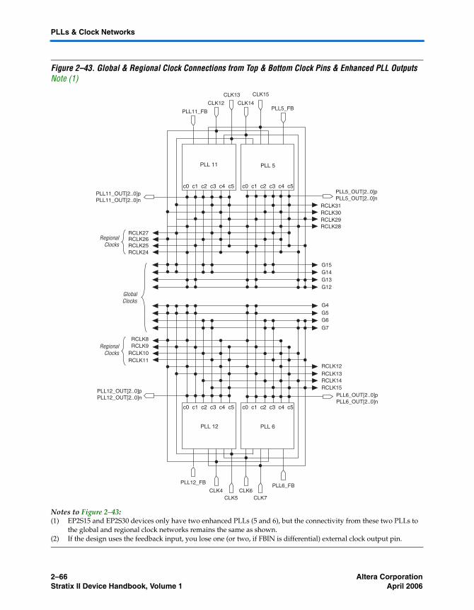
2–66 Altera CorporationStratix II Device Handbook, Volume 1 April 2006
PLLs & Clock Networks
Figure 2–43. Global & Regional Clock Connections from Top & Bottom Clock Pins & Enhanced PLL Outputs Note (1)
Notes to Figure 2–43:(1) EP2S15 and EP2S30 devices only have two enhanced PLLs (5 and 6), but the connectivity from these two PLLs to
the global and regional clock networks remains the same as shown.(2) If the design uses the feedback input, you lose one (or two, if FBIN is differential) external clock output pin.
G15G14G13G12
RCLK31RCLK30RCLK29RCLK28
RCLK27RCLK26RCLK25RCLK24
G7
G6G5G4
RCLK15RCLK14RCLK13RCLK12
RCLK11RCLK10
RCLK9RCLK8
PLL 6
CLK7CLK6
CLK5CLK4
PLL 12
PLL 5
c0 c1 c2 c3 c4 c5 c0 c1 c2 c3 c4 c5
c0 c1 c2 c3 c4 c5 c0 c1 c2 c3 c4 c5
CLK14
CLK15CLK13
CLK12
PLL 11
PLL11_FB
PLL5_OUT[2..0]pPLL5_OUT[2..0]n
PLL11_OUT[2..0]pPLL11_OUT[2..0]n
PLL12_OUT[2..0]pPLL12_OUT[2..0]n PLL6_OUT[2..0]p
PLL6_OUT[2..0]n
PLL5_FB
PLL12_FBPLL6_FB
GlobalClocks
RegionalClocks
RegionalClocks
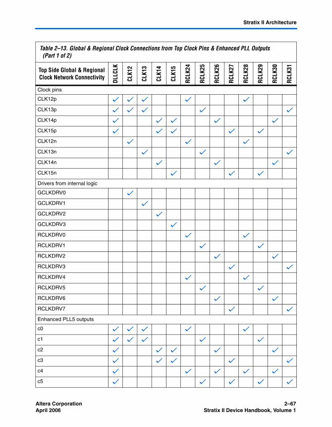
Altera Corporation 2–67April 2006 Stratix II Device Handbook, Volume 1
Stratix II Architecture
Table 2–13. Global & Regional Clock Connections from Top Clock Pins & Enhanced PLL Outputs(Part 1 of 2)
Top Side Global & Regional Clock Network Connectivity
DLLC
LK
CLK1
2
CLK1
3
CLK1
4
CLK1
5
RCLK
24
RCLK
25
RCLK
26
RCLK
27
RCLK
28
RCLK
29
RCLK
30
RCLK
31
Clock pins
CLK12p v v v v v
CLK13p v v v v v
CLK14p v v v v v
CLK15p v v v v v
CLK12n v v v
CLK13n v v v
CLK14n v v v
CLK15n v v v
Drivers from internal logic
GCLKDRV0 v
GCLKDRV1 v
GCLKDRV2 v
GCLKDRV3 v
RCLKDRV0 v v
RCLKDRV1 v v
RCLKDRV2 v v
RCLKDRV3 v v
RCLKDRV4 v v
RCLKDRV5 v v
RCLKDRV6 v v
RCLKDRV7 v v
Enhanced PLL5 outputs
c0 v v v v v
c1 v v v v v
c2 v v v v v
c3 v v v v v
c4 v v v v v
c5 v v v v v
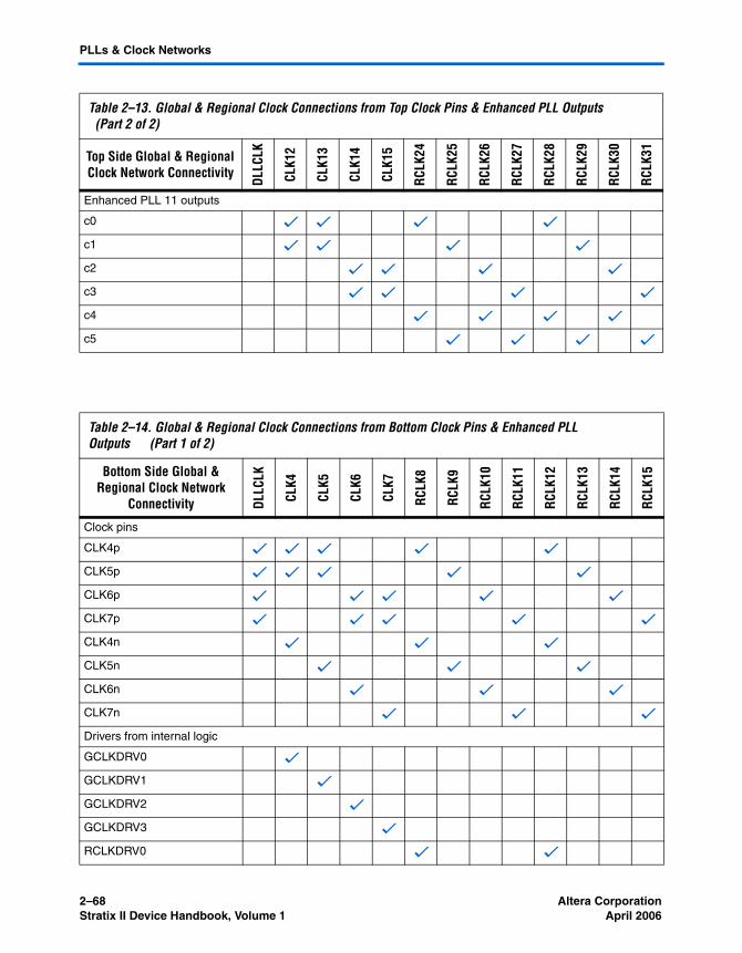
2–68 Altera CorporationStratix II Device Handbook, Volume 1 April 2006
PLLs & Clock Networks
Enhanced PLL 11 outputs
c0 v v v v
c1 v v v v
c2 v v v v
c3 v v v v
c4 v v v v
c5 v v v v
Table 2–13. Global & Regional Clock Connections from Top Clock Pins & Enhanced PLL Outputs(Part 2 of 2)
Top Side Global & Regional Clock Network Connectivity
DLLC
LK
CLK1
2
CLK1
3
CLK1
4
CLK1
5
RCLK
24
RCLK
25
RCLK
26
RCLK
27
RCLK
28
RCLK
29
RCLK
30
RCLK
31
Table 2–14. Global & Regional Clock Connections from Bottom Clock Pins & Enhanced PLL Outputs (Part 1 of 2)
Bottom Side Global & Regional Clock Network
Connectivity DLLC
LK
CLK4
CLK5
CLK6
CLK7
RCLK
8
RCLK
9
RCLK
10
RCLK
11
RCLK
12
RCLK
13
RCLK
14
RCLK
15
Clock pins
CLK4p v v v v v
CLK5p v v v v v
CLK6p v v v v v
CLK7p v v v v v
CLK4n v v v
CLK5n v v v
CLK6n v v v
CLK7n v v v
Drivers from internal logic
GCLKDRV0 v
GCLKDRV1 v
GCLKDRV2 v
GCLKDRV3 v
RCLKDRV0 v v
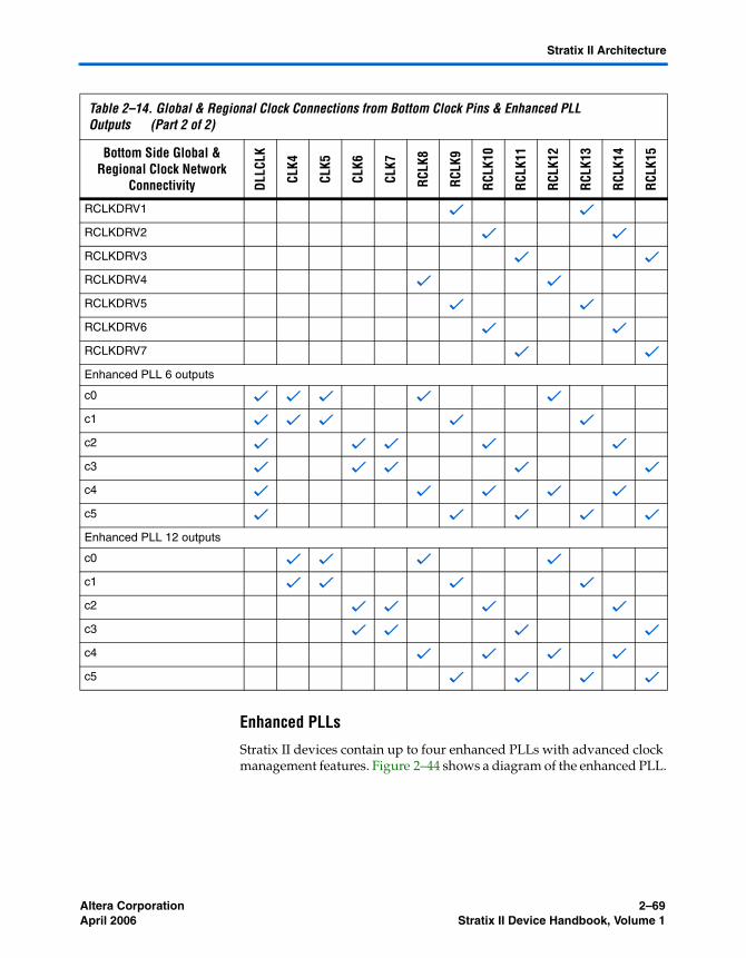
Altera Corporation 2–69April 2006 Stratix II Device Handbook, Volume 1
Stratix II Architecture
Enhanced PLLs
Stratix II devices contain up to four enhanced PLLs with advanced clock management features. Figure 2–44 shows a diagram of the enhanced PLL.
RCLKDRV1 v v
RCLKDRV2 v v
RCLKDRV3 v v
RCLKDRV4 v v
RCLKDRV5 v v
RCLKDRV6 v v
RCLKDRV7 v v
Enhanced PLL 6 outputs
c0 v v v v v
c1 v v v v v
c2 v v v v v
c3 v v v v v
c4 v v v v v
c5 v v v v v
Enhanced PLL 12 outputs
c0 v v v v
c1 v v v v
c2 v v v v
c3 v v v v
c4 v v v v
c5 v v v v
Table 2–14. Global & Regional Clock Connections from Bottom Clock Pins & Enhanced PLL Outputs (Part 2 of 2)
Bottom Side Global & Regional Clock Network
Connectivity DLLC
LK
CLK4
CLK5
CLK6
CLK7
RCLK
8
RCLK
9
RCLK
10
RCLK
11
RCLK
12
RCLK
13
RCLK
14
RCLK
15
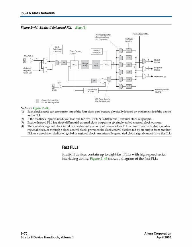
2–70 Altera CorporationStratix II Device Handbook, Volume 1 April 2006
PLLs & Clock Networks
Figure 2–44. Stratix II Enhanced PLL Note (1)
Notes to Figure 2–44:(1) Each clock source can come from any of the four clock pins that are physically located on the same side of the device
as the PLL.(2) If the feedback input is used, you lose one (or two, if FBIN is differential) external clock output pin.(3) Each enhanced PLL has three differential external clock outputs or six single-ended external clock outputs.(4) The global or regional clock input can be driven by an output from another PLL, a pin-driven dedicated global or
regional clock, or through a clock control block, provided the clock control block is fed by an output from another PLL or a pin-driven dedicated global or regional clock. An internally generated global signal cannot drive the PLL.
Fast PLLs
Stratix II devices contain up to eight fast PLLs with high-speed serial interfacing ability. Figure 2–45 shows a diagram of the fast PLL.
/n ChargePump VCO /c2
/c3
/c4
/c0
8
4
6
4 GlobalClocks
/c1
Lock Detect to I/O or generalrouting
INCLK[3..0]
FBIN
Global or RegionalClock
PFD
/c5
From Adjacent PLL
/m
SpreadSpectrum
I/O Buffers (3)
(2)
LoopFilter
& Filter
Post-ScaleCounters
ClockSwitchover
Circuitry Phase FrequencyDetector
VCO Phase SelectionSelectable at EachPLL Output Port
VCO Phase SelectionAffecting All OutputsShaded Portions of the
PLL are Reconfigurable
RegionalClocks
8
6(4)
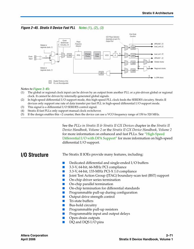
Altera Corporation 2–71April 2006 Stratix II Device Handbook, Volume 1
Stratix II Architecture
Figure 2–45. Stratix II Device Fast PLL Notes (1), (2), (3)
Notes to Figure 2–45:(1) The global or regional clock input can be driven by an output from another PLL or a pin-driven global or regional
clock. It cannot be driven by internally-generated global signals.(2) In high-speed differential I/O support mode, this high-speed PLL clock feeds the SERDES circuitry. Stratix II
devices only support one rate of data transfer per fast PLL in high-speed differential I/O support mode.(3) This signal is a differential I/O SERDES control signal.(4) Stratix II fast PLLs only support manual clock switchover.(5) If the design enables this ÷2 counter, then the device can use a VCO frequency range of 150 to 520 MHz.
See the PLLs in Stratix II & Stratix II GX Devices chapter in the Stratix II Device Handbook, Volume 2 or the Stratix II GX Device Handbook, Volume 2 for more information on enhanced and fast PLLs. See “High-Speed Differential I/O with DPA Support” for more information on high-speed differential I/O support.
I/O Structure The Stratix II IOEs provide many features, including:
■ Dedicated differential and single-ended I/O buffers■ 3.3-V, 64-bit, 66-MHz PCI compliance■ 3.3-V, 64-bit, 133-MHz PCI-X 1.0 compliance■ Joint Test Action Group (JTAG) boundary-scan test (BST) support■ On-chip driver series termination■ On-chip parallel termination■ On-chip termination for differential standards■ Programmable pull-up during configuration■ Output drive strength control■ Tri-state buffers■ Bus-hold circuitry■ Programmable pull-up resistors■ Programmable input and output delays■ Open-drain outputs■ DQ and DQS I/O pins
ChargePump VCO ÷c1
8
8
4
4
8
ClockInput
PFD
÷c0
÷m
LoopFilter
PhaseFrequencyDetector
VCO Phase SelectionSelectable at each PLLOutput Port
Post-ScaleCounters
Global clocks
diffioclk1
load_en1
load_en0
diffioclk0
Regional clocks
to DPA block
Global orregional clock (1)
Global orregional clock (1)
÷c2
÷k
÷c3
÷n4
ClockSwitchoverCircuitry (4)
Shaded Portions of thePLL are Reconfigurable
(2)
(2)
(3)
(3)
(5)
2–72 Altera CorporationStratix II Device Handbook, Volume 1 April 2006
I/O Structure
■ Double data rate (DDR) registers
The IOE in Stratix II devices contains a bidirectional I/O buffer, six registers, and a latch for a complete embedded bidirectional single data rate or DDR transfer. Figure 2–46 shows the Stratix II IOE structure. The IOE contains two input registers (plus a latch), two output registers, and two output enable registers. The design can use both input registers and the latch to capture DDR input and both output registers to drive DDR outputs. Additionally, the design can use the output enable (OE) register for fast clock-to-output enable timing. The negative edge-clocked OE register is used for DDR SDRAM interfacing. The Quartus II software automatically duplicates a single OE register that controls multiple output or bidirectional pins.
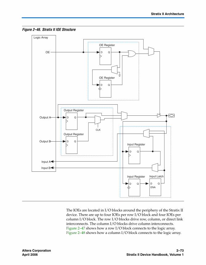
Altera Corporation 2–73April 2006 Stratix II Device Handbook, Volume 1
Stratix II Architecture
Figure 2–46. Stratix II IOE Structure
The IOEs are located in I/O blocks around the periphery of the Stratix II device. There are up to four IOEs per row I/O block and four IOEs per column I/O block. The row I/O blocks drive row, column, or direct link interconnects. The column I/O blocks drive column interconnects. Figure 2–47 shows how a row I/O block connects to the logic array. Figure 2–48 shows how a column I/O block connects to the logic array.
D Q
Output Register
Output A
D Q
Output Register
Output B
Input A
Input B
D Q
OE Register
OE
D Q
OE Register
D Q
Input Register
D Q
Input Register
D Q
Input Latch
Logic Array
CLK
ENA
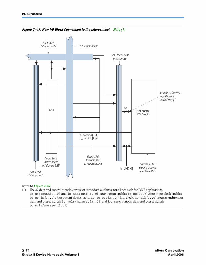
2–74 Altera CorporationStratix II Device Handbook, Volume 1 April 2006
I/O Structure
Figure 2–47. Row I/O Block Connection to the Interconnect Note (1)
Note to Figure 2–47:(1) The 32 data and control signals consist of eight data out lines: four lines each for DDR applications
io_dataouta[3..0] and io_dataoutb[3..0], four output enables io_oe[3..0], four input clock enables io_ce_in[3..0], four output clock enables io_ce_out[3..0], four clocks io_clk[3..0], four asynchronous clear and preset signals io_aclr/apreset[3..0], and four synchronous clear and preset signals io_sclr/spreset[3..0].
32
R4 & R24Interconnects C4 Interconnect
I/O Block Local Interconnect
32 Data & Control Signals from Logic Array (1)
io_dataina[3..0]io_datainb[3..0]
io_clk[7:0]
Horizontal I/OBlock Containsup to Four IOEs
Direct LinkInterconnect
to Adjacent LAB
Direct LinkInterconnect
to Adjacent LAB
LAB LocalInterconnect
LAB HorizontalI/O Block
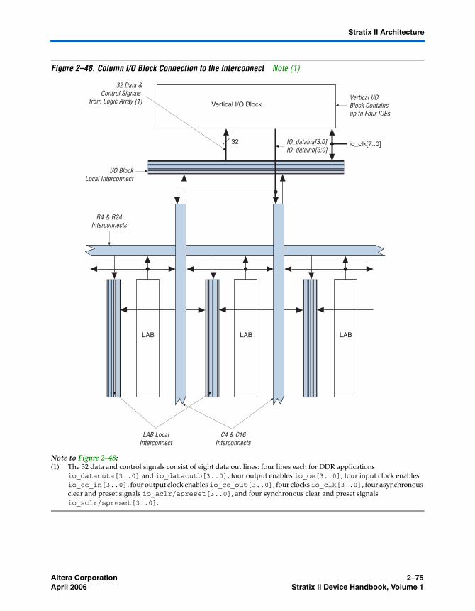
Altera Corporation 2–75April 2006 Stratix II Device Handbook, Volume 1
Stratix II Architecture
Figure 2–48. Column I/O Block Connection to the Interconnect Note (1)
Note to Figure 2–48:(1) The 32 data and control signals consist of eight data out lines: four lines each for DDR applications
io_dataouta[3..0] and io_dataoutb[3..0], four output enables io_oe[3..0], four input clock enables io_ce_in[3..0], four output clock enables io_ce_out[3..0], four clocks io_clk[3..0], four asynchronous clear and preset signals io_aclr/apreset[3..0], and four synchronous clear and preset signals io_sclr/spreset[3..0].
32 Data &Control Signals
from Logic Array (1) Vertical I/O Block Containsup to Four IOEs
I/O BlockLocal Interconnect
IO_dataina[3:0]IO_datainb[3:0]
R4 & R24Interconnects
LAB LocalInterconnect
C4 & C16Interconnects
32
LAB LAB LAB
io_clk[7..0]
Vertical I/O Block
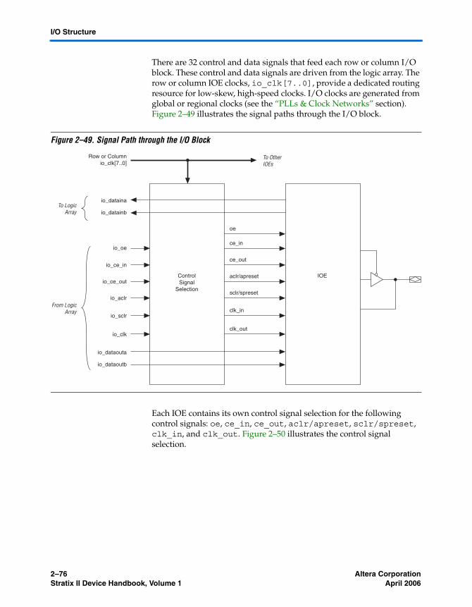
2–76 Altera CorporationStratix II Device Handbook, Volume 1 April 2006
I/O Structure
There are 32 control and data signals that feed each row or column I/O block. These control and data signals are driven from the logic array. The row or column IOE clocks, io_clk[7..0], provide a dedicated routing resource for low-skew, high-speed clocks. I/O clocks are generated from global or regional clocks (see the “PLLs & Clock Networks” section). Figure 2–49 illustrates the signal paths through the I/O block.
Figure 2–49. Signal Path through the I/O Block
Each IOE contains its own control signal selection for the following control signals: oe, ce_in, ce_out, aclr/apreset, sclr/spreset, clk_in, and clk_out. Figure 2–50 illustrates the control signal selection.
Row or Columnio_clk[7..0]
io_dataina
io_datainb
io_dataouta
io_dataoutb
io_oe
oe
ce_in
ce_outio_ce_in
aclr/apresetio_ce_out
sclr/spreset
io_sclr
io_aclr
clk_in
io_clkclk_out
ControlSignal
Selection
IOE
To LogicArray
From LogicArray
To OtherIOEs
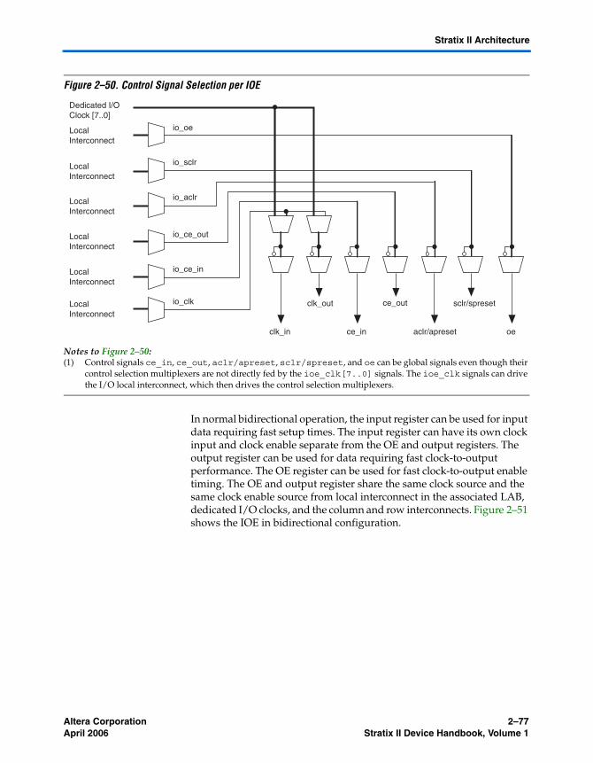
Altera Corporation 2–77April 2006 Stratix II Device Handbook, Volume 1
Stratix II Architecture
Figure 2–50. Control Signal Selection per IOE
Notes to Figure 2–50:(1) Control signals ce_in, ce_out, aclr/apreset, sclr/spreset, and oe can be global signals even though their
control selection multiplexers are not directly fed by the ioe_clk[7..0] signals. The ioe_clk signals can drive the I/O local interconnect, which then drives the control selection multiplexers.
In normal bidirectional operation, the input register can be used for input data requiring fast setup times. The input register can have its own clock input and clock enable separate from the OE and output registers. The output register can be used for data requiring fast clock-to-output performance. The OE register can be used for fast clock-to-output enable timing. The OE and output register share the same clock source and the same clock enable source from local interconnect in the associated LAB, dedicated I/O clocks, and the column and row interconnects. Figure 2–51 shows the IOE in bidirectional configuration.
clk_out
ce_inclk_in
ce_out
aclr/apreset
sclr/spreset
Dedicated I/OClock [7..0]
LocalInterconnect
LocalInterconnect
LocalInterconnect
LocalInterconnect
LocalInterconnect
oe
io_oe
io_aclr
LocalInterconnect
io_sclr
io_ce_out
io_ce_in
io_clk
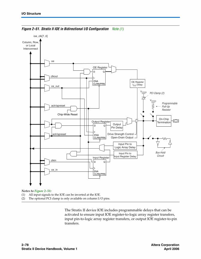
2–78 Altera CorporationStratix II Device Handbook, Volume 1 April 2006
I/O Structure
Figure 2–51. Stratix II IOE in Bidirectional I/O Configuration Note (1)
Notes to Figure 2–51:(1) All input signals to the IOE can be inverted at the IOE.(2) The optional PCI clamp is only available on column I/O pins.
The Stratix II device IOE includes programmable delays that can be activated to ensure input IOE register-to-logic array register transfers, input pin-to-logic array register transfers, or output IOE register-to-pin transfers.
CLRN/PRN
D Q
ENA
Chip-Wide Reset
OE Register
CLRN/PRN
D Q
ENA
Output Register
VCCIO
VCCIO PCI Clamp (2)
ProgrammablePull-UpResistor
Column, Row,or Local
Interconnect
ioe_clk[7..0]
Bus-HoldCircuit
OE RegistertCO Delay
CLRN/PRN
D Q
ENA
Input Register
Input Pin toInput Register Delay
Input Pin toLogic Array Delay
Drive Strength ControlOpen-Drain Output
On-ChipTermination
sclr/spreset
oe
clkout
ce_out
aclr/apreset
clkin
ce_in
OutputPin Delay
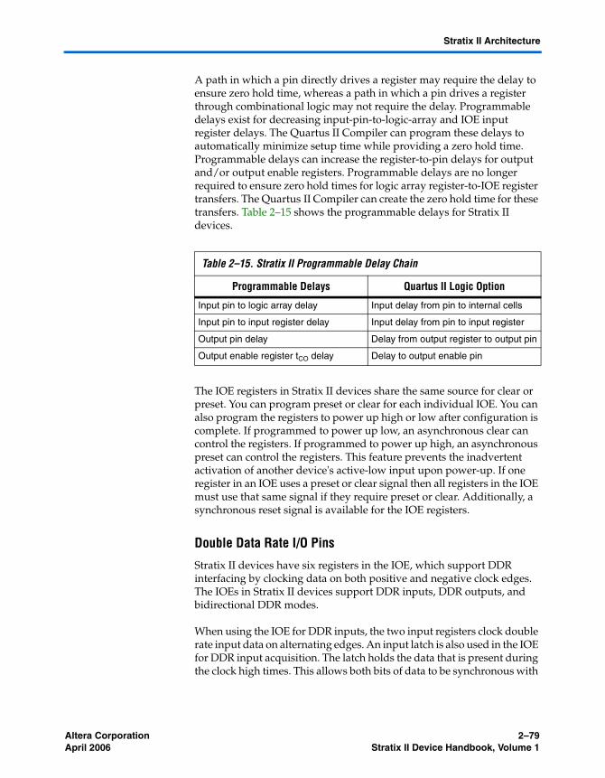
Altera Corporation 2–79April 2006 Stratix II Device Handbook, Volume 1
Stratix II Architecture
A path in which a pin directly drives a register may require the delay to ensure zero hold time, whereas a path in which a pin drives a register through combinational logic may not require the delay. Programmable delays exist for decreasing input-pin-to-logic-array and IOE input register delays. The Quartus II Compiler can program these delays to automatically minimize setup time while providing a zero hold time. Programmable delays can increase the register-to-pin delays for output and/or output enable registers. Programmable delays are no longer required to ensure zero hold times for logic array register-to-IOE register transfers. The Quartus II Compiler can create the zero hold time for these transfers. Table 2–15 shows the programmable delays for Stratix II devices.
The IOE registers in Stratix II devices share the same source for clear or preset. You can program preset or clear for each individual IOE. You can also program the registers to power up high or low after configuration is complete. If programmed to power up low, an asynchronous clear can control the registers. If programmed to power up high, an asynchronous preset can control the registers. This feature prevents the inadvertent activation of another device's active-low input upon power-up. If one register in an IOE uses a preset or clear signal then all registers in the IOE must use that same signal if they require preset or clear. Additionally, a synchronous reset signal is available for the IOE registers.
Double Data Rate I/O Pins
Stratix II devices have six registers in the IOE, which support DDR interfacing by clocking data on both positive and negative clock edges. The IOEs in Stratix II devices support DDR inputs, DDR outputs, and bidirectional DDR modes.
When using the IOE for DDR inputs, the two input registers clock double rate input data on alternating edges. An input latch is also used in the IOE for DDR input acquisition. The latch holds the data that is present during the clock high times. This allows both bits of data to be synchronous with
Table 2–15. Stratix II Programmable Delay Chain
Programmable Delays Quartus II Logic Option
Input pin to logic array delay Input delay from pin to internal cells
Input pin to input register delay Input delay from pin to input register
Output pin delay Delay from output register to output pin
Output enable register tCO delay Delay to output enable pin
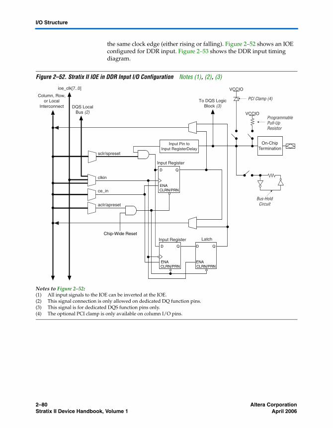
2–80 Altera CorporationStratix II Device Handbook, Volume 1 April 2006
I/O Structure
the same clock edge (either rising or falling). Figure 2–52 shows an IOE configured for DDR input. Figure 2–53 shows the DDR input timing diagram.
Figure 2–52. Stratix II IOE in DDR Input I/O Configuration Notes (1), (2), (3)
Notes to Figure 2–52:(1) All input signals to the IOE can be inverted at the IOE.(2) This signal connection is only allowed on dedicated DQ function pins.(3) This signal is for dedicated DQS function pins only.(4) The optional PCI clamp is only available on column I/O pins.
CLRN/PRN
D Q
ENA
Chip-Wide Reset
Input Register
CLRN/PRN
D Q
ENA
Input Register
VCCIO
VCCIO
PCI Clamp (4)
ProgrammablePull-UpResistor
Column, Row,or Local
Interconnect DQS LocalBus (2)
To DQS LogicBlock (3)
ioe_clk[7..0]
Bus-HoldCircuit
CLRN/PRN
D Q
ENA
Latch
Input Pin toInput RegisterDelay
sclr/spreset
clkin
aclr/apreset
On-ChipTermination
ce_in
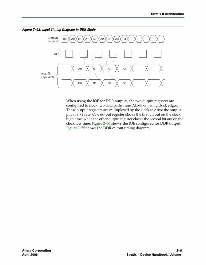
Altera Corporation 2–81April 2006 Stratix II Device Handbook, Volume 1
Stratix II Architecture
Figure 2–53. Input Timing Diagram in DDR Mode
When using the IOE for DDR outputs, the two output registers are configured to clock two data paths from ALMs on rising clock edges. These output registers are multiplexed by the clock to drive the output pin at a ×2 rate. One output register clocks the first bit out on the clock high time, while the other output register clocks the second bit out on the clock low time. Figure 2–54 shows the IOE configured for DDR output. Figure 2–55 shows the DDR output timing diagram.
Data atinput pin
CLK
A0B0 B1 A1
A1
B2 A2 A3
A2 A3
B1
A0
B0 B2 B3
B3 B4
Input ToLogic Array
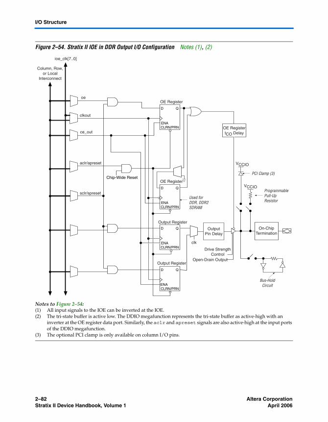
2–82 Altera CorporationStratix II Device Handbook, Volume 1 April 2006
I/O Structure
Figure 2–54. Stratix II IOE in DDR Output I/O Configuration Notes (1), (2)
Notes to Figure 2–54:(1) All input signals to the IOE can be inverted at the IOE.(2) The tri-state buffer is active low. The DDIO megafunction represents the tri-state buffer as active-high with an
inverter at the OE register data port. Similarly, the aclr and apreset signals are also active-high at the input ports of the DDIO megafunction.
(3) The optional PCI clamp is only available on column I/O pins.
CLRN/PRN
D Q
ENA
Chip-Wide Reset
OE Register
CLRN/PRN
D Q
ENA
OE Register
CLRN/PRN
D Q
ENA
Output Register
VCCIO
VCCIO
PCI Clamp (3)
ProgrammablePull-UpResistor
Column, Row,or Local
Interconnect
ioe_clk[7..0]
Bus-HoldCircuit
OE RegistertCO Delay
CLRN/PRN
D Q
ENA
Output Register
Drive StrengthControl
Open-Drain Output
Used forDDR, DDR2SDRAM
sclr/spreset
aclr/apreset
clkout
OutputPin Delay
On-ChipTermination
oe
ce_out
clk
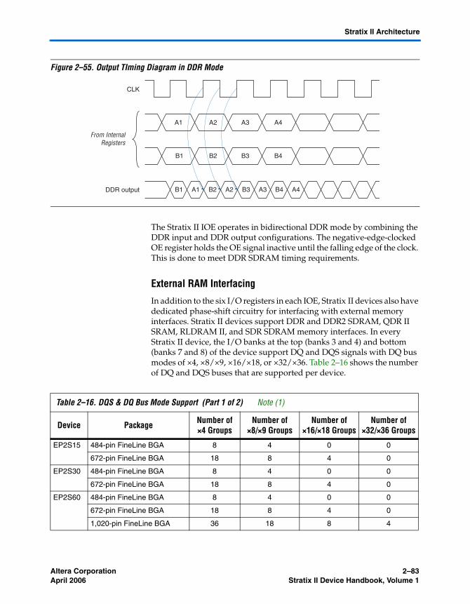
Altera Corporation 2–83April 2006 Stratix II Device Handbook, Volume 1
Stratix II Architecture
Figure 2–55. Output TIming Diagram in DDR Mode
The Stratix II IOE operates in bidirectional DDR mode by combining the DDR input and DDR output configurations. The negative-edge-clocked OE register holds the OE signal inactive until the falling edge of the clock. This is done to meet DDR SDRAM timing requirements.
External RAM Interfacing
In addition to the six I/O registers in each IOE, Stratix II devices also have dedicated phase-shift circuitry for interfacing with external memory interfaces. Stratix II devices support DDR and DDR2 SDRAM, QDR II SRAM, RLDRAM II, and SDR SDRAM memory interfaces. In every Stratix II device, the I/O banks at the top (banks 3 and 4) and bottom (banks 7 and 8) of the device support DQ and DQS signals with DQ bus modes of ×4, ×8/×9, ×16/×18, or ×32/×36. Table 2–16 shows the number of DQ and DQS buses that are supported per device.
From InternalRegisters
DDR output
CLK
B1 A1 B2 A2 B3 A3 B4 A4
A2A1 A3 A4
B1 B2 B3 B4
Table 2–16. DQS & DQ Bus Mode Support (Part 1 of 2) Note (1)
Device Package Number of ×4 Groups
Number of ×8/×9 Groups
Number of ×16/×18 Groups
Number of ×32/×36 Groups
EP2S15 484-pin FineLine BGA 8 4 0 0
672-pin FineLine BGA 18 8 4 0
EP2S30 484-pin FineLine BGA 8 4 0 0
672-pin FineLine BGA 18 8 4 0
EP2S60 484-pin FineLine BGA 8 4 0 0
672-pin FineLine BGA 18 8 4 0
1,020-pin FineLine BGA 36 18 8 4
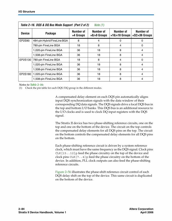
2–84 Altera CorporationStratix II Device Handbook, Volume 1 April 2006
I/O Structure
A compensated delay element on each DQS pin automatically aligns input DQS synchronization signals with the data window of their corresponding DQ data signals. The DQS signals drive a local DQS bus in the top and bottom I/O banks. This DQS bus is an additional resource to the I/O clocks and is used to clock DQ input registers with the DQS signal.
The Stratix II device has two phase-shifting reference circuits, one on the top and one on the bottom of the device. The circuit on the top controls the compensated delay elements for all DQS pins on the top. The circuit on the bottom controls the compensated delay elements for all DQS pins on the bottom.
Each phase-shifting reference circuit is driven by a system reference clock, which must have the same frequency as the DQS signal. Clock pins CLK[15..12]p feed the phase circuitry on the top of the device and clock pins CLK[7..4]p feed the phase circuitry on the bottom of the device. In addition, PLL clock outputs can also feed the phase-shifting reference circuits.
Figure 2–56 illustrates the phase-shift reference circuit control of each DQS delay shift on the top of the device. This same circuit is duplicated on the bottom of the device.
EP2S90 484-pin Hybrid FineLine BGA 8 4 0 0
780-pin FineLine BGA 18 8 4 0
1,020-pin FineLine BGA 36 18 8 4
1,508-pin FineLine BGA 36 18 8 4
EP2S130 780-pin FineLine BGA 18 8 4 0
1,020-pin FineLine BGA 36 18 8 4
1,508-pin FineLine BGA 36 18 8 4
EP2S180 1,020-pin FineLine BGA 36 18 8 4
1,508-pin FineLine BGA 36 18 8 4
Notes to Table 2–16:(1) Check the pin table for each DQS/DQ group in the different modes.
Table 2–16. DQS & DQ Bus Mode Support (Part 2 of 2) Note (1)
Device Package Number of ×4 Groups
Number of ×8/×9 Groups
Number of ×16/×18 Groups
Number of ×32/×36 Groups
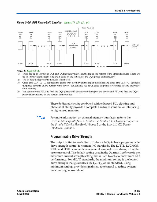
Altera Corporation 2–85April 2006 Stratix II Device Handbook, Volume 1
Stratix II Architecture
Figure 2–56. DQS Phase-Shift Circuitry Notes (1), (2), (3), (4)
Notes to Figure 2–56:(1) There are up to 18 pairs of DQS and DQSn pins available on the top or the bottom of the Stratix II device. There are
up to 10 pairs on the right side and 8 pairs on the left side of the DQS phase-shift circuitry.(2) The Δt module represents the DQS logic block.(3) Clock pins CLK[15..12]p feed the phase-shift circuitry on the top of the device and clock pins CLK[7..4]p feed
the phase circuitry on the bottom of the device. You can also use a PLL clock output as a reference clock to the phase-shift circuitry.
(4) You can only use PLL 5 to feed the DQS phase-shift circuitry on the top of the device and PLL 6 to feed the DQS phase-shift circuitry on the bottom of the device.
These dedicated circuits combined with enhanced PLL clocking and phase-shift ability provide a complete hardware solution for interfacing to high-speed memory.
f For more information on external memory interfaces, refer to the External Memory Interfaces in Stratix II & Stratix II GX Devices chapter in the Stratix II Device Handbook, Volume 2 or the Stratix II GX Device Handbook, Volume 2.
Programmable Drive Strength
The output buffer for each Stratix II device I/O pin has a programmable drive strength control for certain I/O standards. The LVTTL, LVCMOS, SSTL, and HSTL standards have several levels of drive strength that the user can control. The default setting used in the Quartus II software is the maximum current strength setting that is used to achieve maximum I/O performance. For all I/O standards, the minimum setting is the lowest drive strength that guarantees the IOH/IOL of the standard. Using minimum settings provides signal slew rate control to reduce system noise and signal overshoot.
DQSPin
DQSnPin
DQSnPin
DQSPin
DQSPin
DQSnPin
DQSPin
DQSnPin
From PLL 5 (3)
CLK[15..12]p (2)
to IOE to IOE to IOE to IOEto IOE to IOEto IOE
ΔtΔtΔtΔtΔtΔt Δt
to IOE
DQSPhase-Shift
CircuitryΔt DQS Logic
Blocks
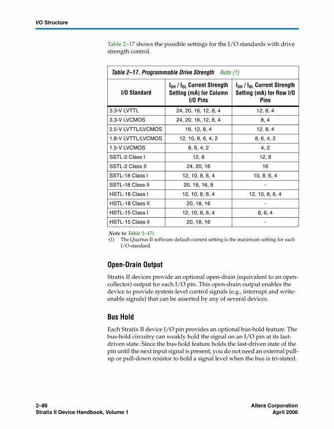
2–86 Altera CorporationStratix II Device Handbook, Volume 1 April 2006
I/O Structure
Table 2–17 shows the possible settings for the I/O standards with drive strength control.
Open-Drain Output
Stratix II devices provide an optional open-drain (equivalent to an open-collector) output for each I/O pin. This open-drain output enables the device to provide system-level control signals (e.g., interrupt and write-enable signals) that can be asserted by any of several devices.
Bus Hold
Each Stratix II device I/O pin provides an optional bus-hold feature. The bus-hold circuitry can weakly hold the signal on an I/O pin at its last-driven state. Since the bus-hold feature holds the last-driven state of the pin until the next input signal is present, you do not need an external pull-up or pull-down resistor to hold a signal level when the bus is tri-stated.
Table 2–17. Programmable Drive Strength Note (1)
I/O StandardIOH / IOL Current Strength Setting (mA) for Column
I/O Pins
IOH / IOL Current Strength Setting (mA) for Row I/O
Pins
3.3-V LVTTL 24, 20, 16, 12, 8, 4 12, 8, 4
3.3-V LVCMOS 24, 20, 16, 12, 8, 4 8, 4
2.5-V LVTTL/LVCMOS 16, 12, 8, 4 12, 8, 4
1.8-V LVTTL/LVCMOS 12, 10, 8, 6, 4, 2 8, 6, 4, 2
1.5-V LVCMOS 8, 6, 4, 2 4, 2
SSTL-2 Class I 12, 8 12, 8
SSTL-2 Class II 24, 20, 16 16
SSTL-18 Class I 12, 10, 8, 6, 4 10, 8, 6, 4
SSTL-18 Class II 20, 18, 16, 8 -
HSTL-18 Class I 12, 10, 8, 6, 4 12, 10, 8, 6, 4
HSTL-18 Class II 20, 18, 16 -
HSTL-15 Class I 12, 10, 8, 6, 4 8, 6, 4
HSTL-15 Class II 20, 18, 16 -
Note to Table 2–17:(1) The Quartus II software default current setting is the maximum setting for each
I/O standard.
Altera Corporation 2–87April 2006 Stratix II Device Handbook, Volume 1
Stratix II Architecture
The bus-hold circuitry also pulls undriven pins away from the input threshold voltage where noise can cause unintended high-frequency switching. You can select this feature individually for each I/O pin. The bus-hold output drives no higher than VCCIO to prevent overdriving signals. If the bus-hold feature is enabled, the programmable pull-up option cannot be used. Disable the bus-hold feature when the I/O pin has been configured for differential signals.
The bus-hold circuitry uses a resistor with a nominal resistance (RBH) of approximately 7 kΩ to weakly pull the signal level to the last-driven state. See the DC & Switching Characteristics chapter in the Stratix II Device Handbook, Volume 1, for the specific sustaining current driven through this resistor and overdrive current used to identify the next-driven input level. This information is provided for each VCCIO voltage level.
The bus-hold circuitry is active only after configuration. When going into user mode, the bus-hold circuit captures the value on the pin present at the end of configuration.
Programmable Pull-Up Resistor
Each Stratix II device I/O pin provides an optional programmable pull-up resistor during user mode. If you enable this feature for an I/O pin, the pull-up resistor (typically 25 kΩ) weakly holds the output to the VCCIO level of the output pin’s bank.
Programmable pull-up resistors are only supported on user I/O pins, and are not supported on dedicated configuration pins, JTAG pins or dedicated clock pins.
Advanced I/O Standard Support
Stratix II device IOEs support the following I/O standards:
■ 3.3-V LVTTL/LVCMOS■ 2.5-V LVTTL/LVCMOS■ 1.8-V LVTTL/LVCMOS■ 1.5-V LVCMOS■ 3.3-V PCI■ 3.3-V PCI-X mode 1■ LVDS■ LVPECL (on input and output clocks only)■ HyperTransport technology■ Differential 1.5-V HSTL Class I and II■ Differential 1.8-V HSTL Class I and II■ Differential SSTL-18 Class I and II■ Differential SSTL-2 Class I and II
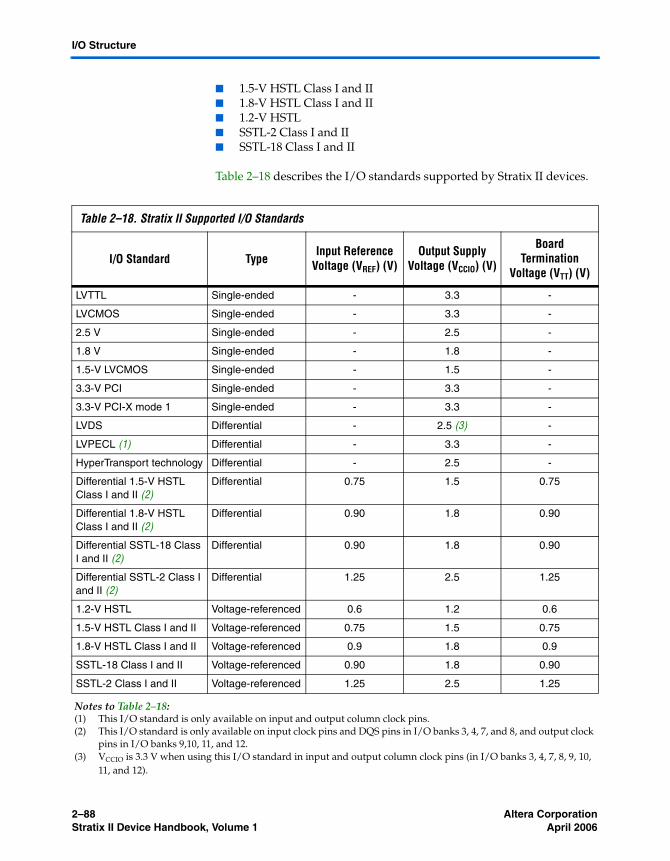
2–88 Altera CorporationStratix II Device Handbook, Volume 1 April 2006
I/O Structure
■ 1.5-V HSTL Class I and II■ 1.8-V HSTL Class I and II■ 1.2-V HSTL■ SSTL-2 Class I and II■ SSTL-18 Class I and II
Table 2–18 describes the I/O standards supported by Stratix II devices.
Table 2–18. Stratix II Supported I/O Standards
I/O Standard TypeInput Reference
Voltage (VREF) (V)Output Supply
Voltage (VCCIO) (V)
Board Termination
Voltage (VTT) (V)
LVTTL Single-ended - 3.3 -
LVCMOS Single-ended - 3.3 -
2.5 V Single-ended - 2.5 -
1.8 V Single-ended - 1.8 -
1.5-V LVCMOS Single-ended - 1.5 -
3.3-V PCI Single-ended - 3.3 -
3.3-V PCI-X mode 1 Single-ended - 3.3 -
LVDS Differential - 2.5 (3) -
LVPECL (1) Differential - 3.3 -
HyperTransport technology Differential - 2.5 -
Differential 1.5-V HSTL Class I and II (2)
Differential 0.75 1.5 0.75
Differential 1.8-V HSTL Class I and II (2)
Differential 0.90 1.8 0.90
Differential SSTL-18 Class I and II (2)
Differential 0.90 1.8 0.90
Differential SSTL-2 Class I and II (2)
Differential 1.25 2.5 1.25
1.2-V HSTL Voltage-referenced 0.6 1.2 0.6
1.5-V HSTL Class I and II Voltage-referenced 0.75 1.5 0.75
1.8-V HSTL Class I and II Voltage-referenced 0.9 1.8 0.9
SSTL-18 Class I and II Voltage-referenced 0.90 1.8 0.90
SSTL-2 Class I and II Voltage-referenced 1.25 2.5 1.25
Notes to Table 2–18:(1) This I/O standard is only available on input and output column clock pins.(2) This I/O standard is only available on input clock pins and DQS pins in I/O banks 3, 4, 7, and 8, and output clock
pins in I/O banks 9,10, 11, and 12.(3) VCCIO is 3.3 V when using this I/O standard in input and output column clock pins (in I/O banks 3, 4, 7, 8, 9, 10,
11, and 12).
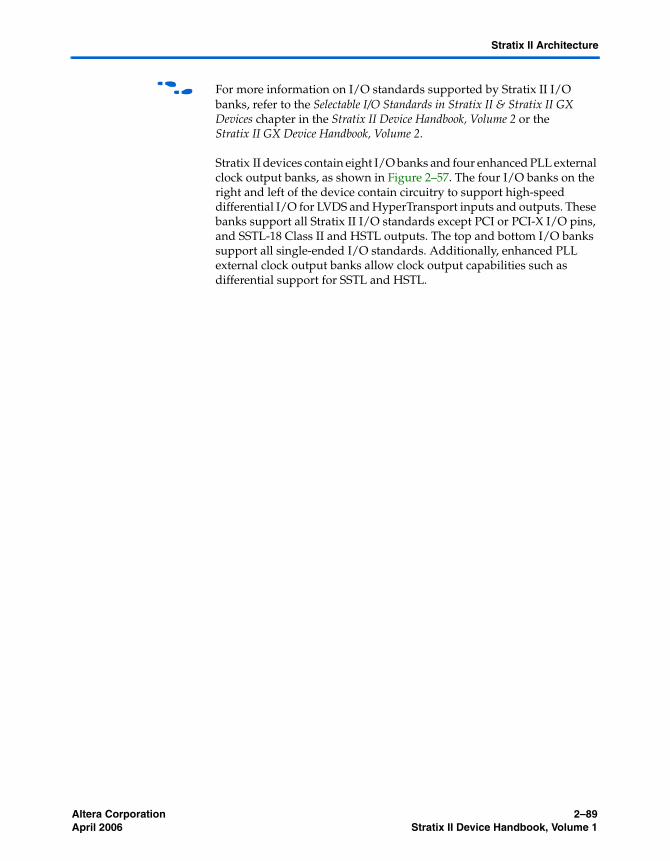
Altera Corporation 2–89April 2006 Stratix II Device Handbook, Volume 1
Stratix II Architecture
f For more information on I/O standards supported by Stratix II I/O banks, refer to the Selectable I/O Standards in Stratix II & Stratix II GX Devices chapter in the Stratix II Device Handbook, Volume 2 or the Stratix II GX Device Handbook, Volume 2.
Stratix II devices contain eight I/O banks and four enhanced PLL external clock output banks, as shown in Figure 2–57. The four I/O banks on the right and left of the device contain circuitry to support high-speed differential I/O for LVDS and HyperTransport inputs and outputs. These banks support all Stratix II I/O standards except PCI or PCI-X I/O pins, and SSTL-18 Class II and HSTL outputs. The top and bottom I/O banks support all single-ended I/O standards. Additionally, enhanced PLL external clock output banks allow clock output capabilities such as differential support for SSTL and HSTL.
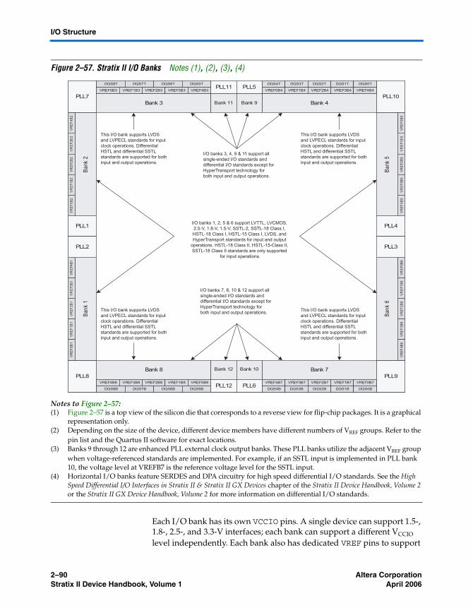
2–90 Altera CorporationStratix II Device Handbook, Volume 1 April 2006
I/O Structure
Figure 2–57. Stratix II I/O Banks Notes (1), (2), (3), (4)
Notes to Figure 2–57:(1) Figure 2–57 is a top view of the silicon die that corresponds to a reverse view for flip-chip packages. It is a graphical
representation only. (2) Depending on the size of the device, different device members have different numbers of VREF groups. Refer to the
pin list and the Quartus II software for exact locations.(3) Banks 9 through 12 are enhanced PLL external clock output banks. These PLL banks utilize the adjacent VREF group
when voltage-referenced standards are implemented. For example, if an SSTL input is implemented in PLL bank 10, the voltage level at VREFB7 is the reference voltage level for the SSTL input.
(4) Horizontal I/O banks feature SERDES and DPA circuitry for high speed differential I/O standards. See the High Speed Differential I/O Interfaces in Stratix II & Stratix II GX Devices chapter of the Stratix II Device Handbook, Volume 2 or the Stratix II GX Device Handbook, Volume 2 for more information on differential I/O standards.
Each I/O bank has its own VCCIO pins. A single device can support 1.5-, 1.8-, 2.5-, and 3.3-V interfaces; each bank can support a different VCCIO
level independently. Each bank also has dedicated VREF pins to support
Bank 3 Bank 4Bank 11 Bank 9
PLL11 PLL5
PLL7
PLL1
PLL2
PLL4
PLL3
PLL10
I/O banks 7, 8, 10 & 12 support all
single-ended I/O standards and
differential I/O standards except for
HyperTransport technology for
both input and output operations.
I/O banks 3, 4, 9 & 11 support all
single-ended I/O standards and
differential I/O standards except for
HyperTransport technology for
both input and output operations.
VREF0B3 VREF1B3 VREF2B3 VREF3B3 VREF4B3 VREF0B4 VREF1B4 VREF2B4 VREF3B4 VREF4B4
Bank 8 Bank 7Bank 12 Bank 10
PLL12 PLL6
PLL8 PLL9VREF4B8 VREF3B8 VREF2B8 VREF1B8 VREF0B8 VREF4B7 VREF3B7 VREF2B7 VREF1B7 VREF0B7
VR
EF
3B
2V
RE
F2
B2
VR
EF
1B
2V
RE
F0
B2
Ba
nk 2
VR
EF
3B
1V
RE
F2
B1
VR
EF
1B
1V
RE
F0
B1
Ban
k 1
VR
EF
1B
5V
RE
F2
B5
VR
EF
3B
5V
RE
F4
B5
Ba
nk 5
VR
EF
1B
6V
RE
F2
B6
VR
EF
3B
6V
RE
F4
B6
Ban
k 6
VR
EF
4B
2
VR
EF
0B
5
VR
EF
4B
1
VR
EF
0B
6
DQS4T DQS3T DQS2T DQS1T DQS0T
DQS4B DQS3B DQS2B DQS1B DQS0BDQS8B DQS7B DQS6B DQS5B
DQS8T DQS7T DQS6T DQS5T
This I/O bank supports LVDS
and LVPECL standards for input
clock operations. Differential
HSTL and differential SSTL
standards are supported for both
input and output operations.
This I/O bank supports LVDS
and LVPECL standards for input
clock operations. Differential
HSTL and differential SSTL
standards are supported for both
input and output operations.
This I/O bank supports LVDS
and LVPECL standards for input
clock operations. Differential
HSTL and differential SSTL
standards are supported for both
input and output operations.
This I/O bank supports LVDS
and LVPECL standards for input
clock operations. Differential
HSTL and differential SSTL
standards are supported for both
input and output operations.
I/O banks 1, 2, 5 & 6 support LVTTL, LVCMOS,
2.5-V, 1.8-V, 1.5-V, SSTL-2, SSTL-18 Class I,
HSTL-18 Class I, HSTL-15 Class I, LVDS, and
HyperTransport standards for input and output
operations. HSTL-18 Class II, HSTL-15-Class II,
SSTL-18 Class II standards are only supported
for input operations.
Altera Corporation 2–91April 2006 Stratix II Device Handbook, Volume 1
Stratix II Architecture
the voltage-referenced standards (such as SSTL-2). The PLL banks utilize the adjacent VREF group when voltage-referenced standards are implemented. For example, if an SSTL input is implemented in PLL bank 10, the voltage level at VREFB7 is the reference voltage level for the SSTL input.
I/O pins that reside in PLL banks 9 through 12 are powered by the VCC_PLL<5, 6, 11, or 12>_OUT pins, respectively. The EP2S60F484, EP2S60F780, EP2S90H484, EP2S90F780, and EP2S130F780 devices do not support PLLs 11 and 12. Therefore, any I/O pins that reside in bank 11 are powered by the VCCIO3 pin, and any I/O pins that reside in bank 12 are powered by the VCCIO8 pin.
Each I/O bank can support multiple standards with the same VCCIO for input and output pins. Each bank can support one VREF voltage level. For example, when VCCIO is 3.3 V, a bank can support LVTTL, LVCMOS, and 3.3-V PCI for inputs and outputs.
On-Chip Termination
Stratix II devices provide differential (for the LVDS or HyperTransport technology I/O standard), series, and parallel on-chip termination to reduce reflections and maintain signal integrity. On-chip termination simplifies board design by minimizing the number of external termination resistors required. Termination can be placed inside the package, eliminating small stubs that can still lead to reflections.
Stratix II devices provide four types of termination:
■ Differential termination (RD)■ Series termination (RS) without calibration■ Series termination (RS) with calibration■ Parallel termination (RT) with calibration
2–92 Altera CorporationStratix II Device Handbook, Volume 1 April 2006
I/O Structure
Table 2–19 shows the Stratix II on-chip termination support per I/O bank.
Table 2–19. On-Chip Termination Support by I/O Banks (Part 1 of 2)
On-Chip Termination Support I/O Standard Support Top & Bottom Banks Left & Right Banks
Series termination without calibration
3.3-V LVTTL v v
3.3-V LVCMOS v v
2.5-V LVTTL v v
2.5-V LVCMOS v v
1.8-V LVTTL v v
1.8-V LVCMOS v v
1.5-V LVTTL v v
1.5-V LVCMOS v v
SSTL-2 Class I and II v v
SSTL-18 Class I v v
SSTL-18 Class II v
1.8-V HSTL Class I v v
1.8-V HSTL Class II v
1.5-V HSTL Class I v v
1.2-V HSTL v
Altera Corporation 2–93April 2006 Stratix II Device Handbook, Volume 1
Stratix II Architecture
Differential On-Chip Termination
Stratix II devices support internal differential termination with a nominal resistance value of 100 Ω for LVDS or HyperTransport technology input receiver buffers. LVPECL input signals (supported on clock pins only) require an external termination resistor. Differential on-chip termination
Series termination with calibration
3.3-V LVTTL v
3.3-V LVCMOS v
2.5-V LVTTL v
2.5-V LVCMOS v
1.8-V LVTTL v
1.8-V LVCMOS v
1.5-V LVTTL v
1.5-V LVCMOS v
SSTL-2 Class I and II v
SSTL-18 Class I and II v
1.8-V HSTL Class I v
1.8-V HSTL Class II v
1.5-V HSTL Class I v
1.2-V HSTL v
Parallel termination with calibration
SSTL-2 Class I and II v
SSTL-18 Class I and II v
1.8-V HSTL Class I v
1.8-V HSTL Class II v
1.5-V HSTL Class I and II v
1.2-V HSTL v
Differential termination (1) LVDS v
HyperTransport technology v
Note to Table 2–19:(1) Clock pins CLK1, CLK3, CLK9, CLK11, and pins FPLL[7..10]CLK do not support differential on-chip
termination. Clock pins CLK0, CLK2, CLK8, and CLK10 do support differential on-chip termination. Clock pins in the top and bottom banks (CLK[4..7, 12..15]) do not support differential on-chip termination.
Table 2–19. On-Chip Termination Support by I/O Banks (Part 2 of 2)
On-Chip Termination Support I/O Standard Support Top & Bottom Banks Left & Right Banks
2–94 Altera CorporationStratix II Device Handbook, Volume 1 April 2006
I/O Structure
is supported across the full range of supported differential data rates as shown in the DC & Switching Characteristics chapter of the Stratix II Device Handbook, Volume 1.
f For more information on differential on-chip termination, refer to the High-Speed Differential I/O Interfaces with DPA in Stratix II & Stratix II GX Devices chapter of the Stratix II Device Handbook, Volume 2 or the Stratix II GX Device Handbook, Volume 2.
For more information on tolerance specifications for differential on-chip termination, refer to the DC & Switching Characteristics chapter of the Stratix II Device Handbook, Volume 1.
On-Chip Series Termination Without Calibration
Stratix II devices support driver impedance matching to provide the I/O driver with controlled output impedance that closely matches the impedance of the transmission line. As a result, reflections can be significantly reduced. Stratix II devices support on-chip series termination for single-ended I/O standards with typical RS values of 25 and 50 Ω. Once matching impedance is selected, current drive strength is no longer selectable. Table 2–19 shows the list of output standards that support on-chip series termination without calibration.
On-Chip Series Termination with Calibration
Stratix II devices support on-chip series termination with calibration in column I/O pins in top and bottom banks. There is one calibration circuit for the top I/O banks and one circuit for the bottom I/O banks. Each on-chip series termination calibration circuit compares the total impedance of each I/O buffer to the external 25- or 50-Ω resistors connected to the RUP and RDN pins, and dynamically enables or disables the transistors until they match. Calibration occurs at the end of device configuration. Once the calibration circuit finds the correct impedance, it powers down and stops changing the characteristics of the drivers.
f For more information on series on-chip termination supported by Stratix II devices, refer to the Selectable I/O Standards in Stratix II & Stratix II GX Devices chapter of the Stratix II Device Handbook, Volume 2 or the Stratix II GX Device Handbook, Volume 2.
For more information on tolerance specifications for on-chip termination with calibration, refer to the DC & Switching Characteristics chapter of the Stratix II Device Handbook, Volume 1.
Altera Corporation 2–95April 2006 Stratix II Device Handbook, Volume 1
Stratix II Architecture
On-Chip Parallel Termination with Calibration
Stratix II devices support on-chip parallel termination with calibration for column I/O pins only. There is one calibration circuit for the top I/O banks and one circuit for the bottom I/O banks. Each on-chip parallel termination calibration circuit compares the total impedance of each I/O buffer to the external 50-Ω resistors connected to the RUP and RDN pins and dynamically enables or disables the transistors until they match. Calibration occurs at the end of device configuration. Once the calibration circuit finds the correct impedance, it powers down and stops changing the characteristics of the drivers.
1 On-chip parallel termination with calibration is only supported for input pins.
f For more information on on-chip termination supported by Stratix II devices, refer to the Selectable I/O Standards in Stratix II & Stratix II GX Devices chapter of the Stratix II Device Handbook, Volume 2 or the Stratix II GX Device Handbook, Volume 2.
For more information on tolerance specifications for on-chip termination with calibration, refer to the DC & Switching Characteristics chapter of the Stratix II Device Handbook, Volume 1.
MultiVolt I/O Interface
The Stratix II architecture supports the MultiVolt I/O interface feature that allows Stratix II devices in all packages to interface with systems of different supply voltages.
The Stratix II VCCINT pins must always be connected to a 1.2-V power supply. With a 1.2-V VCCINT level, input pins are 1.5-, 1.8-, 2.5-, and 3.3-V tolerant. The VCCIO pins can be connected to either a 1.5-, 1.8-, 2.5-, or 3.3-V power supply, depending on the output requirements. The output levels are compatible with systems of the same voltage as the power supply (for example, when VCCIO pins are connected to a 1.5-V power supply, the output levels are compatible with 1.5-V systems).
The Stratix II VCCPD power pins must be connected to a 3.3-V power supply. These power pins are used to supply the pre-driver power to the output buffers, which increases the performance of the output pins. The VCCPD pins also power configuration input pins and JTAG input pins.
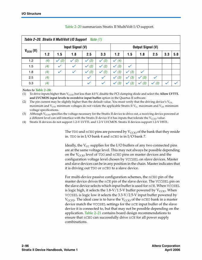
2–96 Altera CorporationStratix II Device Handbook, Volume 1 April 2006
I/O Structure
Table 2–20 summarizes Stratix II MultiVolt I/O support.
The TDO and nCEO pins are powered by VCCIO of the bank that they reside in. TDO is in I/O bank 4 and nCEO is in I/O bank 7.
Ideally, the VCC supplies for the I/O buffers of any two connected pins are at the same voltage level. This may not always be possible depending on the VCCIO level of TDO and nCEO pins on master devices and the configuration voltage level chosen by VCCSEL on slave devices. Master and slave devices can be in any position in the chain. Master indicates that it is driving out TDO or nCEO to a slave device.
For multi-device passive configuration schemes, the nCEO pin of the master device drives the nCE pin of the slave device. The VCCSEL pin on the slave device selects which input buffer is used for nCE. When VCCSEL is logic high, it selects the 1.8-V/1.5-V buffer powered by VCCIO. When VCCSEL is logic low it selects the 3.3-V/2.5-V input buffer powered by VCCPD. The ideal case is to have the VCCIO of the nCEO bank in a master device match the VCCSEL settings for the nCE input buffer of the slave device it is connected to, but that may not be possible depending on the application. Table 2–21 contains board design recommendations to ensure that nCEO can successfully drive nCE for all power supply combinations.
Table 2–20. Stratix II MultiVolt I/O Support Note (1)
VCCIO (V)Input Signal (V) Output Signal (V)
1.2 1.5 1.8 2.5 3.3 1.2 1.5 1.8 2.5 3.3 5.0
1.2 (4) v (2) v (2) v (2) v (2) v (4)
1.5 (4) v v v (2) v (2) v (3) v
1.8 (4) v v v (2) v (2) v (3) v (3) v
2.5 (4) v v v (3) v (3) v (3) v
3.3 (4) v v v (3) v (3) v (3) v (3) v v
Notes to Table 2–20:(1) To drive inputs higher than VCCIO but less than 4.0 V, disable the PCI clamping diode and select the Allow LVTTL
and LVCMOS input levels to overdrive input buffer option in the Quartus II software.(2) The pin current may be slightly higher than the default value. You must verify that the driving device’s VO L
maximum and VO H minimum voltages do not violate the applicable Stratix II VI L maximum and VI H minimum voltage specifications.
(3) Although VCCIO specifies the voltage necessary for the Stratix II device to drive out, a receiving device powered at a different level can still interface with the Stratix II device if it has inputs that tolerate the VCCIO value.
(4) Stratix II devices do not support 1.2-V LVTTL and 1.2-V LVCMOS. Stratix II devices support 1.2-V HSTL.
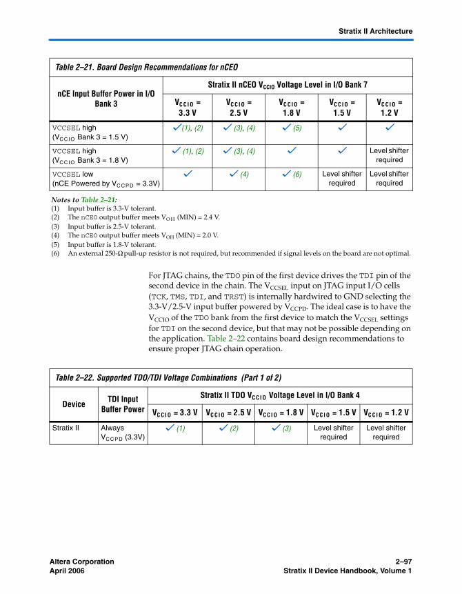
Altera Corporation 2–97April 2006 Stratix II Device Handbook, Volume 1
Stratix II Architecture
For JTAG chains, the TDO pin of the first device drives the TDI pin of the second device in the chain. The VCCSEL input on JTAG input I/O cells (TCK, TMS, TDI, and TRST) is internally hardwired to GND selecting the 3.3-V/2.5-V input buffer powered by VCCPD. The ideal case is to have the VCCIO of the TDO bank from the first device to match the VCCSEL settings for TDI on the second device, but that may not be possible depending on the application. Table 2–22 contains board design recommendations to ensure proper JTAG chain operation.
Table 2–21. Board Design Recommendations for nCEO
nCE Input Buffer Power in I/O Bank 3
Stratix II nCEO VCCIO Voltage Level in I/O Bank 7
VC C I O = 3.3 V
VC C I O =2.5 V
VC C I O =1.8 V
VC C I O =1.5 V
VC C I O =1.2 V
VCCSEL high (VC C I O Bank 3 = 1.5 V)
v(1), (2) v (3), (4) v (5) v v
VCCSEL high (VC C I O Bank 3 = 1.8 V)
v (1), (2) v (3), (4) v v Level shifter required
VCCSEL low (nCE Powered by VC CP D = 3.3V)
v v (4) v (6) Level shifter required
Level shifter required
Notes to Table 2–21:(1) Input buffer is 3.3-V tolerant.(2) The nCEO output buffer meets VO H (MIN) = 2.4 V.(3) Input buffer is 2.5-V tolerant.(4) The nCEO output buffer meets VOH (MIN) = 2.0 V.(5) Input buffer is 1.8-V tolerant.(6) An external 250-Ω pull-up resistor is not required, but recommended if signal levels on the board are not optimal.
Table 2–22. Supported TDO/TDI Voltage Combinations (Part 1 of 2)
Device TDI Input Buffer Power
Stratix II TDO VC C I O Voltage Level in I/O Bank 4
VC C I O = 3.3 V VC C I O = 2.5 V VC C I O = 1.8 V VC C I O = 1.5 V VC C I O = 1.2 V
Stratix II Always VC C P D (3.3V)
v (1) v (2) v (3) Level shifter required
Level shifter required
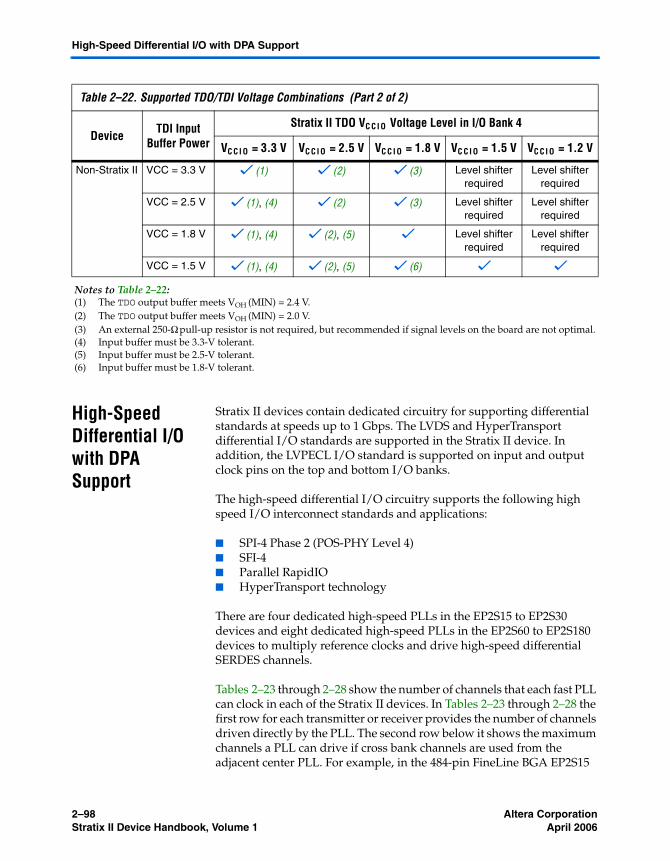
2–98 Altera CorporationStratix II Device Handbook, Volume 1 April 2006
High-Speed Differential I/O with DPA Support
High-Speed Differential I/O with DPA Support
Stratix II devices contain dedicated circuitry for supporting differential standards at speeds up to 1 Gbps. The LVDS and HyperTransport differential I/O standards are supported in the Stratix II device. In addition, the LVPECL I/O standard is supported on input and output clock pins on the top and bottom I/O banks.
The high-speed differential I/O circuitry supports the following high speed I/O interconnect standards and applications:
■ SPI-4 Phase 2 (POS-PHY Level 4)■ SFI-4■ Parallel RapidIO■ HyperTransport technology
There are four dedicated high-speed PLLs in the EP2S15 to EP2S30 devices and eight dedicated high-speed PLLs in the EP2S60 to EP2S180 devices to multiply reference clocks and drive high-speed differential SERDES channels.
Tables 2–23 through 2–28 show the number of channels that each fast PLL can clock in each of the Stratix II devices. In Tables 2–23 through 2–28 the first row for each transmitter or receiver provides the number of channels driven directly by the PLL. The second row below it shows the maximum channels a PLL can drive if cross bank channels are used from the adjacent center PLL. For example, in the 484-pin FineLine BGA EP2S15
Non-Stratix II VCC = 3.3 V v (1) v (2) v (3) Level shifter required
Level shifter required
VCC = 2.5 V v (1), (4) v (2) v (3) Level shifter required
Level shifter required
VCC = 1.8 V v (1), (4) v (2), (5) v Level shifter required
Level shifter required
VCC = 1.5 V v (1), (4) v (2), (5) v (6) v v
Notes to Table 2–22:(1) The TDO output buffer meets VOH (MIN) = 2.4 V.(2) The TDO output buffer meets VOH (MIN) = 2.0 V.(3) An external 250-Ω pull-up resistor is not required, but recommended if signal levels on the board are not optimal.(4) Input buffer must be 3.3-V tolerant.(5) Input buffer must be 2.5-V tolerant.(6) Input buffer must be 1.8-V tolerant.
Table 2–22. Supported TDO/TDI Voltage Combinations (Part 2 of 2)
Device TDI Input Buffer Power
Stratix II TDO VC C I O Voltage Level in I/O Bank 4
VC C I O = 3.3 V VC C I O = 2.5 V VC C I O = 1.8 V VC C I O = 1.5 V VC C I O = 1.2 V
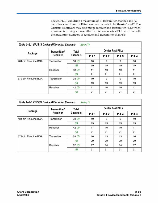
Altera Corporation 2–99April 2006 Stratix II Device Handbook, Volume 1
Stratix II Architecture
device, PLL 1 can drive a maximum of 10 transmitter channels in I/O bank 1 or a maximum of 19 transmitter channels in I/O banks 1 and 2. The Quartus II software may also merge receiver and transmitter PLLs when a receiver is driving a transmitter. In this case, one fast PLL can drive both the maximum numbers of receiver and transmitter channels.
Table 2–23. EP2S15 Device Differential Channels Note (1)
Package Transmitter/Receiver
Total Channels
Center Fast PLLs
PLL 1 PLL 2 PLL 3 PLL 4
484-pin FineLine BGA Transmitter 38 (2) 10 9 9 10
(3) 19 19 19 19
Receiver 42 (2) 11 10 10 11
(3) 21 21 21 21
672-pin FineLine BGA Transmitter 38 (2) 10 9 9 10
(3) 19 19 19 19
Receiver 42 (2) 11 10 10 11
(3) 21 21 21 21
Table 2–24. EP2S30 Device Differential Channels Note (1)
Package Transmitter/Receiver
Total Channels
Center Fast PLLs
PLL 1 PLL 2 PLL 3 PLL 4
484-pin FineLine BGA Transmitter 38 (2) 10 9 9 10
(3) 19 19 19 19
Receiver 42 (2) 11 10 10 11
(3) 21 21 21 21
672-pin FineLine BGA Transmitter 58 (2) 16 13 13 16
(3) 29 29 29 29
Receiver 62 (2) 17 14 14 17
(3) 31 31 31 31
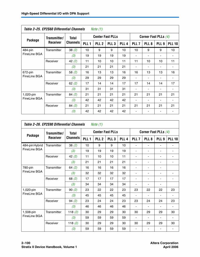
2–100 Altera CorporationStratix II Device Handbook, Volume 1 April 2006
High-Speed Differential I/O with DPA Support
Table 2–25. EP2S60 Differential Channels Note (1)
Package Transmitter/Receiver
Total Channels
Center Fast PLLs Corner Fast PLLs (4)
PLL 1 PLL 2 PLL 3 PLL 4 PLL 7 PLL 8 PLL 9 PLL 10
484-pin FineLine BGA
Transmitter 38 (2) 10 9 9 10 10 9 9 10
(3) 19 19 19 19 - - - -
Receiver 42 (2) 11 10 10 11 11 10 10 11
(3) 21 21 21 21 - - - -
672-pin FineLine BGA
Transmitter 58 (2) 16 13 13 16 16 13 13 16
(3) 29 29 29 29 - - - -
Receiver 62 (2) 17 14 14 17 17 14 14 17
(3) 31 31 31 31 - - - -
1,020-pin FineLine BGA
Transmitter 84 (2) 21 21 21 21 21 21 21 21
(3) 42 42 42 42 - - - -
Receiver 84 (2) 21 21 21 21 21 21 21 21
(3) 42 42 42 42 - - - -
Table 2–26. EP2S90 Differential Channels Note (1)
Package Transmitter/Receiver
Total Channels
Center Fast PLLs Corner Fast PLLs (4)
PLL 1 PLL 2 PLL 3 PLL 4 PLL 7 PLL 8 PLL 9 PLL 10
484-pin Hybrid FineLine BGA
Transmitter 38 (2) 10 9 9 10 - - - -
(3) 19 19 19 19 - - - -
Receiver 42 (2) 11 10 10 11 - - - -
(3) 21 21 21 21 - - - -
780-pin FineLine BGA
Transmitter 64 (2) 16 16 16 16 - - -
(3) 32 32 32 32 - - - -
Receiver 68 (2) 17 17 17 17 - - - -
(3) 34 34 34 34 - - -
1,020-pin FineLine BGA
Transmitter 90 (2) 23 22 22 23 23 22 22 23
(3) 45 45 45 45 - - - -
Receiver 94 (2) 23 24 24 23 23 24 24 23
(3) 46 46 46 46 - - - -
1,508-pin FineLine BGA
Transmitter 118 (2) 30 29 29 30 30 29 29 30
(3) 59 59 59 59 - - - -
Receiver 118 (2) 30 29 29 30 30 29 29 30
(3) 59 59 59 59 - - - -
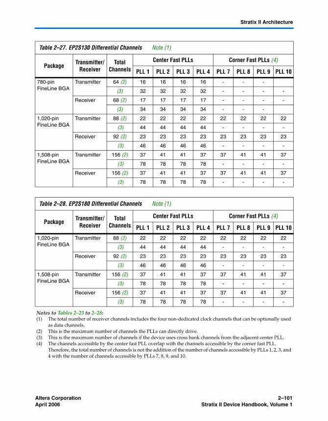
Altera Corporation 2–101April 2006 Stratix II Device Handbook, Volume 1
Stratix II Architecture
Table 2–27. EP2S130 Differential Channels Note (1)
Package Transmitter/Receiver
Total Channels
Center Fast PLLs Corner Fast PLLs (4)
PLL 1 PLL 2 PLL 3 PLL 4 PLL 7 PLL 8 PLL 9 PLL 10
780-pin FineLine BGA
Transmitter 64 (2) 16 16 16 16 - - -
(3) 32 32 32 32 - - - -
Receiver 68 (2) 17 17 17 17 - - - -
(3) 34 34 34 34 - - -
1,020-pin FineLine BGA
Transmitter 88 (2) 22 22 22 22 22 22 22 22
(3) 44 44 44 44 - - - -
Receiver 92 (2) 23 23 23 23 23 23 23 23
(3) 46 46 46 46 - - - -
1,508-pin FineLine BGA
Transmitter 156 (2) 37 41 41 37 37 41 41 37
(3) 78 78 78 78 - - - -
Receiver 156 (2) 37 41 41 37 37 41 41 37
(3) 78 78 78 78 - - - -
Table 2–28. EP2S180 Differential Channels Note (1)
Package Transmitter/Receiver
Total Channels
Center Fast PLLs Corner Fast PLLs (4)
PLL 1 PLL 2 PLL 3 PLL 4 PLL 7 PLL 8 PLL 9 PLL 10
1,020-pin FineLine BGA
Transmitter 88 (2) 22 22 22 22 22 22 22 22
(3) 44 44 44 44 - - - -
Receiver 92 (2) 23 23 23 23 23 23 23 23
(3) 46 46 46 46 - - - -
1,508-pin FineLine BGA
Transmitter 156 (2) 37 41 41 37 37 41 41 37
(3) 78 78 78 78 - - - -
Receiver 156 (2) 37 41 41 37 37 41 41 37
(3) 78 78 78 78 - - - -
Notes to Tables 2–23 to 2–28:(1) The total number of receiver channels includes the four non-dedicated clock channels that can be optionally used
as data channels.(2) This is the maximum number of channels the PLLs can directly drive.(3) This is the maximum number of channels if the device uses cross bank channels from the adjacent center PLL.(4) The channels accessible by the center fast PLL overlap with the channels accessible by the corner fast PLL.
Therefore, the total number of channels is not the addition of the number of channels accessible by PLLs 1, 2, 3, and 4 with the number of channels accessible by PLLs 7, 8, 9, and 10.
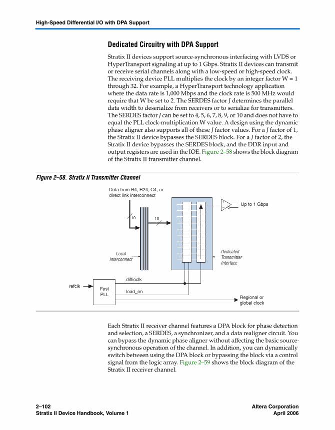
2–102 Altera CorporationStratix II Device Handbook, Volume 1 April 2006
High-Speed Differential I/O with DPA Support
Dedicated Circuitry with DPA Support
Stratix II devices support source-synchronous interfacing with LVDS or HyperTransport signaling at up to 1 Gbps. Stratix II devices can transmit or receive serial channels along with a low-speed or high-speed clock. The receiving device PLL multiplies the clock by an integer factor W = 1 through 32. For example, a HyperTransport technology application where the data rate is 1,000 Mbps and the clock rate is 500 MHz would require that W be set to 2. The SERDES factor J determines the parallel data width to deserialize from receivers or to serialize for transmitters. The SERDES factor J can be set to 4, 5, 6, 7, 8, 9, or 10 and does not have to equal the PLL clock-multiplication W value. A design using the dynamic phase aligner also supports all of these J factor values. For a J factor of 1, the Stratix II device bypasses the SERDES block. For a J factor of 2, the Stratix II device bypasses the SERDES block, and the DDR input and output registers are used in the IOE. Figure 2–58 shows the block diagram of the Stratix II transmitter channel.
Figure 2–58. Stratix II Transmitter Channel
Each Stratix II receiver channel features a DPA block for phase detection and selection, a SERDES, a synchronizer, and a data realigner circuit. You can bypass the dynamic phase aligner without affecting the basic source-synchronous operation of the channel. In addition, you can dynamically switch between using the DPA block or bypassing the block via a control signal from the logic array. Figure 2–59 shows the block diagram of the Stratix II receiver channel.
FastPLL
refclk
diffioclk
DedicatedTransmitterInterface
LocalInterconnect
10
+–
Up to 1 Gbps
load_enRegional orglobal clock
Data from R4, R24, C4, ordirect link interconnect
10
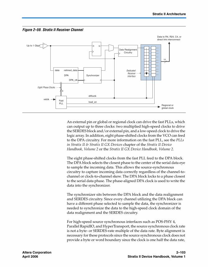
Altera Corporation 2–103April 2006 Stratix II Device Handbook, Volume 1
Stratix II Architecture
Figure 2–59. Stratix II Receiver Channel
An external pin or global or regional clock can drive the fast PLLs, which can output up to three clocks: two multiplied high-speed clocks to drive the SERDES block and/or external pin, and a low-speed clock to drive the logic array. In addition, eight phase-shifted clocks from the VCO can feed to the DPA circuitry. For more information on the fast PLL, see the PLLs in Stratix II & Stratix II GX Devices chapter of the Stratix II Device Handbook, Volume 2 or the Stratix II GX Device Handbook, Volume 2.
The eight phase-shifted clocks from the fast PLL feed to the DPA block. The DPA block selects the closest phase to the center of the serial data eye to sample the incoming data. This allows the source-synchronous circuitry to capture incoming data correctly regardless of the channel-to-channel or clock-to-channel skew. The DPA block locks to a phase closest to the serial data phase. The phase-aligned DPA clock is used to write the data into the synchronizer.
The synchronizer sits between the DPA block and the data realignment and SERDES circuitry. Since every channel utilizing the DPA block can have a different phase selected to sample the data, the synchronizer is needed to synchronize the data to the high-speed clock domain of the data realignment and the SERDES circuitry.
For high-speed source synchronous interfaces such as POS-PHY 4, Parallel RapidIO, and HyperTransport, the source synchronous clock rate is not a byte- or SERDES-rate multiple of the data rate. Byte alignment is necessary for these protocols since the source synchronous clock does not provide a byte or word boundary since the clock is one half the data rate,
+–
FastPLL
refclkload_en
diffioclk
Regional orglobal clock
Data to R4, R24, C4, ordirect link interconnect
Up to 1 Gbps
10
DedicatedReceiverInterface
Eight Phase Clocks
data retimed_data
DPA_clk
DPA Synchronizer
8
D Q
Data RealignmentCircuitry
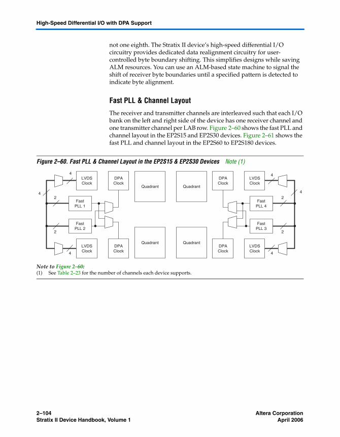
2–104 Altera CorporationStratix II Device Handbook, Volume 1 April 2006
High-Speed Differential I/O with DPA Support
not one eighth. The Stratix II device’s high-speed differential I/O circuitry provides dedicated data realignment circuitry for user-controlled byte boundary shifting. This simplifies designs while saving ALM resources. You can use an ALM-based state machine to signal the shift of receiver byte boundaries until a specified pattern is detected to indicate byte alignment.
Fast PLL & Channel Layout
The receiver and transmitter channels are interleaved such that each I/O bank on the left and right side of the device has one receiver channel and one transmitter channel per LAB row. Figure 2–60 shows the fast PLL and channel layout in the EP2S15 and EP2S30 devices. Figure 2–61 shows the fast PLL and channel layout in the EP2S60 to EP2S180 devices.
Figure 2–60. Fast PLL & Channel Layout in the EP2S15 & EP2S30 Devices Note (1)
Note to Figure 2–60:(1) See Table 2–23 for the number of channels each device supports.
LVDSClock
DPAClock
FastPLL 1
FastPLL 2
LVDSClock
DPAClock
LVDSClock
DPAClock
FastPLL 4
FastPLL 3
LVDSClock
DPAClock
Quadrant
Quadrant
Quadrant
Quadrant
4
4
4 4
4
42
2
2
2
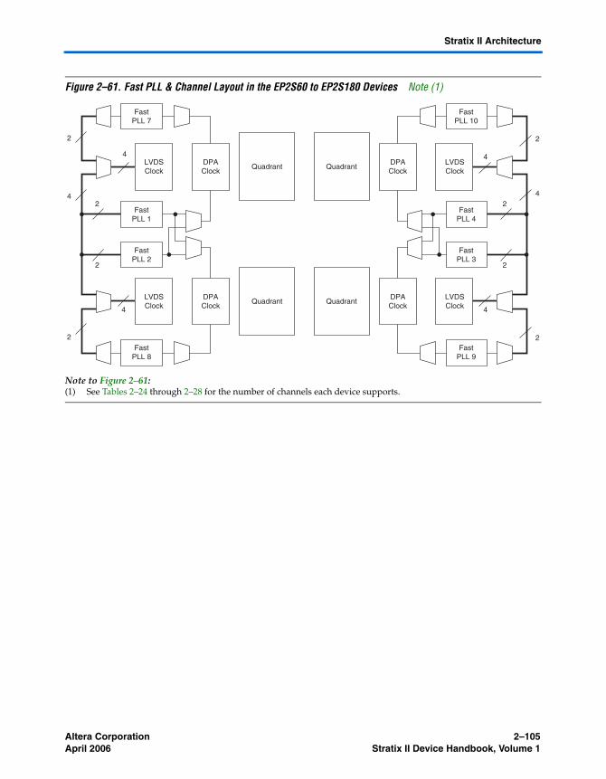
Altera Corporation 2–105April 2006 Stratix II Device Handbook, Volume 1
Stratix II Architecture
Figure 2–61. Fast PLL & Channel Layout in the EP2S60 to EP2S180 Devices Note (1)
Note to Figure 2–61:(1) See Tables 2–24 through 2–28 for the number of channels each device supports.
LVDSClock
DPAClock
FastPLL 1
FastPLL 2
LVDSClock
DPAClock
LVDSClock
DPAClock
FastPLL 4
FastPLL 7
FastPLL 10
FastPLL 3
LVDSClock
DPAClock
Quadrant
Quadrant
Quadrant
Quadrant
4
4
2
4 4
4
4
2
2
2
2
2
FastPLL 8
FastPLL 9
2 2
2–106 Altera CorporationStratix II Device Handbook, Volume 1 April 2006
High-Speed Differential I/O with DPA Support
Altera Corporation 3–1April 2006
3. Configuration & Testing
IEEE Std. 1149.1 JTAG Boundary-Scan Support
All Stratix® II devices provide Joint Test Action Group (JTAG) boundary-scan test (BST) circuitry that complies with the IEEE Std. 1149.1. JTAG boundary-scan testing can be performed either before or after, but not during configuration. Stratix II devices can also use the JTAG port for configuration with the Quartus® II software or hardware using either Jam Files (.jam) or Jam Byte-Code Files (.jbc).
Stratix II devices support IOE I/O standard setting reconfiguration through the JTAG BST chain. The JTAG chain can update the I/O standard for all input and output pins any time before or during user mode through the CONFIG_IO instruction. You can use this capability for JTAG testing before configuration when some of the Stratix II pins drive or receive from other devices on the board using voltage-referenced standards. Because the Stratix II device may not be configured before JTAG testing, the I/O pins may not be configured for appropriate electrical standards for chip-to-chip communication. Programming those I/O standards via JTAG allows you to fully test I/O connections to other devices.
A device operating in JTAG mode uses four required pins, TDI,TDO, TMS, and TCK, and one optional pin, TRST. The TCK pin has an internal weak pull-down resistor, while the TDI,TMS and TRST pins have weak internal pull-ups. The JTAG input pins are powered by the 3.3-V VCCPD pins. The TDO output pin is powered by the VCCIO power supply of bank 4.
Stratix II devices also use the JTAG port to monitor the logic operation of the device with the SignalTap® II embedded logic analyzer. Stratix II devices support the JTAG instructions shown in Table 3–1.
1 Stratix II, Stratix, Cyclone® II, and Cyclone devices must be within the first 17 devices in a JTAG chain. All of these devices have the same JTAG controller. If any of the Stratix II, Stratix, Cyclone II, or Cyclone devices are in the 18th of further position, they fail configuration. This does not affect SignalTap II.
The Stratix II device instruction register length is 10 bits and the USERCODE register length is 32 bits. Tables 3–2 and 3–3 show the boundary-scan register length and device IDCODE information for Stratix II devices.
SII51003-4.1
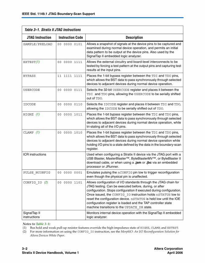
3–2 Altera CorporationStratix II Device Handbook, Volume 1 April 2006
IEEE Std. 1149.1 JTAG Boundary-Scan Support
Table 3–1. Stratix II JTAG Instructions
JTAG Instruction Instruction Code Description
SAMPLE/PRELOAD 00 0000 0101 Allows a snapshot of signals at the device pins to be captured and examined during normal device operation, and permits an initial data pattern to be output at the device pins. Also used by the SignalTap II embedded logic analyzer.
EXTEST(1) 00 0000 1111 Allows the external circuitry and board-level interconnects to be tested by forcing a test pattern at the output pins and capturing test results at the input pins.
BYPASS 11 1111 1111 Places the 1-bit bypass register between the TDI and TDO pins, which allows the BST data to pass synchronously through selected devices to adjacent devices during normal device operation.
USERCODE 00 0000 0111 Selects the 32-bit USERCODE register and places it between the TDI and TDO pins, allowing the USERCODE to be serially shifted out of TDO.
IDCODE 00 0000 0110 Selects the IDCODE register and places it between TDI and TDO, allowing the IDCODE to be serially shifted out of TDO.
HIGHZ (1) 00 0000 1011 Places the 1-bit bypass register between the TDI and TDO pins, which allows the BST data to pass synchronously through selected devices to adjacent devices during normal device operation, while tri-stating all of the I/O pins.
CLAMP (1) 00 0000 1010 Places the 1-bit bypass register between the TDI and TDO pins, which allows the BST data to pass synchronously through selected devices to adjacent devices during normal device operation while holding I/O pins to a state defined by the data in the boundary-scan register.
ICR instructions Used when configuring a Stratix II device via the JTAG port with a USB Blaster, MasterBlaster™, ByteBlasterMV™, or ByteBlaster II download cable, or when using a .jam or .jbc via an embedded processor or JRunner.
PULSE_NCONFIG 00 0000 0001 Emulates pulsing the nCONFIG pin low to trigger reconfiguration even though the physical pin is unaffected.
CONFIG_IO (2) 00 0000 1101 Allows configuration of I/O standards through the JTAG chain for JTAG testing. Can be executed before, during, or after configuration. Stops configuration if executed during configuration. Once issued, the CONFIG_IO instruction holds nSTATUS low to reset the configuration device. nSTATUS is held low until the IOE configuration register is loaded and the TAP controller state machine transitions to the UPDATE_DR state.
SignalTap II instructions
Monitors internal device operation with the SignalTap II embedded logic analyzer.
Notes to Table 3–1:(1) Bus hold and weak pull-up resistor features override the high-impedance state of HIGHZ, CLAMP, and EXTEST.(2) For more information on using the CONFIG_IO instruction, see the MorphIO: An I/O Reconfiguration Solution for
Altera Devices White Paper.
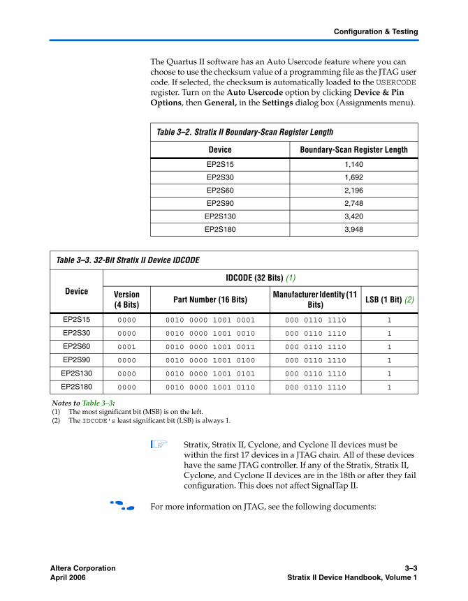
Altera Corporation 3–3April 2006 Stratix II Device Handbook, Volume 1
Configuration & Testing
The Quartus II software has an Auto Usercode feature where you can choose to use the checksum value of a programming file as the JTAG user code. If selected, the checksum is automatically loaded to the USERCODE register. Turn on the Auto Usercode option by clicking Device & Pin Options, then General, in the Settings dialog box (Assignments menu).
1 Stratix, Stratix II, Cyclone, and Cyclone II devices must be within the first 17 devices in a JTAG chain. All of these devices have the same JTAG controller. If any of the Stratix, Stratix II, Cyclone, and Cyclone II devices are in the 18th or after they fail configuration. This does not affect SignalTap II.
f For more information on JTAG, see the following documents:
Table 3–2. Stratix II Boundary-Scan Register Length
Device Boundary-Scan Register Length
EP2S15 1,140
EP2S30 1,692
EP2S60 2,196
EP2S90 2,748
EP2S130 3,420
EP2S180 3,948
Table 3–3. 32-Bit Stratix II Device IDCODE
Device
IDCODE (32 Bits) (1)
Version (4 Bits) Part Number (16 Bits) Manufacturer Identity (11
Bits) LSB (1 Bit) (2)
EP2S15 0000 0010 0000 1001 0001 000 0110 1110 1
EP2S30 0000 0010 0000 1001 0010 000 0110 1110 1
EP2S60 0001 0010 0000 1001 0011 000 0110 1110 1
EP2S90 0000 0010 0000 1001 0100 000 0110 1110 1
EP2S130 0000 0010 0000 1001 0101 000 0110 1110 1
EP2S180 0000 0010 0000 1001 0110 000 0110 1110 1
Notes to Table 3–3:(1) The most significant bit (MSB) is on the left.(2) The IDCODE's least significant bit (LSB) is always 1.
3–4 Altera CorporationStratix II Device Handbook, Volume 1 April 2006
SignalTap II Embedded Logic Analyzer
■ The IEEE Std. 1149.1 (JTAG) Boundary-Scan Testing for Stratix II & Stratix II GX Devices chapter of the Stratix II Device Handbook, Volume 2 or the Stratix II GX Device Handbook, Volume 2
■ Jam Programming & Test Language Specification
SignalTap II Embedded Logic Analyzer
Stratix II devices feature the SignalTap II embedded logic analyzer, which monitors design operation over a period of time through the IEEE Std. 1149.1 (JTAG) circuitry. You can analyze internal logic at speed without bringing internal signals to the I/O pins. This feature is particularly important for advanced packages, such as FineLine BGA® packages, because it can be difficult to add a connection to a pin during the debugging process after a board is designed and manufactured.
Configuration The logic, circuitry, and interconnects in the Stratix II architecture are configured with CMOS SRAM elements. Altera® FPGA devices are reconfigurable and every device is tested with a high coverage production test program so you do not have to perform fault testing and can instead focus on simulation and design verification.
Stratix II devices are configured at system power-up with data stored in an Altera configuration device or provided by an external controller (e.g., a MAX® II device or microprocessor). Stratix II devices can be configured using the fast passive parallel (FPP), active serial (AS), passive serial (PS), passive parallel asynchronous (PPA), and JTAG configuration schemes. The Stratix II device’s optimized interface allows microprocessors to configure it serially or in parallel, and synchronously or asynchronously. The interface also enables microprocessors to treat Stratix II devices as memory and configure them by writing to a virtual memory location, making reconfiguration easy.
In addition to the number of configuration methods supported, Stratix II devices also offer the design security, decompression, and remote system upgrade features. The design security feature, using configuration bitstream encryption and AES technology, provides a mechanism to protect your designs. The decompression feature allows Stratix II FPGAs to receive a compressed configuration bitstream and decompress this data in real-time, reducing storage requirements and configuration time. The remote system upgrade feature allows real-time system upgrades from remote locations of your Stratix II designs. For more information, see the “Configuration Schemes” section.
Altera Corporation 3–5April 2006 Stratix II Device Handbook, Volume 1
Configuration & Testing
Operating Modes
The Stratix II architecture uses SRAM configuration elements that require configuration data to be loaded each time the circuit powers up. The process of physically loading the SRAM data into the device is called configuration. During initialization, which occurs immediately after configuration, the device resets registers, enables I/O pins, and begins to operate as a logic device. The I/O pins are tri-stated during power-up, and before and during configuration. Together, the configuration and initialization processes are called command mode. Normal device operation is called user mode.
SRAM configuration elements allow Stratix II devices to be reconfigured in-circuit by loading new configuration data into the device. With real-time reconfiguration, the device is forced into command mode with a device pin. The configuration process loads different configuration data, reinitializes the device, and resumes user-mode operation. You can perform in-field upgrades by distributing new configuration files either within the system or remotely.
PORSEL is a dedicated input pin used to select POR delay times of 12 ms or 100 ms during power-up. When the PORSEL pin is connected to ground, the POR time is 100 ms; when the PORSEL pin is connected to VCC, the POR time is 12 ms.
The nIO PULLUP pin is a dedicated input that chooses whether the internal pull-ups on the user I/O pins and dual-purpose configuration I/O pins (nCSO, ASDO, DATA[7..0], nWS, nRS, RDYnBSY, nCS, CS, RUnLU, PGM[2..0], CLKUSR, INIT_DONE, DEV_OE, DEV_CLR) are on or off before and during configuration. A logic high (1.5, 1.8, 2.5, 3.3 V) turns off the weak internal pull-ups, while a logic low turns them on.
Stratix II devices also offer a new power supply, VCCPD, which must be connected to 3.3 V in order to power the 3.3-V/2.5-V buffer available on the configuration input pins and JTAG pins. VCCPD applies to all the JTAG input pins (TCK, TMS, TDI, and TRST) and the configuration input pins when VCCSEL is connected to ground. See Table 3–4 for more information on the pins affected by VCCSEL.
The VCCSEL pin allows the VCCIO setting (of the banks where the configuration inputs reside) to be independent of the voltage required by the configuration inputs. Therefore, when selecting the VCCIO, the VIL and VIH levels driven to the configuration inputs do not have to be a concern.
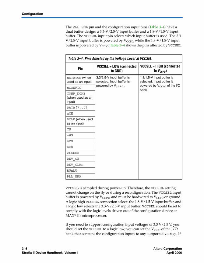
3–6 Altera CorporationStratix II Device Handbook, Volume 1 April 2006
Configuration
The PLL_ENA pin and the configuration input pins (Table 3–4) have a dual buffer design: a 3.3-V/2.5-V input buffer and a 1.8-V/1.5-V input buffer. The VCCSEL input pin selects which input buffer is used. The 3.3-V/2.5-V input buffer is powered by VCCPD, while the 1.8-V/1.5-V input buffer is powered by VCCIO. Table 3–4 shows the pins affected by VCCSEL.
VCCSEL is sampled during power-up. Therefore, the VCCSEL setting cannot change on the fly or during a reconfiguration. The VCCSEL input buffer is powered by VCCINT and must be hardwired to VCCPD or ground. A logic high VCCSEL connection selects the 1.8-V/1.5-V input buffer, and a logic low selects the 3.3-V/2.5-V input buffer. VCCSEL should be set to comply with the logic levels driven out of the configuration device or MAX® II/microprocessor.
If you need to support configuration input voltages of 3.3 V/2.5 V, you should set the VCCSEL to a logic low; you can set the VCCIO of the I/O bank that contains the configuration inputs to any supported voltage. If
Table 3–4. Pins Affected by the Voltage Level at VCCSEL
Pin VCCSEL = LOW (connected to GND)
VCCSEL = HIGH (connected to VCCPD)
nSTATUS (when used as an input)
3.3/2.5-V input buffer is selected. Input buffer is powered by VC C P D.
1.8/1.5-V input buffer is selected. Input buffer is powered by VC C I O of the I/O bank.
nCONFIG
CONF_DONE (when used as an input)
DATA[7..0]
nCE
DCLK (when used as an input)
CS
nWS
nRS
nCS
CLKUSR
DEV_OE
DEV_CLRn
RUnLU
PLL_ENA
Altera Corporation 3–7April 2006 Stratix II Device Handbook, Volume 1
Configuration & Testing
you need to support configuration input voltages of 1.8 V/1.5 V, you should set the VCCSEL to a logic high and the VCCIO of the bank that contains the configuration inputs to 1.8 V/1.5 V.
f For more information on multi-volt support, including information on using TDO and nCEO in multi-volt systems, refer to the Stratix II Architecture chapter of the Stratix II Device Handbook, Volume 1.
Configuration Schemes
You can load the configuration data for a Stratix II device with one of five configuration schemes (see Table 3–5), chosen on the basis of the target application. You can use a configuration device, intelligent controller, or the JTAG port to configure a Stratix II device. A configuration device can automatically configure a Stratix II device at system power-up.
You can configure multiple Stratix II devices in any of the five configuration schemes by connecting the configuration enable (nCE) and configuration enable output (nCEO) pins on each device.
Stratix II FPGAs offer the following:
■ Configuration data decompression to reduce configuration file storage
■ Design security using configuration data encryption to protect your designs
■ Remote system upgrades for remotely updating your Stratix II designs
Table 3–5 summarizes which configuration features can be used in each configuration scheme.
Table 3–5. Stratix II Configuration Features (Part 1 of 2)
Configuration Scheme Configuration Method Design Security Decompression Remote System
Upgrade
FPP MAX II device or microprocessor and flash device
v (1) v (1) v
Enhanced configuration device v (2) v
AS Serial configuration device v v v (3)
PS MAX II device or microprocessor and flash device
v v v
Enhanced configuration device v v v
Download cable (4) v v
3–8 Altera CorporationStratix II Device Handbook, Volume 1 April 2006
Configuration
See the Configuring Stratix II & Stratix II GX Devices chapter of the Stratix II Device Handbook, Volume 2 or the Stratix II GX Device Handbook, Volume 2 for more information about configuration schemes in Stratix II and Stratix II GX devices.
Device Security Using Configuration Bitstream Encryption
Stratix II FPGAs are the industry’s first FPGAs with the ability to decrypt a configuration bitstream using the Advanced Encryption Standard (AES) algorithm. When using the design security feature, a 128-bit security key is stored in the Stratix II FPGA. To successfully configure a Stratix II FPGA that has the design security feature enabled, it must be configured with a configuration file that was encrypted using the same 128-bit security key. The security key can be stored in non-volatile memory inside the Stratix II device. This non-volatile memory does not require any external devices, such as a battery back-up, for storage.
PPA MAX II device or microprocessor and flash device
v
JTAG Download cable (4)
MAX II device or microprocessor and flash device
Notes for Table 3–5:(1) In these modes, the host system must send a DCLK that is 4× the data rate.(2) The enhanced configuration device decompression feature is available, while the Stratix II decompression feature
is not available.(3) Only remote update mode is supported when using the AS configuration scheme. Local update mode is not
supported.(4) The supported download cables include the Altera USB Blaster universal serial bus (USB) port download cable,
MasterBlaster serial/USB communications cable, ByteBlaster II parallel port download cable, and the ByteBlasterMV parallel port download cable.
Table 3–5. Stratix II Configuration Features (Part 2 of 2)
Configuration Scheme Configuration Method Design Security Decompression Remote System
Upgrade
Altera Corporation 3–9April 2006 Stratix II Device Handbook, Volume 1
Configuration & Testing
1 An encryption configuration file is the same size as a non-encryption configuration file. When using a serial configuration scheme such as passive serial (PS) or active serial (AS), configuration time is the same whether or not the design security feature is enabled. If the fast passive parallel (FPP) scheme us used with the design security or decompression feature, a 4× DCLK is required. This results in a slower configuration time when compared to the configuration time of an FPGA that has neither the design security, nor decompression feature enabled. For more information about this feature, refer to AN 341: Using the Design Security Feature in Stratix II Devices. Contact your local Altera sales representative to request this document.
Device Configuration Data Decompression
Stratix II FPGAs support decompression of configuration data, which saves configuration memory space and time. This feature allows you to store compressed configuration data in configuration devices or other memory, and transmit this compressed bit stream to Stratix II FPGAs. During configuration, the Stratix II FPGA decompresses the bit stream in real time and programs its SRAM cells.
Stratix II FPGAs support decompression in the FPP (when using a MAX II device/microprocessor and flash memory), AS and PS configuration schemes. Decompression is not supported in the PPA configuration scheme nor in JTAG-based configuration.
Remote System Upgrades
Shortened design cycles, evolving standards, and system deployments in remote locations are difficult challenges faced by modern system designers. Stratix II devices can help effectively deal with these challenges with their inherent re-programmability and dedicated circuitry to perform remote system updates. Remote system updates help deliver feature enhancements and bug fixes without costly recalls, reduce time to market, and extend product life.
Stratix II FPGAs feature dedicated remote system upgrade circuitry to facilitate remote system updates. Soft logic (Nios® processor or user logic) implemented in the Stratix II device can download a new configuration image from a remote location, store it in configuration memory, and direct the dedicated remote system upgrade circuitry to initiate a reconfiguration cycle. The dedicated circuitry performs error detection during and after the configuration process, recovers from any error condition by reverting back to a safe configuration image, and provides
3–10 Altera CorporationStratix II Device Handbook, Volume 1 April 2006
Configuration
error status information. This dedicated remote system upgrade circuitry avoids system downtime and is the critical component for successful remote system upgrades.
RSC is supported in the following Stratix II configuration schemes: FPP, AS, PS, and PPA. RSC can also be implemented in conjunction with advanced Stratix II features such as real-time decompression of configuration data and design security using AES for secure and efficient field upgrades.
See the Remote System Upgrades With Stratix II & Stratix II GX Devices chapter of the Stratix II Device Handbook, Volume 2 or the Stratix II GX Device Handbook, Volume 2 for more information about remote configuration in Stratix II devices.
Configuring Stratix II FPGAs with JRunner
JRunner is a software driver that configures Altera FPGAs, including Stratix II FPGAs, through the ByteBlaster II or ByteBlasterMV cables in JTAG mode. The programming input file supported is in Raw Binary File (.rbf) format. JRunner also requires a Chain Description File (.cdf) generated by the Quartus II software. JRunner is targeted for embedded JTAG configuration. The source code is developed for the Windows NT operating system (OS), but can be customized to run on other platforms.
For more information on the JRunner software driver, see the JRunner Software Driver: An Embedded Solution to the JTAG Configuration White Paper and the source files on the Altera web site (www.altera.com).
Programming Serial Configuration Devices with SRunner
A serial configuration device can be programmed in-system by an external microprocessor using SRunner. SRunner is a software driver developed for embedded serial configuration device programming that can be easily customized to fit in different embedded systems. SRunner is able to read a .rpd file (Raw Programming Data) and write to the serial configuration devices. The serial configuration device programming time using SRunner is comparable to the programming time when using the Quartus II software.
For more information about SRunner, see the SRunner: An Embedded Solution for EPCS Programming White Paper and the source code on the Altera web site at www.altera.com.
For more information on programming serial configuration devices, see the Serial Configuration Devices (EPCS1 & EPCS4) Data Sheet in the Configuration Handbook.
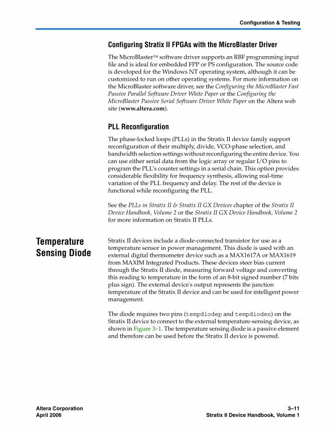
Altera Corporation 3–11April 2006 Stratix II Device Handbook, Volume 1
Configuration & Testing
Configuring Stratix II FPGAs with the MicroBlaster Driver
The MicroBlasterTM software driver supports an RBF programming input file and is ideal for embedded FPP or PS configuration. The source code is developed for the Windows NT operating system, although it can be customized to run on other operating systems. For more information on the MicroBlaster software driver, see the Configuring the MicroBlaster Fast Passive Parallel Software Driver White Paper or the Configuring the MicroBlaster Passive Serial Software Driver White Paper on the Altera web site (www.altera.com).
PLL Reconfiguration
The phase-locked loops (PLLs) in the Stratix II device family support reconfiguration of their multiply, divide, VCO-phase selection, and bandwidth selection settings without reconfiguring the entire device. You can use either serial data from the logic array or regular I/O pins to program the PLL’s counter settings in a serial chain. This option provides considerable flexibility for frequency synthesis, allowing real-time variation of the PLL frequency and delay. The rest of the device is functional while reconfiguring the PLL.
See the PLLs in Stratix II & Stratix II GX Devices chapter of the Stratix II Device Handbook, Volume 2 or the Stratix II GX Device Handbook, Volume 2 for more information on Stratix II PLLs.
Temperature Sensing Diode
Stratix II devices include a diode-connected transistor for use as a temperature sensor in power management. This diode is used with an external digital thermometer device such as a MAX1617A or MAX1619 from MAXIM Integrated Products. These devices steer bias current through the Stratix II diode, measuring forward voltage and converting this reading to temperature in the form of an 8-bit signed number (7 bits plus sign). The external device's output represents the junction temperature of the Stratix II device and can be used for intelligent power management.
The diode requires two pins (tempdiodep and tempdioden) on the Stratix II device to connect to the external temperature-sensing device, as shown in Figure 3–1. The temperature sensing diode is a passive element and therefore can be used before the Stratix II device is powered.
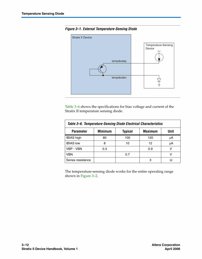
3–12 Altera CorporationStratix II Device Handbook, Volume 1 April 2006
Temperature Sensing Diode
Figure 3–1. External Temperature-Sensing Diode
Table 3–6 shows the specifications for bias voltage and current of the Stratix II temperature sensing diode.
The temperature-sensing diode works for the entire operating range shown in Figure 3–2.
Table 3–6. Temperature-Sensing Diode Electrical Characteristics
Parameter Minimum Typical Maximum Unit
IBIAS high 80 100 120 μA
IBIAS low 8 10 12 μA
VBP - VBN 0.3 0.9 V
VBN 0.7 V
Series resistance 3 Ω
Stratix II Device
Temperature-Sensing Device
tempdiodep
tempdioden
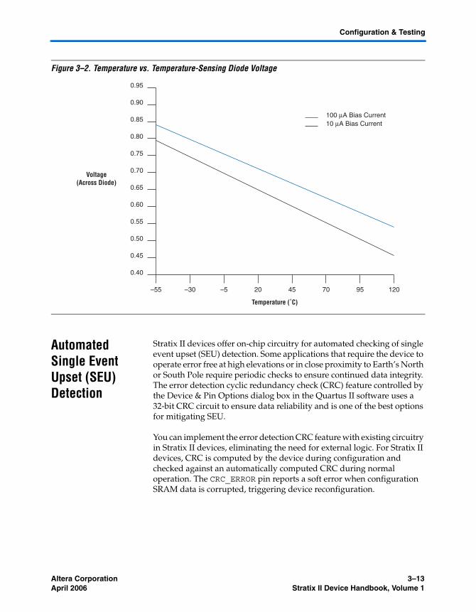
Altera Corporation 3–13April 2006 Stratix II Device Handbook, Volume 1
Configuration & Testing
Figure 3–2. Temperature vs. Temperature-Sensing Diode Voltage
Automated Single Event Upset (SEU) Detection
Stratix II devices offer on-chip circuitry for automated checking of single event upset (SEU) detection. Some applications that require the device to operate error free at high elevations or in close proximity to Earth’s North or South Pole require periodic checks to ensure continued data integrity. The error detection cyclic redundancy check (CRC) feature controlled by the Device & Pin Options dialog box in the Quartus II software uses a 32-bit CRC circuit to ensure data reliability and is one of the best options for mitigating SEU.
You can implement the error detection CRC feature with existing circuitry in Stratix II devices, eliminating the need for external logic. For Stratix II devices, CRC is computed by the device during configuration and checked against an automatically computed CRC during normal operation. The CRC_ERROR pin reports a soft error when configuration SRAM data is corrupted, triggering device reconfiguration.
0.90
0.85
0.95
0.75
0.65
Voltage(Across Diode)
Temperature (˚C)
0.55
0.45
0.60
0.50
0.40
0.70
0.80
–55 –30 –5 20 45 70 95 120
10 μA Bias Current100 μA Bias Current
3–14 Altera CorporationStratix II Device Handbook, Volume 1 April 2006
Automated Single Event Upset (SEU) Detection
Custom-Built Circuitry
Dedicated circuitry is built in the Stratix II devices to perform error detection automatically. This error detection circuitry in Stratix II devices constantly checks for errors in the configuration SRAM cells while the device is in user mode. You can monitor one external pin for the error and use it to trigger a re-configuration cycle. You can select the desired time between checks by adjusting a built-in clock divider.
Software Interface
In the Quartus II software version 4.1 and later, you can turn on the automated error detection CRC feature in the Device & Pin Options dialog box. This dialog box allows you to enable the feature and set the internal frequency of the CRC between 400 kHz to 50 MHz. This controls the rate that the CRC circuitry verifies the internal configuration SRAM bits in the FPGA device.
For more information on CRC, refer to AN 357: Error Detection Using CRC in Altera FPGA Devices.
Altera Corporation 4–1April 2006
4. Hot Socketing &Power-On Reset
Stratix® II devices offer hot socketing, which is also known as hot plug-in or hot swap, and power sequencing support without the use of any external devices. You can insert or remove a Stratix II board in a system during system operation without causing undesirable effects to the running system bus or the board that was inserted into the system.
The hot socketing feature also removes some of the difficulty when you use Stratix II devices on printed circuit boards (PCBs) that also contain a mixture of 5.0-, 3.3-, 2.5-, 1.8-, 1.5- and 1.2-V devices. With the Stratix II hot socketing feature, you no longer need to ensure a proper power-up sequence for each device on the board.
The Stratix II hot socketing feature provides:
■ Board or device insertion and removal without external components or board manipulation
■ Support for any power-up sequence■ Non-intrusive I/O buffers to system buses during hot insertion
This chapter also discusses the electro-static discharge (ESD) protection and the power-on reset (POR) circuitry in Stratix II devices. The POR circuitry keeps the devices in the reset state until the VCC is within operating range.
Stratix IIHot-Socketing Specifications
Stratix II devices offer hot socketing capability with all three features listed above without any external components or special design requirements. The hot socketing feature in Stratix II devices allows:
■ The device can be driven before power-up without any damage to the device itself.
■ I/O pins remain tri-stated during power-up. The device does not drive out before or during power-up, thereby affecting other buses in operation.
■ Signal pins do not drive the VCCIO, VCCPD, or VCCINT power supplies. External input signals to I/O pins of the device do not internally power the VCCIO or VCCINT power supplies of the device via internal paths within the device.
SII51004-3.1
4–2 Altera CorporationStratix II Device Handbook, Volume 1 April 2006
Stratix II Hot-Socketing Specifications
Devices Can Be Driven Before Power-Up
You can drive signals into the I/O pins, dedicated input pins and dedicated clock pins of Stratix II devices before or during power-up or power-down without damaging the device. Stratix II devices support any power-up or power-down sequence (VCCIO, VCCINT, and VCCPD) in order to simplify system level design.
I/O Pins Remain Tri-Stated During Power-Up
A device that does not support hot-socketing may interrupt system operation or cause contention by driving out before or during power-up. In a hot socketing situation, Stratix II device's output buffers are turned off during system power-up or power-down. Stratix II device also does not drive out until the device is configured and has attained proper operating conditions.
Signal Pins Do Not Drive the VCCIO, VCCINT or VCCPD Power Supplies
Devices that do not support hot-socketing can short power supplies together when powered-up through the device signal pins. This irregular power-up can damage both the driving and driven devices and can disrupt card power-up.
Stratix II devices do not have a current path from I/O pins, dedicated input pins, or dedicated clock pins to the VCCIO, VCCINT, or VCCPD pins before or during power-up. A Stratix II device may be inserted into (or removed from) a powered-up system board without damaging or interfering with system-board operation. When hot-socketing, Stratix II devices may have a minimal effect on the signal integrity of the backplane.
1 You can power up or power down the VCCIO, VCCINT, and VCCPD pins in any sequence. The power supply ramp rates can range from 100 μs to 100 ms. All VCC supplies must power down within 100 ms of each other to prevent I/O pins from driving out. During hot socketing, the I/O pin capacitance is less than 15 pF and the clock pin capacitance is less than 20 pF. Stratix II devices meet the following hot socketing specification.
■ The hot socketing DC specification is: | IIOPIN | < 300 μA.■ The hot socketing AC specification is: | IIOPIN | < 8 mA for 10 ns or
less.
Altera Corporation 4–3April 2006 Stratix II Device Handbook, Volume 1
Hot Socketing & Power-On Reset
IIOPIN is the current at any user I/O pin on the device. This specification takes into account the pin capacitance, but not board trace and external loading capacitance. Additional capacitance for trace, connector, and loading needs must be considered separately. For the AC specification, the peak current duration is 10 ns or less because of power-up transients. For more information, refer to the Hot-Socketing & Power-Sequencing Feature & Testing for Altera Devices white paper.
A possible concern regarding hot-socketing is the potential for latch-up. Latch-up can occur when electrical subsystems are hot-socketed into an active system. During hot-socketing, the signal pins may be connected and driven by the active system before the power supply can provide current to the device's VCC and ground planes. This condition can lead to latch-up and cause a low-impedance path from VCC to ground within the device. As a result, the device extends a large amount of current, possibly causing electrical damage. Nevertheless, Stratix II devices are immune to latch-up when hot-socketing.
Hot Socketing Feature Implementation in Stratix II Devices
The hot socketing feature turns off the output buffer during the power-up event (either VCCINT, VCCIO, or VCCPD supplies) or power down. The hot-socket circuit will generate an internal HOTSCKT signal when either VCCINT, VCCIO, or VCCPD is below threshold voltage. The HOTSCKT signal will cut off the output buffer to make sure that no DC current (except for weak pull up leaking) leaks through the pin. When VCC ramps up very slowly, VCC is still relatively low even after the POR signal is released and the configuration is finished. The CONF_DONE, nCEO, and nSTATUS pins fail to respond, as the output buffer can not flip from the state set by the hot socketing circuit at this low VCC voltage. Therefore, the hot socketing circuit has been removed on these configuration pins to make sure that they are able to operate during configuration. It is expected behavior for these pins to drive out during power-up and power-down sequences.
Each I/O pin has the following circuitry shown in Figure 4–1.
4–4 Altera CorporationStratix II Device Handbook, Volume 1 April 2006
Hot Socketing Feature Implementation in Stratix II Devices
Figure 4–1. Hot Socketing Circuit Block Diagram for Stratix II Devices
The POR circuit monitors VCCINT voltage level and keeps I/O pins tri-stated until the device is in user mode. The weak pull-up resistor (R) from the I/O pin to VCCIO is present to keep the I/O pins from floating. The 3.3-V tolerance control circuit permits the I/O pins to be driven by 3.3 V before VCCIO and/or VCCINT and/or VCCPD are powered, and it prevents the I/O pins from driving out when the device is not in user mode. The hot socket circuit prevents I/O pins from internally powering VCCIO, VCCINT, and VCCPD when driven by external signals before the device is powered.
Figure 4–2 shows a transistor level cross section of the Stratix II device I/O buffers. This design ensures that the output buffers do not drive when VCCIO is powered before VCCINT or if the I/O pad voltage is higher than VCCIO. This also applies for sudden voltage spikes during hot insertion. There is no current path from signal I/O pins to VCCINT or VCCIO or VCCPD during hot insertion. The VPAD leakage current charges the 3.3-V tolerant circuit capacitance.
Output Enable
Output
Hot Socket
OutputPre-Driver
VoltageTolerance
Control
Power OnReset
Monitor
WeakPull-Up
Resistor
PAD
Input Bufferto Logic Array
R
Altera Corporation 4–5April 2006 Stratix II Device Handbook, Volume 1
Hot Socketing & Power-On Reset
Figure 4–2. Transistor Level Diagram of FPGA Device I/O Buffers
Notes to Figure 4–2:(1) This is the logic array signal or the larger of either the VCCIO or VPAD signal.(2) This is the larger of either the VCCIO or VPAD signal.
Power-On Reset Circuitry
Stratix II devices have a POR circuit to keep the whole device system in reset state until the power supply voltage levels have stabilized during power-up. The POR circuit monitors the VCCINT, VCCIO, and VCCPD voltage levels and tri-states all the user I/O pins while VCC is ramping up until normal user levels are reached. The POR circuitry also ensures that all eight I/O bank VCCIO voltages, VCCPD voltage, as well as the logic array VCCINT voltage, reach an acceptable level before configuration is triggered. After the Stratix II device enters user mode, the POR circuit continues to monitor the VCCINT voltage level so that a brown-out condition during user mode can be detected. If there is a VCCINT voltage sag below the Stratix II operational level during user mode, the POR circuit resets the device.
When power is applied to a Stratix II device, a power-on-reset event occurs if VCC reaches the recommended operating range within a certain period of time (specified as a maximum VCC rise time). The maximum VCC rise time for Stratix II device is 100 ms. Stratix II devices provide a dedicated input pin (PORSEL) to select POR delay times of 12 or 100 ms during power-up. When the PORSEL pin is connected to ground, the POR time is 100 ms. When the PORSEL pin is connected to VCC, the POR time is 12 ms.
Logic ArraySignal (1) (2)
VCCIO
VPAD
n+ n+
n-well
n+p+p+
p-well
p-substrate
4–6 Altera CorporationStratix II Device Handbook, Volume 1 April 2006
Power-On Reset Circuitry
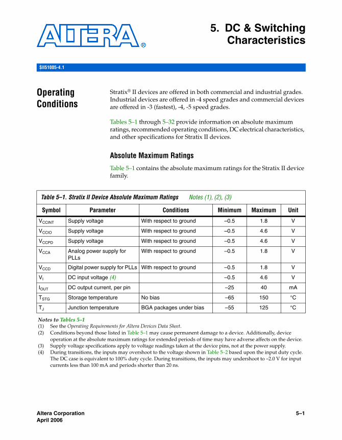
Altera Corporation 5–1April 2006
5. DC & SwitchingCharacteristics
Operating Conditions
Stratix® II devices are offered in both commercial and industrial grades. Industrial devices are offered in -4 speed grades and commercial devices are offered in -3 (fastest), -4, -5 speed grades.
Tables 5–1 through 5–32 provide information on absolute maximum ratings, recommended operating conditions, DC electrical characteristics, and other specifications for Stratix II devices.
Absolute Maximum Ratings
Table 5–1 contains the absolute maximum ratings for the Stratix II device family.
Table 5–1. Stratix II Device Absolute Maximum Ratings Notes (1), (2), (3)
Symbol Parameter Conditions Minimum Maximum Unit
VCCINT Supply voltage With respect to ground –0.5 1.8 V
VCCIO Supply voltage With respect to ground –0.5 4.6 V
VCCPD Supply voltage With respect to ground –0.5 4.6 V
VCCA Analog power supply for PLLs
With respect to ground –0.5 1.8 V
VCCD Digital power supply for PLLs With respect to ground –0.5 1.8 V
VI DC input voltage (4) –0.5 4.6 V
IOUT DC output current, per pin –25 40 mA
TSTG Storage temperature No bias –65 150 °C
TJ Junction temperature BGA packages under bias –55 125 °C
Notes to Tables 5–1(1) See the Operating Requirements for Altera Devices Data Sheet.(2) Conditions beyond those listed in Table 5–1 may cause permanent damage to a device. Additionally, device
operation at the absolute maximum ratings for extended periods of time may have adverse affects on the device.(3) Supply voltage specifications apply to voltage readings taken at the device pins, not at the power supply.(4) During transitions, the inputs may overshoot to the voltage shown in Table 5–2 based upon the input duty cycle.
The DC case is equivalent to 100% duty cycle. During transitions, the inputs may undershoot to –2.0 V for input currents less than 100 mA and periods shorter than 20 ns.
SII51005-4.1
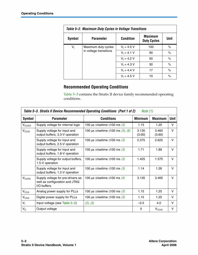
5–2 Altera CorporationStratix II Device Handbook, Volume 1 April 2006
Operating Conditions
Recommended Operating Conditions
Table 5–3 contains the Stratix II device family recommended operating conditions.
Table 5–2. Maximum Duty Cycles in Voltage Transitions
Symbol Parameter Condition Maximum Duty Cycles Unit
VI Maximum duty cycles in voltage transitions
VI = 4.0 V 100 %
VI = 4.1 V 90 %
VI = 4.2 V 50 %
VI = 4.3 V 30 %
VI = 4.4 V 17 %
VI = 4.5 V 10 %
Table 5–3. Stratix II Device Recommended Operating Conditions (Part 1 of 2) Note (1)
Symbol Parameter Conditions Minimum Maximum Unit
VCCINT Supply voltage for internal logic 100 μs ≤ risetime ≤ 100 ms (3) 1.15 1.25 V
VCCIO Supply voltage for input and output buffers, 3.3-V operation
100 μs ≤ risetime ≤ 100 ms (3), (6) 3.135 (3.00)
3.465 (3.60)
V
Supply voltage for input and output buffers, 2.5-V operation
100 μs ≤ risetime ≤ 100 ms (3) 2.375 2.625 V
Supply voltage for input and output buffers, 1.8-V operation
100 μs ≤ risetime ≤ 100 ms (3) 1.71 1.89 V
Supply voltage for output buffers, 1.5-V operation
100 μs ≤ risetime ≤ 100 ms (3) 1.425 1.575 V
Supply voltage for input and output buffers, 1.2-V operation
100 μs ≤ risetime ≤ 100 ms (3) 1.14 1.26 V
VCCPD Supply voltage for pre-drivers as well as configuration and JTAG I/O buffers.
100 μs ≤ risetime ≤ 100 ms (4) 3.135 3.465 V
VCCA Analog power supply for PLLs 100 μs ≤ risetime ≤ 100 ms (3) 1.15 1.25 V
VCCD Digital power supply for PLLs 100 μs ≤ risetime ≤ 100 ms (3) 1.15 1.25 V
VI Input voltage (see Table 5–2) (2), (5) –0.5 4.0 V
VO Output voltage 0 VCCIO V
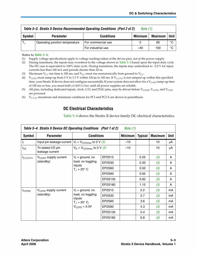
Altera Corporation 5–3April 2006 Stratix II Device Handbook, Volume 1
DC & Switching Characteristics
DC Electrical Characteristics
Table 5–4 shows the Stratix II device family DC electrical characteristics.
TJ Operating junction temperature For commercial use 0 85 °C
For industrial use –40 100 °C
Notes to Table 5–3:(1) Supply voltage specifications apply to voltage readings taken at the device pins, not at the power supply.(2) During transitions, the inputs may overshoot to the voltage shown in Table 5–2 based upon the input duty cycle.
The DC case is equivalent to 100% duty cycle. During transitions, the inputs may undershoot to –2.0 V for input currents less than 100 mA and periods shorter than 20 ns.
(3) Maximum VCC rise time is 100 ms, and VCC must rise monotonically from ground to VC C .(4) VCCPD must ramp-up from 0 V to 3.3 V within 100 μs to 100 ms. If VC C P D is not ramped up within this specified
time, your Stratix II device does not configure successfully. If your system does not allow for a VCCPD ramp-up time of 100 ms or less, you must hold nCONFIG low until all power supplies are reliable.
(5) All pins, including dedicated inputs, clock, I/O, and JTAG pins, may be driven before VCCINT, VCCPD, and VCCIO are powered.
(6) VC C I O maximum and minimum conditions for PCI and PCI-X are shown in parentheses.
Table 5–3. Stratix II Device Recommended Operating Conditions (Part 2 of 2) Note (1)
Symbol Parameter Conditions Minimum Maximum Unit
Table 5–4. Stratix II Device DC Operating Conditions (Part 1 of 2) Note (1)
Symbol Parameter Conditions Minimum Typical Maximum Unit
II Input pin leakage current VI = VCCIOmax to 0 V (2) –10 10 μA
IOZ Tri-stated I/O pin leakage current
VO = VCCIOmax to 0 V (2) –10 10 μA
IC CI NT 0 VCCINT supply current (standby)
VI = ground, no load, no toggling inputsTJ = 25° C
EP2S15 0.25 (3) A
EP2S30 0.30 (3) A
EP2S60 0.50 (3) A
EP2S90 0.62 (3) A
EP2S130 0.82 (3) A
EP2S180 1.12 (3) A
ICCPD0 VCCPD supply current (standby)
VI = ground, no load, no toggling inputsTJ = 25° C, VCCPD = 3.3V
EP2S15 2.2 (3) mA
EP2S30 2.7 (3) mA
EP2S60 3.6 (3) mA
EP2S90 4.3 (3) mA
EP2S130 5.4 (3) mA
EP2S180 6.8 (3) mA
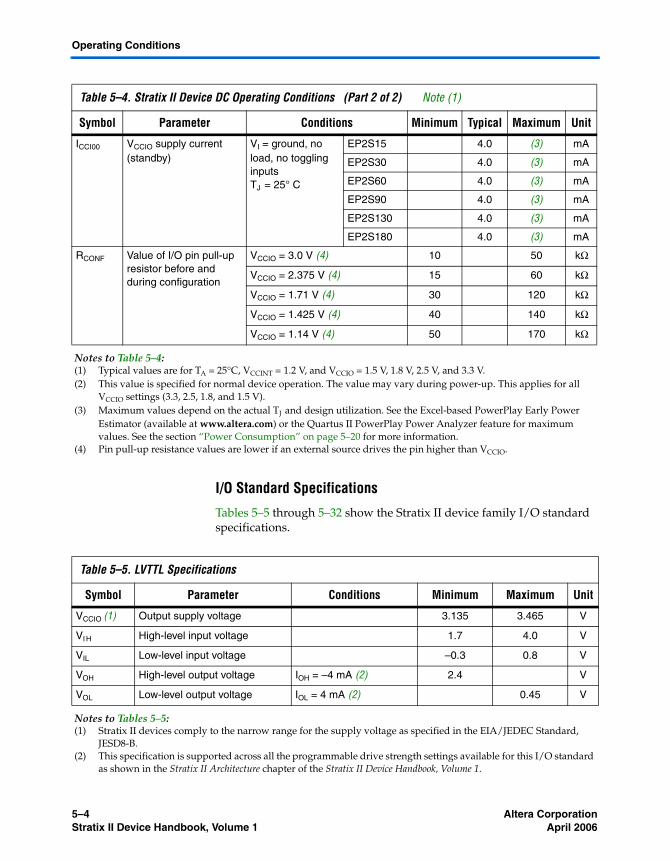
5–4 Altera CorporationStratix II Device Handbook, Volume 1 April 2006
Operating Conditions
I/O Standard Specifications
Tables 5–5 through 5–32 show the Stratix II device family I/O standard specifications.
ICCI00 VCCIO supply current (standby)
VI = ground, no load, no toggling inputsTJ = 25° C
EP2S15 4.0 (3) mA
EP2S30 4.0 (3) mA
EP2S60 4.0 (3) mA
EP2S90 4.0 (3) mA
EP2S130 4.0 (3) mA
EP2S180 4.0 (3) mA
RCONF Value of I/O pin pull-up resistor before and during configuration
VCCIO = 3.0 V (4) 10 50 kΩ
VCCIO = 2.375 V (4) 15 60 kΩ
VCCIO = 1.71 V (4) 30 120 kΩ
VCCIO = 1.425 V (4) 40 140 kΩ
VCCIO = 1.14 V (4) 50 170 kΩ
Notes to Table 5–4:(1) Typical values are for TA = 25°C, VCCINT = 1.2 V, and VCCIO = 1.5 V, 1.8 V, 2.5 V, and 3.3 V.(2) This value is specified for normal device operation. The value may vary during power-up. This applies for all
VCCIO settings (3.3, 2.5, 1.8, and 1.5 V).(3) Maximum values depend on the actual TJ and design utilization. See the Excel-based PowerPlay Early Power
Estimator (available at www.altera.com) or the Quartus II PowerPlay Power Analyzer feature for maximum values. See the section “Power Consumption” on page 5–20 for more information.
(4) Pin pull-up resistance values are lower if an external source drives the pin higher than VCCIO.
Table 5–4. Stratix II Device DC Operating Conditions (Part 2 of 2) Note (1)
Symbol Parameter Conditions Minimum Typical Maximum Unit
Table 5–5. LVTTL Specifications
Symbol Parameter Conditions Minimum Maximum Unit
VCCIO (1) Output supply voltage 3.135 3.465 V
VI H High-level input voltage 1.7 4.0 V
VIL Low-level input voltage –0.3 0.8 V
VOH High-level output voltage IOH = –4 mA (2) 2.4 V
VOL Low-level output voltage IOL = 4 mA (2) 0.45 V
Notes to Tables 5–5:(1) Stratix II devices comply to the narrow range for the supply voltage as specified in the EIA/JEDEC Standard,
JESD8-B.(2) This specification is supported across all the programmable drive strength settings available for this I/O standard
as shown in the Stratix II Architecture chapter of the Stratix II Device Handbook, Volume 1.
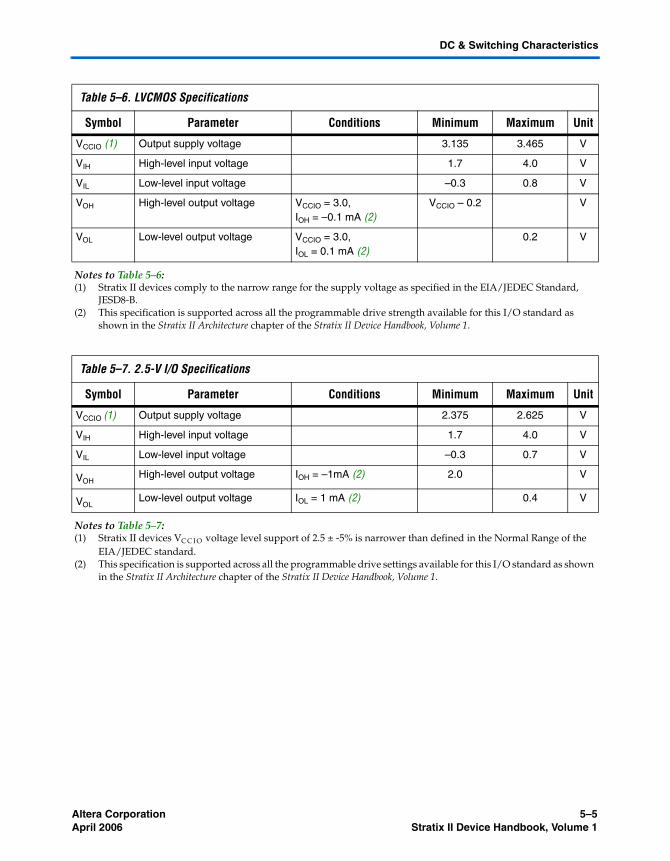
Altera Corporation 5–5April 2006 Stratix II Device Handbook, Volume 1
DC & Switching Characteristics
Table 5–6. LVCMOS Specifications
Symbol Parameter Conditions Minimum Maximum Unit
VCCIO (1) Output supply voltage 3.135 3.465 V
VIH High-level input voltage 1.7 4.0 V
VIL Low-level input voltage –0.3 0.8 V
VOH High-level output voltage VCCIO = 3.0, IOH = –0.1 mA (2)
VCCIO – 0.2 V
VOL Low-level output voltage VCCIO = 3.0,IOL = 0.1 mA (2)
0.2 V
Notes to Table 5–6:(1) Stratix II devices comply to the narrow range for the supply voltage as specified in the EIA/JEDEC Standard,
JESD8-B.(2) This specification is supported across all the programmable drive strength available for this I/O standard as
shown in the Stratix II Architecture chapter of the Stratix II Device Handbook, Volume 1.
Table 5–7. 2.5-V I/O Specifications
Symbol Parameter Conditions Minimum Maximum Unit
VCCIO (1) Output supply voltage 2.375 2.625 V
VIH High-level input voltage 1.7 4.0 V
VIL Low-level input voltage –0.3 0.7 V
VOHHigh-level output voltage IOH = –1mA (2) 2.0 V
VOLLow-level output voltage IOL = 1 mA (2) 0.4 V
Notes to Table 5–7:(1) Stratix II devices VC C I O voltage level support of 2.5 ± -5% is narrower than defined in the Normal Range of the
EIA/JEDEC standard.(2) This specification is supported across all the programmable drive settings available for this I/O standard as shown
in the Stratix II Architecture chapter of the Stratix II Device Handbook, Volume 1.
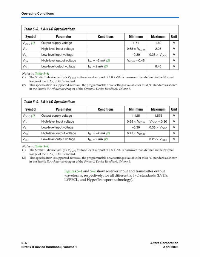
5–6 Altera CorporationStratix II Device Handbook, Volume 1 April 2006
Operating Conditions
Figures 5–1 and 5–2 show receiver input and transmitter output waveforms, respectively, for all differential I/O standards (LVDS, LVPECL, and HyperTransport technology).
Table 5–8. 1.8-V I/O Specifications
Symbol Parameter Conditions Minimum Maximum Unit
VCCIO (1) Output supply voltage 1.71 1.89 V
VI H High-level input voltage 0.65 × VCCIO 2.25 V
VIL Low-level input voltage –0.30 0.35 × VCCIO V
VOH High-level output voltage IOH = –2 mA (2) VCCIO – 0.45 V
VOL Low-level output voltage IOL = 2 mA (2) 0.45 V
Notes to Table 5–8:(1) The Stratix II device family’s VC C I O voltage level support of 1.8 ± -5% is narrower than defined in the Normal
Range of the EIA/JEDEC standard.(2) This specification is supported across all the programmable drive settings available for this I/O standard as shown
in the Stratix II Architecture chapter of the Stratix II Device Handbook, Volume 1.
Table 5–9. 1.5-V I/O Specifications
Symbol Parameter Conditions Minimum Maximum Unit
VCCIO (1) Output supply voltage 1.425 1.575 V
VI H High-level input voltage 0.65 × VCCIO VCCIO + 0.30 V
VIL Low-level input voltage –0.30 0.35 × VCCIO V
VOH High-level output voltage IOH = –2 mA (2) 0.75 × VCCIO V
VOL Low-level output voltage IOL = 2 mA (2) 0.25 × VCCIO V
Notes to Table 5–9:(1) The Stratix II device family’s VC C I O voltage level support of 1.5 ± -5% is narrower than defined in the Normal
Range of the EIA/JEDEC standard.(2) This specification is supported across all the programmable drive settings available for this I/O standard as shown
in the Stratix II Architecture chapter of the Stratix II Device Handbook, Volume 1.
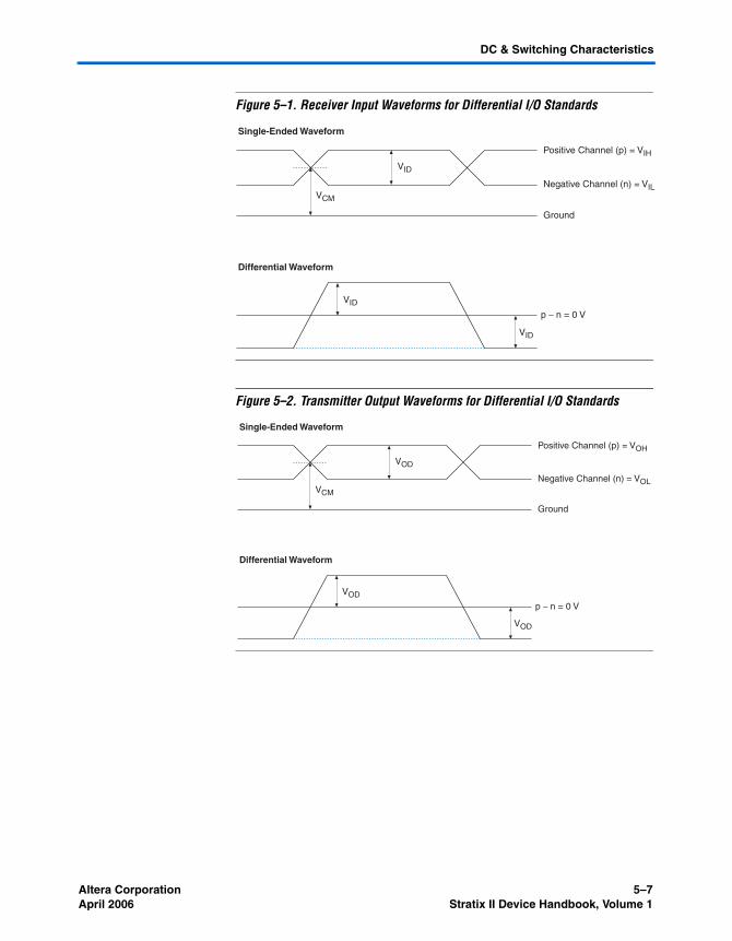
Altera Corporation 5–7April 2006 Stratix II Device Handbook, Volume 1
DC & Switching Characteristics
Figure 5–1. Receiver Input Waveforms for Differential I/O Standards
Figure 5–2. Transmitter Output Waveforms for Differential I/O Standards
Single-Ended Waveform
Differential Waveform
Positive Channel (p) = VIH
Negative Channel (n) = VIL
Ground
VID
VID
VID
p − n = 0 V
VCM
Single-Ended Waveform
Differential Waveform
Positive Channel (p) = VOH
Negative Channel (n) = VOL
Ground
VOD
VOD
VOD
p − n = 0 V
VCM
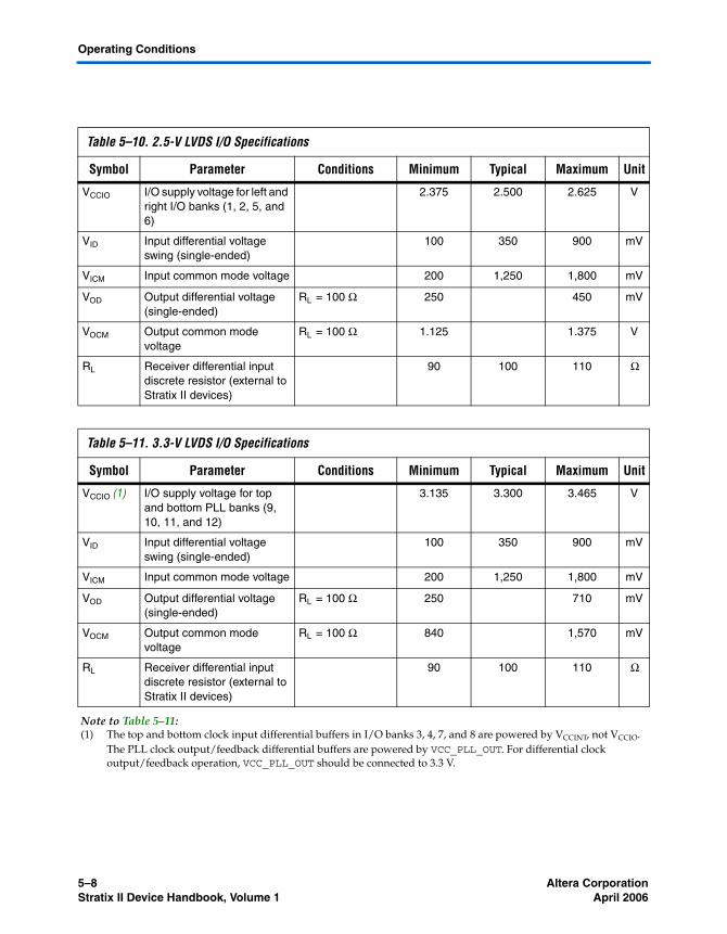
5–8 Altera CorporationStratix II Device Handbook, Volume 1 April 2006
Operating Conditions
Table 5–10. 2.5-V LVDS I/O Specifications
Symbol Parameter Conditions Minimum Typical Maximum Unit
VCCIO I/O supply voltage for left and right I/O banks (1, 2, 5, and 6)
2.375 2.500 2.625 V
VID Input differential voltage swing (single-ended)
100 350 900 mV
VICM Input common mode voltage 200 1,250 1,800 mV
VOD Output differential voltage (single-ended)
RL = 100 Ω 250 450 mV
VOCM Output common mode voltage
RL = 100 Ω 1.125 1.375 V
RL Receiver differential input discrete resistor (external to Stratix II devices)
90 100 110 Ω
Table 5–11. 3.3-V LVDS I/O Specifications
Symbol Parameter Conditions Minimum Typical Maximum Unit
VCCIO (1) I/O supply voltage for top and bottom PLL banks (9, 10, 11, and 12)
3.135 3.300 3.465 V
VID Input differential voltage swing (single-ended)
100 350 900 mV
VICM Input common mode voltage 200 1,250 1,800 mV
VOD Output differential voltage (single-ended)
RL = 100 Ω 250 710 mV
VOCM Output common mode voltage
RL = 100 Ω 840 1,570 mV
RL Receiver differential input discrete resistor (external to Stratix II devices)
90 100 110 Ω
Note to Table 5–11:(1) The top and bottom clock input differential buffers in I/O banks 3, 4, 7, and 8 are powered by VCCINT, not VCCIO.
The PLL clock output/feedback differential buffers are powered by VCC_PLL_OUT. For differential clock output/feedback operation, VCC_PLL_OUT should be connected to 3.3 V.
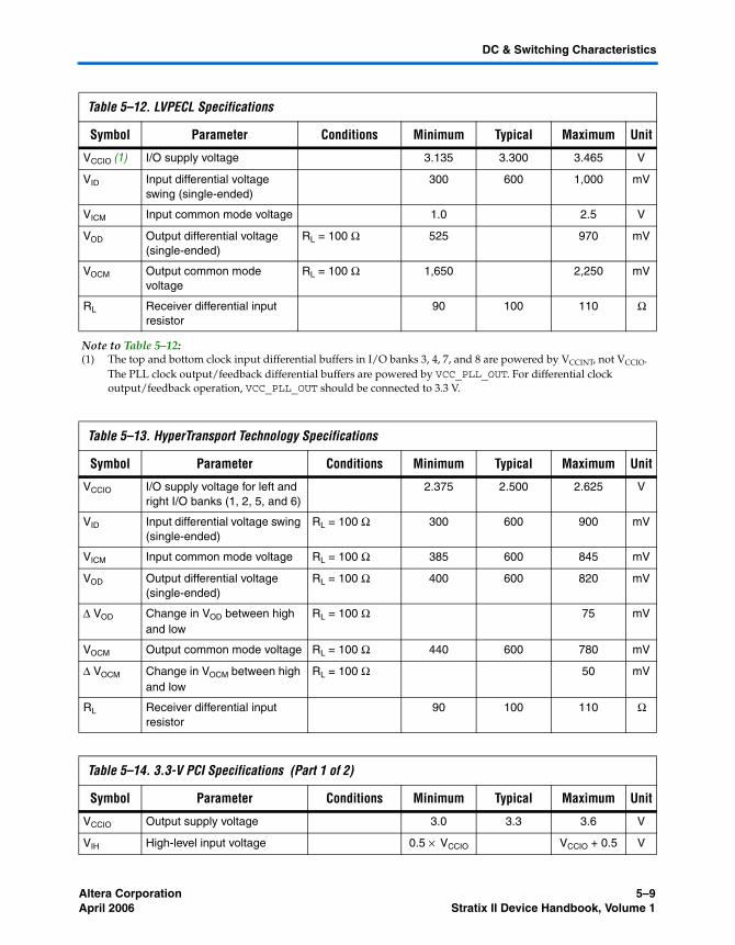
Altera Corporation 5–9April 2006 Stratix II Device Handbook, Volume 1
DC & Switching Characteristics
Table 5–12. LVPECL Specifications
Symbol Parameter Conditions Minimum Typical Maximum Unit
VCCIO (1) I/O supply voltage 3.135 3.300 3.465 V
VID Input differential voltage swing (single-ended)
300 600 1,000 mV
VICM Input common mode voltage 1.0 2.5 V
VOD Output differential voltage (single-ended)
RL = 100 Ω 525 970 mV
VOCM Output common mode voltage
RL = 100 Ω 1,650 2,250 mV
RL Receiver differential input resistor
90 100 110 Ω
Note to Table 5–12:(1) The top and bottom clock input differential buffers in I/O banks 3, 4, 7, and 8 are powered by VCCINT, not VCCIO.
The PLL clock output/feedback differential buffers are powered by VCC_PLL_OUT. For differential clock output/feedback operation, VCC_PLL_OUT should be connected to 3.3 V.
Table 5–13. HyperTransport Technology Specifications
Symbol Parameter Conditions Minimum Typical Maximum Unit
VCCIO I/O supply voltage for left and right I/O banks (1, 2, 5, and 6)
2.375 2.500 2.625 V
VID Input differential voltage swing (single-ended)
RL = 100 Ω 300 600 900 mV
VICM Input common mode voltage RL = 100 Ω 385 600 845 mV
VOD Output differential voltage (single-ended)
RL = 100 Ω 400 600 820 mV
Δ VOD Change in VOD between high and low
RL = 100 Ω 75 mV
VOCM Output common mode voltage RL = 100 Ω 440 600 780 mV
Δ VOCM Change in VOCM between high and low
RL = 100 Ω 50 mV
RL Receiver differential input resistor
90 100 110 Ω
Table 5–14. 3.3-V PCI Specifications (Part 1 of 2)
Symbol Parameter Conditions Minimum Typical Maximum Unit
VCCIO Output supply voltage 3.0 3.3 3.6 V
VIH High-level input voltage 0.5 × VCCIO VCCIO + 0.5 V
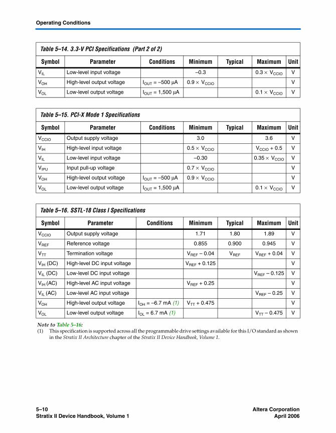
5–10 Altera CorporationStratix II Device Handbook, Volume 1 April 2006
Operating Conditions
VIL Low-level input voltage –0.3 0.3 × VCCIO V
VOH High-level output voltage IOUT = –500 μA 0.9 × VCCIO V
VOL Low-level output voltage IOUT = 1,500 μA 0.1 × VCCIO V
Table 5–15. PCI-X Mode 1 Specifications
Symbol Parameter Conditions Minimum Typical Maximum Unit
VCCIO Output supply voltage 3.0 3.6 V
VIH High-level input voltage 0.5 × VCCIO VCCIO + 0.5 V
VIL Low-level input voltage –0.30 0.35 × VCCIO V
VIPU Input pull-up voltage 0.7 × VCCIO V
VOH High-level output voltage IOUT = –500 μA 0.9 × VCCIO V
VOL Low-level output voltage IOUT = 1,500 μA 0.1 × VCCIO V
Table 5–16. SSTL-18 Class I Specifications
Symbol Parameter Conditions Minimum Typical Maximum Unit
VCCIO Output supply voltage 1.71 1.80 1.89 V
VREF Reference voltage 0.855 0.900 0.945 V
VTT Termination voltage VREF – 0.04 VREF VREF + 0.04 V
VIH (DC) High-level DC input voltage VREF + 0.125 V
VIL (DC) Low-level DC input voltage VREF – 0.125 V
VIH (AC) High-level AC input voltage VREF + 0.25 V
VIL (AC) Low-level AC input voltage VREF – 0.25 V
VOH High-level output voltage IOH = –6.7 mA (1) VTT + 0.475 V
VOL Low-level output voltage IOL = 6.7 mA (1) VTT – 0.475 V
Note to Table 5–16:(1) This specification is supported across all the programmable drive settings available for this I/O standard as shown
in the Stratix II Architecture chapter of the Stratix II Device Handbook, Volume 1.
Table 5–14. 3.3-V PCI Specifications (Part 2 of 2)
Symbol Parameter Conditions Minimum Typical Maximum Unit
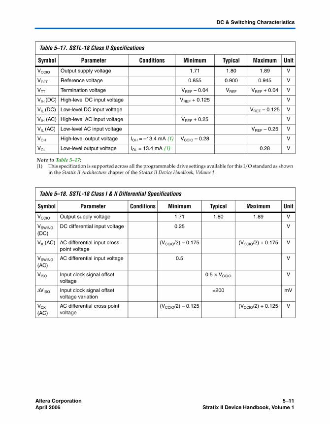
Altera Corporation 5–11April 2006 Stratix II Device Handbook, Volume 1
DC & Switching Characteristics
Table 5–17. SSTL-18 Class II Specifications
Symbol Parameter Conditions Minimum Typical Maximum Unit
VCCIO Output supply voltage 1.71 1.80 1.89 V
VREF Reference voltage 0.855 0.900 0.945 V
VTT Termination voltage VREF – 0.04 VREF VREF + 0.04 V
VIH (DC) High-level DC input voltage VREF + 0.125 V
VIL (DC) Low-level DC input voltage VREF – 0.125 V
VIH (AC) High-level AC input voltage VREF + 0.25 V
VIL (AC) Low-level AC input voltage VREF – 0.25 V
VOH High-level output voltage IOH = –13.4 mA (1) VCCIO – 0.28 V
VOL Low-level output voltage IOL = 13.4 mA (1) 0.28 V
Note to Table 5–17:(1) This specification is supported across all the programmable drive settings available for this I/O standard as shown
in the Stratix II Architecture chapter of the Stratix II Device Handbook, Volume 1.
Table 5–18. SSTL-18 Class I & II Differential Specifications
Symbol Parameter Conditions Minimum Typical Maximum Unit
VCCIO Output supply voltage 1.71 1.80 1.89 V
VSWING
(DC)DC differential input voltage 0.25 V
VX (AC) AC differential input cross point voltage
(VCCIO/2) – 0.175 (VCCIO/2) + 0.175 V
VSWING
(AC)AC differential input voltage 0.5 V
VISO Input clock signal offset voltage
0.5 × VCCIO V
ΔVISO Input clock signal offset voltage variation
±200 mV
VOX (AC)
AC differential cross point voltage
(VCCIO/2) – 0.125 (VCCIO/2) + 0.125 V
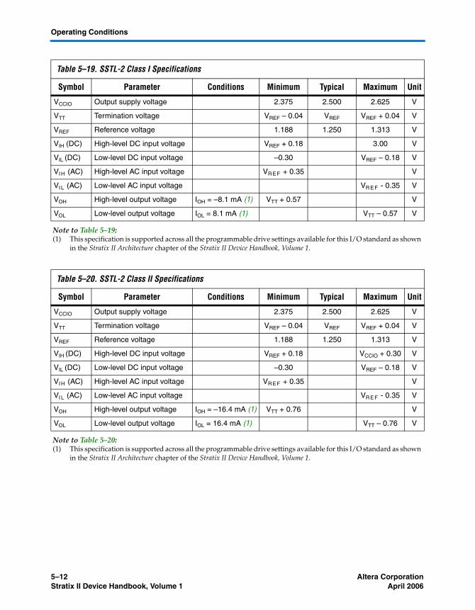
5–12 Altera CorporationStratix II Device Handbook, Volume 1 April 2006
Operating Conditions
Table 5–19. SSTL-2 Class I Specifications
Symbol Parameter Conditions Minimum Typical Maximum Unit
VCCIO Output supply voltage 2.375 2.500 2.625 V
VTT Termination voltage VREF – 0.04 VREF VREF + 0.04 V
VREF Reference voltage 1.188 1.250 1.313 V
VIH (DC) High-level DC input voltage VREF + 0.18 3.00 V
VIL (DC) Low-level DC input voltage –0.30 VREF – 0.18 V
VI H (AC) High-level AC input voltage VR E F + 0.35 V
VI L (AC) Low-level AC input voltage VR E F - 0.35 V
VOH High-level output voltage IOH = –8.1 mA (1) VTT + 0.57 V
VOL Low-level output voltage IOL = 8.1 mA (1) VTT – 0.57 V
Note to Table 5–19:(1) This specification is supported across all the programmable drive settings available for this I/O standard as shown
in the Stratix II Architecture chapter of the Stratix II Device Handbook, Volume 1.
Table 5–20. SSTL-2 Class II Specifications
Symbol Parameter Conditions Minimum Typical Maximum Unit
VCCIO Output supply voltage 2.375 2.500 2.625 V
VTT Termination voltage VREF – 0.04 VREF VREF + 0.04 V
VREF Reference voltage 1.188 1.250 1.313 V
VIH (DC) High-level DC input voltage VREF + 0.18 VCCIO + 0.30 V
VIL (DC) Low-level DC input voltage –0.30 VREF – 0.18 V
VI H (AC) High-level AC input voltage VR E F + 0.35 V
VI L (AC) Low-level AC input voltage VR E F - 0.35 V
VOH High-level output voltage IOH = –16.4 mA (1) VTT + 0.76 V
VOL Low-level output voltage IOL = 16.4 mA (1) VTT – 0.76 V
Note to Table 5–20:(1) This specification is supported across all the programmable drive settings available for this I/O standard as shown
in the Stratix II Architecture chapter of the Stratix II Device Handbook, Volume 1.
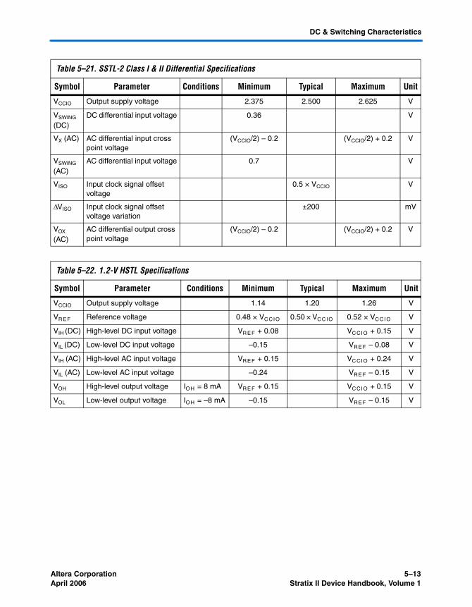
Altera Corporation 5–13April 2006 Stratix II Device Handbook, Volume 1
DC & Switching Characteristics
Table 5–21. SSTL-2 Class I & II Differential Specifications
Symbol Parameter Conditions Minimum Typical Maximum Unit
VCCIO Output supply voltage 2.375 2.500 2.625 V
VSWING
(DC)DC differential input voltage 0.36 V
VX (AC) AC differential input cross point voltage
(VCCIO/2) – 0.2 (VCCIO/2) + 0.2 V
VSWING
(AC)AC differential input voltage 0.7 V
VISO Input clock signal offset voltage
0.5 × VCCIO V
ΔVISO Input clock signal offset voltage variation
±200 mV
VOX (AC)
AC differential output cross point voltage
(VCCIO/2) – 0.2 (VCCIO/2) + 0.2 V
Table 5–22. 1.2-V HSTL Specifications
Symbol Parameter Conditions Minimum Typical Maximum Unit
VCCIO Output supply voltage 1.14 1.20 1.26 V
VRE F Reference voltage 0.48 × VC C I O 0.50 × VC C I O 0.52 × VC C I O V
VIH (DC) High-level DC input voltage VR E F + 0.08 VC CI O + 0.15 V
VIL (DC) Low-level DC input voltage –0.15 VR E F – 0.08 V
VIH (AC) High-level AC input voltage VR E F + 0.15 VC CI O + 0.24 V
VIL (AC) Low-level AC input voltage –0.24 VR E F – 0.15 V
VOH High-level output voltage IO H = 8 mA VR E F + 0.15 VC CI O + 0.15 V
VOL Low-level output voltage IO H = –8 mA –0.15 VR E F – 0.15 V
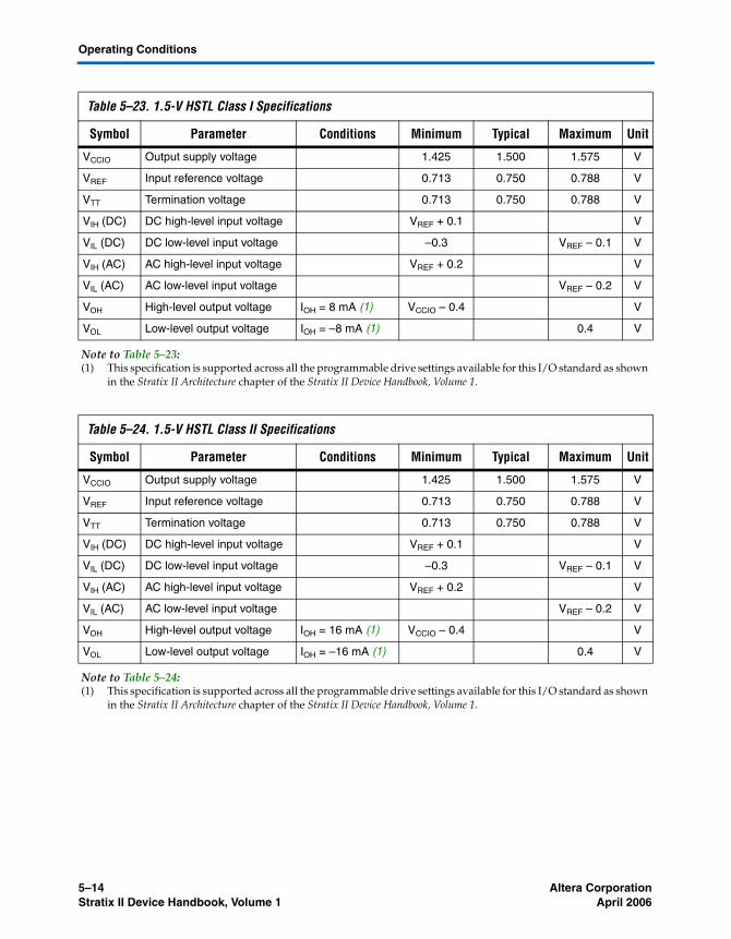
5–14 Altera CorporationStratix II Device Handbook, Volume 1 April 2006
Operating Conditions
Table 5–23. 1.5-V HSTL Class I Specifications
Symbol Parameter Conditions Minimum Typical Maximum Unit
VCCIO Output supply voltage 1.425 1.500 1.575 V
VREF Input reference voltage 0.713 0.750 0.788 V
VTT Termination voltage 0.713 0.750 0.788 V
VIH (DC) DC high-level input voltage VREF + 0.1 V
VIL (DC) DC low-level input voltage –0.3 VREF – 0.1 V
VIH (AC) AC high-level input voltage VREF + 0.2 V
VIL (AC) AC low-level input voltage VREF – 0.2 V
VOH High-level output voltage IOH = 8 mA (1) VCCIO – 0.4 V
VOL Low-level output voltage IOH = –8 mA (1) 0.4 V
Note to Table 5–23:(1) This specification is supported across all the programmable drive settings available for this I/O standard as shown
in the Stratix II Architecture chapter of the Stratix II Device Handbook, Volume 1.
Table 5–24. 1.5-V HSTL Class II Specifications
Symbol Parameter Conditions Minimum Typical Maximum Unit
VCCIO Output supply voltage 1.425 1.500 1.575 V
VREF Input reference voltage 0.713 0.750 0.788 V
VTT Termination voltage 0.713 0.750 0.788 V
VIH (DC) DC high-level input voltage VREF + 0.1 V
VIL (DC) DC low-level input voltage –0.3 VREF – 0.1 V
VIH (AC) AC high-level input voltage VREF + 0.2 V
VIL (AC) AC low-level input voltage VREF – 0.2 V
VOH High-level output voltage IOH = 16 mA (1) VCCIO – 0.4 V
VOL Low-level output voltage IOH = –16 mA (1) 0.4 V
Note to Table 5–24:(1) This specification is supported across all the programmable drive settings available for this I/O standard as shown
in the Stratix II Architecture chapter of the Stratix II Device Handbook, Volume 1.
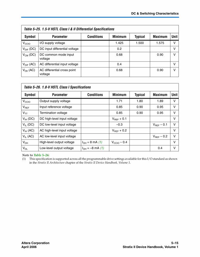
Altera Corporation 5–15April 2006 Stratix II Device Handbook, Volume 1
DC & Switching Characteristics
Table 5–25. 1.5-V HSTL Class I & II Differential Specifications
Symbol Parameter Conditions Minimum Typical Maximum Unit
VCCIO I/O supply voltage 1.425 1.500 1.575 V
VDIF (DC) DC input differential voltage 0.2 V
VCM (DC) DC common mode input voltage
0.68 0.90 V
VDIF (AC) AC differential input voltage 0.4 V
VOX (AC) AC differential cross point voltage
0.68 0.90 V
Table 5–26. 1.8-V HSTL Class I Specifications
Symbol Parameter Conditions Minimum Typical Maximum Unit
VCCIO Output supply voltage 1.71 1.80 1.89 V
VREF Input reference voltage 0.85 0.90 0.95 V
VTT Termination voltage 0.85 0.90 0.95 V
VIH (DC) DC high-level input voltage VREF + 0.1 V
VIL (DC) DC low-level input voltage –0.3 VREF – 0.1 V
VIH (AC) AC high-level input voltage VREF + 0.2 V
VIL (AC) AC low-level input voltage VREF – 0.2 V
VOH High-level output voltage IOH = 8 mA (1) VCCIO – 0.4 V
VOL Low-level output voltage IOH = –8 mA (1) 0.4 V
Note to Table 5–26:(1) This specification is supported across all the programmable drive settings available for this I/O standard as shown
in the Stratix II Architecture chapter of the Stratix II Device Handbook, Volume 1.
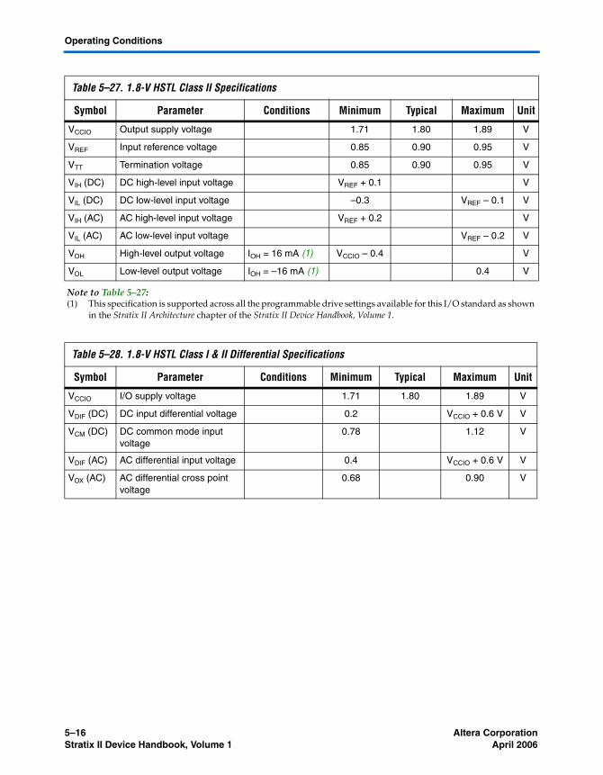
5–16 Altera CorporationStratix II Device Handbook, Volume 1 April 2006
Operating Conditions
Table 5–27. 1.8-V HSTL Class II Specifications
Symbol Parameter Conditions Minimum Typical Maximum Unit
VCCIO Output supply voltage 1.71 1.80 1.89 V
VREF Input reference voltage 0.85 0.90 0.95 V
VTT Termination voltage 0.85 0.90 0.95 V
VIH (DC) DC high-level input voltage VREF + 0.1 V
VIL (DC) DC low-level input voltage –0.3 VREF – 0.1 V
VIH (AC) AC high-level input voltage VREF + 0.2 V
VIL (AC) AC low-level input voltage VREF – 0.2 V
VOH High-level output voltage IOH = 16 mA (1) VCCIO – 0.4 V
VOL Low-level output voltage IOH = –16 mA (1) 0.4 V
Note to Table 5–27:(1) This specification is supported across all the programmable drive settings available for this I/O standard as shown
in the Stratix II Architecture chapter of the Stratix II Device Handbook, Volume 1.
Table 5–28. 1.8-V HSTL Class I & II Differential Specifications
Symbol Parameter Conditions Minimum Typical Maximum Unit
VCCIO I/O supply voltage 1.71 1.80 1.89 V
VDIF (DC) DC input differential voltage 0.2 VCCIO + 0.6 V V
VCM (DC) DC common mode input voltage
0.78 1.12 V
VDIF (AC) AC differential input voltage 0.4 VCCIO + 0.6 V V
VOX (AC) AC differential cross point voltage
0.68 0.90 V
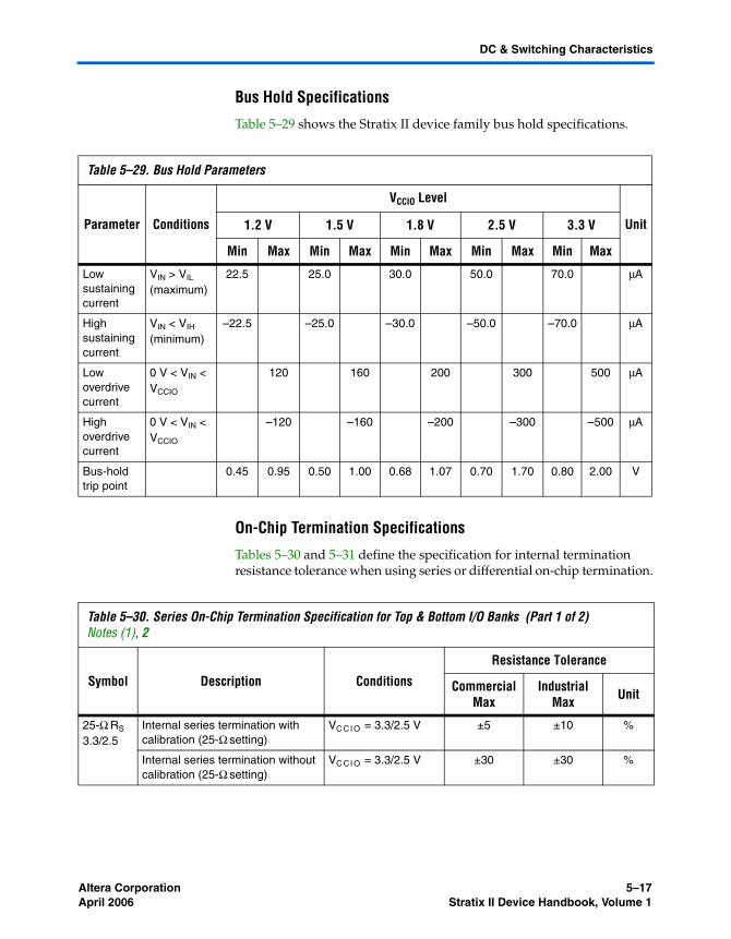
Altera Corporation 5–17April 2006 Stratix II Device Handbook, Volume 1
DC & Switching Characteristics
Bus Hold Specifications
Table 5–29 shows the Stratix II device family bus hold specifications.
On-Chip Termination Specifications
Tables 5–30 and 5–31 define the specification for internal termination resistance tolerance when using series or differential on-chip termination.
Table 5–29. Bus Hold Parameters
Parameter Conditions
VCCIO Level
Unit1.2 V 1.5 V 1.8 V 2.5 V 3.3 V
Min Max Min Max Min Max Min Max Min Max
Low sustaining current
VIN > VIL (maximum)
22.5 25.0 30.0 50.0 70.0 μA
High sustaining current
VIN < VIH (minimum)
–22.5 –25.0 –30.0 –50.0 –70.0 μA
Low overdrive current
0 V < VIN < VCCIO
120 160 200 300 500 μA
High overdrive current
0 V < VIN < VCCIO
–120 –160 –200 –300 –500 μA
Bus-hold trip point
0.45 0.95 0.50 1.00 0.68 1.07 0.70 1.70 0.80 2.00 V
Table 5–30. Series On-Chip Termination Specification for Top & Bottom I/O Banks (Part 1 of 2)Notes (1), 2
Symbol Description Conditions
Resistance Tolerance
Commercial Max
Industrial Max Unit
25-Ω RS 3.3/2.5
Internal series termination with calibration (25-Ω setting)
VC CI O = 3.3/2.5 V ±5 ±10 %
Internal series termination without calibration (25-Ω setting)
VC CI O = 3.3/2.5 V ±30 ±30 %
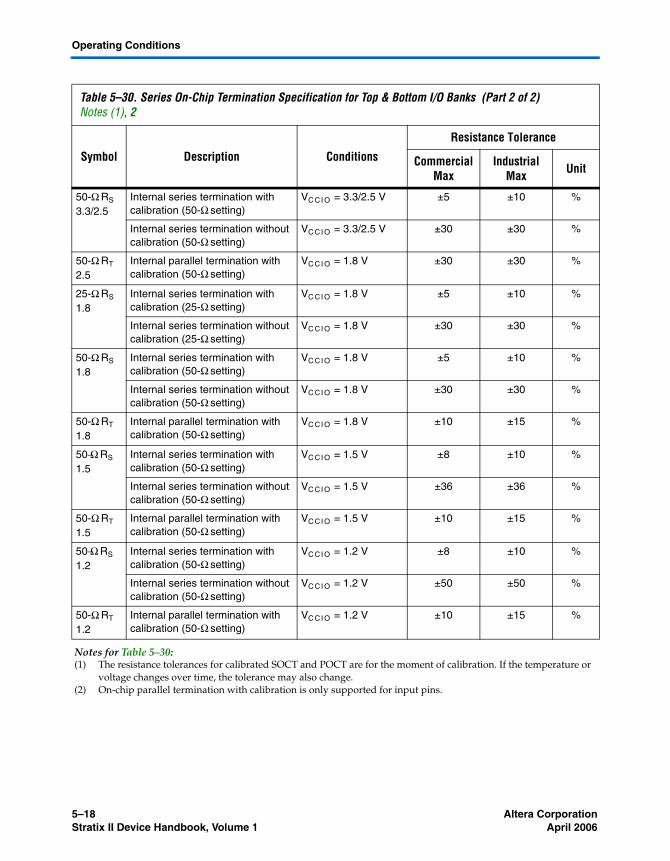
5–18 Altera CorporationStratix II Device Handbook, Volume 1 April 2006
Operating Conditions
50-Ω RS 3.3/2.5
Internal series termination with calibration (50-Ω setting)
VC CI O = 3.3/2.5 V ±5 ±10 %
Internal series termination without calibration (50-Ω setting)
VC CI O = 3.3/2.5 V ±30 ±30 %
50-Ω RT 2.5
Internal parallel termination with calibration (50-Ω setting)
VC CI O = 1.8 V ±30 ±30 %
25-Ω RS 1.8
Internal series termination with calibration (25-Ω setting)
VC CI O = 1.8 V ±5 ±10 %
Internal series termination without calibration (25-Ω setting)
VC CI O = 1.8 V ±30 ±30 %
50-Ω RS 1.8
Internal series termination with calibration (50-Ω setting)
VC CI O = 1.8 V ±5 ±10 %
Internal series termination without calibration (50-Ω setting)
VC CI O = 1.8 V ±30 ±30 %
50-Ω RT 1.8
Internal parallel termination with calibration (50-Ω setting)
VC CI O = 1.8 V ±10 ±15 %
50−Ω RS 1.5
Internal series termination with calibration (50-Ω setting)
VC CI O = 1.5 V ±8 ±10 %
Internal series termination without calibration (50-Ω setting)
VC CI O = 1.5 V ±36 ±36 %
50-Ω RT 1.5
Internal parallel termination with calibration (50-Ω setting)
VC CI O = 1.5 V ±10 ±15 %
50−Ω RS 1.2
Internal series termination with calibration (50-Ω setting)
VC CI O = 1.2 V ±8 ±10 %
Internal series termination without calibration (50-Ω setting)
VC CI O = 1.2 V ±50 ±50 %
50-Ω RT 1.2
Internal parallel termination with calibration (50-Ω setting)
VC CI O = 1.2 V ±10 ±15 %
Notes for Table 5–30:(1) The resistance tolerances for calibrated SOCT and POCT are for the moment of calibration. If the temperature or
voltage changes over time, the tolerance may also change.(2) On-chip parallel termination with calibration is only supported for input pins.
Table 5–30. Series On-Chip Termination Specification for Top & Bottom I/O Banks (Part 2 of 2)Notes (1), 2
Symbol Description Conditions
Resistance Tolerance
Commercial Max
Industrial Max Unit
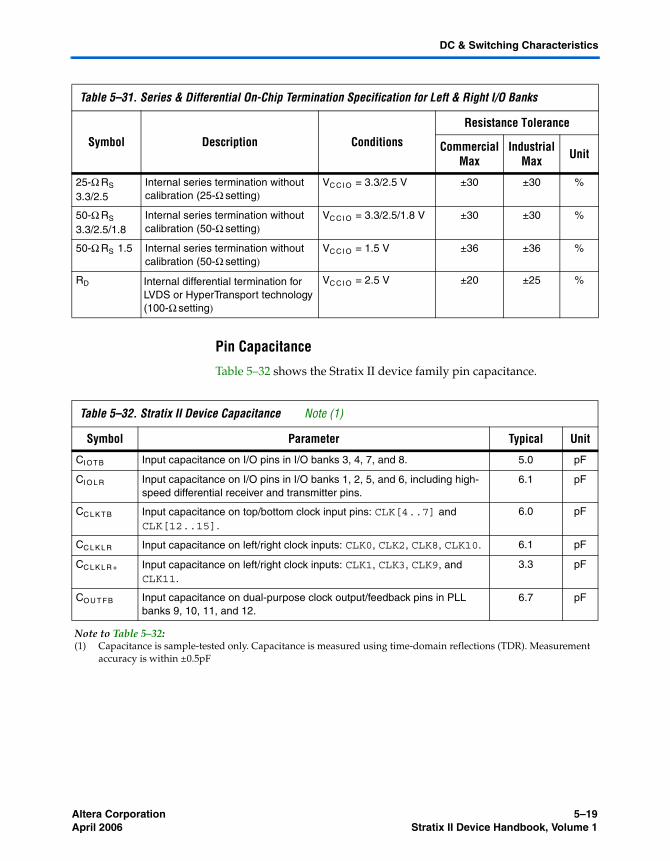
Altera Corporation 5–19April 2006 Stratix II Device Handbook, Volume 1
DC & Switching Characteristics
Pin Capacitance
Table 5–32 shows the Stratix II device family pin capacitance.
Table 5–31. Series & Differential On-Chip Termination Specification for Left & Right I/O Banks
Symbol Description Conditions
Resistance Tolerance
Commercial Max
Industrial Max Unit
25-Ω RS 3.3/2.5
Internal series termination without calibration (25-Ω setting)
VC CI O = 3.3/2.5 V ±30 ±30 %
50-Ω RS 3.3/2.5/1.8
Internal series termination without calibration (50-Ω setting)
VC CI O = 3.3/2.5/1.8 V ±30 ±30 %
50-Ω RS 1.5 Internal series termination without calibration (50-Ω setting)
VC CI O = 1.5 V ±36 ±36 %
RD Internal differential termination for LVDS or HyperTransport technology (100-Ω setting)
VC CI O = 2.5 V ±20 ±25 %
Table 5–32. Stratix II Device Capacitance Note (1)
Symbol Parameter Typical Unit
CI OT B Input capacitance on I/O pins in I/O banks 3, 4, 7, and 8. 5.0 pF
CI O L R Input capacitance on I/O pins in I/O banks 1, 2, 5, and 6, including high-speed differential receiver and transmitter pins.
6.1 pF
CC L K T B Input capacitance on top/bottom clock input pins: CLK[4..7] and CLK[12..15].
6.0 pF
CC L K L R Input capacitance on left/right clock inputs: CLK0, CLK2, CLK8, CLK10. 6.1 pF
CC L K L R + Input capacitance on left/right clock inputs: CLK1, CLK3, CLK9, and CLK11.
3.3 pF
CO U T F B Input capacitance on dual-purpose clock output/feedback pins in PLL banks 9, 10, 11, and 12.
6.7 pF
Note to Table 5–32:(1) Capacitance is sample-tested only. Capacitance is measured using time-domain reflections (TDR). Measurement
accuracy is within ±0.5pF
5–20 Altera CorporationStratix II Device Handbook, Volume 1 April 2006
Power Consumption
Power Consumption
Altera® offers two ways to calculate power for a design: the Excel-based PowerPlay Early Power Estimator power calculator and the Quartus® II PowerPlay Power Analyzer feature.
The interactive Excel-based PowerPlay Early Power Estimator is typically used prior to designing the FPGA in order to get an estimate of device power. The Quartus II PowerPlay Power Analyzer provides better quality estimates based on the specifics of the design after place-and-route is complete. The Power Analyzer can apply a combination of user-entered, simulation-derived and estimated signal activities which, combined with detailed circuit models, can yield very accurate power estimates.
In both cases, these calculations should only be used as an estimation of power, not as a specification.
f For more information on PowerPlay tools, refer to the PowerPlay Early Power Estimator User Guide and the PowerPlay Early Power Estimator and PowerPlay Power Analyzer chapters in Volume 3 of the Quartus II Handbook.
The PowerPlay Early Power Estimator is available on the Altera web site at www.altera. com. See Table 5–4 on page 5–3 for typical ICC standby specifications.
Timing Model The DirectDriveTM technology and MultiTrackTM interconnect ensure predictable performance, accurate simulation, and accurate timing analysis across all Stratix II device densities and speed grades. This section describes and specifies the performance, internal timing, external timing, and PLL, high-speed I/O, external memory interface, and JTAG timing specifications.
All specifications are representative of worst-case supply voltage and junction temperature conditions.
1 The timing numbers listed in the tables of this section are extracted from the Quartus II software version 5.0 SP1.
Preliminary & Final Timing
Timing models can have either preliminary or final status. The Quartus II software issues an informational message during the design compilation if the timing models are preliminary. Table 5–33 shows the status of the Stratix II device timing models.
Altera Corporation 5–21April 2006 Stratix II Device Handbook, Volume 1
DC & Switching Characteristics
Preliminary status means the timing model is subject to change. Initially, timing numbers are created using simulation results, process data, and other known parameters. These tests are used to make the preliminary numbers as close to the actual timing parameters as possible.
Final timing numbers are based on actual device operation and testing. These numbers reflect the actual performance of the device under worst-case voltage and junction temperature conditions.
I/O Timing Measurement Methodology
Altera characterizes timing delays at the worst-case process, minimum voltage, and maximum temperature for input register setup time (tSU) and hold time (tH). The Quartus II software uses the following equations to calculate tSU and tH timing for Stratix II devices input signals.
tSU = + data delay from input pin to input register+ micro setup time of the input register– clock delay from input pin to input register
tH = – data delay from input pin to input register+ micro hold time of the input register+ clock delay from input pin to input register
Figure 5–3 shows the setup and hold timing diagram for input registers.
Table 5–33. Stratix II Device Timing Model Status
Device Preliminary Final
EP2S15 v
EP2S30 v
EP2S60 v
EP2S90 v
EP2S130 v
EP2S180 v
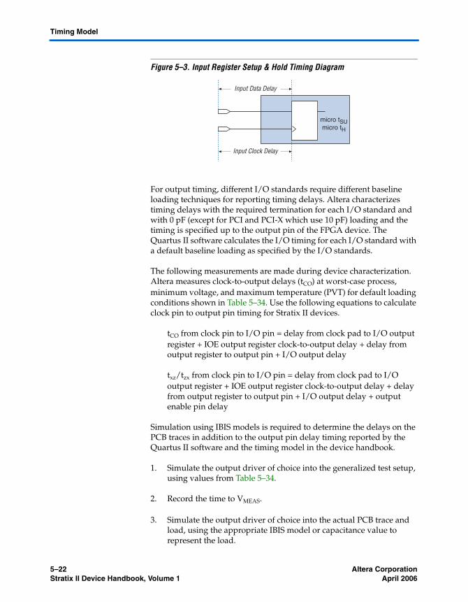
5–22 Altera CorporationStratix II Device Handbook, Volume 1 April 2006
Timing Model
Figure 5–3. Input Register Setup & Hold Timing Diagram
For output timing, different I/O standards require different baseline loading techniques for reporting timing delays. Altera characterizes timing delays with the required termination for each I/O standard and with 0 pF (except for PCI and PCI-X which use 10 pF) loading and the timing is specified up to the output pin of the FPGA device. The Quartus II software calculates the I/O timing for each I/O standard with a default baseline loading as specified by the I/O standards.
The following measurements are made during device characterization. Altera measures clock-to-output delays (tCO) at worst-case process, minimum voltage, and maximum temperature (PVT) for default loading conditions shown in Table 5–34. Use the following equations to calculate clock pin to output pin timing for Stratix II devices.
tCO from clock pin to I/O pin = delay from clock pad to I/O output register + IOE output register clock-to-output delay + delay from output register to output pin + I/O output delay
txz/tzx from clock pin to I/O pin = delay from clock pad to I/O output register + IOE output register clock-to-output delay + delay from output register to output pin + I/O output delay + output enable pin delay
Simulation using IBIS models is required to determine the delays on the PCB traces in addition to the output pin delay timing reported by the Quartus II software and the timing model in the device handbook.
1. Simulate the output driver of choice into the generalized test setup, using values from Table 5–34.
2. Record the time to VMEAS.
3. Simulate the output driver of choice into the actual PCB trace and load, using the appropriate IBIS model or capacitance value to represent the load.
Input Data Delay
Input Clock Delay
micro tSUmicro tH
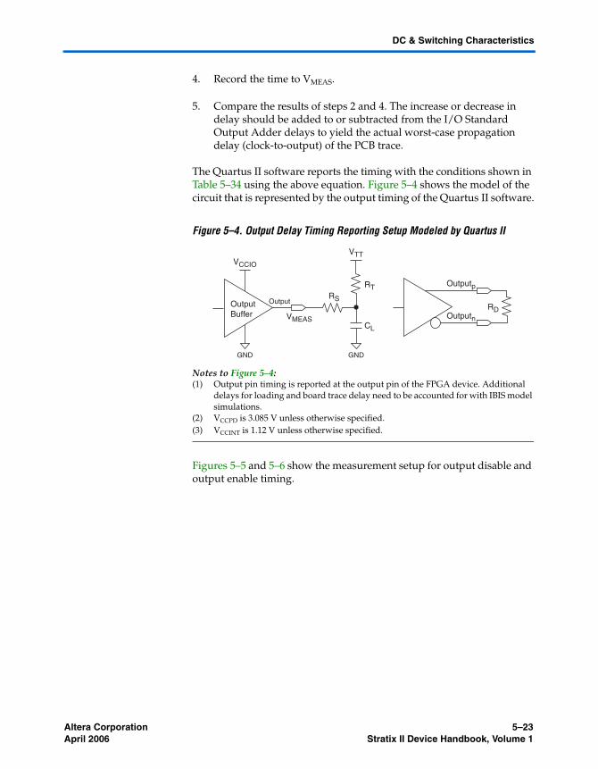
Altera Corporation 5–23April 2006 Stratix II Device Handbook, Volume 1
DC & Switching Characteristics
4. Record the time to VMEAS.
5. Compare the results of steps 2 and 4. The increase or decrease in delay should be added to or subtracted from the I/O Standard Output Adder delays to yield the actual worst-case propagation delay (clock-to-output) of the PCB trace.
The Quartus II software reports the timing with the conditions shown in Table 5–34 using the above equation. Figure 5–4 shows the model of the circuit that is represented by the output timing of the Quartus II software.
Figure 5–4. Output Delay Timing Reporting Setup Modeled by Quartus II
Notes to Figure 5–4:(1) Output pin timing is reported at the output pin of the FPGA device. Additional
delays for loading and board trace delay need to be accounted for with IBIS model simulations.
(2) VCCPD is 3.085 V unless otherwise specified.(3) VCCINT is 1.12 V unless otherwise specified.
Figures 5–5 and 5–6 show the measurement setup for output disable and output enable timing.
OutputBuffer
VTTVCCIO
RDOutputn
OutputpRT
CL
RS
VMEAS
Output
GND GND
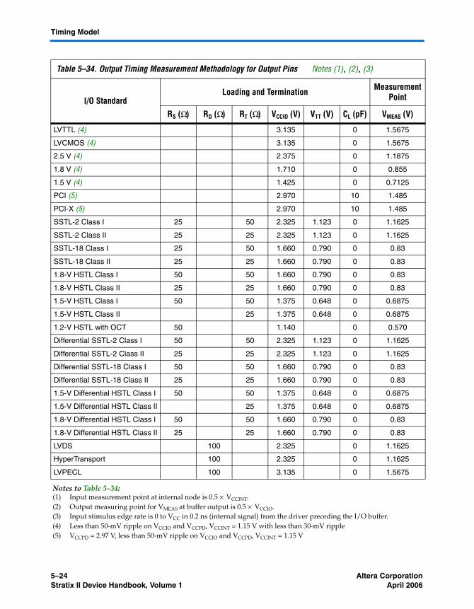
5–24 Altera CorporationStratix II Device Handbook, Volume 1 April 2006
Timing Model
Table 5–34. Output Timing Measurement Methodology for Output Pins Notes (1), (2), (3)
I/O StandardLoading and Termination Measurement
Point
RS (Ω) RD (Ω) RT (Ω) VCCIO (V) VTT (V) CL (pF) VMEAS (V)
LVTTL (4) 3.135 0 1.5675
LVCMOS (4) 3.135 0 1.5675
2.5 V (4) 2.375 0 1.1875
1.8 V (4) 1.710 0 0.855
1.5 V (4) 1.425 0 0.7125
PCI (5) 2.970 10 1.485
PCI-X (5) 2.970 10 1.485
SSTL-2 Class I 25 50 2.325 1.123 0 1.1625
SSTL-2 Class II 25 25 2.325 1.123 0 1.1625
SSTL-18 Class I 25 50 1.660 0.790 0 0.83
SSTL-18 Class II 25 25 1.660 0.790 0 0.83
1.8-V HSTL Class I 50 50 1.660 0.790 0 0.83
1.8-V HSTL Class II 25 25 1.660 0.790 0 0.83
1.5-V HSTL Class I 50 50 1.375 0.648 0 0.6875
1.5-V HSTL Class II 25 1.375 0.648 0 0.6875
1.2-V HSTL with OCT 50 1.140 0 0.570
Differential SSTL-2 Class I 50 50 2.325 1.123 0 1.1625
Differential SSTL-2 Class II 25 25 2.325 1.123 0 1.1625
Differential SSTL-18 Class I 50 50 1.660 0.790 0 0.83
Differential SSTL-18 Class II 25 25 1.660 0.790 0 0.83
1.5-V Differential HSTL Class I 50 50 1.375 0.648 0 0.6875
1.5-V Differential HSTL Class II 25 1.375 0.648 0 0.6875
1.8-V Differential HSTL Class I 50 50 1.660 0.790 0 0.83
1.8-V Differential HSTL Class II 25 25 1.660 0.790 0 0.83
LVDS 100 2.325 0 1.1625
HyperTransport 100 2.325 0 1.1625
LVPECL 100 3.135 0 1.5675
Notes to Table 5–34:(1) Input measurement point at internal node is 0.5 × VCCINT.(2) Output measuring point for VMEAS at buffer output is 0.5 × VCCIO.(3) Input stimulus edge rate is 0 to VCC in 0.2 ns (internal signal) from the driver preceding the I/O buffer.(4) Less than 50-mV ripple on VCCIO and VCCPD, VCCINT = 1.15 V with less than 30-mV ripple(5) VCCPD = 2.97 V, less than 50-mV ripple on VCCIO and VCCPD, VCCINT = 1.15 V
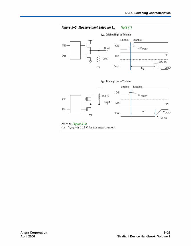
Altera Corporation 5–25April 2006 Stratix II Device Handbook, Volume 1
DC & Switching Characteristics
Figure 5–5. Measurement Setup for txz Note (1)
Note to Figure 5–5:(1) VCCINT is 1.12 V for this measurement.
tXZ, Driving High to Tristate
tXZ, Driving Low to Tristate
100 Ω
Din
OEDout
VCCIO
OE
Enable Disable
Dout
Din
tlz
100 mv
½ VCCINT
“0”
100 ΩDin
OEDout
OE
Enable Disable
Dout
Din
thz
100 mv
½ VCCINT
“1”
GND
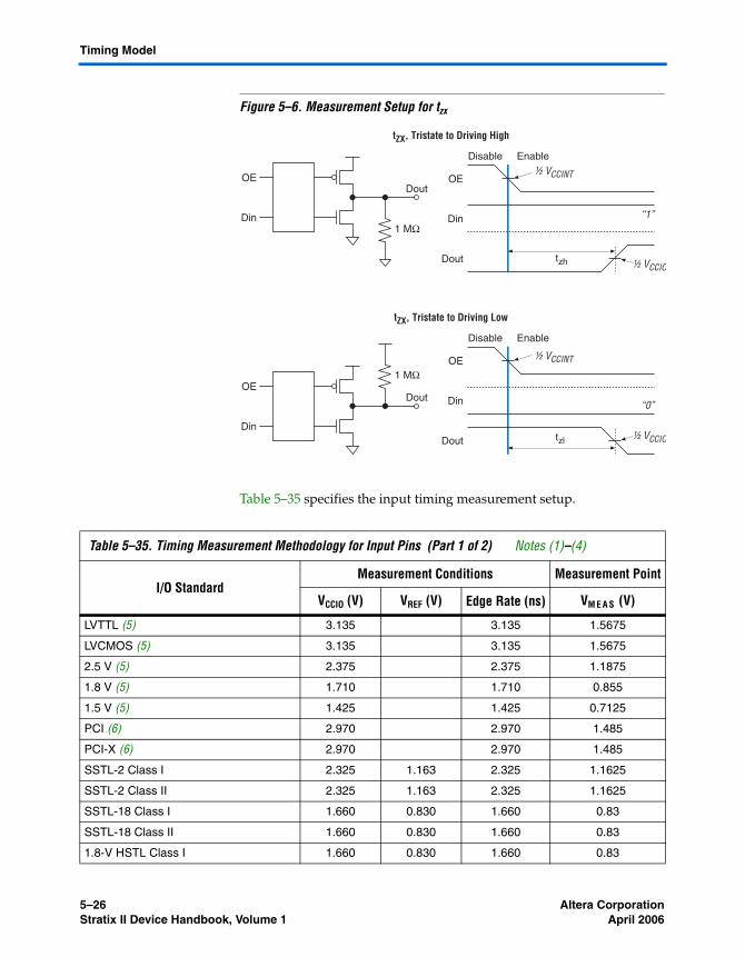
5–26 Altera CorporationStratix II Device Handbook, Volume 1 April 2006
Timing Model
Figure 5–6. Measurement Setup for tzx
Table 5–35 specifies the input timing measurement setup.
tZX, Tristate to Driving High
tZX, Tristate to Driving Low
1 MΩ
Din
OEDout
1 MΩDin
OEDout
OE
Disable Enable
Dout
Din
tzh
½ VCCINT
“1”
½ VCCIO
OE
Disable Enable
Dout
Din
½ VCCINT
“0”
tzl ½ VCCIO
Table 5–35. Timing Measurement Methodology for Input Pins (Part 1 of 2) Notes (1)–(4)
I/O StandardMeasurement Conditions Measurement Point
VCCIO (V) VREF (V) Edge Rate (ns) VM E A S (V)
LVTTL (5) 3.135 3.135 1.5675
LVCMOS (5) 3.135 3.135 1.5675
2.5 V (5) 2.375 2.375 1.1875
1.8 V (5) 1.710 1.710 0.855
1.5 V (5) 1.425 1.425 0.7125
PCI (6) 2.970 2.970 1.485
PCI-X (6) 2.970 2.970 1.485
SSTL-2 Class I 2.325 1.163 2.325 1.1625
SSTL-2 Class II 2.325 1.163 2.325 1.1625
SSTL-18 Class I 1.660 0.830 1.660 0.83
SSTL-18 Class II 1.660 0.830 1.660 0.83
1.8-V HSTL Class I 1.660 0.830 1.660 0.83
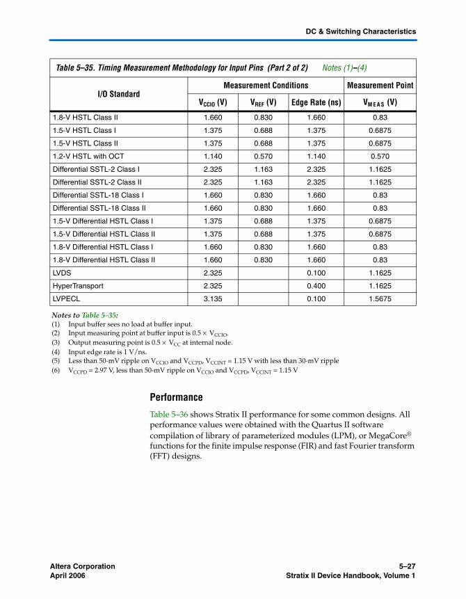
Altera Corporation 5–27April 2006 Stratix II Device Handbook, Volume 1
DC & Switching Characteristics
Performance
Table 5–36 shows Stratix II performance for some common designs. All performance values were obtained with the Quartus II software compilation of library of parameterized modules (LPM), or MegaCore® functions for the finite impulse response (FIR) and fast Fourier transform (FFT) designs.
1.8-V HSTL Class II 1.660 0.830 1.660 0.83
1.5-V HSTL Class I 1.375 0.688 1.375 0.6875
1.5-V HSTL Class II 1.375 0.688 1.375 0.6875
1.2-V HSTL with OCT 1.140 0.570 1.140 0.570
Differential SSTL-2 Class I 2.325 1.163 2.325 1.1625
Differential SSTL-2 Class II 2.325 1.163 2.325 1.1625
Differential SSTL-18 Class I 1.660 0.830 1.660 0.83
Differential SSTL-18 Class II 1.660 0.830 1.660 0.83
1.5-V Differential HSTL Class I 1.375 0.688 1.375 0.6875
1.5-V Differential HSTL Class II 1.375 0.688 1.375 0.6875
1.8-V Differential HSTL Class I 1.660 0.830 1.660 0.83
1.8-V Differential HSTL Class II 1.660 0.830 1.660 0.83
LVDS 2.325 0.100 1.1625
HyperTransport 2.325 0.400 1.1625
LVPECL 3.135 0.100 1.5675
Notes to Table 5–35:(1) Input buffer sees no load at buffer input.(2) Input measuring point at buffer input is 0.5 × VCCIO.(3) Output measuring point is 0.5 × VCC at internal node.(4) Input edge rate is 1 V/ns.(5) Less than 50-mV ripple on VCCIO and VCCPD, VCCINT = 1.15 V with less than 30-mV ripple(6) VCCPD = 2.97 V, less than 50-mV ripple on VCCIO and VCCPD, VCCINT = 1.15 V
Table 5–35. Timing Measurement Methodology for Input Pins (Part 2 of 2) Notes (1)–(4)
I/O StandardMeasurement Conditions Measurement Point
VCCIO (V) VREF (V) Edge Rate (ns) VM E A S (V)
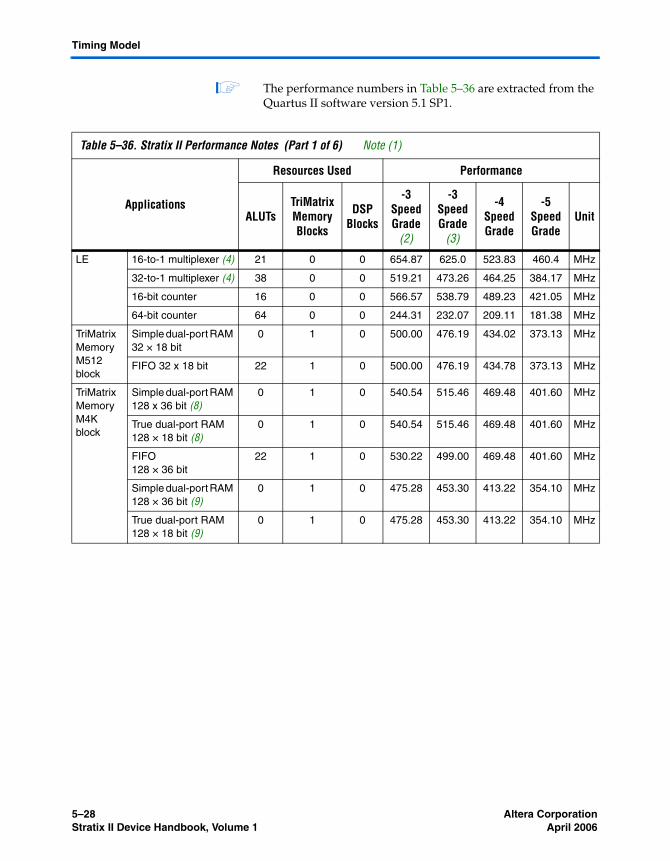
5–28 Altera CorporationStratix II Device Handbook, Volume 1 April 2006
Timing Model
1 The performance numbers in Table 5–36 are extracted from the Quartus II software version 5.1 SP1.
Table 5–36. Stratix II Performance Notes (Part 1 of 6) Note (1)
Applications
Resources Used Performance
ALUTsTriMatrix Memory Blocks
DSP Blocks
-3 Speed Grade
(2)
-3 Speed Grade
(3)
-4 Speed Grade
-5 Speed Grade
Unit
LE 16-to-1 multiplexer (4) 21 0 0 654.87 625.0 523.83 460.4 MHz
32-to-1 multiplexer (4) 38 0 0 519.21 473.26 464.25 384.17 MHz
16-bit counter 16 0 0 566.57 538.79 489.23 421.05 MHz
64-bit counter 64 0 0 244.31 232.07 209.11 181.38 MHz
TriMatrix Memory M512 block
Simple dual-port RAM 32 × 18 bit
0 1 0 500.00 476.19 434.02 373.13 MHz
FIFO 32 x 18 bit 22 1 0 500.00 476.19 434.78 373.13 MHz
TriMatrix Memory M4K block
Simple dual-port RAM 128 x 36 bit (8)
0 1 0 540.54 515.46 469.48 401.60 MHz
True dual-port RAM 128 × 18 bit (8)
0 1 0 540.54 515.46 469.48 401.60 MHz
FIFO 128 × 36 bit
22 1 0 530.22 499.00 469.48 401.60 MHz
Simple dual-port RAM 128 × 36 bit (9)
0 1 0 475.28 453.30 413.22 354.10 MHz
True dual-port RAM 128 × 18 bit (9)
0 1 0 475.28 453.30 413.22 354.10 MHz
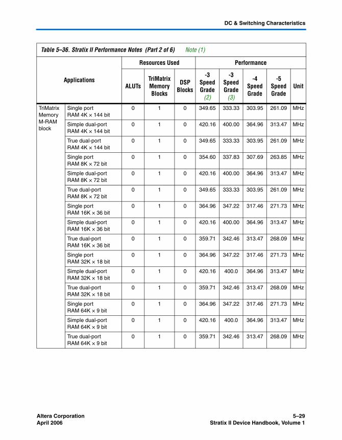
Altera Corporation 5–29April 2006 Stratix II Device Handbook, Volume 1
DC & Switching Characteristics
TriMatrix Memory M-RAM block
Single port RAM 4K × 144 bit
0 1 0 349.65 333.33 303.95 261.09 MHz
Simple dual-port RAM 4K × 144 bit
0 1 0 420.16 400.00 364.96 313.47 MHz
True dual-port RAM 4K × 144 bit
0 1 0 349.65 333.33 303.95 261.09 MHz
Single port RAM 8K × 72 bit
0 1 0 354.60 337.83 307.69 263.85 MHz
Simple dual-port RAM 8K × 72 bit
0 1 0 420.16 400.00 364.96 313.47 MHz
True dual-portRAM 8K × 72 bit
0 1 0 349.65 333.33 303.95 261.09 MHz
Single portRAM 16K × 36 bit
0 1 0 364.96 347.22 317.46 271.73 MHz
Simple dual-portRAM 16K × 36 bit
0 1 0 420.16 400.00 364.96 313.47 MHz
True dual-port RAM 16K × 36 bit
0 1 0 359.71 342.46 313.47 268.09 MHz
Single portRAM 32K × 18 bit
0 1 0 364.96 347.22 317.46 271.73 MHz
Simple dual-port RAM 32K × 18 bit
0 1 0 420.16 400.0 364.96 313.47 MHz
True dual-port RAM 32K × 18 bit
0 1 0 359.71 342.46 313.47 268.09 MHz
Single port RAM 64K × 9 bit
0 1 0 364.96 347.22 317.46 271.73 MHz
Simple dual-port RAM 64K × 9 bit
0 1 0 420.16 400.0 364.96 313.47 MHz
True dual-port RAM 64K × 9 bit
0 1 0 359.71 342.46 313.47 268.09 MHz
Table 5–36. Stratix II Performance Notes (Part 2 of 6) Note (1)
Applications
Resources Used Performance
ALUTsTriMatrix Memory Blocks
DSP Blocks
-3 Speed Grade
(2)
-3 Speed Grade
(3)
-4 Speed Grade
-5 Speed Grade
Unit
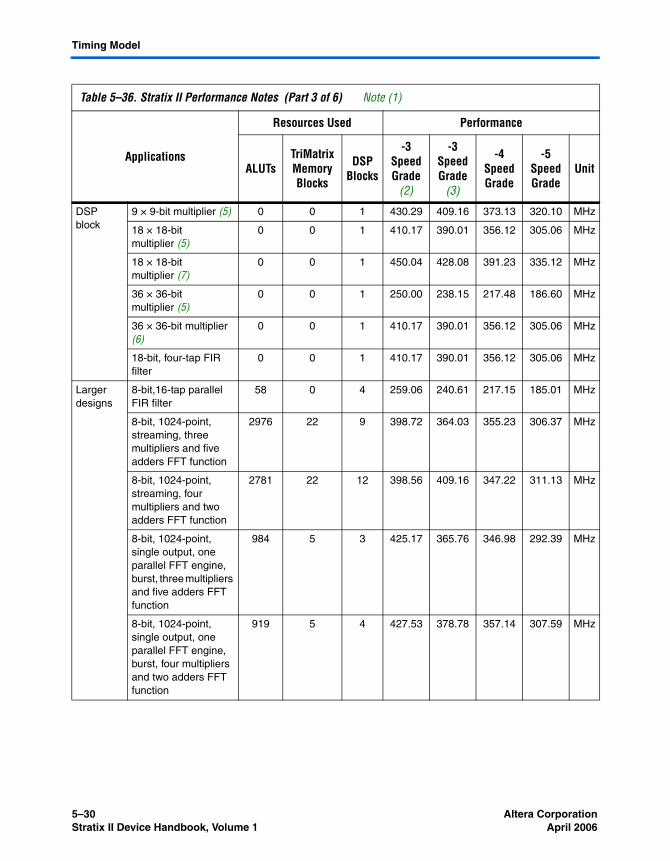
5–30 Altera CorporationStratix II Device Handbook, Volume 1 April 2006
Timing Model
DSP block
9 × 9-bit multiplier (5) 0 0 1 430.29 409.16 373.13 320.10 MHz
18 × 18-bit multiplier (5)
0 0 1 410.17 390.01 356.12 305.06 MHz
18 × 18-bit multiplier (7)
0 0 1 450.04 428.08 391.23 335.12 MHz
36 × 36-bit multiplier (5)
0 0 1 250.00 238.15 217.48 186.60 MHz
36 × 36-bit multiplier (6)
0 0 1 410.17 390.01 356.12 305.06 MHz
18-bit, four-tap FIR filter
0 0 1 410.17 390.01 356.12 305.06 MHz
Larger designs
8-bit,16-tap parallel FIR filter
58 0 4 259.06 240.61 217.15 185.01 MHz
8-bit, 1024-point, streaming, three multipliers and five adders FFT function
2976 22 9 398.72 364.03 355.23 306.37 MHz
8-bit, 1024-point, streaming, four multipliers and two adders FFT function
2781 22 12 398.56 409.16 347.22 311.13 MHz
8-bit, 1024-point, single output, one parallel FFT engine, burst, three multipliers and five adders FFT function
984 5 3 425.17 365.76 346.98 292.39 MHz
8-bit, 1024-point, single output, one parallel FFT engine, burst, four multipliers and two adders FFT function
919 5 4 427.53 378.78 357.14 307.59 MHz
Table 5–36. Stratix II Performance Notes (Part 3 of 6) Note (1)
Applications
Resources Used Performance
ALUTsTriMatrix Memory Blocks
DSP Blocks
-3 Speed Grade
(2)
-3 Speed Grade
(3)
-4 Speed Grade
-5 Speed Grade
Unit
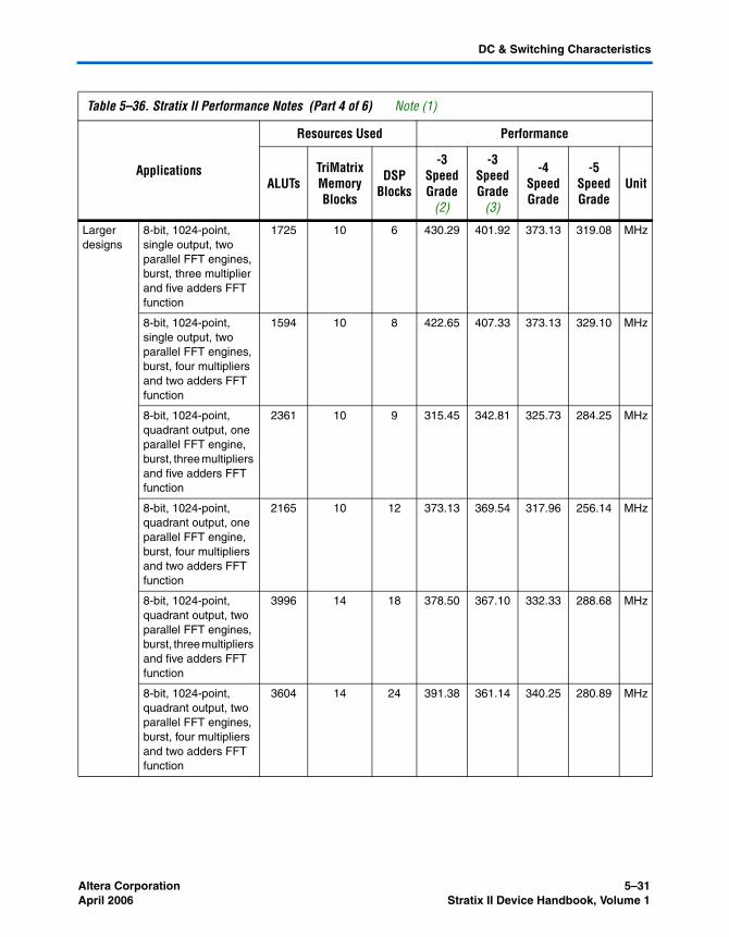
Altera Corporation 5–31April 2006 Stratix II Device Handbook, Volume 1
DC & Switching Characteristics
Larger designs
8-bit, 1024-point, single output, two parallel FFT engines, burst, three multiplier and five adders FFT function
1725 10 6 430.29 401.92 373.13 319.08 MHz
8-bit, 1024-point, single output, two parallel FFT engines, burst, four multipliers and two adders FFT function
1594 10 8 422.65 407.33 373.13 329.10 MHz
8-bit, 1024-point, quadrant output, one parallel FFT engine, burst, three multipliers and five adders FFT function
2361 10 9 315.45 342.81 325.73 284.25 MHz
8-bit, 1024-point, quadrant output, one parallel FFT engine, burst, four multipliers and two adders FFT function
2165 10 12 373.13 369.54 317.96 256.14 MHz
8-bit, 1024-point, quadrant output, two parallel FFT engines, burst, three multipliers and five adders FFT function
3996 14 18 378.50 367.10 332.33 288.68 MHz
8-bit, 1024-point, quadrant output, two parallel FFT engines, burst, four multipliers and two adders FFT function
3604 14 24 391.38 361.14 340.25 280.89 MHz
Table 5–36. Stratix II Performance Notes (Part 4 of 6) Note (1)
Applications
Resources Used Performance
ALUTsTriMatrix Memory Blocks
DSP Blocks
-3 Speed Grade
(2)
-3 Speed Grade
(3)
-4 Speed Grade
-5 Speed Grade
Unit
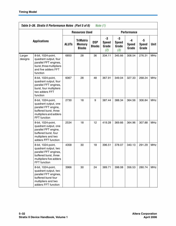
5–32 Altera CorporationStratix II Device Handbook, Volume 1 April 2006
Timing Model
Larger designs
8-bit, 1024-point, quadrant output, four parallel FFT engines, burst, three multipliers and five adders FFT function
6850 28 36 334.11 345.66 308.54 276.31 MHz
8-bit, 1024-point, quadrant output, four parallel FFT engines, burst, four multipliers two adders FFT function
6067 28 48 367.91 349.04 327.33 268.24 MHz
8-bit, 1024-point, quadrant output, one parallel FFT engine, buffered burst, three multipliers and adders FFT function
2730 18 9 387.44 388.34 364.56 306.84 MHz
8-bit, 1024-point, quadrant output, one parallel FFT engine, buffered burst, four multipliers and two adders FFT function
2534 18 12 419.28 369.66 364.96 307.88 MHz
8-bit, 1024-point, quadrant output, two parallel FFT engines, buffered burst, three multipliers five adders FFT function
4358 30 18 396.51 378.07 340.13 291.29 MHz
8-bit, 1024-point, quadrant output, two parallel FFT engines, buffered burst four multipliers and two adders FFT function
3966 30 24 389.71 398.08 356.53 280.74 MHz
Table 5–36. Stratix II Performance Notes (Part 5 of 6) Note (1)
Applications
Resources Used Performance
ALUTsTriMatrix Memory Blocks
DSP Blocks
-3 Speed Grade
(2)
-3 Speed Grade
(3)
-4 Speed Grade
-5 Speed Grade
Unit
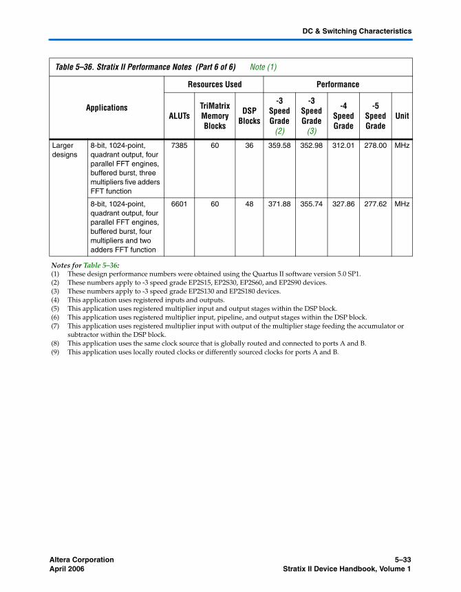
Altera Corporation 5–33April 2006 Stratix II Device Handbook, Volume 1
DC & Switching Characteristics
Larger designs
8-bit, 1024-point, quadrant output, four parallel FFT engines, buffered burst, three multipliers five adders FFT function
7385 60 36 359.58 352.98 312.01 278.00 MHz
8-bit, 1024-point, quadrant output, four parallel FFT engines, buffered burst, four multipliers and two adders FFT function
6601 60 48 371.88 355.74 327.86 277.62 MHz
Notes for Table 5–36:(1) These design performance numbers were obtained using the Quartus II software version 5.0 SP1.(2) These numbers apply to -3 speed grade EP2S15, EP2S30, EP2S60, and EP2S90 devices.(3) These numbers apply to -3 speed grade EP2S130 and EP2S180 devices.(4) This application uses registered inputs and outputs.(5) This application uses registered multiplier input and output stages within the DSP block.(6) This application uses registered multiplier input, pipeline, and output stages within the DSP block.(7) This application uses registered multiplier input with output of the multiplier stage feeding the accumulator or
subtractor within the DSP block.(8) This application uses the same clock source that is globally routed and connected to ports A and B.(9) This application uses locally routed clocks or differently sourced clocks for ports A and B.
Table 5–36. Stratix II Performance Notes (Part 6 of 6) Note (1)
Applications
Resources Used Performance
ALUTsTriMatrix Memory Blocks
DSP Blocks
-3 Speed Grade
(2)
-3 Speed Grade
(3)
-4 Speed Grade
-5 Speed Grade
Unit
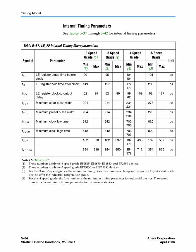
5–34 Altera CorporationStratix II Device Handbook, Volume 1 April 2006
Timing Model
Internal Timing Parameters
See Tables 5–37 through 5–42 for internal timing parameters.
Table 5–37. LE_FF Internal Timing Microparameters
Symbol Parameter
-3 Speed Grade (1)
-3 Speed Grade (2)
-4 Speed Grade
-5 Speed Grade
UnitMin (3) Max Min
(3) Max Min (4) Max Min
(3) Max
tS U LE register setup time before clock
90 95 104104
121 ps
tH LE register hold time after clock 149 157 172172
200 ps
tC O LE register clock-to-output delay
62 94 62 99 5962
109 62 127 ps
tC L R Minimum clear pulse width 204 214 234234
273 ps
tP R E Minimum preset pulse width 204 214 234234
273 ps
tC L K L Minimum clock low time 612 642 703703
820 ps
tC L K H Minimum clock high time 612 642 703703
820 ps
tL U T 162 378 162 397 162170
435 162 507 ps
tA D D E R 354 619 354 650 354372
712 354 829 ps
Notes to Table 5–37:(1) These numbers apply to -3 speed grade EP2S15, EP2S30, EP2S60, and EP2S90 devices.(2) These numbers apply to -3 speed grade EP2S130 and EP2S180 devices.(3) For the -3 and -5 speed grades, the minimum timing is for the commercial temperature grade. Only -4 speed grade
devices offer the industrial temperature grade.(4) For the -4 speed grade, the first number is the minimum timing parameter for industrial devices. The second
number is the minimum timing parameter for commercial devices.
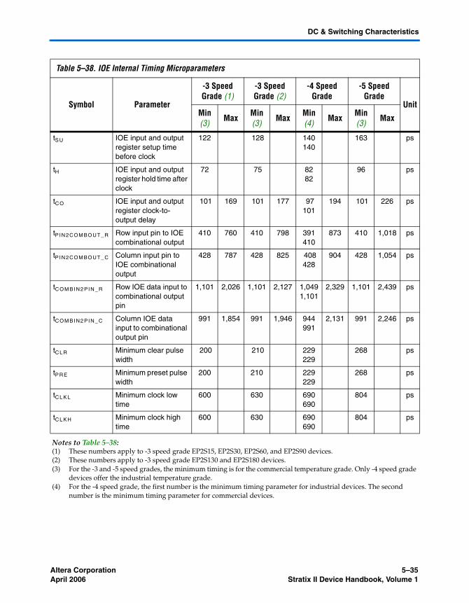
Altera Corporation 5–35April 2006 Stratix II Device Handbook, Volume 1
DC & Switching Characteristics
Table 5–38. IOE Internal Timing Microparameters
Symbol Parameter
-3 Speed Grade (1)
-3 Speed Grade (2)
-4 Speed Grade
-5 Speed Grade
UnitMin (3) Max Min
(3) Max Min (4) Max Min
(3) Max
tS U IOE input and output register setup time before clock
122 128 140140
163 ps
tH IOE input and output register hold time after clock
72 75 8282
96 ps
tC O IOE input and output register clock-to-output delay
101 169 101 177 97101
194 101 226 ps
tP IN 2C O M BO UT _R Row input pin to IOE combinational output
410 760 410 798 391410
873 410 1,018 ps
tP IN 2C O M BO UT _C Column input pin to IOE combinational output
428 787 428 825 408428
904 428 1,054 ps
tC O M B I N2 P I N _ R Row IOE data input to combinational output pin
1,101 2,026 1,101 2,127 1,0491,101
2,329 1,101 2,439 ps
tC O M B I N2 P I N _ C Column IOE data input to combinational output pin
991 1,854 991 1,946 944991
2,131 991 2,246 ps
tC L R Minimum clear pulse width
200 210 229229
268 ps
tP R E Minimum preset pulse width
200 210 229229
268 ps
tC L K L Minimum clock low time
600 630 690690
804 ps
tC L K H Minimum clock high time
600 630 690690
804 ps
Notes to Table 5–38:(1) These numbers apply to -3 speed grade EP2S15, EP2S30, EP2S60, and EP2S90 devices.(2) These numbers apply to -3 speed grade EP2S130 and EP2S180 devices.(3) For the -3 and -5 speed grades, the minimum timing is for the commercial temperature grade. Only -4 speed grade
devices offer the industrial temperature grade.(4) For the -4 speed grade, the first number is the minimum timing parameter for industrial devices. The second
number is the minimum timing parameter for commercial devices.
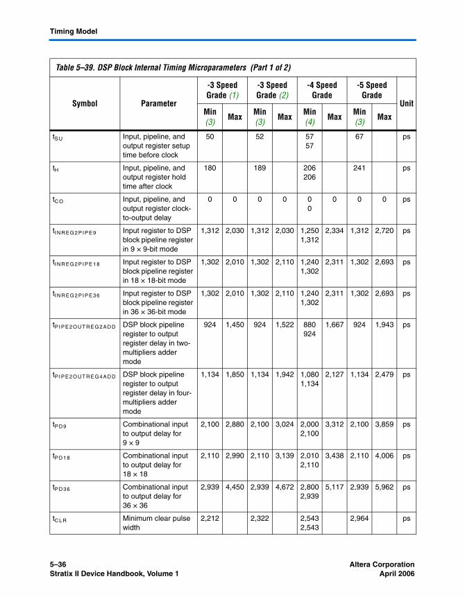
5–36 Altera CorporationStratix II Device Handbook, Volume 1 April 2006
Timing Model
Table 5–39. DSP Block Internal Timing Microparameters (Part 1 of 2)
Symbol Parameter
-3 Speed Grade (1)
-3 Speed Grade (2)
-4 Speed Grade
-5 Speed Grade
UnitMin (3) Max Min
(3) Max Min (4) Max Min
(3) Max
tS U Input, pipeline, and output register setup time before clock
50 52 5757
67 ps
tH Input, pipeline, and output register hold time after clock
180 189 206206
241 ps
tC O Input, pipeline, and output register clock-to-output delay
0 0 0 0 00
0 0 0 ps
tI N R E G 2 P I P E 9 Input register to DSP block pipeline register in 9 × 9-bit mode
1,312 2,030 1,312 2,030 1,2501,312
2,334 1,312 2,720 ps
tI N R E G 2 P I P E 1 8 Input register to DSP block pipeline register in 18 × 18-bit mode
1,302 2,010 1,302 2,110 1,2401,302
2,311 1,302 2,693 ps
tI N R E G 2 P I P E 3 6 Input register to DSP block pipeline register in 36 × 36-bit mode
1,302 2,010 1,302 2,110 1,2401,302
2,311 1,302 2,693 ps
tP I P E 2 O U T R E G 2 A D D DSP block pipeline register to output register delay in two-multipliers adder mode
924 1,450 924 1,522 880924
1,667 924 1,943 ps
tP I P E 2 O U T R E G 4 A D D DSP block pipeline register to output register delay in four-multipliers adder mode
1,134 1,850 1,134 1,942 1,0801,134
2,127 1,134 2,479 ps
tP D 9 Combinational input to output delay for 9 × 9
2,100 2,880 2,100 3,024 2,0002,100
3,312 2,100 3,859 ps
tP D 1 8 Combinational input to output delay for 18 × 18
2,110 2,990 2,110 3,139 2,0102,110
3,438 2,110 4,006 ps
tP D 3 6 Combinational input to output delay for 36 × 36
2,939 4,450 2,939 4,672 2,8002,939
5,117 2,939 5,962 ps
tC L R Minimum clear pulse width
2,212 2,322 2,5432,543
2,964 ps
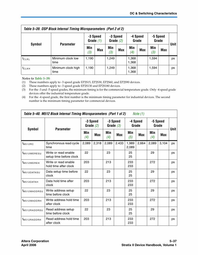
Altera Corporation 5–37April 2006 Stratix II Device Handbook, Volume 1
DC & Switching Characteristics
tC L K L Minimum clock low time
1,190 1,249 1,3681,368
1,594 ps
tC L K H Minimum clock high time
1,190 1,249 1,3681,368
1,594 ps
Notes to Table 5–39:(1) These numbers apply to -3 speed grade EP2S15, EP2S30, EP2S60, and EP2S90 devices.(2) These numbers apply to -3 speed grade EP2S130 and EP2S180 devices.(3) For the -3 and -5 speed grades, the minimum timing is for the commercial temperature grade. Only -4 speed grade
devices offer the industrial temperature grade.(4) For the -4 speed grade, the first number is the minimum timing parameter for industrial devices. The second
number is the minimum timing parameter for commercial devices.
Table 5–40. M512 Block Internal Timing Microparameters (Part 1 of 2) Note (1)
Symbol Parameter
-3 Speed Grade (2)
-3 Speed Grade (3)
-4 Speed Grade
-5 Speed Grade
UnitMin (4) Max Min
(4) Max Min (5) Max Min
(4) Max
tM 5 1 2 R C Synchronous read cycle time
2,089 2,318 2,089 2.433 1,9892,089
2,664 2,089 3,104 ps
tM 5 1 2 W E R E S U Write or read enable setup time before clock
22 23 2525
29 ps
tM 5 1 2 W E R E H Write or read enable hold time after clock
203 213 233233
272 ps
tM 5 1 2 DATA S U Data setup time before clock
22 23 2525
29 ps
tM 5 1 2 DATA H Data hold time after clock
203 213 233233
272 ps
tM512 WA DDRSU Write address setup time before clock
22 23 2525
29 ps
tM 5 1 2 WA D D RH Write address hold time after clock
203 213 233233
272 ps
tM 5 1 2 RA D DR S U Read address setup time before clock
22 23 2525
29 ps
tM 5 1 2 RA D DR H Read address hold time after clock
203 213 233233
272 ps
Table 5–39. DSP Block Internal Timing Microparameters (Part 2 of 2)
Symbol Parameter
-3 Speed Grade (1)
-3 Speed Grade (2)
-4 Speed Grade
-5 Speed Grade
UnitMin (3) Max Min
(3) Max Min (4) Max Min
(3) Max
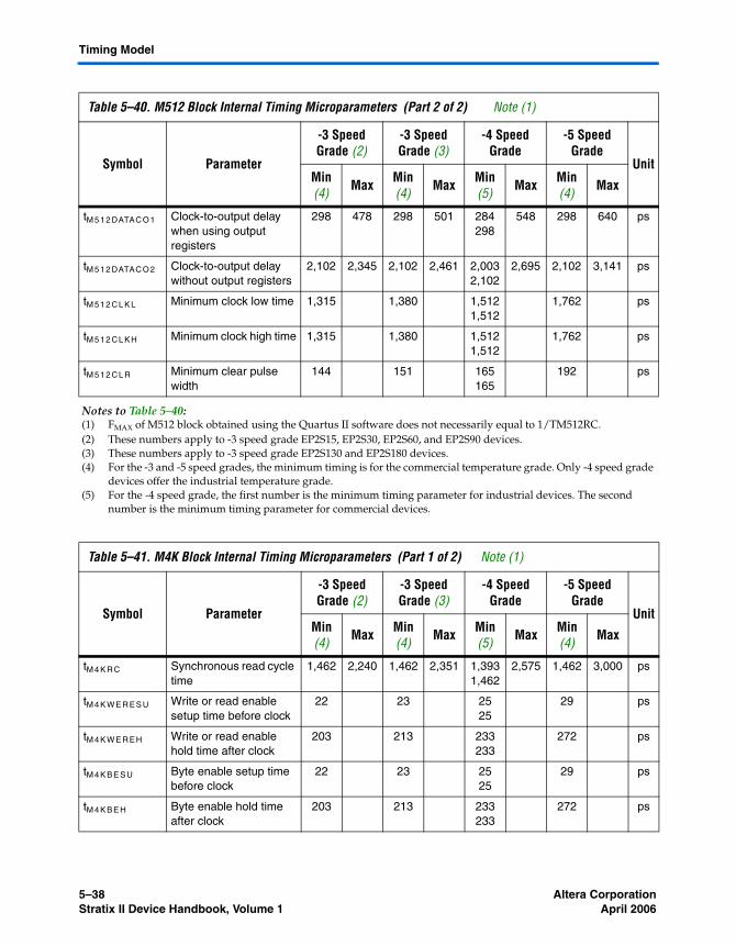
5–38 Altera CorporationStratix II Device Handbook, Volume 1 April 2006
Timing Model
tM 5 1 2 DATAC O 1 Clock-to-output delay when using output registers
298 478 298 501 284298
548 298 640 ps
tM 5 1 2 DATAC O 2 Clock-to-output delay without output registers
2,102 2,345 2,102 2,461 2,0032,102
2,695 2,102 3,141 ps
tM 5 1 2 C L K L Minimum clock low time 1,315 1,380 1,5121,512
1,762 ps
tM 5 1 2 C L K H Minimum clock high time 1,315 1,380 1,5121,512
1,762 ps
tM 5 1 2 C L R Minimum clear pulse width
144 151 165165
192 ps
Notes to Table 5–40:(1) FMAX of M512 block obtained using the Quartus II software does not necessarily equal to 1/TM512RC.(2) These numbers apply to -3 speed grade EP2S15, EP2S30, EP2S60, and EP2S90 devices.(3) These numbers apply to -3 speed grade EP2S130 and EP2S180 devices.(4) For the -3 and -5 speed grades, the minimum timing is for the commercial temperature grade. Only -4 speed grade
devices offer the industrial temperature grade.(5) For the -4 speed grade, the first number is the minimum timing parameter for industrial devices. The second
number is the minimum timing parameter for commercial devices.
Table 5–41. M4K Block Internal Timing Microparameters (Part 1 of 2) Note (1)
Symbol Parameter
-3 Speed Grade (2)
-3 Speed Grade (3)
-4 Speed Grade
-5 Speed Grade
UnitMin (4) Max Min
(4) Max Min (5) Max Min
(4) Max
tM 4 K R C Synchronous read cycle time
1,462 2,240 1,462 2,351 1,3931,462
2,575 1,462 3,000 ps
tM 4 K W E R E S U Write or read enable setup time before clock
22 23 2525
29 ps
tM 4 K W E R E H Write or read enable hold time after clock
203 213 233233
272 ps
tM 4 K B E S U Byte enable setup time before clock
22 23 2525
29 ps
tM 4 K B E H Byte enable hold time after clock
203 213 233233
272 ps
Table 5–40. M512 Block Internal Timing Microparameters (Part 2 of 2) Note (1)
Symbol Parameter
-3 Speed Grade (2)
-3 Speed Grade (3)
-4 Speed Grade
-5 Speed Grade
UnitMin (4) Max Min
(4) Max Min (5) Max Min
(4) Max
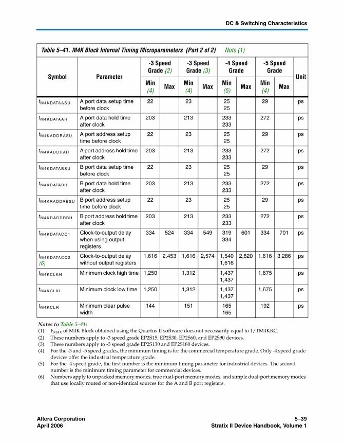
Altera Corporation 5–39April 2006 Stratix II Device Handbook, Volume 1
DC & Switching Characteristics
tM 4 K DATA A S U A port data setup time before clock
22 23 2525
29 ps
tM 4 K DATA A H A port data hold time after clock
203 213 233233
272 ps
tM 4 K A D D R A S U A port address setup time before clock
22 23 2525
29 ps
tM 4 K A D D R A H A port address hold time after clock
203 213 233233
272 ps
tM 4 K DATA B S U B port data setup time before clock
22 23 2525
29 ps
tM 4 K DATA B H B port data hold time after clock
203 213 233233
272 ps
tM4KRADDRBS U B port address setup time before clock
22 23 2525
29 ps
tM 4 K R A D D RB H B port address hold time after clock
203 213 233233
272 ps
tM 4 K DATAC O 1 Clock-to-output delay when using output registers
334 524 334 549 319334
601 334 701 ps
tM 4 K DATAC O 2
(6)Clock-to-output delay without output registers
1,616 2,453 1,616 2,574 1,5401,616
2,820 1,616 3,286 ps
tM 4 K C L K H Minimum clock high time 1,250 1,312 1,4371,437
1,675 ps
tM 4 K C L K L Minimum clock low time 1,250 1,312 1,4371,437
1,675 ps
tM 4 K C L R Minimum clear pulse width
144 151 165165
192 ps
Notes to Table 5–41:(1) FMAX of M4K Block obtained using the Quartus II software does not necessarily equal to 1/TM4KRC.(2) These numbers apply to -3 speed grade EP2S15, EP2S30, EP2S60, and EP2S90 devices.(3) These numbers apply to -3 speed grade EP2S130 and EP2S180 devices.(4) For the -3 and -5 speed grades, the minimum timing is for the commercial temperature grade. Only -4 speed grade
devices offer the industrial temperature grade.(5) For the -4 speed grade, the first number is the minimum timing parameter for industrial devices. The second
number is the minimum timing parameter for commercial devices.(6) Numbers apply to unpacked memory modes, true dual-port memory modes, and simple dual-port memory modes
that use locally routed or non-identical sources for the A and B port registers.
Table 5–41. M4K Block Internal Timing Microparameters (Part 2 of 2) Note (1)
Symbol Parameter
-3 Speed Grade (2)
-3 Speed Grade (3)
-4 Speed Grade
-5 Speed Grade
UnitMin (4) Max Min
(4) Max Min (5) Max Min
(4) Max
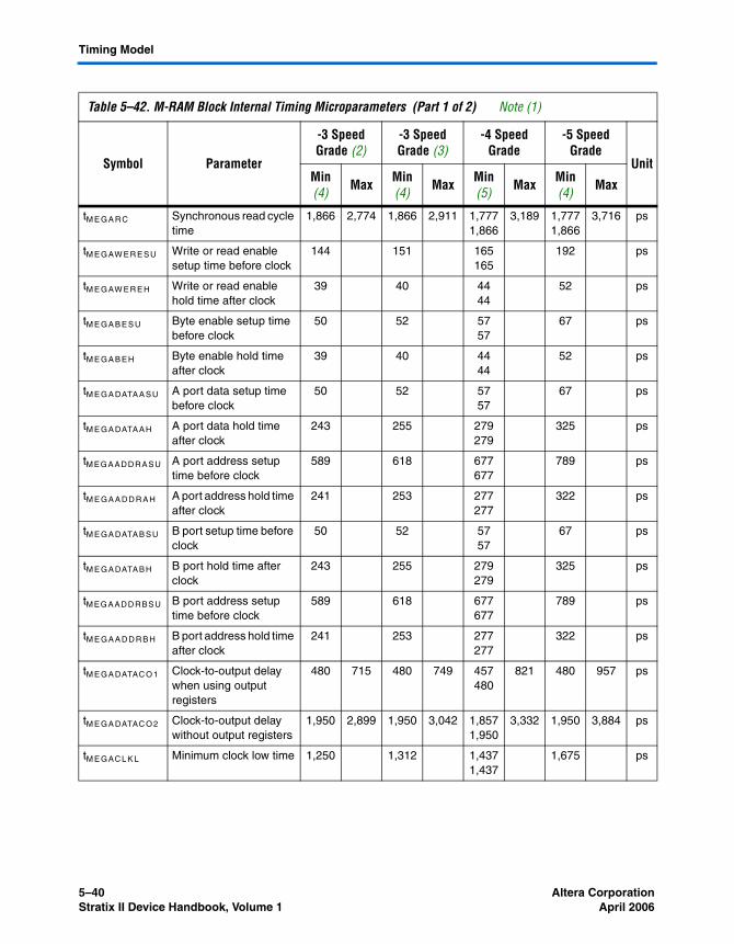
5–40 Altera CorporationStratix II Device Handbook, Volume 1 April 2006
Timing Model
Table 5–42. M-RAM Block Internal Timing Microparameters (Part 1 of 2) Note (1)
Symbol Parameter
-3 Speed Grade (2)
-3 Speed Grade (3)
-4 Speed Grade
-5 Speed Grade
UnitMin (4) Max Min
(4) Max Min (5) Max Min
(4) Max
tM E GA R C Synchronous read cycle time
1,866 2,774 1,866 2,911 1,7771,866
3,189 1,7771,866
3,716 ps
tM E GAW E R E S U Write or read enable setup time before clock
144 151 165165
192 ps
tM E GAW E R E H Write or read enable hold time after clock
39 40 4444
52 ps
tM E GA B E S U Byte enable setup time before clock
50 52 5757
67 ps
tM E GA B E H Byte enable hold time after clock
39 40 4444
52 ps
tM E GA DATA A S U A port data setup time before clock
50 52 5757
67 ps
tM E GA DATA A H A port data hold time after clock
243 255 279279
325 ps
tMEGAADDRASU A port address setup time before clock
589 618 677677
789 ps
tM E GA A DD R A H A port address hold time after clock
241 253 277277
322 ps
tM E GA DATA B S U B port setup time before clock
50 52 5757
67 ps
tM E GA DATA B H B port hold time after clock
243 255 279279
325 ps
tMEGAADDRBSU B port address setup time before clock
589 618 677677
789 ps
tM E GA A DD R B H B port address hold time after clock
241 253 277277
322 ps
tM E GA DATAC O 1 Clock-to-output delay when using output registers
480 715 480 749 457480
821 480 957 ps
tM E GA DATAC O 2 Clock-to-output delay without output registers
1,950 2,899 1,950 3,042 1,8571,950
3,332 1,950 3,884 ps
tM E GAC L K L Minimum clock low time 1,250 1,312 1,4371,437
1,675 ps
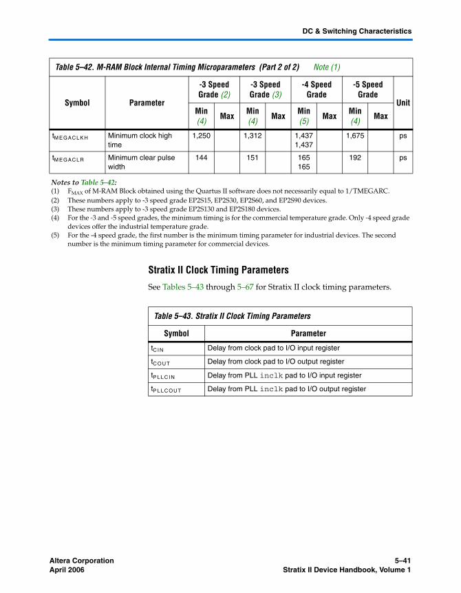
Altera Corporation 5–41April 2006 Stratix II Device Handbook, Volume 1
DC & Switching Characteristics
Stratix II Clock Timing Parameters
See Tables 5–43 through 5–67 for Stratix II clock timing parameters.
tM E GAC L K H Minimum clock high time
1,250 1,312 1,4371,437
1,675 ps
tM E GAC L R Minimum clear pulse width
144 151 165165
192 ps
Notes to Table 5–42:(1) FMAX of M-RAM Block obtained using the Quartus II software does not necessarily equal to 1/TMEGARC.(2) These numbers apply to -3 speed grade EP2S15, EP2S30, EP2S60, and EP2S90 devices.(3) These numbers apply to -3 speed grade EP2S130 and EP2S180 devices.(4) For the -3 and -5 speed grades, the minimum timing is for the commercial temperature grade. Only -4 speed grade
devices offer the industrial temperature grade.(5) For the -4 speed grade, the first number is the minimum timing parameter for industrial devices. The second
number is the minimum timing parameter for commercial devices.
Table 5–42. M-RAM Block Internal Timing Microparameters (Part 2 of 2) Note (1)
Symbol Parameter
-3 Speed Grade (2)
-3 Speed Grade (3)
-4 Speed Grade
-5 Speed Grade
UnitMin (4) Max Min
(4) Max Min (5) Max Min
(4) Max
Table 5–43. Stratix II Clock Timing Parameters
Symbol Parameter
tC I N Delay from clock pad to I/O input register
tC O UT Delay from clock pad to I/O output register
tP L L C I N Delay from PLL inclk pad to I/O input register
tP L L C O U T Delay from PLL inclk pad to I/O output register
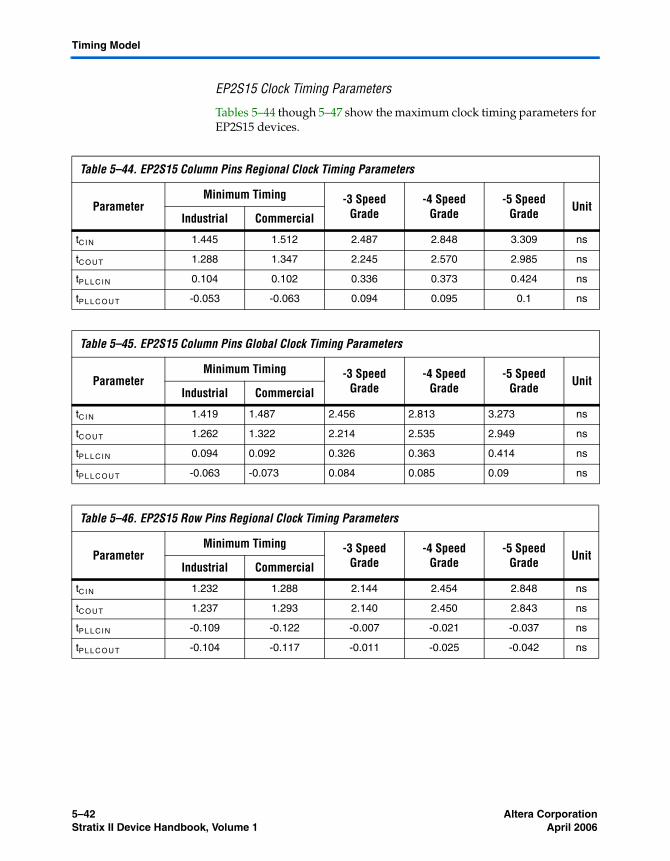
5–42 Altera CorporationStratix II Device Handbook, Volume 1 April 2006
Timing Model
EP2S15 Clock Timing Parameters
Tables 5–44 though 5–47 show the maximum clock timing parameters for EP2S15 devices.
Table 5–44. EP2S15 Column Pins Regional Clock Timing Parameters
ParameterMinimum Timing -3 Speed
Grade-4 Speed
Grade-5 Speed
Grade UnitIndustrial Commercial
tC I N 1.445 1.512 2.487 2.848 3.309 ns
tC O UT 1.288 1.347 2.245 2.570 2.985 ns
tP L L C I N 0.104 0.102 0.336 0.373 0.424 ns
tP L L C O UT -0.053 -0.063 0.094 0.095 0.1 ns
Table 5–45. EP2S15 Column Pins Global Clock Timing Parameters
ParameterMinimum Timing -3 Speed
Grade-4 Speed
Grade-5 Speed
Grade UnitIndustrial Commercial
tC I N 1.419 1.487 2.456 2.813 3.273 ns
tC O UT 1.262 1.322 2.214 2.535 2.949 ns
tP L L C I N 0.094 0.092 0.326 0.363 0.414 ns
tP L L C O UT -0.063 -0.073 0.084 0.085 0.09 ns
Table 5–46. EP2S15 Row Pins Regional Clock Timing Parameters
ParameterMinimum Timing -3 Speed
Grade-4 Speed
Grade-5 Speed
Grade UnitIndustrial Commercial
tC I N 1.232 1.288 2.144 2.454 2.848 ns
tC O UT 1.237 1.293 2.140 2.450 2.843 ns
tP L L C I N -0.109 -0.122 -0.007 -0.021 -0.037 ns
tP L L C O UT -0.104 -0.117 -0.011 -0.025 -0.042 ns
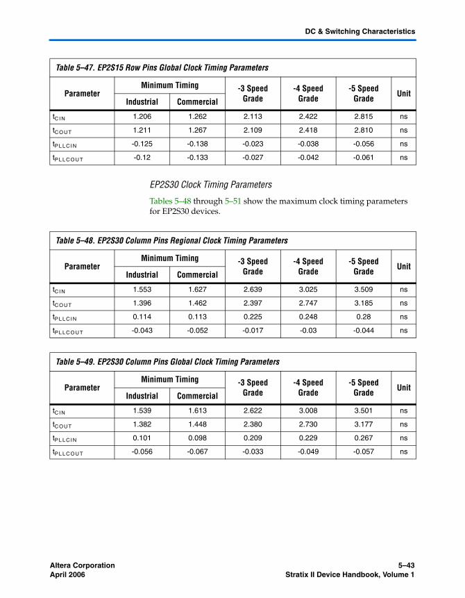
Altera Corporation 5–43April 2006 Stratix II Device Handbook, Volume 1
DC & Switching Characteristics
EP2S30 Clock Timing Parameters
Tables 5–48 through 5–51 show the maximum clock timing parameters for EP2S30 devices.
Table 5–47. EP2S15 Row Pins Global Clock Timing Parameters
ParameterMinimum Timing -3 Speed
Grade-4 Speed
Grade-5 Speed
Grade UnitIndustrial Commercial
tC I N 1.206 1.262 2.113 2.422 2.815 ns
tC O UT 1.211 1.267 2.109 2.418 2.810 ns
tP L L C I N -0.125 -0.138 -0.023 -0.038 -0.056 ns
tP L L C O UT -0.12 -0.133 -0.027 -0.042 -0.061 ns
Table 5–48. EP2S30 Column Pins Regional Clock Timing Parameters
ParameterMinimum Timing -3 Speed
Grade-4 Speed
Grade-5 Speed
Grade UnitIndustrial Commercial
tC I N 1.553 1.627 2.639 3.025 3.509 ns
tC O UT 1.396 1.462 2.397 2.747 3.185 ns
tP L L C I N 0.114 0.113 0.225 0.248 0.28 ns
tP L L C O UT -0.043 -0.052 -0.017 -0.03 -0.044 ns
Table 5–49. EP2S30 Column Pins Global Clock Timing Parameters
ParameterMinimum Timing -3 Speed
Grade-4 Speed
Grade-5 Speed
Grade UnitIndustrial Commercial
tC I N 1.539 1.613 2.622 3.008 3.501 ns
tC O UT 1.382 1.448 2.380 2.730 3.177 ns
tP L L C I N 0.101 0.098 0.209 0.229 0.267 ns
tP L L C O UT -0.056 -0.067 -0.033 -0.049 -0.057 ns
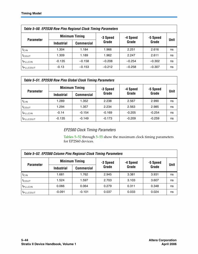
5–44 Altera CorporationStratix II Device Handbook, Volume 1 April 2006
Timing Model
EP2S60 Clock Timing Parameters
Tables 5–52 through 5–55 show the maximum clock timing parameters for EP2S60 devices.
Table 5–50. EP2S30 Row Pins Regional Clock Timing Parameters
ParameterMinimum Timing -3 Speed
Grade-4 Speed
Grade-5 Speed
Grade UnitIndustrial Commercial
tC I N 1.304 1.184 1.966 2.251 2.616 ns
tC O UT 1.309 1.189 1.962 2.247 2.611 ns
tP L L C I N -0.135 –0.158 –0.208 –0.254 –0.302 ns
tP L L C O UT -0.13 –0.153 –0.212 –0.258 –0.307 ns
Table 5–51. EP2S30 Row Pins Global Clock Timing Parameters
ParameterMinimum Timing -3 Speed
Grade-4 Speed
Grade-5 Speed
Grade UnitIndustrial Commercial
tC I N 1.289 1.352 2.238 2.567 2.990 ns
tC O UT 1.294 1.357 2.234 2.563 2.985 ns
tP L L C I N -0.14 -0.154 -0.169 -0.205 -0.254 ns
tP L L C O UT -0.135 -0.149 -0.173 -0.209 -0.259 ns
Table 5–52. EP2S60 Column Pins Regional Clock Timing Parameters
ParameterMinimum Timing -3 Speed
Grade-4 Speed
Grade-5 Speed
Grade UnitIndustrial Commercial
tC I N 1.681 1.762 2.945 3.381 3.931 ns
tC O UT 1.524 1.597 2.703 3.103 3.607 ns
tP L L C I N 0.066 0.064 0.279 0.311 0.348 ns
tP L L C O UT -0.091 -0.101 0.037 0.033 0.024 ns
Altera Corporation 5–45April 2006 Stratix II Device Handbook, Volume 1
DC & Switching Characteristics
Table 5–53. EP2S60 Column Pins Global Clock Timing Parameters
ParameterMinimum Timing -3 Speed
Grade-4 Speed
Grade-5 Speed
Grade UnitIndustrial Commercial
tC I N 1.658 1.739 2.920 3.350 3.899 ns
tC O UT 1.501 1.574 2.678 3.072 3.575 ns
tP L L C I N 0.06 0.057 0.278 0.304 0.355 ns
tP L L C O UT -0.097 -0.108 0.036 0.026 0.031 ns
Table 5–54. EP2S60 Row Pins Regional Clock Timing Parameters
ParameterMinimum Timing -3 Speed
Grade-4 Speed
Grade-5 Speed
Grade UnitIndustrial Commercial
tC I N 1.463 1.532 2.591 2.972 3.453 ns
tC O UT 1.468 1.537 2.587 2.968 3.448 ns
tP L L C I N -0.153 -0.167 -0.079 -0.099 -0.128 ns
tP L L C O UT -0.148 -0.162 -0.083 -0.103 -0.133 ns
Table 5–55. EP2S60 Row Pins Global Clock Timing Parameters
ParameterMinimum Timing -3 Speed
Grade-4 Speed
Grade-5 Speed
Grade UnitIndustrial Commercial
tC I N 1.439 1.508 2.562 2.940 3.421 ns
tC O UT 1.444 1.513 2.558 2.936 3.416 ns
tP L L C I N -0.161 -0.174 -0.083 -0.107 -0.126 ns
tP L L C O UT -0.156 -0.169 -0.087 -0.111 -0.131 ns
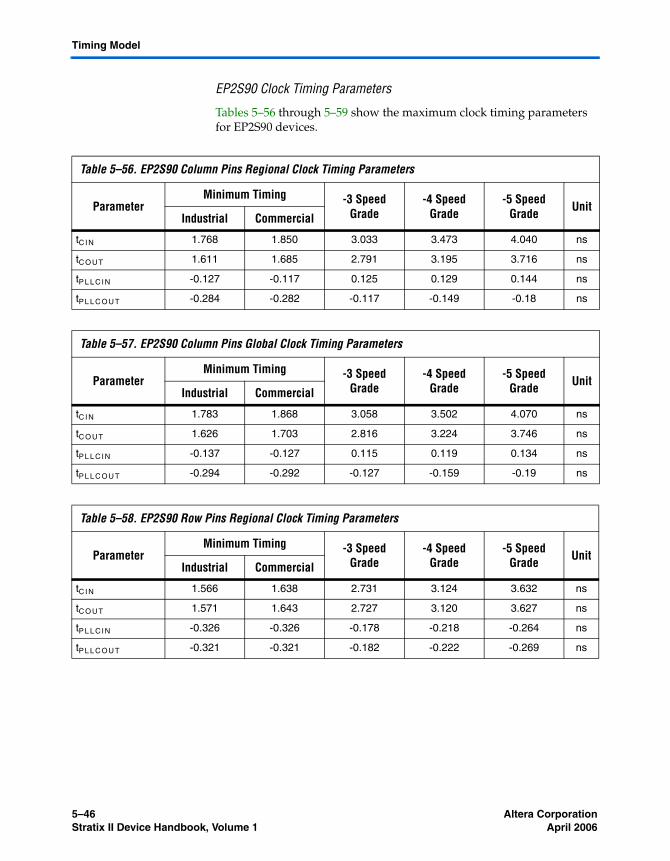
5–46 Altera CorporationStratix II Device Handbook, Volume 1 April 2006
Timing Model
EP2S90 Clock Timing Parameters
Tables 5–56 through 5–59 show the maximum clock timing parameters for EP2S90 devices.
Table 5–56. EP2S90 Column Pins Regional Clock Timing Parameters
ParameterMinimum Timing -3 Speed
Grade-4 Speed
Grade-5 Speed
Grade UnitIndustrial Commercial
tC I N 1.768 1.850 3.033 3.473 4.040 ns
tC O UT 1.611 1.685 2.791 3.195 3.716 ns
tP L L C I N -0.127 -0.117 0.125 0.129 0.144 ns
tP L L C O UT -0.284 -0.282 -0.117 -0.149 -0.18 ns
Table 5–57. EP2S90 Column Pins Global Clock Timing Parameters
ParameterMinimum Timing -3 Speed
Grade-4 Speed
Grade-5 Speed
Grade UnitIndustrial Commercial
tC I N 1.783 1.868 3.058 3.502 4.070 ns
tC O UT 1.626 1.703 2.816 3.224 3.746 ns
tP L L C I N -0.137 -0.127 0.115 0.119 0.134 ns
tP L L C O UT -0.294 -0.292 -0.127 -0.159 -0.19 ns
Table 5–58. EP2S90 Row Pins Regional Clock Timing Parameters
ParameterMinimum Timing -3 Speed
Grade-4 Speed
Grade-5 Speed
Grade UnitIndustrial Commercial
tC I N 1.566 1.638 2.731 3.124 3.632 ns
tC O UT 1.571 1.643 2.727 3.120 3.627 ns
tP L L C I N -0.326 -0.326 -0.178 -0.218 -0.264 ns
tP L L C O UT -0.321 -0.321 -0.182 -0.222 -0.269 ns
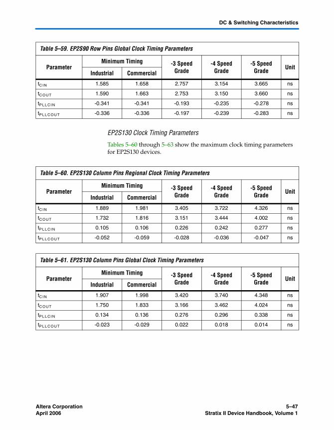
Altera Corporation 5–47April 2006 Stratix II Device Handbook, Volume 1
DC & Switching Characteristics
EP2S130 Clock Timing Parameters
Tables 5–60 through 5–63 show the maximum clock timing parameters for EP2S130 devices.
Table 5–59. EP2S90 Row Pins Global Clock Timing Parameters
ParameterMinimum Timing -3 Speed
Grade-4 Speed
Grade-5 Speed
Grade UnitIndustrial Commercial
tC I N 1.585 1.658 2.757 3.154 3.665 ns
tC O UT 1.590 1.663 2.753 3.150 3.660 ns
tP L L C I N -0.341 -0.341 -0.193 -0.235 -0.278 ns
tP L L C O UT -0.336 -0.336 -0.197 -0.239 -0.283 ns
Table 5–60. EP2S130 Column Pins Regional Clock Timing Parameters
ParameterMinimum Timing -3 Speed
Grade-4 Speed
Grade-5 Speed
Grade UnitIndustrial Commercial
tC I N 1.889 1.981 3.405 3.722 4.326 ns
tC O UT 1.732 1.816 3.151 3.444 4.002 ns
tP L L C I N 0.105 0.106 0.226 0.242 0.277 ns
tP L L C O UT -0.052 -0.059 -0.028 -0.036 -0.047 ns
Table 5–61. EP2S130 Column Pins Global Clock Timing Parameters
ParameterMinimum Timing -3 Speed
Grade-4 Speed
Grade-5 Speed
Grade UnitIndustrial Commercial
tC I N 1.907 1.998 3.420 3.740 4.348 ns
tC O UT 1.750 1.833 3.166 3.462 4.024 ns
tP L L C I N 0.134 0.136 0.276 0.296 0.338 ns
tP L L C O UT -0.023 -0.029 0.022 0.018 0.014 ns
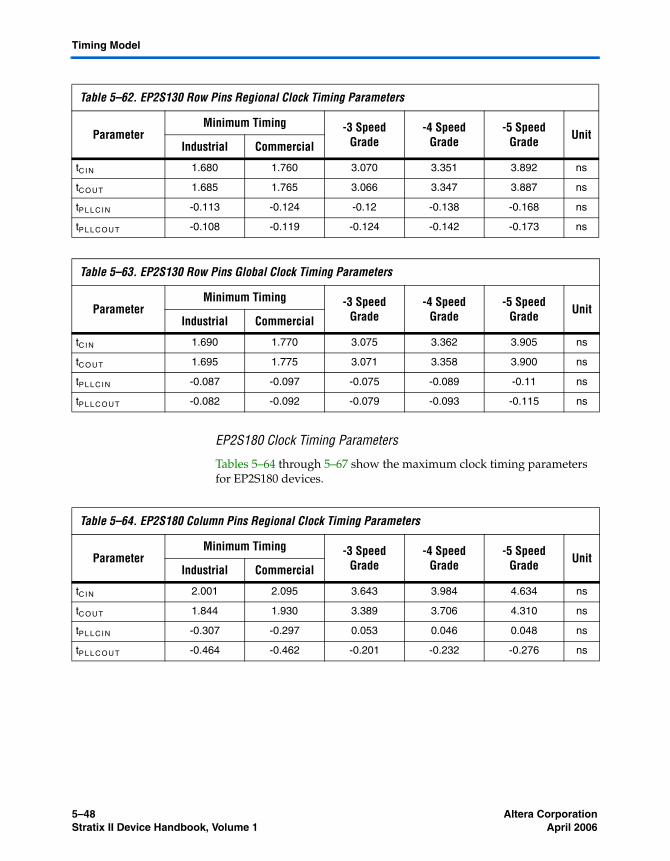
5–48 Altera CorporationStratix II Device Handbook, Volume 1 April 2006
Timing Model
EP2S180 Clock Timing Parameters
Tables 5–64 through 5–67 show the maximum clock timing parameters for EP2S180 devices.
Table 5–62. EP2S130 Row Pins Regional Clock Timing Parameters
ParameterMinimum Timing -3 Speed
Grade-4 Speed
Grade-5 Speed
Grade UnitIndustrial Commercial
tC I N 1.680 1.760 3.070 3.351 3.892 ns
tC O UT 1.685 1.765 3.066 3.347 3.887 ns
tP L L C I N -0.113 -0.124 -0.12 -0.138 -0.168 ns
tP L L C O UT -0.108 -0.119 -0.124 -0.142 -0.173 ns
Table 5–63. EP2S130 Row Pins Global Clock Timing Parameters
ParameterMinimum Timing -3 Speed
Grade-4 Speed
Grade-5 Speed
Grade UnitIndustrial Commercial
tC I N 1.690 1.770 3.075 3.362 3.905 ns
tC O UT 1.695 1.775 3.071 3.358 3.900 ns
tP L L C I N -0.087 -0.097 -0.075 -0.089 -0.11 ns
tP L L C O UT -0.082 -0.092 -0.079 -0.093 -0.115 ns
Table 5–64. EP2S180 Column Pins Regional Clock Timing Parameters
ParameterMinimum Timing -3 Speed
Grade-4 Speed
Grade-5 Speed
Grade UnitIndustrial Commercial
tC I N 2.001 2.095 3.643 3.984 4.634 ns
tC O UT 1.844 1.930 3.389 3.706 4.310 ns
tP L L C I N -0.307 -0.297 0.053 0.046 0.048 ns
tP L L C O UT -0.464 -0.462 -0.201 -0.232 -0.276 ns
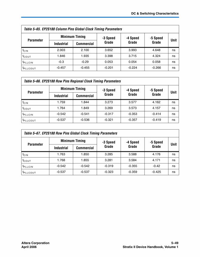
Altera Corporation 5–49April 2006 Stratix II Device Handbook, Volume 1
DC & Switching Characteristics
Table 5–65. EP2S180 Column Pins Global Clock Timing Parameters
ParameterMinimum Timing -3 Speed
Grade-4 Speed
Grade-5 Speed
Grade UnitIndustrial Commercial
tC I N 2.003 2.100 3.652 3.993 4.648 ns
tC O UT 1.846 1.935 3.398 3.715 4.324 ns
tP L L C I N -0.3 -0.29 0.053 0.054 0.058 ns
tP L L C O UT -0.457 -0.455 -0.201 -0.224 -0.266 ns
Table 5–66. EP2S180 Row Pins Regional Clock Timing Parameters
ParameterMinimum Timing -3 Speed
Grade-4 Speed
Grade-5 Speed
Grade UnitIndustrial Commercial
tC I N 1.759 1.844 3.273 3.577 4.162 ns
tC O UT 1.764 1.849 3.269 3.573 4.157 ns
tP L L C I N -0.542 -0.541 -0.317 -0.353 -0.414 ns
tP L L C O UT -0.537 -0.536 -0.321 -0.357 -0.419 ns
Table 5–67. EP2S180 Row Pins Global Clock Timing Parameters
ParameterMinimum Timing -3 Speed
Grade-4 Speed
Grade-5 Speed
Grade UnitIndustrial Commercial
tC I N 1.763 1.850 3.285 3.588 4.176 ns
tC O UT 1.768 1.855 3.281 3.584 4.171 ns
tP L L C I N -0.542 -0.542 -0.319 -0.355 -0.42 ns
tP L L C O UT -0.537 -0.537 -0.323 -0.359 -0.425 ns
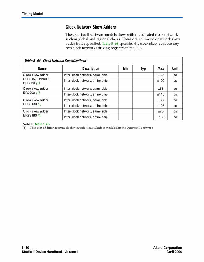
5–50 Altera CorporationStratix II Device Handbook, Volume 1 April 2006
Timing Model
Clock Network Skew Adders
The Quartus II software models skew within dedicated clock networks such as global and regional clocks. Therefore, intra-clock network skew adder is not specified. Table 5–68 specifies the clock skew between any two clock networks driving registers in the IOE.
Table 5–68. Clock Network Specifications
Name Description Min Typ Max Unit
Clock skew adderEP2S15, EP2S30, EP2S60 (1)
Inter-clock network, same side ±50 ps
Inter-clock network, entire chip ±100 ps
Clock skew adderEP2S90 (1)
Inter-clock network, same side ±55 ps
Inter-clock network, entire chip ±110 ps
Clock skew adderEP2S130 (1)
Inter-clock network, same side ±63 ps
Inter-clock network, entire chip ±125 ps
Clock skew adderEP2S180 (1)
Inter-clock network, same side ±75 ps
Inter-clock network, entire chip ±150 ps
Note to Table 5–68:(1) This is in addition to intra-clock network skew, which is modeled in the Quartus II software.
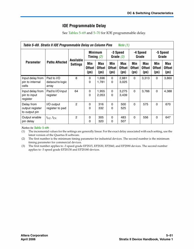
Altera Corporation 5–51April 2006 Stratix II Device Handbook, Volume 1
DC & Switching Characteristics
IOE Programmable Delay
See Tables 5–69 and 5–70 for IOE programmable delay.
Table 5–69. Stratix II IOE Programmable Delay on Column Pins Note (1)
Parameter Paths Affected Available Settings
Minimum Timing (2)
-3 Speed Grade (3)
-4 Speed Grade
-5 Speed Grade
Min Offset (ps)
Max Offset (ps)
Min Offset (ps)
Max Offset (ps)
Min Offset (ps)
Max Offset (ps)
Min Offset (ps)
Max Offset (ps)
Input delay from pin to internal cells
Pad to I/O dataout to logic array
8 00
1,6961,781
00
2,8813,025
0 3,313 0 3,860
Input delay from pin to input register
Pad to I/O input register
64 00
1,9552,053
00
3,2753,439
0 3,766 0 4,388
Delay from output register to output pin
I/O output register to pad
2 00
316332
00
500525
0 575 0 670
Output enable pin delay
tX Z, tZ X 2 00
305320
00
483507
0 556 0 647
Notes to Table 5–69:(1) The incremental values for the settings are generally linear. For the exact delay associated with each setting, use the
latest version of the Quartus II software.(2) The first number is the minimum timing parameter for industrial devices. The second number is the minimum
timing parameter for commercial devices.(3) The first number applies to -3 speed grade EP2S15, EP2S30, EP2S60, and EP2S90 devices. The second number
applies to -3 speed grade EP2S130 and EP2S180 devices.
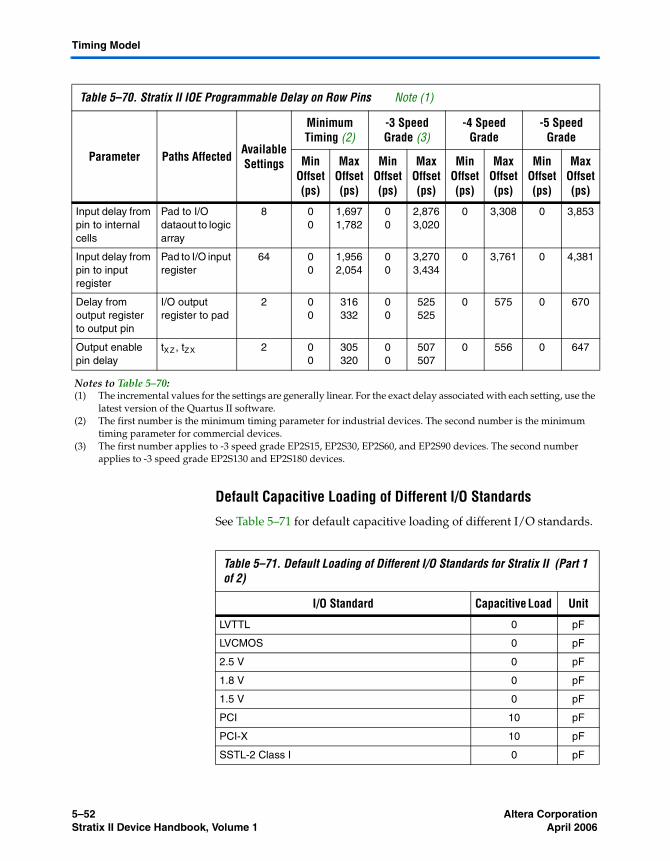
5–52 Altera CorporationStratix II Device Handbook, Volume 1 April 2006
Timing Model
Default Capacitive Loading of Different I/O Standards
See Table 5–71 for default capacitive loading of different I/O standards.
Table 5–70. Stratix II IOE Programmable Delay on Row Pins Note (1)
Parameter Paths Affected Available Settings
Minimum Timing (2)
-3 Speed Grade (3)
-4 Speed Grade
-5 Speed Grade
Min Offset (ps)
Max Offset (ps)
Min Offset (ps)
Max Offset (ps)
Min Offset (ps)
Max Offset (ps)
Min Offset (ps)
Max Offset (ps)
Input delay from pin to internal cells
Pad to I/O dataout to logic array
8 00
1,6971,782
00
2,8763,020
0 3,308 0 3,853
Input delay from pin to input register
Pad to I/O input register
64 00
1,9562,054
00
3,2703,434
0 3,761 0 4,381
Delay from output register to output pin
I/O output register to pad
2 00
316332
00
525525
0 575 0 670
Output enable pin delay
tX Z , tZ X 2 00
305320
00
507507
0 556 0 647
Notes to Table 5–70:(1) The incremental values for the settings are generally linear. For the exact delay associated with each setting, use the
latest version of the Quartus II software.(2) The first number is the minimum timing parameter for industrial devices. The second number is the minimum
timing parameter for commercial devices.(3) The first number applies to -3 speed grade EP2S15, EP2S30, EP2S60, and EP2S90 devices. The second number
applies to -3 speed grade EP2S130 and EP2S180 devices.
Table 5–71. Default Loading of Different I/O Standards for Stratix II (Part 1 of 2)
I/O Standard Capacitive Load Unit
LVTTL 0 pF
LVCMOS 0 pF
2.5 V 0 pF
1.8 V 0 pF
1.5 V 0 pF
PCI 10 pF
PCI-X 10 pF
SSTL-2 Class I 0 pF
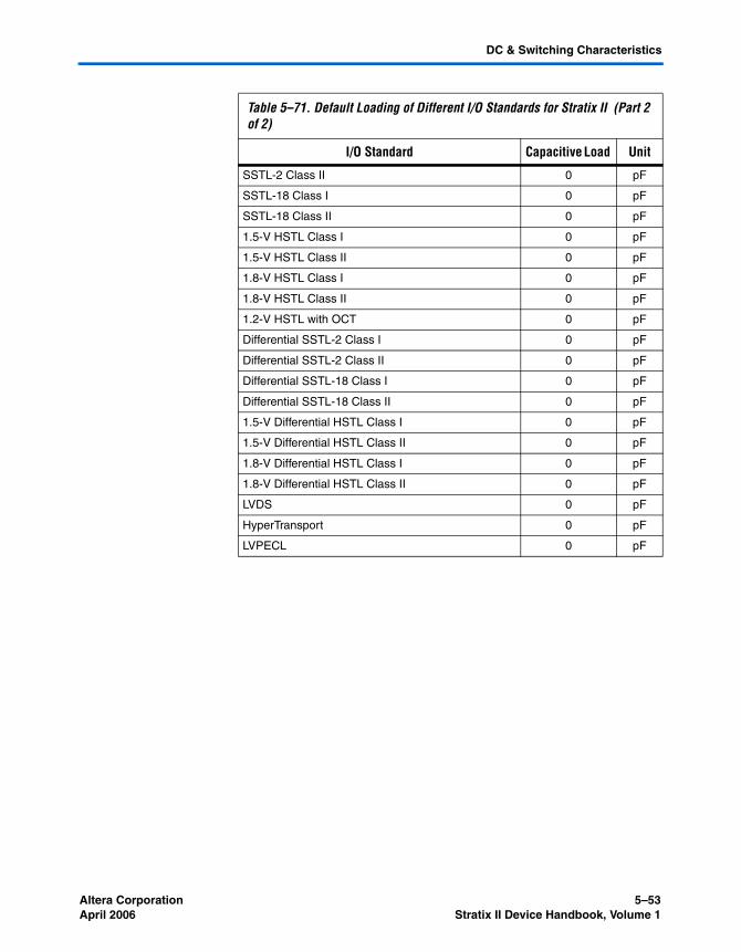
Altera Corporation 5–53April 2006 Stratix II Device Handbook, Volume 1
DC & Switching Characteristics
SSTL-2 Class II 0 pF
SSTL-18 Class I 0 pF
SSTL-18 Class II 0 pF
1.5-V HSTL Class I 0 pF
1.5-V HSTL Class II 0 pF
1.8-V HSTL Class I 0 pF
1.8-V HSTL Class II 0 pF
1.2-V HSTL with OCT 0 pF
Differential SSTL-2 Class I 0 pF
Differential SSTL-2 Class II 0 pF
Differential SSTL-18 Class I 0 pF
Differential SSTL-18 Class II 0 pF
1.5-V Differential HSTL Class I 0 pF
1.5-V Differential HSTL Class II 0 pF
1.8-V Differential HSTL Class I 0 pF
1.8-V Differential HSTL Class II 0 pF
LVDS 0 pF
HyperTransport 0 pF
LVPECL 0 pF
Table 5–71. Default Loading of Different I/O Standards for Stratix II (Part 2 of 2)
I/O Standard Capacitive Load Unit
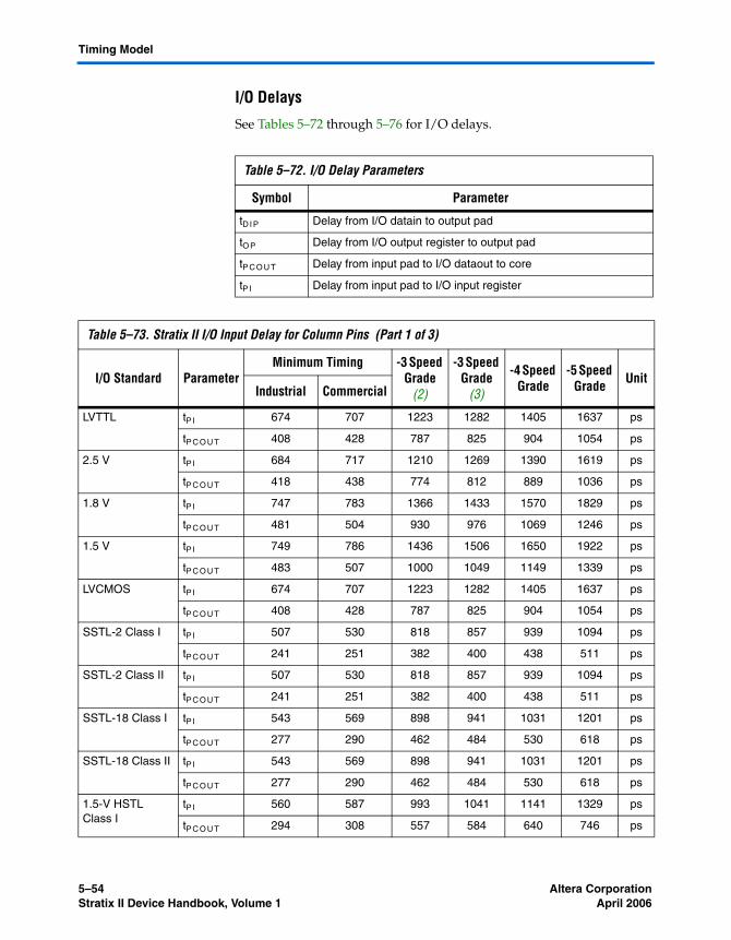
5–54 Altera CorporationStratix II Device Handbook, Volume 1 April 2006
Timing Model
I/O Delays
See Tables 5–72 through 5–76 for I/O delays.
Table 5–72. I/O Delay Parameters
Symbol Parameter
tD I P Delay from I/O datain to output pad
tO P Delay from I/O output register to output pad
tP CO U T Delay from input pad to I/O dataout to core
tP I Delay from input pad to I/O input register
Table 5–73. Stratix II I/O Input Delay for Column Pins (Part 1 of 3)
I/O Standard ParameterMinimum Timing -3 Speed
Grade (2)
-3 Speed Grade
(3)
-4 Speed Grade
-5 Speed Grade Unit
Industrial Commercial
LVTTL tP I 674 707 1223 1282 1405 1637 ps
tP C O U T 408 428 787 825 904 1054 ps
2.5 V tP I 684 717 1210 1269 1390 1619 ps
tP C O U T 418 438 774 812 889 1036 ps
1.8 V tP I 747 783 1366 1433 1570 1829 ps
tP C O U T 481 504 930 976 1069 1246 ps
1.5 V tP I 749 786 1436 1506 1650 1922 ps
tP C O U T 483 507 1000 1049 1149 1339 ps
LVCMOS tP I 674 707 1223 1282 1405 1637 ps
tP C O U T 408 428 787 825 904 1054 ps
SSTL-2 Class I tP I 507 530 818 857 939 1094 ps
tP C O U T 241 251 382 400 438 511 ps
SSTL-2 Class II tP I 507 530 818 857 939 1094 ps
tP C O U T 241 251 382 400 438 511 ps
SSTL-18 Class I tP I 543 569 898 941 1031 1201 ps
tP C O U T 277 290 462 484 530 618 ps
SSTL-18 Class II tP I 543 569 898 941 1031 1201 ps
tP C O U T 277 290 462 484 530 618 ps
1.5-V HSTL Class I
tP I 560 587 993 1041 1141 1329 ps
tP C O U T 294 308 557 584 640 746 ps
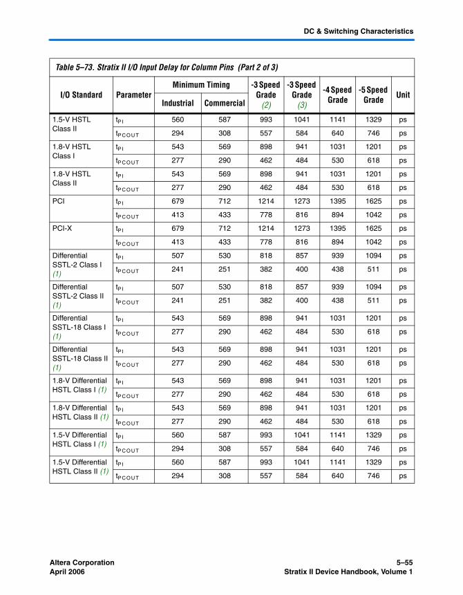
Altera Corporation 5–55April 2006 Stratix II Device Handbook, Volume 1
DC & Switching Characteristics
1.5-V HSTL Class II
tP I 560 587 993 1041 1141 1329 ps
tP C O U T 294 308 557 584 640 746 ps
1.8-V HSTL Class I
tP I 543 569 898 941 1031 1201 ps
tP C O U T 277 290 462 484 530 618 ps
1.8-V HSTL Class II
tP I 543 569 898 941 1031 1201 ps
tP C O U T 277 290 462 484 530 618 ps
PCI tP I 679 712 1214 1273 1395 1625 ps
tP C O U T 413 433 778 816 894 1042 ps
PCI-X tP I 679 712 1214 1273 1395 1625 ps
tP C O U T 413 433 778 816 894 1042 ps
Differential SSTL-2 Class I (1)
tP I 507 530 818 857 939 1094 ps
tP C O U T 241 251 382 400 438 511 ps
Differential SSTL-2 Class II (1)
tP I 507 530 818 857 939 1094 ps
tP C O U T 241 251 382 400 438 511 ps
Differential SSTL-18 Class I (1)
tP I 543 569 898 941 1031 1201 ps
tP C O U T 277 290 462 484 530 618 ps
Differential SSTL-18 Class II (1)
tP I 543 569 898 941 1031 1201 ps
tP C O U T 277 290 462 484 530 618 ps
1.8-V Differential HSTL Class I (1)
tP I 543 569 898 941 1031 1201 ps
tP C O U T 277 290 462 484 530 618 ps
1.8-V Differential HSTL Class II (1)
tP I 543 569 898 941 1031 1201 ps
tP C O U T 277 290 462 484 530 618 ps
1.5-V Differential HSTL Class I (1)
tP I 560 587 993 1041 1141 1329 ps
tP C O U T 294 308 557 584 640 746 ps
1.5-V Differential HSTL Class II (1)
tP I 560 587 993 1041 1141 1329 ps
tP C O U T 294 308 557 584 640 746 ps
Table 5–73. Stratix II I/O Input Delay for Column Pins (Part 2 of 3)
I/O Standard ParameterMinimum Timing -3 Speed
Grade (2)
-3 Speed Grade
(3)
-4 Speed Grade
-5 Speed Grade Unit
Industrial Commercial
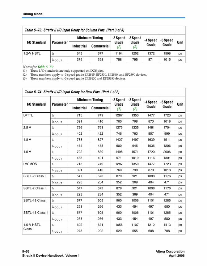
5–56 Altera CorporationStratix II Device Handbook, Volume 1 April 2006
Timing Model
1.2-V HSTL tP I 645 677 1194 1252 1372 1598 ps
tP C O U T 379 398 758 795 871 1015 ps
Notes for Table 5–73:(1) These I/O standards are only supported on DQS pins.(2) These numbers apply to -3 speed grade EP2S15, EP2S30, EP2S60, and EP2S90 devices.(3) These numbers apply to -3 speed grade EP2S130 and EP2S180 devices.
Table 5–74. Stratix II I/O Input Delay for Row Pins (Part 1 of 2)
I/O Standard Parameter Minimum Timing -3 Speed
Grade (1)
-3 Speed Grade
(2)
-4 Speed Grade
-5 Speed Grade Unit
Industrial Commercial
LVTTL tP I 715 749 1287 1350 1477 1723 ps
tP C O U T 391 410 760 798 873 1018 ps
2.5 V tP I 726 761 1273 1335 1461 1704 ps
tP C O U T 402 422 746 783 857 999 ps
1.8 V tP I 788 827 1427 1497 1639 1911 ps
tP C O U T 464 488 900 945 1035 1206 ps
1.5 V tP I 792 830 1498 1571 1720 2006 ps
tP C O U T 468 491 971 1019 1116 1301 ps
LVCMOS tP I 715 749 1287 1350 1477 1723 ps
tP C O U T 391 410 760 798 873 1018 ps
SSTL-2 Class I tP I 547 573 879 921 1008 1176 ps
tP C O U T 223 234 352 369 404 471 ps
SSTL-2 Class II tP I 547 573 879 921 1008 1176 ps
tP C O U T 223 234 352 369 404 471 ps
SSTL-18 Class I tP I 577 605 960 1006 1101 1285 ps
tP C O U T 253 266 433 454 497 580 ps
SSTL-18 Class II tP I 577 605 960 1006 1101 1285 ps
tP C O U T 253 266 433 454 497 580 ps
1.5-V HSTL Class I
tP I 602 631 1056 1107 1212 1413 ps
tP C O U T 278 292 529 555 608 708 ps
Table 5–73. Stratix II I/O Input Delay for Column Pins (Part 3 of 3)
I/O Standard ParameterMinimum Timing -3 Speed
Grade (2)
-3 Speed Grade
(3)
-4 Speed Grade
-5 Speed Grade Unit
Industrial Commercial
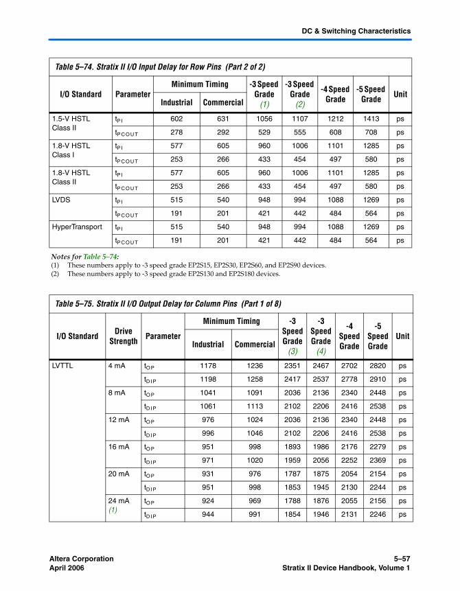
Altera Corporation 5–57April 2006 Stratix II Device Handbook, Volume 1
DC & Switching Characteristics
1.5-V HSTL Class II
tP I 602 631 1056 1107 1212 1413 ps
tP C O U T 278 292 529 555 608 708 ps
1.8-V HSTL Class I
tP I 577 605 960 1006 1101 1285 ps
tP C O U T 253 266 433 454 497 580 ps
1.8-V HSTL Class II
tP I 577 605 960 1006 1101 1285 ps
tP C O U T 253 266 433 454 497 580 ps
LVDS tP I 515 540 948 994 1088 1269 ps
tP C O U T 191 201 421 442 484 564 ps
HyperTransport tP I 515 540 948 994 1088 1269 ps
tP C O U T 191 201 421 442 484 564 ps
Notes for Table 5–74:(1) These numbers apply to -3 speed grade EP2S15, EP2S30, EP2S60, and EP2S90 devices.(2) These numbers apply to -3 speed grade EP2S130 and EP2S180 devices.
Table 5–75. Stratix II I/O Output Delay for Column Pins (Part 1 of 8)
I/O Standard Drive Strength Parameter
Minimum Timing -3 Speed Grade
(3)
-3 Speed Grade
(4)
-4 Speed Grade
-5 Speed Grade
Unit Industrial Commercial
LVTTL 4 mA tO P 1178 1236 2351 2467 2702 2820 ps
tD I P 1198 1258 2417 2537 2778 2910 ps
8 mA tO P 1041 1091 2036 2136 2340 2448 ps
tD I P 1061 1113 2102 2206 2416 2538 ps
12 mA tO P 976 1024 2036 2136 2340 2448 ps
tD I P 996 1046 2102 2206 2416 2538 ps
16 mA tO P 951 998 1893 1986 2176 2279 ps
tD I P 971 1020 1959 2056 2252 2369 ps
20 mA tO P 931 976 1787 1875 2054 2154 ps
tD I P 951 998 1853 1945 2130 2244 ps
24 mA (1)
tO P 924 969 1788 1876 2055 2156 ps
tD I P 944 991 1854 1946 2131 2246 ps
Table 5–74. Stratix II I/O Input Delay for Row Pins (Part 2 of 2)
I/O Standard Parameter Minimum Timing -3 Speed
Grade (1)
-3 Speed Grade
(2)
-4 Speed Grade
-5 Speed Grade Unit
Industrial Commercial
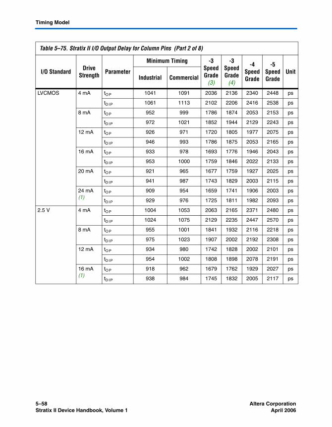
5–58 Altera CorporationStratix II Device Handbook, Volume 1 April 2006
Timing Model
LVCMOS 4 mA tO P 1041 1091 2036 2136 2340 2448 ps
tD I P 1061 1113 2102 2206 2416 2538 ps
8 mA tO P 952 999 1786 1874 2053 2153 ps
tD I P 972 1021 1852 1944 2129 2243 ps
12 mA tO P 926 971 1720 1805 1977 2075 ps
tD I P 946 993 1786 1875 2053 2165 ps
16 mA tO P 933 978 1693 1776 1946 2043 ps
tD I P 953 1000 1759 1846 2022 2133 ps
20 mA tO P 921 965 1677 1759 1927 2025 ps
tD I P 941 987 1743 1829 2003 2115 ps
24 mA (1)
tO P 909 954 1659 1741 1906 2003 ps
tD I P 929 976 1725 1811 1982 2093 ps
2.5 V 4 mA tO P 1004 1053 2063 2165 2371 2480 ps
tD I P 1024 1075 2129 2235 2447 2570 ps
8 mA tO P 955 1001 1841 1932 2116 2218 ps
tD I P 975 1023 1907 2002 2192 2308 ps
12 mA tO P 934 980 1742 1828 2002 2101 ps
tD I P 954 1002 1808 1898 2078 2191 ps
16 mA (1)
tO P 918 962 1679 1762 1929 2027 ps
tD I P 938 984 1745 1832 2005 2117 ps
Table 5–75. Stratix II I/O Output Delay for Column Pins (Part 2 of 8)
I/O Standard Drive Strength Parameter
Minimum Timing -3 Speed Grade
(3)
-3 Speed Grade
(4)
-4 Speed Grade
-5 Speed Grade
Unit Industrial Commercial
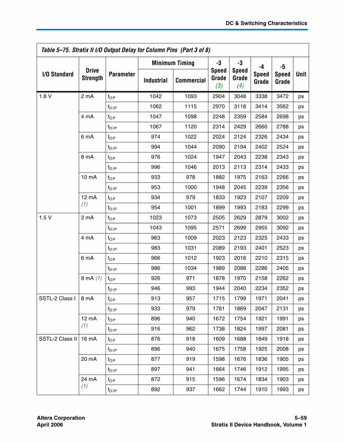
Altera Corporation 5–59April 2006 Stratix II Device Handbook, Volume 1
DC & Switching Characteristics
1.8 V 2 mA tO P 1042 1093 2904 3048 3338 3472 ps
tD I P 1062 1115 2970 3118 3414 3562 ps
4 mA tO P 1047 1098 2248 2359 2584 2698 ps
tD I P 1067 1120 2314 2429 2660 2788 ps
6 mA tO P 974 1022 2024 2124 2326 2434 ps
tD I P 994 1044 2090 2194 2402 2524 ps
8 mA tO P 976 1024 1947 2043 2238 2343 ps
tD I P 996 1046 2013 2113 2314 2433 ps
10 mA tO P 933 978 1882 1975 2163 2266 ps
tD I P 953 1000 1948 2045 2239 2356 ps
12 mA (1)
tO P 934 979 1833 1923 2107 2209 ps
tD I P 954 1001 1899 1993 2183 2299 ps
1.5 V 2 mA tO P 1023 1073 2505 2629 2879 3002 ps
tD I P 1043 1095 2571 2699 2955 3092 ps
4 mA tO P 963 1009 2023 2123 2325 2433 ps
tD I P 983 1031 2089 2193 2401 2523 ps
6 mA tO P 966 1012 1923 2018 2210 2315 ps
tD I P 986 1034 1989 2088 2286 2405 ps
8 mA (1) tO P 926 971 1878 1970 2158 2262 ps
tD I P 946 993 1944 2040 2234 2352 ps
SSTL-2 Class I 8 mA tO P 913 957 1715 1799 1971 2041 ps
tD I P 933 979 1781 1869 2047 2131 ps
12 mA (1)
tO P 896 940 1672 1754 1921 1991 ps
tD I P 916 962 1738 1824 1997 2081 ps
SSTL-2 Class II 16 mA tO P 876 918 1609 1688 1849 1918 ps
tD I P 896 940 1675 1758 1925 2008 ps
20 mA tO P 877 919 1598 1676 1836 1905 ps
tD I P 897 941 1664 1746 1912 1995 ps
24 mA (1)
tO P 872 915 1596 1674 1834 1903 ps
tD I P 892 937 1662 1744 1910 1993 ps
Table 5–75. Stratix II I/O Output Delay for Column Pins (Part 3 of 8)
I/O Standard Drive Strength Parameter
Minimum Timing -3 Speed Grade
(3)
-3 Speed Grade
(4)
-4 Speed Grade
-5 Speed Grade
Unit Industrial Commercial
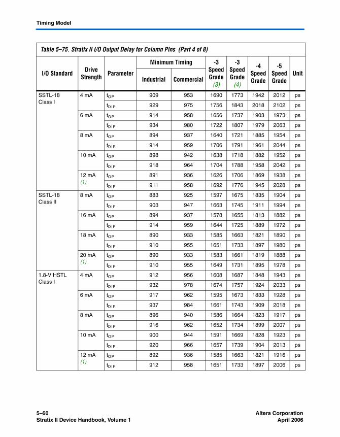
5–60 Altera CorporationStratix II Device Handbook, Volume 1 April 2006
Timing Model
SSTL-18 Class I
4 mA tO P 909 953 1690 1773 1942 2012 ps
tD I P 929 975 1756 1843 2018 2102 ps
6 mA tO P 914 958 1656 1737 1903 1973 ps
tD I P 934 980 1722 1807 1979 2063 ps
8 mA tO P 894 937 1640 1721 1885 1954 ps
tD I P 914 959 1706 1791 1961 2044 ps
10 mA tO P 898 942 1638 1718 1882 1952 ps
tD I P 918 964 1704 1788 1958 2042 ps
12 mA (1)
tO P 891 936 1626 1706 1869 1938 ps
tD I P 911 958 1692 1776 1945 2028 ps
SSTL-18 Class II
8 mA tO P 883 925 1597 1675 1835 1904 ps
tD I P 903 947 1663 1745 1911 1994 ps
16 mA tO P 894 937 1578 1655 1813 1882 ps
tD I P 914 959 1644 1725 1889 1972 ps
18 mA tO P 890 933 1585 1663 1821 1890 ps
tD I P 910 955 1651 1733 1897 1980 ps
20 mA (1)
tO P 890 933 1583 1661 1819 1888 ps
tD I P 910 955 1649 1731 1895 1978 ps
1.8-V HSTL Class I
4 mA tO P 912 956 1608 1687 1848 1943 ps
tD I P 932 978 1674 1757 1924 2033 ps
6 mA tO P 917 962 1595 1673 1833 1928 ps
tD I P 937 984 1661 1743 1909 2018 ps
8 mA tO P 896 940 1586 1664 1823 1917 ps
tD I P 916 962 1652 1734 1899 2007 ps
10 mA tO P 900 944 1591 1669 1828 1923 ps
tD I P 920 966 1657 1739 1904 2013 ps
12 mA (1)
tO P 892 936 1585 1663 1821 1916 ps
tD I P 912 958 1651 1733 1897 2006 ps
Table 5–75. Stratix II I/O Output Delay for Column Pins (Part 4 of 8)
I/O Standard Drive Strength Parameter
Minimum Timing -3 Speed Grade
(3)
-3 Speed Grade
(4)
-4 Speed Grade
-5 Speed Grade
Unit Industrial Commercial
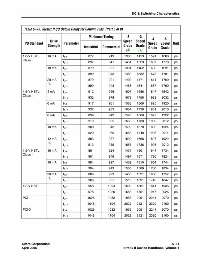
Altera Corporation 5–61April 2006 Stratix II Device Handbook, Volume 1
DC & Switching Characteristics
1.8-V HSTL Class II
16 mA tO P 877 919 1385 1453 1591 1680 ps
tD I P 897 941 1451 1523 1667 1770 ps
18 mA tO P 879 921 1394 1462 1602 1691 ps
tD I P 899 943 1460 1532 1678 1781 ps
20 mA (1)
tO P 879 921 1402 1471 1611 1700 ps
tD I P 899 943 1468 1541 1687 1790 ps
1.5-V HSTL Class I
4 mA tO P 912 956 1607 1686 1847 1942 ps
tD I P 932 978 1673 1756 1923 2032 ps
6 mA tO P 917 961 1588 1666 1825 1920 ps
tD I P 937 983 1654 1736 1901 2010 ps
8 mA tO P 899 943 1590 1668 1827 1922 ps
tD I P 919 965 1656 1738 1903 2012 ps
10 mA tO P 900 943 1592 1670 1829 1924 ps
tD I P 920 965 1658 1740 1905 2014 ps
12 mA (1)
tO P 893 937 1590 1668 1827 1922 ps
tD I P 913 959 1656 1738 1903 2012 ps
1.5-V HSTL Class II
16 mA tO P 881 924 1431 1501 1644 1734 ps
tD I P 901 946 1497 1571 1720 1824 ps
18 mA tO P 884 927 1439 1510 1654 1744 ps
tD I P 904 949 1505 1580 1730 1834 ps
20 mA (1)
tO P 886 929 1450 1521 1666 1757 ps
tD I P 906 951 1516 1591 1742 1847 ps
1.2-V HSTL tO P 958 1004 1602 1681 1841 1936 ps
tD I P 978 1026 1668 1751 1917 2026 ps
PCI tO P 1028 1082 1956 2051 2244 2070 ps
tD I P 1048 1104 2022 2121 2320 2160 ps
PCI-X tO P 1028 1082 1956 2051 2244 2070 ps
tD I P 1048 1104 2022 2121 2320 2160 ps
Table 5–75. Stratix II I/O Output Delay for Column Pins (Part 5 of 8)
I/O Standard Drive Strength Parameter
Minimum Timing -3 Speed Grade
(3)
-3 Speed Grade
(4)
-4 Speed Grade
-5 Speed Grade
Unit Industrial Commercial
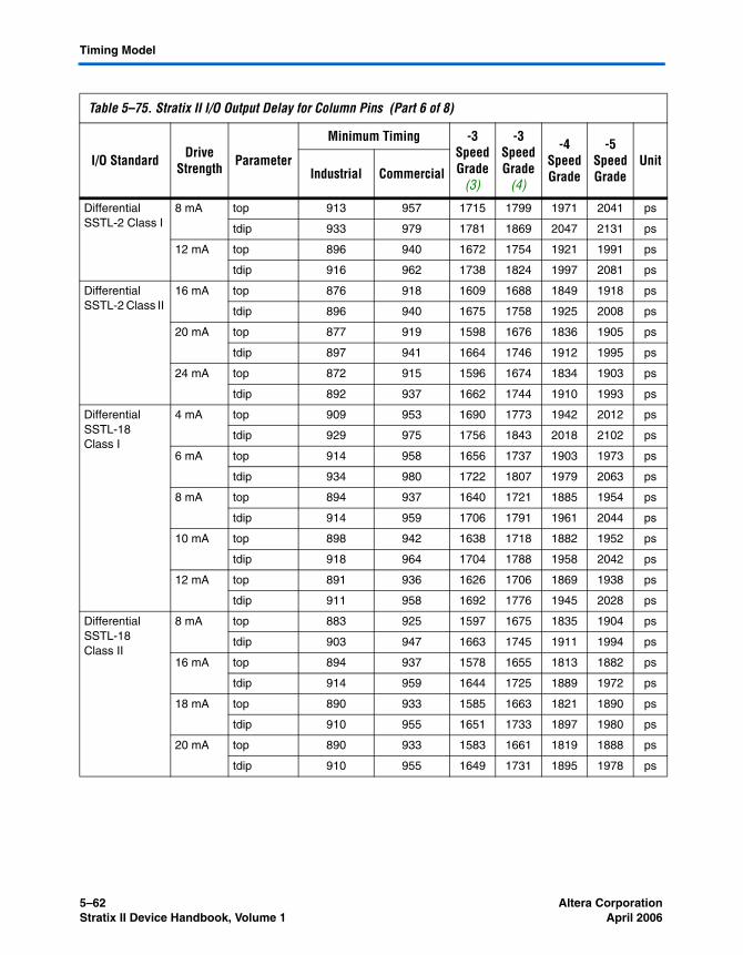
5–62 Altera CorporationStratix II Device Handbook, Volume 1 April 2006
Timing Model
Differential SSTL-2 Class I
8 mA top 913 957 1715 1799 1971 2041 ps
tdip 933 979 1781 1869 2047 2131 ps
12 mA top 896 940 1672 1754 1921 1991 ps
tdip 916 962 1738 1824 1997 2081 ps
Differential SSTL-2 Class II
16 mA top 876 918 1609 1688 1849 1918 ps
tdip 896 940 1675 1758 1925 2008 ps
20 mA top 877 919 1598 1676 1836 1905 ps
tdip 897 941 1664 1746 1912 1995 ps
24 mA top 872 915 1596 1674 1834 1903 ps
tdip 892 937 1662 1744 1910 1993 ps
Differential SSTL-18 Class I
4 mA top 909 953 1690 1773 1942 2012 ps
tdip 929 975 1756 1843 2018 2102 ps
6 mA top 914 958 1656 1737 1903 1973 ps
tdip 934 980 1722 1807 1979 2063 ps
8 mA top 894 937 1640 1721 1885 1954 ps
tdip 914 959 1706 1791 1961 2044 ps
10 mA top 898 942 1638 1718 1882 1952 ps
tdip 918 964 1704 1788 1958 2042 ps
12 mA top 891 936 1626 1706 1869 1938 ps
tdip 911 958 1692 1776 1945 2028 ps
Differential SSTL-18 Class II
8 mA top 883 925 1597 1675 1835 1904 ps
tdip 903 947 1663 1745 1911 1994 ps
16 mA top 894 937 1578 1655 1813 1882 ps
tdip 914 959 1644 1725 1889 1972 ps
18 mA top 890 933 1585 1663 1821 1890 ps
tdip 910 955 1651 1733 1897 1980 ps
20 mA top 890 933 1583 1661 1819 1888 ps
tdip 910 955 1649 1731 1895 1978 ps
Table 5–75. Stratix II I/O Output Delay for Column Pins (Part 6 of 8)
I/O Standard Drive Strength Parameter
Minimum Timing -3 Speed Grade
(3)
-3 Speed Grade
(4)
-4 Speed Grade
-5 Speed Grade
Unit Industrial Commercial
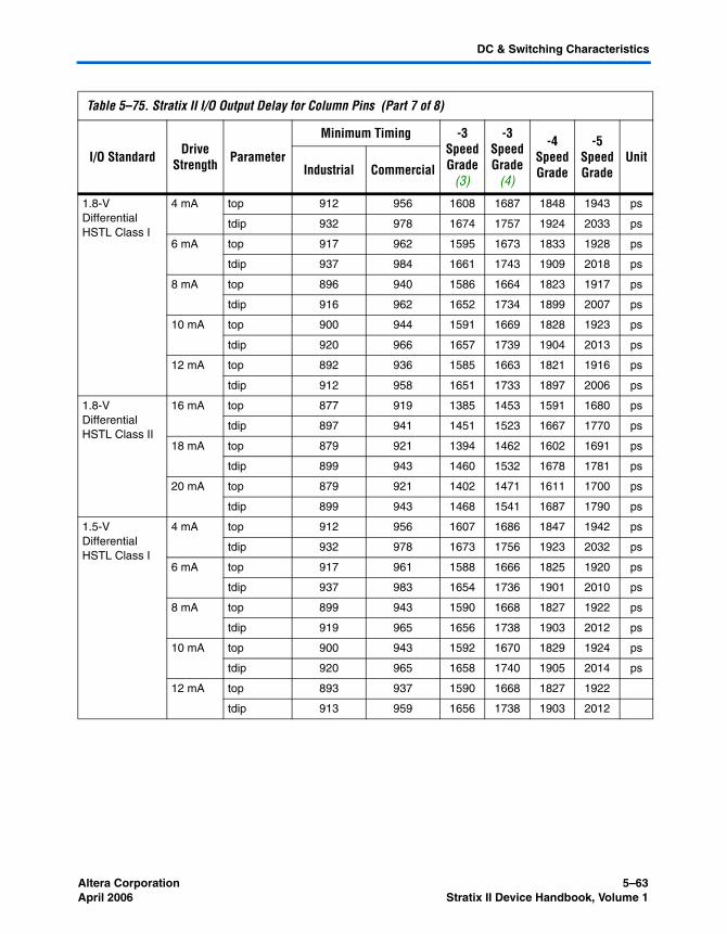
Altera Corporation 5–63April 2006 Stratix II Device Handbook, Volume 1
DC & Switching Characteristics
1.8-V Differential HSTL Class I
4 mA top 912 956 1608 1687 1848 1943 ps
tdip 932 978 1674 1757 1924 2033 ps
6 mA top 917 962 1595 1673 1833 1928 ps
tdip 937 984 1661 1743 1909 2018 ps
8 mA top 896 940 1586 1664 1823 1917 ps
tdip 916 962 1652 1734 1899 2007 ps
10 mA top 900 944 1591 1669 1828 1923 ps
tdip 920 966 1657 1739 1904 2013 ps
12 mA top 892 936 1585 1663 1821 1916 ps
tdip 912 958 1651 1733 1897 2006 ps
1.8-V Differential HSTL Class II
16 mA top 877 919 1385 1453 1591 1680 ps
tdip 897 941 1451 1523 1667 1770 ps
18 mA top 879 921 1394 1462 1602 1691 ps
tdip 899 943 1460 1532 1678 1781 ps
20 mA top 879 921 1402 1471 1611 1700 ps
tdip 899 943 1468 1541 1687 1790 ps
1.5-V Differential HSTL Class I
4 mA top 912 956 1607 1686 1847 1942 ps
tdip 932 978 1673 1756 1923 2032 ps
6 mA top 917 961 1588 1666 1825 1920 ps
tdip 937 983 1654 1736 1901 2010 ps
8 mA top 899 943 1590 1668 1827 1922 ps
tdip 919 965 1656 1738 1903 2012 ps
10 mA top 900 943 1592 1670 1829 1924 ps
tdip 920 965 1658 1740 1905 2014 ps
12 mA top 893 937 1590 1668 1827 1922
tdip 913 959 1656 1738 1903 2012
Table 5–75. Stratix II I/O Output Delay for Column Pins (Part 7 of 8)
I/O Standard Drive Strength Parameter
Minimum Timing -3 Speed Grade
(3)
-3 Speed Grade
(4)
-4 Speed Grade
-5 Speed Grade
Unit Industrial Commercial
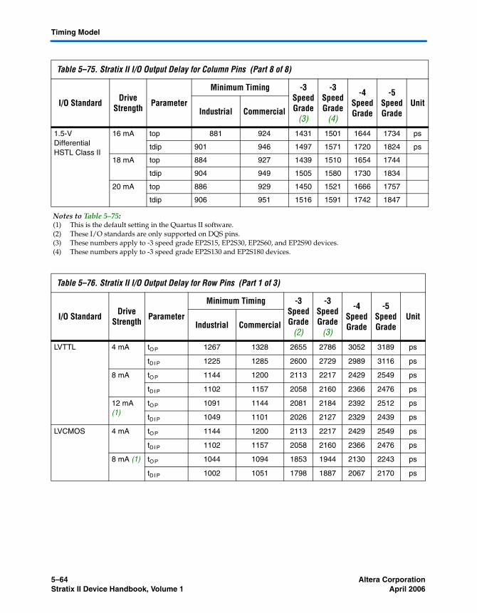
5–64 Altera CorporationStratix II Device Handbook, Volume 1 April 2006
Timing Model
1.5-V Differential HSTL Class II
16 mA top 881 924 1431 1501 1644 1734 ps
tdip 901 946 1497 1571 1720 1824 ps
18 mA top 884 927 1439 1510 1654 1744
tdip 904 949 1505 1580 1730 1834
20 mA top 886 929 1450 1521 1666 1757
tdip 906 951 1516 1591 1742 1847
Notes to Table 5–75:(1) This is the default setting in the Quartus II software.(2) These I/O standards are only supported on DQS pins.(3) These numbers apply to -3 speed grade EP2S15, EP2S30, EP2S60, and EP2S90 devices.(4) These numbers apply to -3 speed grade EP2S130 and EP2S180 devices.
Table 5–76. Stratix II I/O Output Delay for Row Pins (Part 1 of 3)
I/O Standard Drive Strength Parameter
Minimum Timing -3 Speed Grade
(2)
-3 Speed Grade
(3)
-4 Speed Grade
-5 Speed Grade
Unit Industrial Commercial
LVTTL 4 mA tO P 1267 1328 2655 2786 3052 3189 ps
tD I P 1225 1285 2600 2729 2989 3116 ps
8 mA tO P 1144 1200 2113 2217 2429 2549 ps
tD I P 1102 1157 2058 2160 2366 2476 ps
12 mA (1)
tO P 1091 1144 2081 2184 2392 2512 ps
tD I P 1049 1101 2026 2127 2329 2439 ps
LVCMOS 4 mA tO P 1144 1200 2113 2217 2429 2549 ps
tD I P 1102 1157 2058 2160 2366 2476 ps
8 mA (1) tO P 1044 1094 1853 1944 2130 2243 ps
tD I P 1002 1051 1798 1887 2067 2170 ps
Table 5–75. Stratix II I/O Output Delay for Column Pins (Part 8 of 8)
I/O Standard Drive Strength Parameter
Minimum Timing -3 Speed Grade
(3)
-3 Speed Grade
(4)
-4 Speed Grade
-5 Speed Grade
Unit Industrial Commercial
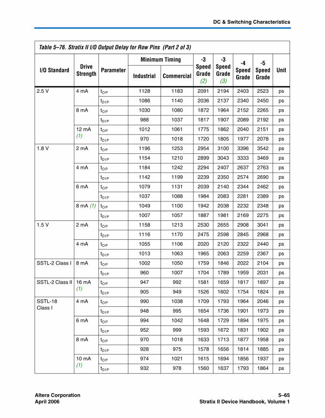
Altera Corporation 5–65April 2006 Stratix II Device Handbook, Volume 1
DC & Switching Characteristics
2.5 V 4 mA tO P 1128 1183 2091 2194 2403 2523 ps
tD I P 1086 1140 2036 2137 2340 2450 ps
8 mA tO P 1030 1080 1872 1964 2152 2265 ps
tD I P 988 1037 1817 1907 2089 2192 ps
12 mA (1)
tO P 1012 1061 1775 1862 2040 2151 ps
tD I P 970 1018 1720 1805 1977 2078 ps
1.8 V 2 mA tO P 1196 1253 2954 3100 3396 3542 ps
tD I P 1154 1210 2899 3043 3333 3469 ps
4 mA tO P 1184 1242 2294 2407 2637 2763 ps
tD I P 1142 1199 2239 2350 2574 2690 ps
6 mA tO P 1079 1131 2039 2140 2344 2462 ps
tD I P 1037 1088 1984 2083 2281 2389 ps
8 mA (1) tO P 1049 1100 1942 2038 2232 2348 ps
tD I P 1007 1057 1887 1981 2169 2275 ps
1.5 V 2 mA tO P 1158 1213 2530 2655 2908 3041 ps
tD I P 1116 1170 2475 2598 2845 2968 ps
4 mA tO P 1055 1106 2020 2120 2322 2440 ps
tD I P 1013 1063 1965 2063 2259 2367 ps
SSTL-2 Class I 8 mA tO P 1002 1050 1759 1846 2022 2104 ps
tD I P 960 1007 1704 1789 1959 2031 ps
SSTL-2 Class II 16 mA (1)
tO P 947 992 1581 1659 1817 1897 ps
tD I P 905 949 1526 1602 1754 1824 ps
SSTL-18 Class I
4 mA tO P 990 1038 1709 1793 1964 2046 ps
tD I P 948 995 1654 1736 1901 1973 ps
6 mA tO P 994 1042 1648 1729 1894 1975 ps
tD I P 952 999 1593 1672 1831 1902 ps
8 mA tO P 970 1018 1633 1713 1877 1958 ps
tD I P 928 975 1578 1656 1814 1885 ps
10 mA (1)
tO P 974 1021 1615 1694 1856 1937 ps
tD I P 932 978 1560 1637 1793 1864 ps
Table 5–76. Stratix II I/O Output Delay for Row Pins (Part 2 of 3)
I/O Standard Drive Strength Parameter
Minimum Timing -3 Speed Grade
(2)
-3 Speed Grade
(3)
-4 Speed Grade
-5 Speed Grade
Unit Industrial Commercial
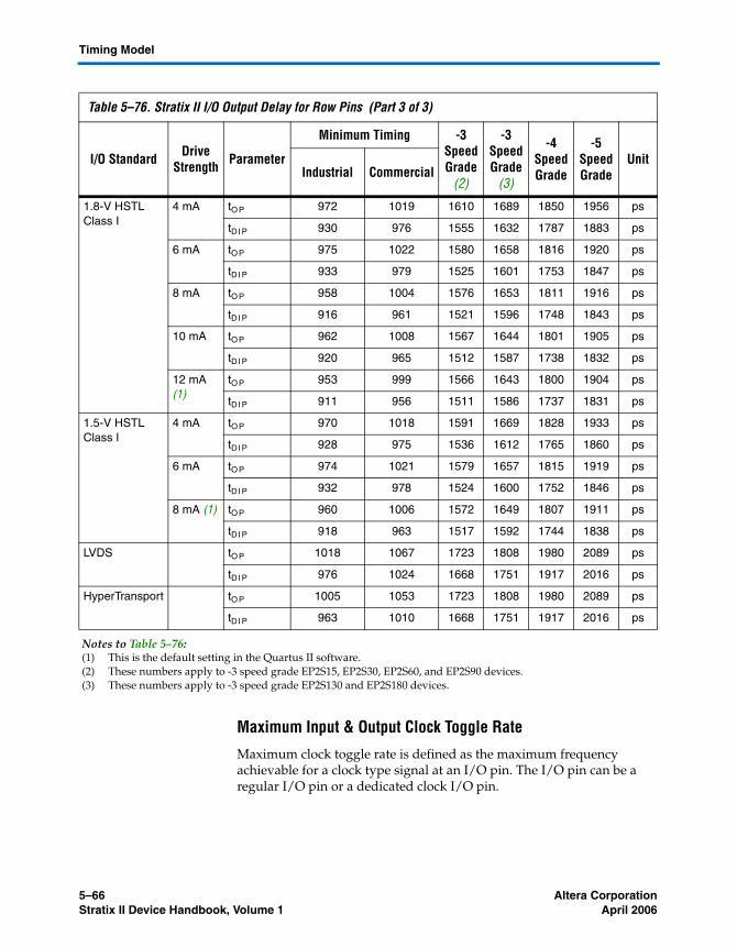
5–66 Altera CorporationStratix II Device Handbook, Volume 1 April 2006
Timing Model
Maximum Input & Output Clock Toggle Rate
Maximum clock toggle rate is defined as the maximum frequency achievable for a clock type signal at an I/O pin. The I/O pin can be a regular I/O pin or a dedicated clock I/O pin.
1.8-V HSTL Class I
4 mA tO P 972 1019 1610 1689 1850 1956 ps
tD I P 930 976 1555 1632 1787 1883 ps
6 mA tO P 975 1022 1580 1658 1816 1920 ps
tD I P 933 979 1525 1601 1753 1847 ps
8 mA tO P 958 1004 1576 1653 1811 1916 ps
tD I P 916 961 1521 1596 1748 1843 ps
10 mA tO P 962 1008 1567 1644 1801 1905 ps
tD I P 920 965 1512 1587 1738 1832 ps
12 mA (1)
tO P 953 999 1566 1643 1800 1904 ps
tD I P 911 956 1511 1586 1737 1831 ps
1.5-V HSTL Class I
4 mA tO P 970 1018 1591 1669 1828 1933 ps
tD I P 928 975 1536 1612 1765 1860 ps
6 mA tO P 974 1021 1579 1657 1815 1919 ps
tD I P 932 978 1524 1600 1752 1846 ps
8 mA (1) tO P 960 1006 1572 1649 1807 1911 ps
tD I P 918 963 1517 1592 1744 1838 ps
LVDS tO P 1018 1067 1723 1808 1980 2089 ps
tD I P 976 1024 1668 1751 1917 2016 ps
HyperTransport tO P 1005 1053 1723 1808 1980 2089 ps
tD I P 963 1010 1668 1751 1917 2016 ps
Notes to Table 5–76:(1) This is the default setting in the Quartus II software.(2) These numbers apply to -3 speed grade EP2S15, EP2S30, EP2S60, and EP2S90 devices.(3) These numbers apply to -3 speed grade EP2S130 and EP2S180 devices.
Table 5–76. Stratix II I/O Output Delay for Row Pins (Part 3 of 3)
I/O Standard Drive Strength Parameter
Minimum Timing -3 Speed Grade
(2)
-3 Speed Grade
(3)
-4 Speed Grade
-5 Speed Grade
Unit Industrial Commercial
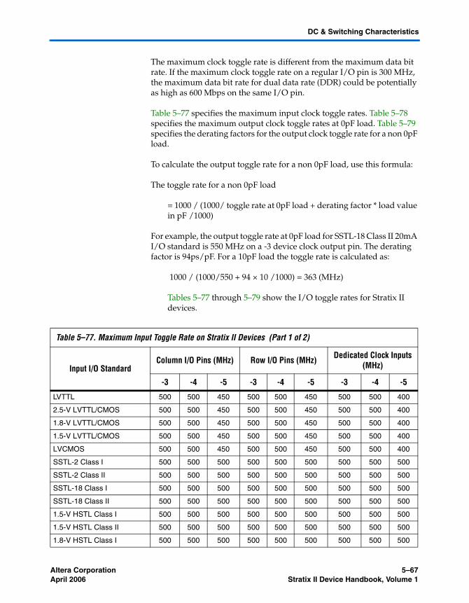
Altera Corporation 5–67April 2006 Stratix II Device Handbook, Volume 1
DC & Switching Characteristics
The maximum clock toggle rate is different from the maximum data bit rate. If the maximum clock toggle rate on a regular I/O pin is 300 MHz, the maximum data bit rate for dual data rate (DDR) could be potentially as high as 600 Mbps on the same I/O pin.
Table 5–77 specifies the maximum input clock toggle rates. Table 5–78 specifies the maximum output clock toggle rates at 0pF load. Table 5–79 specifies the derating factors for the output clock toggle rate for a non 0pF load.
To calculate the output toggle rate for a non 0pF load, use this formula:
The toggle rate for a non 0pF load
= 1000 / (1000/ toggle rate at 0pF load + derating factor * load value in pF /1000)
For example, the output toggle rate at 0pF load for SSTL-18 Class II 20mA I/O standard is 550 MHz on a -3 device clock output pin. The derating factor is 94ps/pF. For a 10pF load the toggle rate is calculated as:
1000 / (1000/550 + 94 × 10 /1000) = 363 (MHz)
Tables 5–77 through 5–79 show the I/O toggle rates for Stratix II devices.
Table 5–77. Maximum Input Toggle Rate on Stratix II Devices (Part 1 of 2)
Input I/O StandardColumn I/O Pins (MHz) Row I/O Pins (MHz) Dedicated Clock Inputs
(MHz)
-3 -4 -5 -3 -4 -5 -3 -4 -5
LVTTL 500 500 450 500 500 450 500 500 400
2.5-V LVTTL/CMOS 500 500 450 500 500 450 500 500 400
1.8-V LVTTL/CMOS 500 500 450 500 500 450 500 500 400
1.5-V LVTTL/CMOS 500 500 450 500 500 450 500 500 400
LVCMOS 500 500 450 500 500 450 500 500 400
SSTL-2 Class I 500 500 500 500 500 500 500 500 500
SSTL-2 Class II 500 500 500 500 500 500 500 500 500
SSTL-18 Class I 500 500 500 500 500 500 500 500 500
SSTL-18 Class II 500 500 500 500 500 500 500 500 500
1.5-V HSTL Class I 500 500 500 500 500 500 500 500 500
1.5-V HSTL Class II 500 500 500 500 500 500 500 500 500
1.8-V HSTL Class I 500 500 500 500 500 500 500 500 500
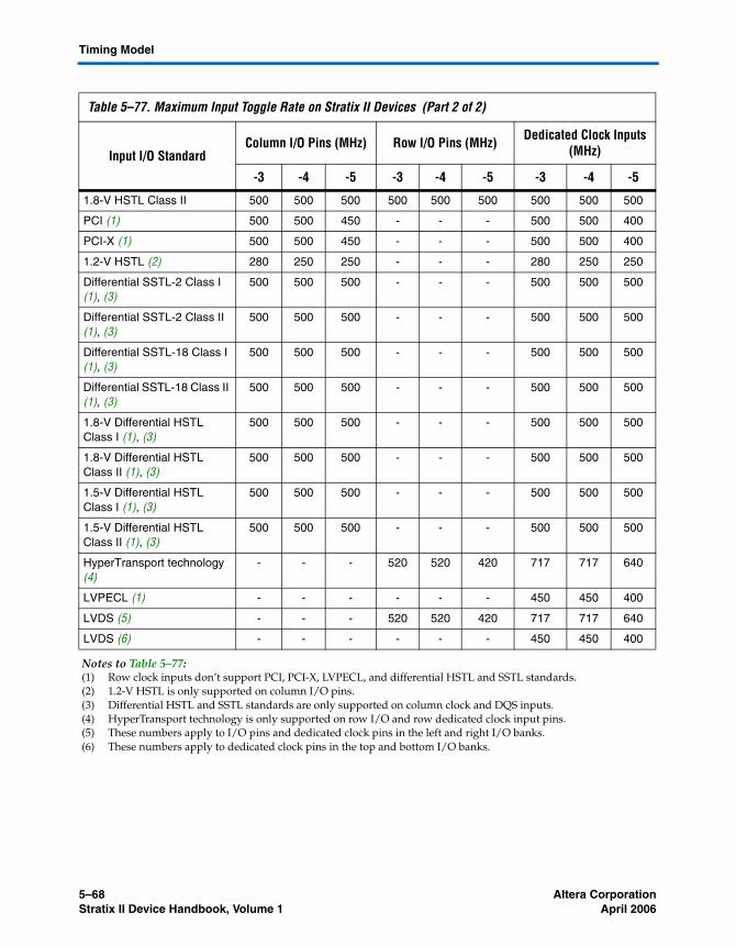
5–68 Altera CorporationStratix II Device Handbook, Volume 1 April 2006
Timing Model
1.8-V HSTL Class II 500 500 500 500 500 500 500 500 500
PCI (1) 500 500 450 - - - 500 500 400
PCI-X (1) 500 500 450 - - - 500 500 400
1.2-V HSTL (2) 280 250 250 - - - 280 250 250
Differential SSTL-2 Class I (1), (3)
500 500 500 - - - 500 500 500
Differential SSTL-2 Class II (1), (3)
500 500 500 - - - 500 500 500
Differential SSTL-18 Class I (1), (3)
500 500 500 - - - 500 500 500
Differential SSTL-18 Class II (1), (3)
500 500 500 - - - 500 500 500
1.8-V Differential HSTL Class I (1), (3)
500 500 500 - - - 500 500 500
1.8-V Differential HSTL Class II (1), (3)
500 500 500 - - - 500 500 500
1.5-V Differential HSTL Class I (1), (3)
500 500 500 - - - 500 500 500
1.5-V Differential HSTL Class II (1), (3)
500 500 500 - - - 500 500 500
HyperTransport technology (4)
- - - 520 520 420 717 717 640
LVPECL (1) - - - - - - 450 450 400
LVDS (5) - - - 520 520 420 717 717 640
LVDS (6) - - - - - - 450 450 400
Notes to Table 5–77:(1) Row clock inputs don’t support PCI, PCI-X, LVPECL, and differential HSTL and SSTL standards.(2) 1.2-V HSTL is only supported on column I/O pins.(3) Differential HSTL and SSTL standards are only supported on column clock and DQS inputs.(4) HyperTransport technology is only supported on row I/O and row dedicated clock input pins.(5) These numbers apply to I/O pins and dedicated clock pins in the left and right I/O banks.(6) These numbers apply to dedicated clock pins in the top and bottom I/O banks.
Table 5–77. Maximum Input Toggle Rate on Stratix II Devices (Part 2 of 2)
Input I/O StandardColumn I/O Pins (MHz) Row I/O Pins (MHz) Dedicated Clock Inputs
(MHz)
-3 -4 -5 -3 -4 -5 -3 -4 -5
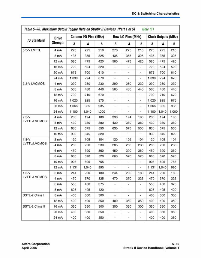
Altera Corporation 5–69April 2006 Stratix II Device Handbook, Volume 1
DC & Switching Characteristics
Table 5–78. Maximum Output Toggle Rate on Stratix II Devices (Part 1 of 5) Note (1)
I/O Standard Drive Strength
Column I/O Pins (MHz) Row I/O Pins (MHz) Clock Outputs (MHz)
-3 -4 -5 -3 -4 -5 -3 -4 -5
3.3-V LVTTL 4 mA 270 225 210 270 225 210 270 225 210
8 mA 435 355 325 435 355 325 435 355 325
12 mA 580 475 420 580 475 420 580 475 420
16 mA 720 594 520 - - - 720 594 520
20 mA 875 700 610 - - - 875 700 610
24 mA 1,030 794 670 - - - 1,030 794 670
3.3-V LVCMOS 4 mA 290 250 230 290 250 230 290 250 230
8 mA 565 480 440 565 480 440 565 480 440
12 mA 790 710 670 - - - 790 710 670
16 mA 1,020 925 875 - - - 1,020 925 875
20 mA 1,066 985 935 - - - 1,066 985 935
24 mA 1,100 1,040 1,000 - - - 1,100 1,040 1,000
2.5-V LVTTL/LVCMOS
4 mA 230 194 180 230 194 180 230 194 180
8 mA 430 380 380 430 380 380 430 380 380
12 mA 630 575 550 630 575 550 630 575 550
16 mA 930 845 820 - - - 930 845 820
1.8-V LVTTL/LVCMOS
2 mA 120 109 104 120 109 104 120 109 104
4 mA 285 250 230 285 250 230 285 250 230
6 mA 450 390 360 450 390 360 450 390 360
8 mA 660 570 520 660 570 520 660 570 520
10 mA 905 805 755 - - - 905 805 755
12 mA 1,131 1,040 990 - - - 1,131 1,040 990
1.5-V LVTTL/LVCMOS
2 mA 244 200 180 244 200 180 244 200 180
4 mA 470 370 325 470 370 325 470 370 325
6 mA 550 430 375 - - - 550 430 375
8 mA 625 495 420 - - - 625 495 420
SSTL-2 Class I 8 mA 400 300 300 - - - 400 300 300
12 mA 400 400 350 400 350 350 400 400 350
SSTL-2 Class II 16 mA 350 350 300 350 350 300 350 350 300
20 mA 400 350 350 - - - 400 350 350
24 mA 400 400 350 - - - 400 400 350
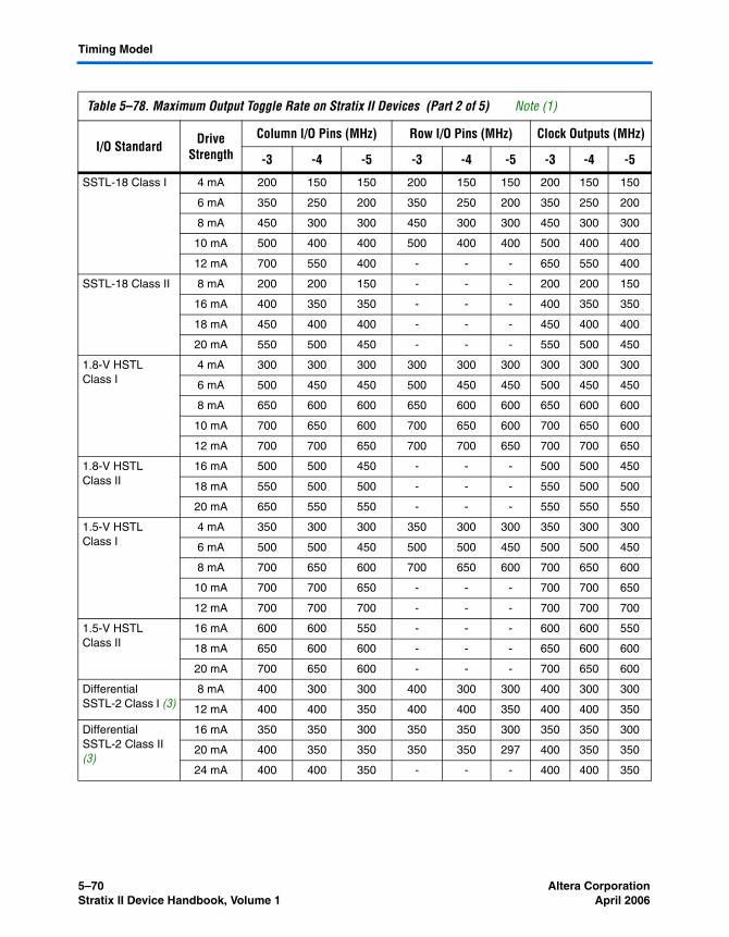
5–70 Altera CorporationStratix II Device Handbook, Volume 1 April 2006
Timing Model
SSTL-18 Class I 4 mA 200 150 150 200 150 150 200 150 150
6 mA 350 250 200 350 250 200 350 250 200
8 mA 450 300 300 450 300 300 450 300 300
10 mA 500 400 400 500 400 400 500 400 400
12 mA 700 550 400 - - - 650 550 400
SSTL-18 Class II 8 mA 200 200 150 - - - 200 200 150
16 mA 400 350 350 - - - 400 350 350
18 mA 450 400 400 - - - 450 400 400
20 mA 550 500 450 - - - 550 500 450
1.8-V HSTL Class I
4 mA 300 300 300 300 300 300 300 300 300
6 mA 500 450 450 500 450 450 500 450 450
8 mA 650 600 600 650 600 600 650 600 600
10 mA 700 650 600 700 650 600 700 650 600
12 mA 700 700 650 700 700 650 700 700 650
1.8-V HSTL Class II
16 mA 500 500 450 - - - 500 500 450
18 mA 550 500 500 - - - 550 500 500
20 mA 650 550 550 - - - 550 550 550
1.5-V HSTL Class I
4 mA 350 300 300 350 300 300 350 300 300
6 mA 500 500 450 500 500 450 500 500 450
8 mA 700 650 600 700 650 600 700 650 600
10 mA 700 700 650 - - - 700 700 650
12 mA 700 700 700 - - - 700 700 700
1.5-V HSTL Class II
16 mA 600 600 550 - - - 600 600 550
18 mA 650 600 600 - - - 650 600 600
20 mA 700 650 600 - - - 700 650 600
Differential SSTL-2 Class I (3)
8 mA 400 300 300 400 300 300 400 300 300
12 mA 400 400 350 400 400 350 400 400 350
Differential SSTL-2 Class II (3)
16 mA 350 350 300 350 350 300 350 350 300
20 mA 400 350 350 350 350 297 400 350 350
24 mA 400 400 350 - - - 400 400 350
Table 5–78. Maximum Output Toggle Rate on Stratix II Devices (Part 2 of 5) Note (1)
I/O Standard Drive Strength
Column I/O Pins (MHz) Row I/O Pins (MHz) Clock Outputs (MHz)
-3 -4 -5 -3 -4 -5 -3 -4 -5
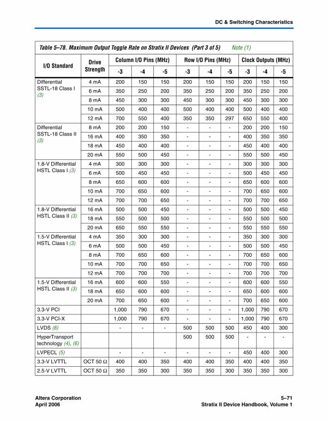
Altera Corporation 5–71April 2006 Stratix II Device Handbook, Volume 1
DC & Switching Characteristics
Differential SSTL-18 Class I (3)
4 mA 200 150 150 200 150 150 200 150 150
6 mA 350 250 200 350 250 200 350 250 200
8 mA 450 300 300 450 300 300 450 300 300
10 mA 500 400 400 500 400 400 500 400 400
12 mA 700 550 400 350 350 297 650 550 400
Differential SSTL-18 Class II (3)
8 mA 200 200 150 - - - 200 200 150
16 mA 400 350 350 - - - 400 350 350
18 mA 450 400 400 - - - 450 400 400
20 mA 550 500 450 - - - 550 500 450
1.8-V Differential HSTL Class I (3)
4 mA 300 300 300 - - - 300 300 300
6 mA 500 450 450 - - - 500 450 450
8 mA 650 600 600 - - - 650 600 600
10 mA 700 650 600 - - - 700 650 600
12 mA 700 700 650 - - - 700 700 650
1.8-V Differential HSTL Class II (3)
16 mA 500 500 450 - - - 500 500 450
18 mA 550 500 500 - - - 550 500 500
20 mA 650 550 550 - - - 550 550 550
1.5-V Differential HSTL Class I (3)
4 mA 350 300 300 - - - 350 300 300
6 mA 500 500 450 - - - 500 500 450
8 mA 700 650 600 - - - 700 650 600
10 mA 700 700 650 - - - 700 700 650
12 mA 700 700 700 - - - 700 700 700
1.5-V Differential HSTL Class II (3)
16 mA 600 600 550 - - - 600 600 550
18 mA 650 600 600 - - - 650 600 600
20 mA 700 650 600 - - - 700 650 600
3.3-V PCI 1,000 790 670 - - - 1,000 790 670
3.3-V PCI-X 1,000 790 670 - - - 1,000 790 670
LVDS (6) - - - 500 500 500 450 400 300
HyperTransport technology (4), (6)
500 500 500 - - -
LVPECL (5) - - - - - - 450 400 300
3.3-V LVTTL OCT 50 Ω 400 400 350 400 400 350 400 400 350
2.5-V LVTTL OCT 50 Ω 350 350 300 350 350 300 350 350 300
Table 5–78. Maximum Output Toggle Rate on Stratix II Devices (Part 3 of 5) Note (1)
I/O Standard Drive Strength
Column I/O Pins (MHz) Row I/O Pins (MHz) Clock Outputs (MHz)
-3 -4 -5 -3 -4 -5 -3 -4 -5
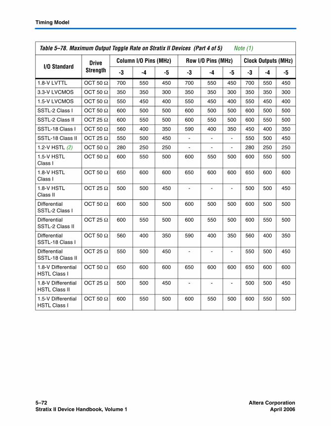
5–72 Altera CorporationStratix II Device Handbook, Volume 1 April 2006
Timing Model
1.8-V LVTTL OCT 50 Ω 700 550 450 700 550 450 700 550 450
3.3-V LVCMOS OCT 50 Ω 350 350 300 350 350 300 350 350 300
1.5-V LVCMOS OCT 50 Ω 550 450 400 550 450 400 550 450 400
SSTL-2 Class I OCT 50 Ω 600 500 500 600 500 500 600 500 500
SSTL-2 Class II OCT 25 Ω 600 550 500 600 550 500 600 550 500
SSTL-18 Class I OCT 50 Ω 560 400 350 590 400 350 450 400 350
SSTL-18 Class II OCT 25 Ω 550 500 450 - - - 550 500 450
1.2-V HSTL (2) OCT 50 Ω 280 250 250 - - - 280 250 250
1.5-V HSTL Class I
OCT 50 Ω 600 550 500 600 550 500 600 550 500
1.8-V HSTL Class I
OCT 50 Ω 650 600 600 650 600 600 650 600 600
1.8-V HSTL Class II
OCT 25 Ω 500 500 450 - - - 500 500 450
Differential SSTL-2 Class I
OCT 50 Ω 600 500 500 600 500 500 600 500 500
Differential SSTL-2 Class II
OCT 25 Ω 600 550 500 600 550 500 600 550 500
Differential SSTL-18 Class I
OCT 50 Ω 560 400 350 590 400 350 560 400 350
Differential SSTL-18 Class II
OCT 25 Ω 550 500 450 - - - 550 500 450
1.8-V Differential HSTL Class I
OCT 50 Ω 650 600 600 650 600 600 650 600 600
1.8-V Differential HSTL Class II
OCT 25 Ω 500 500 450 - - - 500 500 450
1.5-V Differential HSTL Class I
OCT 50 Ω 600 550 500 600 550 500 600 550 500
Table 5–78. Maximum Output Toggle Rate on Stratix II Devices (Part 4 of 5) Note (1)
I/O Standard Drive Strength
Column I/O Pins (MHz) Row I/O Pins (MHz) Clock Outputs (MHz)
-3 -4 -5 -3 -4 -5 -3 -4 -5
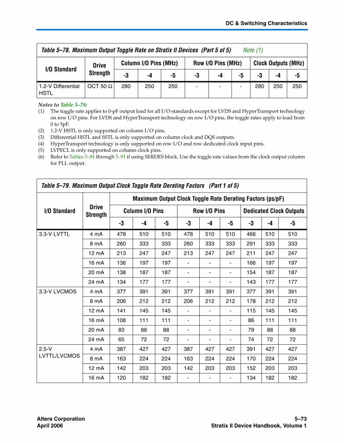
Altera Corporation 5–73April 2006 Stratix II Device Handbook, Volume 1
DC & Switching Characteristics
1.2-V Differential HSTL
OCT 50 Ω 280 250 250 - - - 280 250 250
Notes to Table 5–78:(1) The toggle rate applies to 0-pF output load for all I/O standards except for LVDS and HyperTransport technology
on row I/O pins. For LVDS and HyperTransport technology on row I/O pins, the toggle rates apply to load from 0 to 5pF.
(2) 1.2-V HSTL is only supported on column I/O pins.(3) Differential HSTL and SSTL is only supported on column clock and DQS outputs.(4) HyperTransport technology is only supported on row I/O and row dedicated clock input pins.(5) LVPECL is only supported on column clock pins.(6) Refer to Tables 5–81 through 5–91 if using SERDES block. Use the toggle rate values from the clock output column
for PLL output.
Table 5–79. Maximum Output Clock Toggle Rate Derating Factors (Part 1 of 5)
I/O Standard Drive Strength
Maximum Output Clock Toggle Rate Derating Factors (ps/pF)
Column I/O Pins Row I/O Pins Dedicated Clock Outputs
-3 -4 -5 -3 -4 -5 -3 -4 -5
3.3-V LVTTL 4 mA 478 510 510 478 510 510 466 510 510
8 mA 260 333 333 260 333 333 291 333 333
12 mA 213 247 247 213 247 247 211 247 247
16 mA 136 197 197 - - - 166 197 197
20 mA 138 187 187 - - - 154 187 187
24 mA 134 177 177 - - - 143 177 177
3.3-V LVCMOS 4 mA 377 391 391 377 391 391 377 391 391
8 mA 206 212 212 206 212 212 178 212 212
12 mA 141 145 145 - - - 115 145 145
16 mA 108 111 111 - - - 86 111 111
20 mA 83 88 88 - - - 79 88 88
24 mA 65 72 72 - - - 74 72 72
2.5-V LVTTL/LVCMOS
4 mA 387 427 427 387 427 427 391 427 427
8 mA 163 224 224 163 224 224 170 224 224
12 mA 142 203 203 142 203 203 152 203 203
16 mA 120 182 182 - - - 134 182 182
Table 5–78. Maximum Output Toggle Rate on Stratix II Devices (Part 5 of 5) Note (1)
I/O Standard Drive Strength
Column I/O Pins (MHz) Row I/O Pins (MHz) Clock Outputs (MHz)
-3 -4 -5 -3 -4 -5 -3 -4 -5
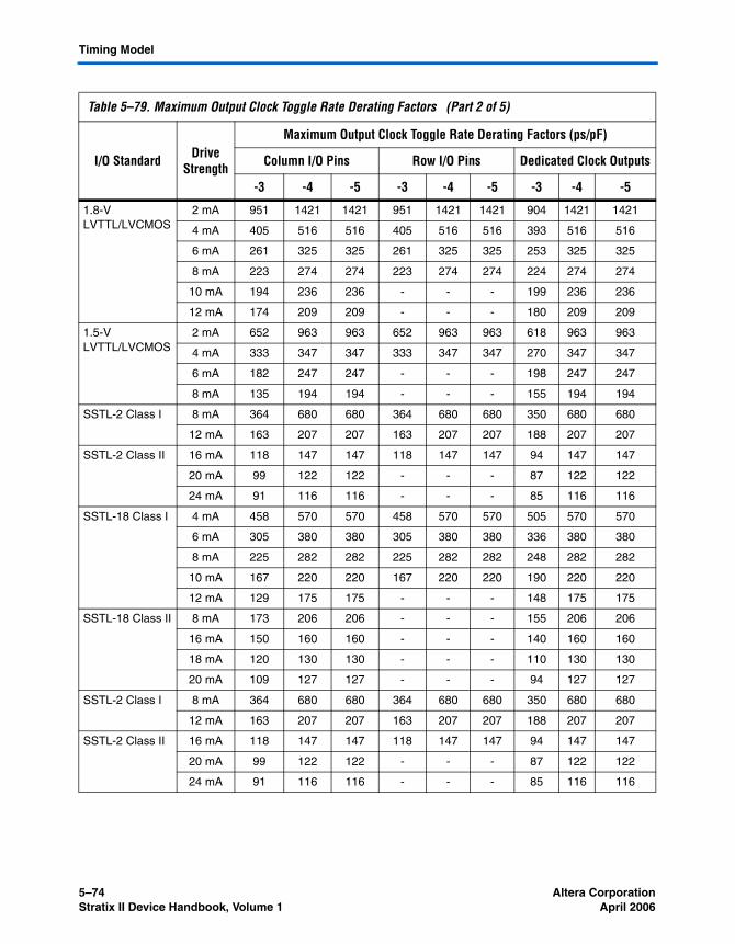
5–74 Altera CorporationStratix II Device Handbook, Volume 1 April 2006
Timing Model
1.8-V LVTTL/LVCMOS
2 mA 951 1421 1421 951 1421 1421 904 1421 1421
4 mA 405 516 516 405 516 516 393 516 516
6 mA 261 325 325 261 325 325 253 325 325
8 mA 223 274 274 223 274 274 224 274 274
10 mA 194 236 236 - - - 199 236 236
12 mA 174 209 209 - - - 180 209 209
1.5-V LVTTL/LVCMOS
2 mA 652 963 963 652 963 963 618 963 963
4 mA 333 347 347 333 347 347 270 347 347
6 mA 182 247 247 - - - 198 247 247
8 mA 135 194 194 - - - 155 194 194
SSTL-2 Class I 8 mA 364 680 680 364 680 680 350 680 680
12 mA 163 207 207 163 207 207 188 207 207
SSTL-2 Class II 16 mA 118 147 147 118 147 147 94 147 147
20 mA 99 122 122 - - - 87 122 122
24 mA 91 116 116 - - - 85 116 116
SSTL-18 Class I 4 mA 458 570 570 458 570 570 505 570 570
6 mA 305 380 380 305 380 380 336 380 380
8 mA 225 282 282 225 282 282 248 282 282
10 mA 167 220 220 167 220 220 190 220 220
12 mA 129 175 175 - - - 148 175 175
SSTL-18 Class II 8 mA 173 206 206 - - - 155 206 206
16 mA 150 160 160 - - - 140 160 160
18 mA 120 130 130 - - - 110 130 130
20 mA 109 127 127 - - - 94 127 127
SSTL-2 Class I 8 mA 364 680 680 364 680 680 350 680 680
12 mA 163 207 207 163 207 207 188 207 207
SSTL-2 Class II 16 mA 118 147 147 118 147 147 94 147 147
20 mA 99 122 122 - - - 87 122 122
24 mA 91 116 116 - - - 85 116 116
Table 5–79. Maximum Output Clock Toggle Rate Derating Factors (Part 2 of 5)
I/O Standard Drive Strength
Maximum Output Clock Toggle Rate Derating Factors (ps/pF)
Column I/O Pins Row I/O Pins Dedicated Clock Outputs
-3 -4 -5 -3 -4 -5 -3 -4 -5
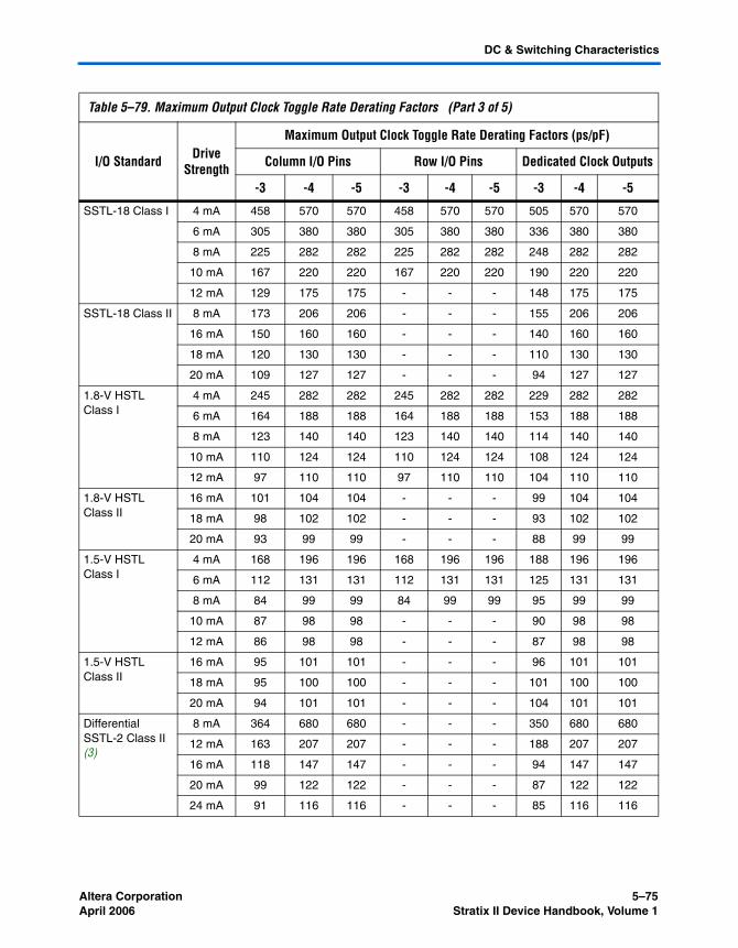
Altera Corporation 5–75April 2006 Stratix II Device Handbook, Volume 1
DC & Switching Characteristics
SSTL-18 Class I 4 mA 458 570 570 458 570 570 505 570 570
6 mA 305 380 380 305 380 380 336 380 380
8 mA 225 282 282 225 282 282 248 282 282
10 mA 167 220 220 167 220 220 190 220 220
12 mA 129 175 175 - - - 148 175 175
SSTL-18 Class II 8 mA 173 206 206 - - - 155 206 206
16 mA 150 160 160 - - - 140 160 160
18 mA 120 130 130 - - - 110 130 130
20 mA 109 127 127 - - - 94 127 127
1.8-V HSTL Class I
4 mA 245 282 282 245 282 282 229 282 282
6 mA 164 188 188 164 188 188 153 188 188
8 mA 123 140 140 123 140 140 114 140 140
10 mA 110 124 124 110 124 124 108 124 124
12 mA 97 110 110 97 110 110 104 110 110
1.8-V HSTL Class II
16 mA 101 104 104 - - - 99 104 104
18 mA 98 102 102 - - - 93 102 102
20 mA 93 99 99 - - - 88 99 99
1.5-V HSTL Class I
4 mA 168 196 196 168 196 196 188 196 196
6 mA 112 131 131 112 131 131 125 131 131
8 mA 84 99 99 84 99 99 95 99 99
10 mA 87 98 98 - - - 90 98 98
12 mA 86 98 98 - - - 87 98 98
1.5-V HSTL Class II
16 mA 95 101 101 - - - 96 101 101
18 mA 95 100 100 - - - 101 100 100
20 mA 94 101 101 - - - 104 101 101
Differential SSTL-2 Class II (3)
8 mA 364 680 680 - - - 350 680 680
12 mA 163 207 207 - - - 188 207 207
16 mA 118 147 147 - - - 94 147 147
20 mA 99 122 122 - - - 87 122 122
24 mA 91 116 116 - - - 85 116 116
Table 5–79. Maximum Output Clock Toggle Rate Derating Factors (Part 3 of 5)
I/O Standard Drive Strength
Maximum Output Clock Toggle Rate Derating Factors (ps/pF)
Column I/O Pins Row I/O Pins Dedicated Clock Outputs
-3 -4 -5 -3 -4 -5 -3 -4 -5
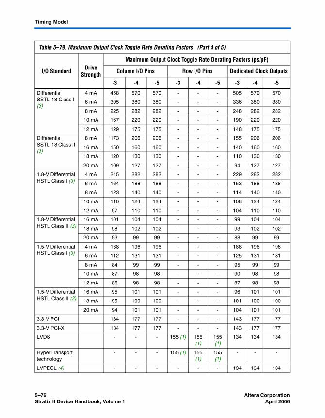
5–76 Altera CorporationStratix II Device Handbook, Volume 1 April 2006
Timing Model
Differential SSTL-18 Class I (3)
4 mA 458 570 570 - - - 505 570 570
6 mA 305 380 380 - - - 336 380 380
8 mA 225 282 282 - - - 248 282 282
10 mA 167 220 220 - - - 190 220 220
12 mA 129 175 175 - - - 148 175 175
Differential SSTL-18 Class II (3)
8 mA 173 206 206 - - - 155 206 206
16 mA 150 160 160 - - - 140 160 160
18 mA 120 130 130 - - - 110 130 130
20 mA 109 127 127 - - - 94 127 127
1.8-V Differential HSTL Class I (3)
4 mA 245 282 282 - - - 229 282 282
6 mA 164 188 188 - - - 153 188 188
8 mA 123 140 140 - - - 114 140 140
10 mA 110 124 124 - - - 108 124 124
12 mA 97 110 110 - - - 104 110 110
1.8-V Differential HSTL Class II (3)
16 mA 101 104 104 - - - 99 104 104
18 mA 98 102 102 - - - 93 102 102
20 mA 93 99 99 - - - 88 99 99
1.5-V Differential HSTL Class I (3)
4 mA 168 196 196 - - - 188 196 196
6 mA 112 131 131 - - - 125 131 131
8 mA 84 99 99 - - - 95 99 99
10 mA 87 98 98 - - - 90 98 98
12 mA 86 98 98 - - - 87 98 98
1.5-V Differential HSTL Class II (3)
16 mA 95 101 101 - - - 96 101 101
18 mA 95 100 100 - - - 101 100 100
20 mA 94 101 101 - - - 104 101 101
3.3-V PCI 134 177 177 - - - 143 177 177
3.3-V PCI-X 134 177 177 - - - 143 177 177
LVDS - - - 155 (1) 155 (1)
155 (1)
134 134 134
HyperTransport technology
- - - 155 (1) 155 (1)
155 (1)
- - -
LVPECL (4) - - - - - - 134 134 134
Table 5–79. Maximum Output Clock Toggle Rate Derating Factors (Part 4 of 5)
I/O Standard Drive Strength
Maximum Output Clock Toggle Rate Derating Factors (ps/pF)
Column I/O Pins Row I/O Pins Dedicated Clock Outputs
-3 -4 -5 -3 -4 -5 -3 -4 -5
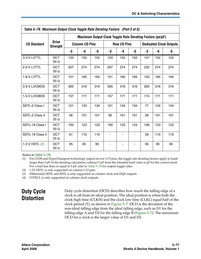
Altera Corporation 5–77April 2006 Stratix II Device Handbook, Volume 1
DC & Switching Characteristics
Duty Cycle Distortion
Duty cycle distortion (DCD) describes how much the falling edge of a clock is off from its ideal position. The ideal position is when both the clock high time (CLKH) and the clock low time (CLKL) equal half of the clock period (T), as shown in Figure 5–7. DCD is the deviation of the non-ideal falling edge from the ideal falling edge, such as D1 for the falling edge A and D2 for the falling edge B (Figure 5–7). The maximum DCD for a clock is the larger value of D1 and D2.
3.3-V LVTTL OCT 50 Ω
133 152 152 133 152 152 147 152 152
2.5-V LVTTL OCT 50 Ω
207 274 274 207 274 274 235 274 274
1.8-V LVTTL OCT 50 Ω
151 165 165 151 165 165 153 165 165
3.3-V LVCMOS OCT 50 Ω
300 316 316 300 316 316 263 316 316
1.5-V LVCMOS OCT 50 Ω
157 171 171 157 171 171 174 171 171
SSTL-2 Class I OCT 50 Ω
121 134 134 121 134 134 77 134 134
SSTL-2 Class II OCT 25 Ω
56 101 101 56 101 101 58 101 101
SSTL-18 Class I OCT 50 Ω
100 123 123 100 123 123 106 123 123
SSTL-18 Class II OCT 25 Ω
61 110 110 - - - 59 110 110
1.2-V HSTL (2) OCT 50 Ω
95 95 95 - - - 95 95 95
Notes to Table 5–79:(1) For LVDS and HyperTransport technology output on row I/O pins, the toggle rate derating factors apply to loads
larger than 5 pF. In the derating calculation, subtract 5 pF from the intended load value in pF for the correct result. For a load less than or equal to 5 pF, refer to Table 5–78 for output toggle rates.
(2) 1.2V HSTL is only supported on column I/O pins.(3) Differential HSTL and SSTL is only supported on column clock and DQS outputs.(4) LVPECL is only supported on column clock outputs.
Table 5–79. Maximum Output Clock Toggle Rate Derating Factors (Part 5 of 5)
I/O Standard Drive Strength
Maximum Output Clock Toggle Rate Derating Factors (ps/pF)
Column I/O Pins Row I/O Pins Dedicated Clock Outputs
-3 -4 -5 -3 -4 -5 -3 -4 -5
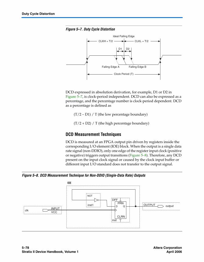
5–78 Altera CorporationStratix II Device Handbook, Volume 1 April 2006
Duty Cycle Distortion
Figure 5–7. Duty Cycle Distortion
DCD expressed in absolution derivation, for example, D1 or D2 in Figure 5–7, is clock-period independent. DCD can also be expressed as a percentage, and the percentage number is clock-period dependent. DCD as a percentage is defined as
(T/2 – D1) / T (the low percentage boundary)
(T/2 + D2) / T (the high percentage boundary)
DCD Measurement Techniques
DCD is measured at an FPGA output pin driven by registers inside the corresponding I/O element (IOE) block. When the output is a single data rate signal (non-DDIO), only one edge of the register input clock (positive or negative) triggers output transitions (Figure 5–8). Therefore, any DCD present on the input clock signal or caused by the clock input buffer or different input I/O standard does not transfer to the output signal.
Figure 5–8. DCD Measurement Technique for Non-DDIO (Single-Data Rate) Outputs
CLKH = T/2 CLKL = T/2
D1 D2
Falling Edge A
Ideal Falling Edge
Clock Period (T)
Falling Edge B
D Q
inst
PRN
CLRN
inst1
DFF
INPUTVCC
clk
NOT
OUTPUT output
IOE
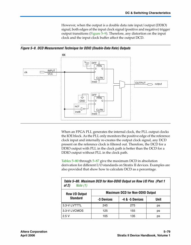
Altera Corporation 5–79April 2006 Stratix II Device Handbook, Volume 1
DC & Switching Characteristics
However, when the output is a double data rate input/output (DDIO) signal, both edges of the input clock signal (positive and negative) trigger output transitions (Figure 5–9). Therefore, any distortion on the input clock and the input clock buffer affect the output DCD.
Figure 5–9. DCD Measurement Technique for DDIO (Double-Data Rate) Outputs
When an FPGA PLL generates the internal clock, the PLL output clocks the IOE block. As the PLL only monitors the positive edge of the reference clock input and internally re-creates the output clock signal, any DCD present on the reference clock is filtered out. Therefore, the DCD for a DDIO output with PLL in the clock path is better than the DCD for a DDIO output without PLL in the clock path.
Tables 5–80 through 5–87 give the maximum DCD in absolution derivation for different I/O standards on Stratix II devices. Examples are also provided that show how to calculate DCD as a percentage.
D Q
inst2
PRN
CLRN
inst8
DFF
INPUTVCC
clk
NOT
OUTPUT output
IOE
D Q
inst3
PRN
CLRN
DFF
VCC
GND
Table 5–80. Maximum DCD for Non-DDIO Output on Row I/O Pins (Part 1 of 2) Note (1)
Row I/O Output Standard
Maximum DCD for Non-DDIO Output
-3 Devices -4 & -5 Devices Unit
3.3-V LVTTTL 245 275 ps
3.3-V LVCMOS 125 155 ps
2.5 V 105 135 ps
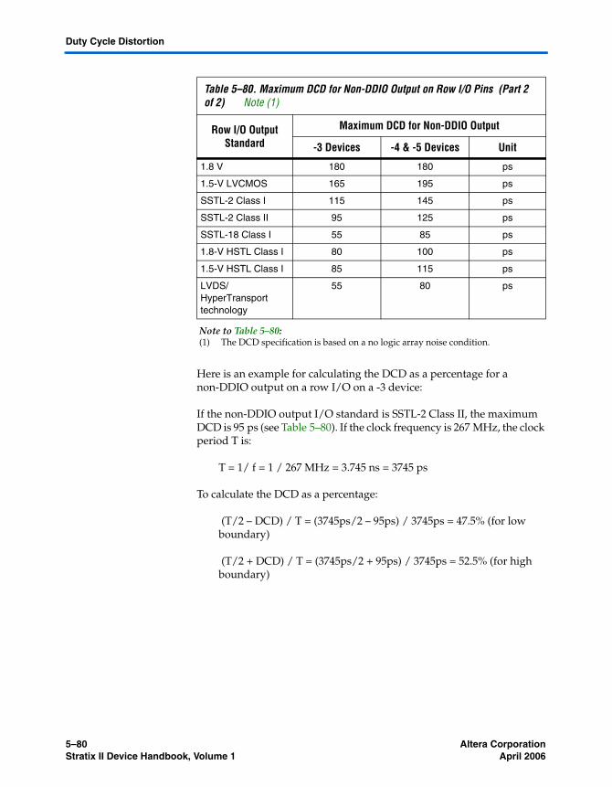
5–80 Altera CorporationStratix II Device Handbook, Volume 1 April 2006
Duty Cycle Distortion
Here is an example for calculating the DCD as a percentage for a non-DDIO output on a row I/O on a -3 device:
If the non-DDIO output I/O standard is SSTL-2 Class II, the maximum DCD is 95 ps (see Table 5–80). If the clock frequency is 267 MHz, the clock period T is:
T = 1/ f = 1 / 267 MHz = 3.745 ns = 3745 ps
To calculate the DCD as a percentage:
(T/2 – DCD) / T = (3745ps/2 – 95ps) / 3745ps = 47.5% (for low boundary)
(T/2 + DCD) / T = (3745ps/2 + 95ps) / 3745ps = 52.5% (for high boundary)
1.8 V 180 180 ps
1.5-V LVCMOS 165 195 ps
SSTL-2 Class I 115 145 ps
SSTL-2 Class II 95 125 ps
SSTL-18 Class I 55 85 ps
1.8-V HSTL Class I 80 100 ps
1.5-V HSTL Class I 85 115 ps
LVDS/ HyperTransport technology
55 80 ps
Note to Table 5–80:(1) The DCD specification is based on a no logic array noise condition.
Table 5–80. Maximum DCD for Non-DDIO Output on Row I/O Pins (Part 2 of 2) Note (1)
Row I/O Output Standard
Maximum DCD for Non-DDIO Output
-3 Devices -4 & -5 Devices Unit
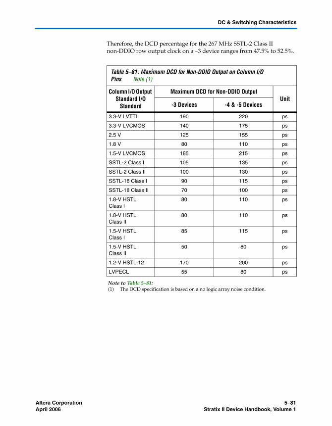
Altera Corporation 5–81April 2006 Stratix II Device Handbook, Volume 1
DC & Switching Characteristics
Therefore, the DCD percentage for the 267 MHz SSTL-2 Class II non-DDIO row output clock on a –3 device ranges from 47.5% to 52.5%.
Table 5–81. Maximum DCD for Non-DDIO Output on Column I/O Pins Note (1)
Column I/O Output Standard I/O
Standard
Maximum DCD for Non-DDIO OutputUnit
-3 Devices -4 & -5 Devices
3.3-V LVTTL 190 220 ps
3.3-V LVCMOS 140 175 ps
2.5 V 125 155 ps
1.8 V 80 110 ps
1.5-V LVCMOS 185 215 ps
SSTL-2 Class I 105 135 ps
SSTL-2 Class II 100 130 ps
SSTL-18 Class I 90 115 ps
SSTL-18 Class II 70 100 ps
1.8-V HSTL Class I
80 110 ps
1.8-V HSTL Class II
80 110 ps
1.5-V HSTL Class I
85 115 ps
1.5-V HSTL Class II
50 80 ps
1.2-V HSTL-12 170 200 ps
LVPECL 55 80 ps
Note to Table 5–81:(1) The DCD specification is based on a no logic array noise condition.
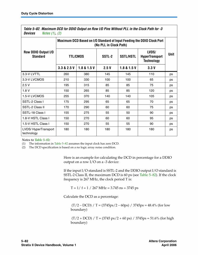
5–82 Altera CorporationStratix II Device Handbook, Volume 1 April 2006
Duty Cycle Distortion
Here is an example for calculating the DCD in percentage for a DDIO output on a row I/O on a -3 device:
If the input I/O standard is SSTL-2 and the DDIO output I/O standard is SSTL-2 Class II, the maximum DCD is 60 ps (see Table 5–82). If the clock frequency is 267 MHz, the clock period T is:
T = 1/ f = 1 / 267 MHz = 3.745 ns = 3745 ps
Calculate the DCD as a percentage:
(T/2 – DCD) / T = (3745ps/2 – 60ps) / 3745ps = 48.4% (for low boundary)
(T/2 + DCD) / T = (3745 ps/2 + 60 ps) / 3745ps = 51.6% (for high boundary)
Table 5–82. Maximum DCD for DDIO Output on Row I/O Pins Without PLL in the Clock Path for -3 Devices Notes (1), (2)
Row DDIO Output I/O Standard
Maximum DCD Based on I/O Standard of Input Feeding the DDIO Clock Port (No PLL in Clock Path)
UnitTTL/CMOS SSTL-2 SSTL/HSTLLVDS/
HyperTransport Technology
3.3 & 2.5 V 1.8 & 1.5 V 2.5 V 1.8 & 1.5 V 3.3 V
3.3-V LVTTL 260 380 145 145 110 ps
3.3-V LVCMOS 210 330 100 100 65 ps
2.5 V 195 315 85 85 75 ps
1.8 V 150 265 85 85 120 ps
1.5-V LVCMOS 255 370 140 140 105 ps
SSTL-2 Class I 175 295 65 65 70 ps
SSTL-2 Class II 170 290 60 60 75 ps
SSTL-18 Class I 155 275 55 50 90 ps
1.8-V HSTL Class I 150 270 60 60 95 ps
1.5-V HSTL Class I 150 270 55 55 90 ps
LVDS/ HyperTransport technology
180 180 180 180 180 ps
Notes to Table 5–82:(1) The information in Table 5–82 assumes the input clock has zero DCD.(2) The DCD specification is based on a no logic array noise condition.
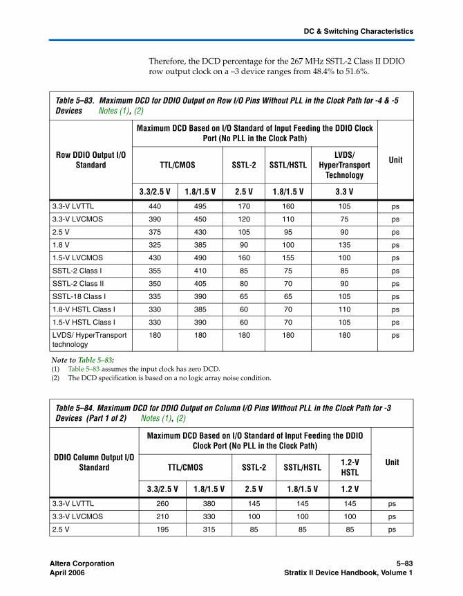
Altera Corporation 5–83April 2006 Stratix II Device Handbook, Volume 1
DC & Switching Characteristics
Therefore, the DCD percentage for the 267 MHz SSTL-2 Class II DDIO row output clock on a –3 device ranges from 48.4% to 51.6%.
Table 5–83. Maximum DCD for DDIO Output on Row I/O Pins Without PLL in the Clock Path for -4 & -5 Devices Notes (1), (2)
Row DDIO Output I/O Standard
Maximum DCD Based on I/O Standard of Input Feeding the DDIO Clock Port (No PLL in the Clock Path)
UnitTTL/CMOS SSTL-2 SSTL/HSTLLVDS/
HyperTransport Technology
3.3/2.5 V 1.8/1.5 V 2.5 V 1.8/1.5 V 3.3 V
3.3-V LVTTL 440 495 170 160 105 ps
3.3-V LVCMOS 390 450 120 110 75 ps
2.5 V 375 430 105 95 90 ps
1.8 V 325 385 90 100 135 ps
1.5-V LVCMOS 430 490 160 155 100 ps
SSTL-2 Class I 355 410 85 75 85 ps
SSTL-2 Class II 350 405 80 70 90 ps
SSTL-18 Class I 335 390 65 65 105 ps
1.8-V HSTL Class I 330 385 60 70 110 ps
1.5-V HSTL Class I 330 390 60 70 105 ps
LVDS/ HyperTransport technology
180 180 180 180 180 ps
Note to Table 5–83:(1) Table 5–83 assumes the input clock has zero DCD.(2) The DCD specification is based on a no logic array noise condition.
Table 5–84. Maximum DCD for DDIO Output on Column I/O Pins Without PLL in the Clock Path for -3 Devices (Part 1 of 2) Notes (1), (2)
DDIO Column Output I/O Standard
Maximum DCD Based on I/O Standard of Input Feeding the DDIO Clock Port (No PLL in the Clock Path)
UnitTTL/CMOS SSTL-2 SSTL/HSTL 1.2-V HSTL
3.3/2.5 V 1.8/1.5 V 2.5 V 1.8/1.5 V 1.2 V
3.3-V LVTTL 260 380 145 145 145 ps
3.3-V LVCMOS 210 330 100 100 100 ps
2.5 V 195 315 85 85 85 ps
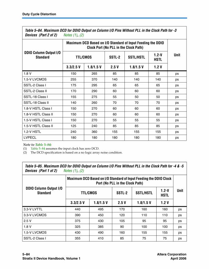
5–84 Altera CorporationStratix II Device Handbook, Volume 1 April 2006
Duty Cycle Distortion
1.8 V 150 265 85 85 85 ps
1.5-V LVCMOS 255 370 140 140 140 ps
SSTL-2 Class I 175 295 65 65 65 ps
SSTL-2 Class II 170 290 60 60 60 ps
SSTL-18 Class I 155 275 55 50 50 ps
SSTL-18 Class II 140 260 70 70 70 ps
1.8-V HSTL Class I 150 270 60 60 60 ps
1.8-V HSTL Class II 150 270 60 60 60 ps
1.5-V HSTL Class I 150 270 55 55 55 ps
1.5-V HSTL Class II 125 240 85 85 85 ps
1.2-V HSTL 240 360 155 155 155 ps
LVPECL 180 180 180 180 180 ps
Note to Table 5–84:(1) Table 5–84 assumes the input clock has zero DCD.(2) The DCD specification is based on a no logic array noise condition.
Table 5–85. Maximum DCD for DDIO Output on Column I/O Pins Without PLL in the Clock Path for -4 & -5 Devices (Part 1 of 2) Notes (1), (2)
DDIO Column Output I/O Standard
Maximum DCD Based on I/O Standard of Input Feeding the DDIO Clock Port (No PLL in the Clock Path)
UnitTTL/CMOS SSTL-2 SSTL/HSTL 1.2-V HSTL
3.3/2.5 V 1.8/1.5 V 2.5 V 1.8/1.5 V 1.2 V
3.3-V LVTTL 440 495 170 160 160 ps
3.3-V LVCMOS 390 450 120 110 110 ps
2.5 V 375 430 105 95 95 ps
1.8 V 325 385 90 100 100 ps
1.5-V LVCMOS 430 490 160 155 155 ps
SSTL-2 Class I 355 410 85 75 75 ps
Table 5–84. Maximum DCD for DDIO Output on Column I/O Pins Without PLL in the Clock Path for -3 Devices (Part 2 of 2) Notes (1), (2)
DDIO Column Output I/O Standard
Maximum DCD Based on I/O Standard of Input Feeding the DDIO Clock Port (No PLL in the Clock Path)
UnitTTL/CMOS SSTL-2 SSTL/HSTL 1.2-V HSTL
3.3/2.5 V 1.8/1.5 V 2.5 V 1.8/1.5 V 1.2 V
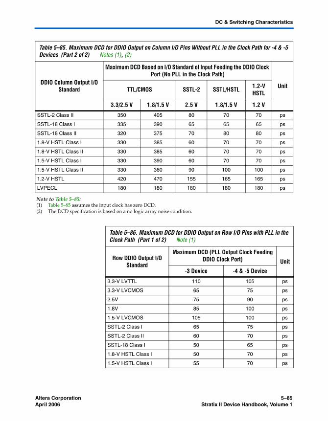
Altera Corporation 5–85April 2006 Stratix II Device Handbook, Volume 1
DC & Switching Characteristics
SSTL-2 Class II 350 405 80 70 70 ps
SSTL-18 Class I 335 390 65 65 65 ps
SSTL-18 Class II 320 375 70 80 80 ps
1.8-V HSTL Class I 330 385 60 70 70 ps
1.8-V HSTL Class II 330 385 60 70 70 ps
1.5-V HSTL Class I 330 390 60 70 70 ps
1.5-V HSTL Class II 330 360 90 100 100 ps
1.2-V HSTL 420 470 155 165 165 ps
LVPECL 180 180 180 180 180 ps
Note to Table 5–85:(1) Table 5–85 assumes the input clock has zero DCD.(2) The DCD specification is based on a no logic array noise condition.
Table 5–85. Maximum DCD for DDIO Output on Column I/O Pins Without PLL in the Clock Path for -4 & -5 Devices (Part 2 of 2) Notes (1), (2)
DDIO Column Output I/O Standard
Maximum DCD Based on I/O Standard of Input Feeding the DDIO Clock Port (No PLL in the Clock Path)
UnitTTL/CMOS SSTL-2 SSTL/HSTL 1.2-V HSTL
3.3/2.5 V 1.8/1.5 V 2.5 V 1.8/1.5 V 1.2 V
Table 5–86. Maximum DCD for DDIO Output on Row I/O Pins with PLL in the Clock Path (Part 1 of 2) Note (1)
Row DDIO Output I/O Standard
Maximum DCD (PLL Output Clock Feeding DDIO Clock Port) Unit
-3 Device -4 & -5 Device
3.3-V LVTTL 110 105 ps
3.3-V LVCMOS 65 75 ps
2.5V 75 90 ps
1.8V 85 100 ps
1.5-V LVCMOS 105 100 ps
SSTL-2 Class I 65 75 ps
SSTL-2 Class II 60 70 ps
SSTL-18 Class I 50 65 ps
1.8-V HSTL Class I 50 70 ps
1.5-V HSTL Class I 55 70 ps
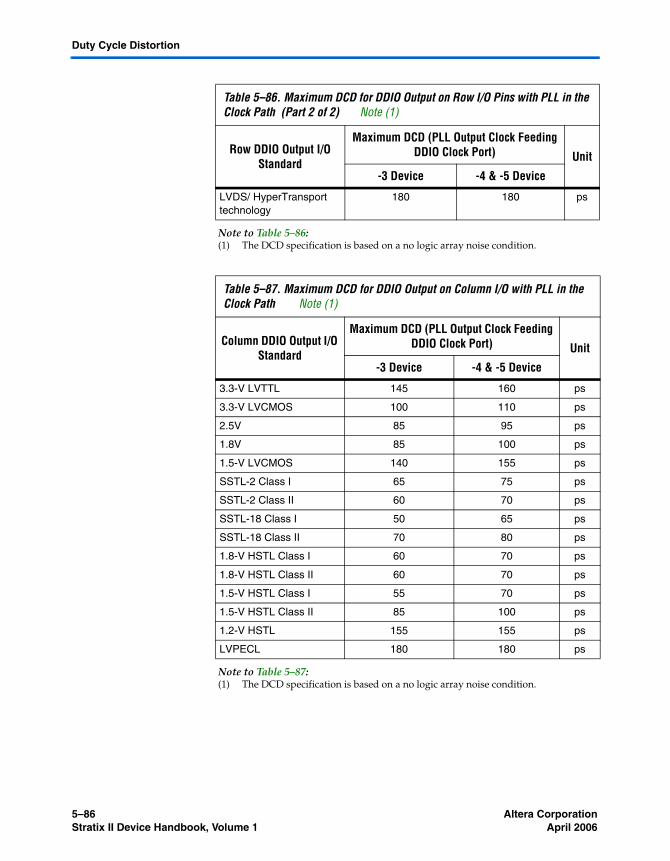
5–86 Altera CorporationStratix II Device Handbook, Volume 1 April 2006
Duty Cycle Distortion
LVDS/ HyperTransport technology
180 180 ps
Note to Table 5–86:(1) The DCD specification is based on a no logic array noise condition.
Table 5–87. Maximum DCD for DDIO Output on Column I/O with PLL in the Clock Path Note (1)
Column DDIO Output I/O Standard
Maximum DCD (PLL Output Clock Feeding DDIO Clock Port) Unit
-3 Device -4 & -5 Device
3.3-V LVTTL 145 160 ps
3.3-V LVCMOS 100 110 ps
2.5V 85 95 ps
1.8V 85 100 ps
1.5-V LVCMOS 140 155 ps
SSTL-2 Class I 65 75 ps
SSTL-2 Class II 60 70 ps
SSTL-18 Class I 50 65 ps
SSTL-18 Class II 70 80 ps
1.8-V HSTL Class I 60 70 ps
1.8-V HSTL Class II 60 70 ps
1.5-V HSTL Class I 55 70 ps
1.5-V HSTL Class II 85 100 ps
1.2-V HSTL 155 155 ps
LVPECL 180 180 ps
Note to Table 5–87:(1) The DCD specification is based on a no logic array noise condition.
Table 5–86. Maximum DCD for DDIO Output on Row I/O Pins with PLL in the Clock Path (Part 2 of 2) Note (1)
Row DDIO Output I/O Standard
Maximum DCD (PLL Output Clock Feeding DDIO Clock Port) Unit
-3 Device -4 & -5 Device
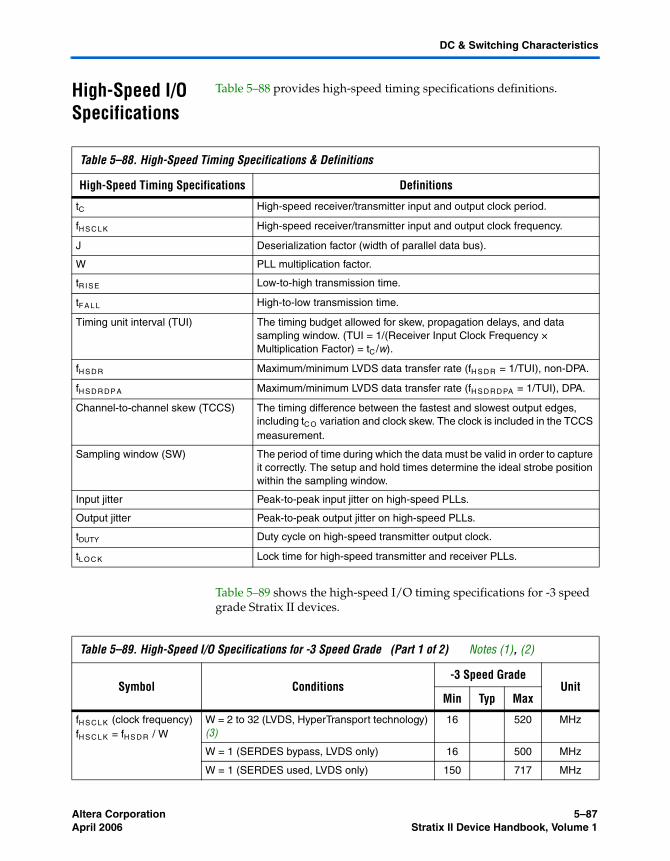
Altera Corporation 5–87April 2006 Stratix II Device Handbook, Volume 1
DC & Switching Characteristics
High-Speed I/O Specifications
Table 5–88 provides high-speed timing specifications definitions.
Table 5–89 shows the high-speed I/O timing specifications for -3 speed grade Stratix II devices.
Table 5–88. High-Speed Timing Specifications & Definitions
High-Speed Timing Specifications Definitions
tC High-speed receiver/transmitter input and output clock period.
fH S C L K High-speed receiver/transmitter input and output clock frequency.
J Deserialization factor (width of parallel data bus).
W PLL multiplication factor.
tR I S E Low-to-high transmission time.
tF A L L High-to-low transmission time.
Timing unit interval (TUI) The timing budget allowed for skew, propagation delays, and data sampling window. (TUI = 1/(Receiver Input Clock Frequency × Multiplication Factor) = tC /w).
fH S D R Maximum/minimum LVDS data transfer rate (fH S D R = 1/TUI), non-DPA.
fH S D R DP A Maximum/minimum LVDS data transfer rate (fH S D R D PA = 1/TUI), DPA.
Channel-to-channel skew (TCCS) The timing difference between the fastest and slowest output edges, including tC O variation and clock skew. The clock is included in the TCCS measurement.
Sampling window (SW) The period of time during which the data must be valid in order to capture it correctly. The setup and hold times determine the ideal strobe position within the sampling window.
Input jitter Peak-to-peak input jitter on high-speed PLLs.
Output jitter Peak-to-peak output jitter on high-speed PLLs.
tDUTY Duty cycle on high-speed transmitter output clock.
tL O C K Lock time for high-speed transmitter and receiver PLLs.
Table 5–89. High-Speed I/O Specifications for -3 Speed Grade (Part 1 of 2) Notes (1), (2)
Symbol Conditions-3 Speed Grade
UnitMin Typ Max
fH S C L K (clock frequency) fH S C L K = fHS D R / W
W = 2 to 32 (LVDS, HyperTransport technology) (3)
16 520 MHz
W = 1 (SERDES bypass, LVDS only) 16 500 MHz
W = 1 (SERDES used, LVDS only) 150 717 MHz
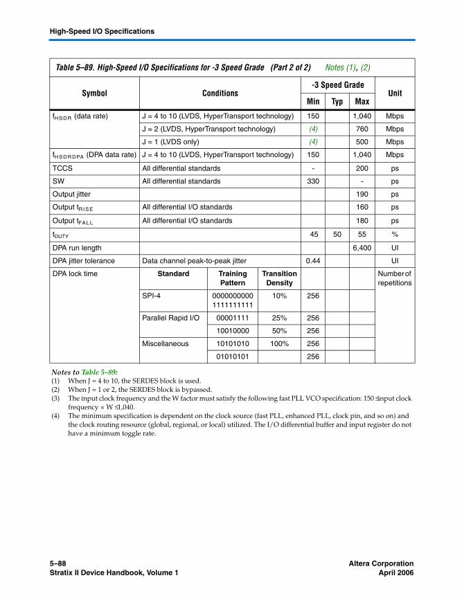
5–88 Altera CorporationStratix II Device Handbook, Volume 1 April 2006
High-Speed I/O Specifications
fH S D R (data rate) J = 4 to 10 (LVDS, HyperTransport technology) 150 1,040 Mbps
J = 2 (LVDS, HyperTransport technology) (4) 760 Mbps
J = 1 (LVDS only) (4) 500 Mbps
fH S D R DPA (DPA data rate) J = 4 to 10 (LVDS, HyperTransport technology) 150 1,040 Mbps
TCCS All differential standards - 200 ps
SW All differential standards 330 - ps
Output jitter 190 ps
Output tR I S E All differential I/O standards 160 ps
Output tFA L L All differential I/O standards 180 ps
tDUTY 45 50 55 %
DPA run length 6,400 UI
DPA jitter tolerance Data channel peak-to-peak jitter 0.44 UI
DPA lock time Standard Training Pattern
Transition Density
Number of repetitions
SPI-4 00000000001111111111
10% 256
Parallel Rapid I/O 00001111 25% 256
10010000 50% 256
Miscellaneous 10101010 100% 256
01010101 256
Notes to Table 5–89:(1) When J = 4 to 10, the SERDES block is used.(2) When J = 1 or 2, the SERDES block is bypassed.(3) The input clock frequency and the W factor must satisfy the following fast PLL VCO specification: 150 ≤ input clock
frequency × W ≤ 1,040.(4) The minimum specification is dependent on the clock source (fast PLL, enhanced PLL, clock pin, and so on) and
the clock routing resource (global, regional, or local) utilized. The I/O differential buffer and input register do not have a minimum toggle rate.
Table 5–89. High-Speed I/O Specifications for -3 Speed Grade (Part 2 of 2) Notes (1), (2)
Symbol Conditions-3 Speed Grade
UnitMin Typ Max
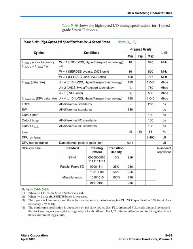
Altera Corporation 5–89April 2006 Stratix II Device Handbook, Volume 1
DC & Switching Characteristics
Table 5–90 shows the high-speed I/O timing specifications for -4 speed grade Stratix II devices.
Table 5–90. High-Speed I/O Specifications for -4 Speed Grade Notes (1), (2)
Symbol Conditions-4 Speed Grade
UnitMin Typ Max
fH S C L K (clock frequency) fH S C L K = fHS D R / W
W = 2 to 32 (LVDS, HyperTransport technology) (3)
16 520 MHz
W = 1 (SERDES bypass, LVDS only) 16 500 MHz
W = 1 (SERDES used, LVDS only) 150 717 MHz
fH S D R (data rate) J = 4 to 10 (LVDS, HyperTransport technology) 150 1,040 Mbps
J = 2 (LVDS, HyperTransport technology) (4) 760 Mbps
J = 1 (LVDS only) (4) 500 Mbps
fH S D R DPA (DPA data rate) J = 4 to 10 (LVDS, HyperTransport technology) 150 1,040 Mbps
TCCS All differential standards - 200 ps
SW All differential standards 330 - ps
Output jitter 190 ps
Output tR I S E All differential I/O standards 160 ps
Output tFA L L All differential I/O standards 180 ps
tDUTY 45 50 55 %
DPA run length 6,400 UI
DPA jitter tolerance Data channel peak-to-peak jitter 0.44 UI
DPA lock time Standard Training Pattern
Transition Density
Number of repetitions
SPI-4 00000000001111111111
10% 256
Parallel Rapid I/O 00001111 25% 256
10010000 50% 256
Miscellaneous 10101010 100% 256
01010101 256
Notes to Table 5–90:(1) When J = 4 to 10, the SERDES block is used.(2) When J = 1 or 2, the SERDES block is bypassed.(3) The input clock frequency and the W factor must satisfy the following fast PLL VCO specification: 150 ≤ input clock
frequency × W ≤ 1,040.(4) The minimum specification is dependent on the clock source (fast PLL, enhanced PLL, clock pin, and so on) and
the clock routing resource (global, regional, or local) utilized. The I/O differential buffer and input register do not have a minimum toggle rate.
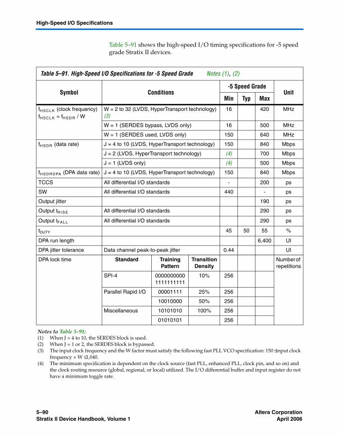
5–90 Altera CorporationStratix II Device Handbook, Volume 1 April 2006
High-Speed I/O Specifications
Table 5–91 shows the high-speed I/O timing specifications for -5 speed grade Stratix II devices.
Table 5–91. High-Speed I/O Specifications for -5 Speed Grade Notes (1), (2)
Symbol Conditions-5 Speed Grade
UnitMin Typ Max
fH S C L K (clock frequency) fH S C L K = fHS D R / W
W = 2 to 32 (LVDS, HyperTransport technology) (3)
16 420 MHz
W = 1 (SERDES bypass, LVDS only) 16 500 MHz
W = 1 (SERDES used, LVDS only) 150 640 MHz
fH S D R (data rate) J = 4 to 10 (LVDS, HyperTransport technology) 150 840 Mbps
J = 2 (LVDS, HyperTransport technology) (4) 700 Mbps
J = 1 (LVDS only) (4) 500 Mbps
fH S D R DPA (DPA data rate) J = 4 to 10 (LVDS, HyperTransport technology) 150 840 Mbps
TCCS All differential I/O standards - 200 ps
SW All differential I/O standards 440 - ps
Output jitter 190 ps
Output tR I S E All differential I/O standards 290 ps
Output tFA L L All differential I/O standards 290 ps
tDUTY 45 50 55 %
DPA run length 6,400 UI
DPA jitter tolerance Data channel peak-to-peak jitter 0.44 UI
DPA lock time Standard Training Pattern
Transition Density
Number of repetitions
SPI-4 00000000001111111111
10% 256
Parallel Rapid I/O 00001111 25% 256
10010000 50% 256
Miscellaneous 10101010 100% 256
01010101 256
Notes to Table 5–91:(1) When J = 4 to 10, the SERDES block is used.(2) When J = 1 or 2, the SERDES block is bypassed.(3) The input clock frequency and the W factor must satisfy the following fast PLL VCO specification: 150 ≤ input clock
frequency × W ≤ 1,040.(4) The minimum specification is dependent on the clock source (fast PLL, enhanced PLL, clock pin, and so on) and
the clock routing resource (global, regional, or local) utilized. The I/O differential buffer and input register do not have a minimum toggle rate.
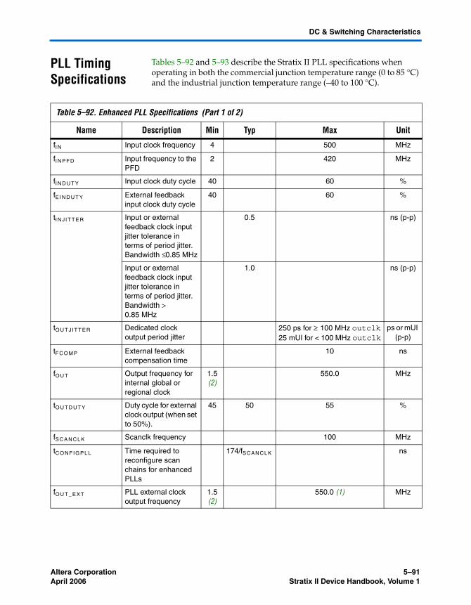
Altera Corporation 5–91April 2006 Stratix II Device Handbook, Volume 1
DC & Switching Characteristics
PLL Timing Specifications
Tables 5–92 and 5–93 describe the Stratix II PLL specifications when operating in both the commercial junction temperature range (0 to 85 °C) and the industrial junction temperature range (–40 to 100 °C).
Table 5–92. Enhanced PLL Specifications (Part 1 of 2)
Name Description Min Typ Max Unit
fI N Input clock frequency 4 500 MHz
fI N P F D Input frequency to the PFD
2 420 MHz
fI N D UT Y Input clock duty cycle 40 60 %
fE I ND U T Y External feedback input clock duty cycle
40 60 %
tI N J I T T E R Input or external feedback clock input jitter tolerance in terms of period jitter.Bandwidth ≤ 0.85 MHz
0.5 ns (p-p)
Input or external feedback clock input jitter tolerance in terms of period jitter.Bandwidth > 0.85 MHz
1.0 ns (p-p)
tO U T J I T T E R Dedicated clock output period jitter
250 ps for ≥ 100 MHz outclk25 mUI for < 100 MHz outclk
ps or mUI (p-p)
tF C O M P External feedback compensation time
10 ns
fO U T Output frequency for internal global or regional clock
1.5 (2)
550.0 MHz
tO U T D UT Y Duty cycle for external clock output (when set to 50%).
45 50 55 %
fS C A N C L K Scanclk frequency 100 MHz
tC O NF I G P L L Time required to reconfigure scan chains for enhanced PLLs
174/fSCANCLK ns
fO U T _ E X T PLL external clock output frequency
1.5 (2)
550.0 (1) MHz
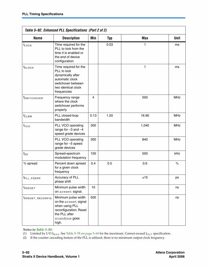
5–92 Altera CorporationStratix II Device Handbook, Volume 1 April 2006
PLL Timing Specifications
tL O C K Time required for the PLL to lock from the time it is enabled or the end of device configuration
0.03 1 ms
tD L O C K Time required for the PLL to lock dynamically after automatic clock switchover between two identical clock frequencies
1 ms
fS W I T CH OV E R Frequency range where the clock switchover performs properly
4 500 MHz
fC L B W PLL closed-loop bandwidth
0.13 1.20 16.90 MHz
fV C O PLL VCO operating range for –3 and –4 speed grade devices
300 1,040 MHz
PLL VCO operating range for –5 speed grade devices
300 840 MHz
fS S Spread-spectrum modulation frequency
100 500 kHz
% spread Percent down spread for a given clock frequency
0.4 0.5 0.6 %
tP L L _ P S E R R Accuracy of PLL phase shift
±15 ps
tA R E S E T Minimum pulse width on areset signal.
10 ns
tA R E S E T _ RE C O NF I G Minimum pulse width on the areset signal when using PLL reconfiguration. Reset the PLL after scandone goes high.
500 ns
Notes to Table 5–92:(1) Limited by I/O fM A X. See Table 5–78 on page 5–69 for the maximum. Cannot exceed fO U T specification.(2) If the counter cascading feature of the PLL is utilized, there is no minimum output clock frequency.
Table 5–92. Enhanced PLL Specifications (Part 2 of 2)
Name Description Min Typ Max Unit
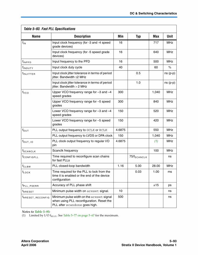
Altera Corporation 5–93April 2006 Stratix II Device Handbook, Volume 1
DC & Switching Characteristics
Table 5–93. Fast PLL Specifications
Name Description Min Typ Max Unit
fI N Input clock frequency (for -3 and -4 speed grade devices)
16 717 MHz
Input clock frequency (for -5 speed grade devices)
16 640 MHz
fI N P F D Input frequency to the PFD 16 500 MHz
fI N D UT Y Input clock duty cycle 40 60 %
tI N J I T T E R Input clock jitter tolerance in terms of period jitter. Bandwidth ≤ 2 MHz
0.5 ns (p-p)
Input clock jitter tolerance in terms of period jitter. Bandwidth > 2 MHz
1.0 ns (p-p)
fV C O Upper VCO frequency range for –3 and –4 speed grades
300 1,040 MHz
Upper VCO frequency range for –5 speed grades
300 840 MHz
Lower VCO frequency range for –3 and –4 speed grades
150 520 MHz
Lower VCO frequency range for –5 speed grades
150 420 MHz
fO U T PLL output frequency to GCLK or RCLK 4.6875 550 MHz
PLL output frequency to LVDS or DPA clock 150 1,040 MHz
fO U T _ I O PLL clock output frequency to regular I/O pin
4.6875 (1) MHz
fS C A N C L K Scanclk frequency 100 MHz
tC O NF I G P L L Time required to reconfigure scan chains for fast PLLs
75/fS CA N CL K ns
fC L B W PLL closed-loop bandwidth 1.16 5.00 28.00 MHz
tL O C K Time required for the PLL to lock from the time it is enabled or the end of the device configuration
0.03 1.00 ms
tP L L _ P S E R R Accuracy of PLL phase shift ±15 ps
tA R E S E T Minimum pulse width on areset signal. 10 ns
tA R E S E T _ RE C O NF I G Minimum pulse width on the areset signal when using PLL reconfiguration. Reset the PLL after scandone goes high.
500 ns
Notes to Table 5–93:(1) Limited by I/O fM A X. See Table 5–77 on page 5–67 for the maximum.
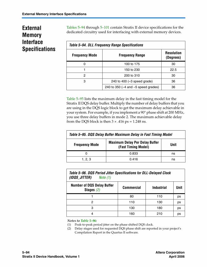
5–94 Altera CorporationStratix II Device Handbook, Volume 1 April 2006
External Memory Interface Specifications
External Memory Interface Specifications
Tables 5–94 through 5–101 contain Stratix II device specifications for the dedicated circuitry used for interfacing with external memory devices.
Table 5–95 lists the maximum delay in the fast timing model for the Stratix II DQS delay buffer. Multiply the number of delay buffers that you are using in the DQS logic block to get the maximum delay achievable in your system. For example, if you implement a 90° phase shift at 200 MHz, you use three delay buffers in mode 2. The maximum achievable delay from the DQS block is then 3 × .416 ps = 1.248 ns.
Table 5–94. DLL Frequency Range Specifications
Frequency Mode Frequency Range Resolution (Degrees)
0 100 to 175 30
1 150 to 230 22.5
2 200 to 310 30
3 240 to 400 (–3 speed grade) 36
240 to 350 (–4 and –5 speed grades) 36
Table 5–95. DQS Delay Buffer Maximum Delay in Fast Timing Model
Frequency Mode Maximum Delay Per Delay Buffer (Fast Timing Model) Unit
0 0.833 ns
1, 2, 3 0.416 ns
Table 5–96. DQS Period Jitter Specifications for DLL-Delayed Clock (tDQS_JITTER) Note (1)
Number of DQS Delay Buffer Stages (2) Commercial Industrial Unit
1 80 110 ps
2 110 130 ps
3 130 180 ps
4 160 210 ps
Notes to Table 5–96:(1) Peak-to-peak period jitter on the phase shifted DQS clock.(2) Delay stages used for requested DQS phase shift are reported in your project’s
Compilation Report in the Quartus II software.
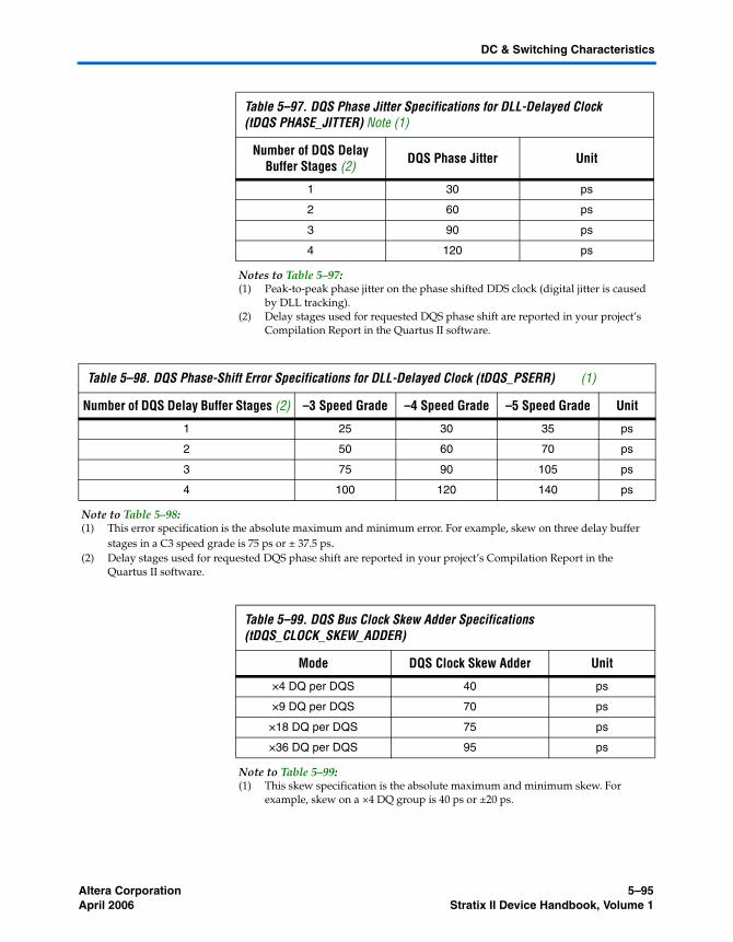
Altera Corporation 5–95April 2006 Stratix II Device Handbook, Volume 1
DC & Switching Characteristics
Table 5–97. DQS Phase Jitter Specifications for DLL-Delayed Clock(tDQS PHASE_JITTER) Note (1)
Number of DQS Delay Buffer Stages (2) DQS Phase Jitter Unit
1 30 ps
2 60 ps
3 90 ps
4 120 ps
Notes to Table 5–97:(1) Peak-to-peak phase jitter on the phase shifted DDS clock (digital jitter is caused
by DLL tracking).(2) Delay stages used for requested DQS phase shift are reported in your project’s
Compilation Report in the Quartus II software.
Table 5–98. DQS Phase-Shift Error Specifications for DLL-Delayed Clock (tDQS_PSERR) (1)
Number of DQS Delay Buffer Stages (2) –3 Speed Grade –4 Speed Grade –5 Speed Grade Unit
1 25 30 35 ps
2 50 60 70 ps
3 75 90 105 ps
4 100 120 140 ps
Note to Table 5–98:(1) This error specification is the absolute maximum and minimum error. For example, skew on three delay buffer
stages in a C3 speed grade is 75 ps or ± 37.5 ps.(2) Delay stages used for requested DQS phase shift are reported in your project’s Compilation Report in the
Quartus II software.
Table 5–99. DQS Bus Clock Skew Adder Specifications (tDQS_CLOCK_SKEW_ADDER)
Mode DQS Clock Skew Adder Unit
×4 DQ per DQS 40 ps
×9 DQ per DQS 70 ps
×18 DQ per DQS 75 ps
×36 DQ per DQS 95 ps
Note to Table 5–99:(1) This skew specification is the absolute maximum and minimum skew. For
example, skew on a ×4 DQ group is 40 ps or ±20 ps.
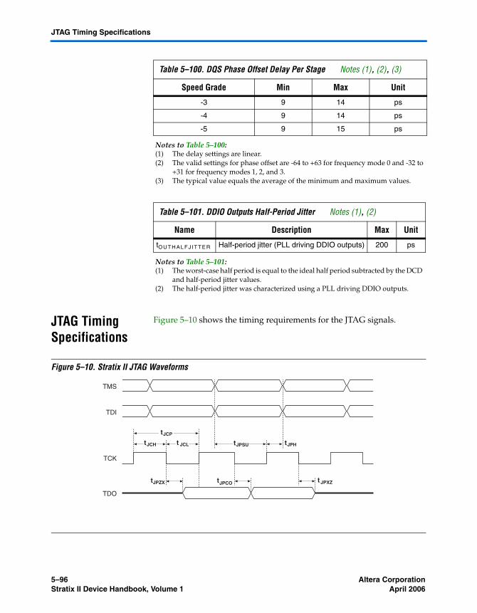
5–96 Altera CorporationStratix II Device Handbook, Volume 1 April 2006
JTAG Timing Specifications
JTAG Timing Specifications
Figure 5–10 shows the timing requirements for the JTAG signals.
Figure 5–10. Stratix II JTAG Waveforms
Table 5–100. DQS Phase Offset Delay Per Stage Notes (1), (2), (3)
Speed Grade Min Max Unit
-3 9 14 ps
-4 9 14 ps
-5 9 15 ps
Notes to Table 5–100:(1) The delay settings are linear.(2) The valid settings for phase offset are -64 to +63 for frequency mode 0 and -32 to
+31 for frequency modes 1, 2, and 3.(3) The typical value equals the average of the minimum and maximum values.
Table 5–101. DDIO Outputs Half-Period Jitter Notes (1), (2)
Name Description Max Unit
tO U T H A L F J I T T E R Half-period jitter (PLL driving DDIO outputs) 200 ps
Notes to Table 5–101:(1) The worst-case half period is equal to the ideal half period subtracted by the DCD
and half-period jitter values.(2) The half-period jitter was characterized using a PLL driving DDIO outputs.
TDO
TCK
tJPZX tJPCO
tJPH
t JPXZ
tJCP
tJPSU t JCL tJCH
TDI
TMS
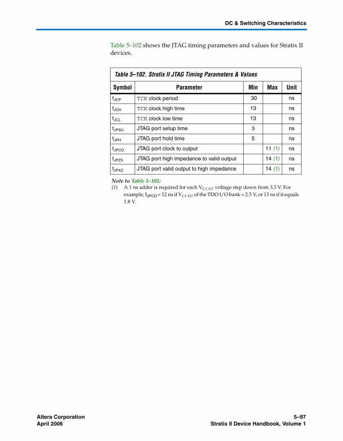
Altera Corporation 5–97April 2006 Stratix II Device Handbook, Volume 1
DC & Switching Characteristics
Table 5–102 shows the JTAG timing parameters and values for Stratix II devices.
Table 5–102. Stratix II JTAG Timing Parameters & Values
Symbol Parameter Min Max Unit
tJCP TCK clock period 30 ns
tJCH TCK clock high time 13 ns
tJCL TCK clock low time 13 ns
tJPSU JTAG port setup time 3 ns
tJPH JTAG port hold time 5 ns
tJPCO JTAG port clock to output 11 (1) ns
tJPZX JTAG port high impedance to valid output 14 (1) ns
tJPXZ JTAG port valid output to high impedance 14 (1) ns
Note to Table 5–102:(1) A 1 ns adder is required for each VC C I O voltage step down from 3.3 V. For
example, tJPCO = 12 ns if VC C I O of the TDO I/O bank = 2.5 V, or 13 ns if it equals 1.8 V.
5–98 Altera CorporationStratix II Device Handbook, Volume 1 April 2006
JTAG Timing Specifications
Altera Corporation 6–1January 2005
6. Reference & OrderingInformation
Software Stratix® II devices are supported by the Altera® Quartus® II design software, which provides a comprehensive environment for system-on-a-programmable-chip (SOPC) design. The Quartus II software includes HDL and schematic design entry, compilation and logic synthesis, full simulation and advanced timing analysis, SignalTap® II logic analyzer, and device configuration. See the Quartus II Handbook for more information on the Quartus II software features.
The Quartus II software supports the Windows XP/2000/NT/98, Sun Solaris, Linux Red Hat v7.1 and HP-UX operating systems. It also supports seamless integration with industry-leading EDA tools through the NativeLink® interface.
Device Pin-Outs Device pin-outs for Stratix II devices are available on the Altera web site at (www.altera.com).
Ordering Information
Figure 6–1 describes the ordering codes for Stratix II devices. For more information on a specific package, refer to the Package Information for Stratix II & Stratix II GX Devices chapter of the Stratix II Device Handbook, Volume 2 or the Stratix II GX Device Handbook, Volume 2.
SII51006-2.0
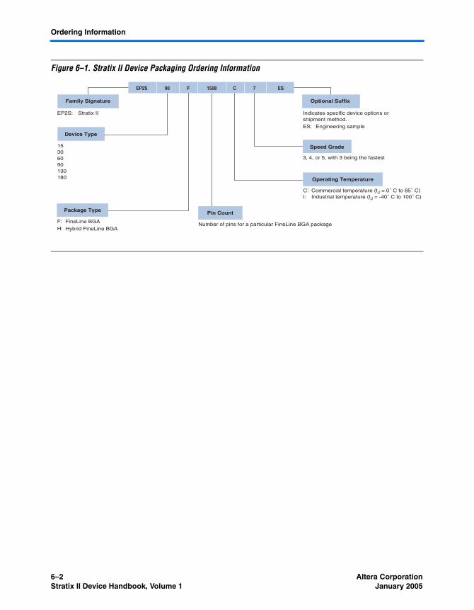
6–2 Altera CorporationStratix II Device Handbook, Volume 1 January 2005
Ordering Information
Figure 6–1. Stratix II Device Packaging Ordering Information
Device Type
Package Type
3, 4, or 5, with 3 being the fastest
Number of pins for a particular FineLine BGA package
ES:
F: FineLine BGAH: Hybrid FineLine BGA
EP2S: Stratix II
15306090130180
C:I:
Commercial temperature (tJ = 0˚ C to 85˚ C)Industrial temperature (tJ = -40˚ C to 100˚ C)
Optional SuffixFamily Signature
Operating Temperature
Speed Grade
Pin Count
Engineering sample
7EP2S 90 C1508F ES
Indicates specific device options or shipment method.