Embed Size (px)
Citation preview
Stratix IV Device Handbook Volume 1February 2011
SIV51001-3.2
© 2011 Altera Corporation. All rights reserved. ALTERA, ARRand/or trademarks of Altera Corporation in the U.S. and otherwww.altera.com/common/legal.html. Altera warrants performreserves the right to make changes to any products and servicesinformation, product, or service described herein except as expspecifications before relying on any published information and
February 2011SIV51001-3.2
1. Overview for the Stratix IV DeviceFamily
Altera® Stratix® IV FPGAs deliver a breakthrough level of system bandwidth and power efficiency for high-end applications, allowing you to innovate without compromise. Stratix IV FPGAs are based on the Taiwan Semiconductor Manufacturing Company (TSMC) 40-nm process technology and surpass all other high-end FPGAs, with the highest logic density, most transceivers, and lowest power requirements.
The Stratix IV device family contains three optimized variants to meet different application requirements:
■ Stratix IV E (Enhanced) FPGAs—up to 813,050 logic elements (LEs), 33,294 Kbits RAM, and 1,288 18 × 18 bit multipliers
■ Stratix IV GX transceiver FPGAs—up to 531,200 LEs, 27,376 Kbits RAM, 1,288 18 × 18-bit multipliers, and 48 full-duplex clock data recovery (CDR)-based transceivers at up to 8.5 Gbps
■ Stratix IV GT—up to 531,200 LEs, 27,376 Kbits RAM, 1,288 18 × 18-bit multipliers, and 48 full-duplex CDR-based transceivers at up to 11.3 Gbps
The complete Altera high-end solution includes the lowest risk, lowest total cost path to volume using HardCopy® IV ASICs for all the family variants, a comprehensive portfolio of application solutions customized for end-markets, and the industry leading Quartus® II software to increase productivity and performance.
f For information about upcoming Stratix IV device features, refer to the Upcoming Stratix IV Device Features document.
f For information about changes to the currently published Stratix IV Device Handbook, refer to the Addendum to the Stratix IV Device Handbook chapter.
This chapter contains the following sections:
■ “Feature Summary” on page 1–2
■ “Architecture Features” on page 1–6
■ “Integrated Software Platform” on page 1–19
■ “Ordering Information” on page 1–19
Subscribe
IA, CYCLONE, HARDCOPY, MAX, MEGACORE, NIOS, QUARTUS and STRATIX are Reg. U.S. Pat. & Tm. Off. countries. All other trademarks and service marks are the property of their respective holders as described at
ance of its semiconductor products to current specifications in accordance with Altera’s standard warranty, but at any time without notice. Altera assumes no responsibility or liability arising out of the application or use of any ressly agreed to in writing by Altera. Altera customers are advised to obtain the latest version of device before placing orders for products or services.
1–2 Chapter 1: Overview for the Stratix IV Device FamilyFeature Summary
Feature SummaryThe following list summarizes the Stratix IV device family features:
■ Up to 48 full-duplex CDR-based transceivers in Stratix IV GX and GT devices supporting data rates up to 8.5 Gbps and 11.3 Gbps, respectively
■ Dedicated circuitry to support physical layer functionality for popular serial protocols, such as PCI Express (PCIe) (PIPE) Gen1 and Gen2, Gbps Ethernet (GbE), Serial RapidIO, SONET/SDH, XAUI/HiGig, (OIF) CEI-6G, SD/HD/3G-SDI, Fibre Channel, SFI-5, and Interlaken
■ Complete PCIe protocol solution with embedded PCIe hard IP blocks that implement PHY-MAC layer, Data Link layer, and Transaction layer functionality
f For more information, refer to the PCI Express Compiler User Guide.
■ Programmable transmitter pre-emphasis and receiver equalization circuitry to compensate for frequency-dependent losses in the physical medium
■ Typical physical medium attachment (PMA) power consumption of 100 mW at 3.125 Gbps and 135 mW at 6.375 Gbps per channel
■ 72,600 to 813,050 equivalent LEs per device
■ 7,370 to 33,294 Kbits of enhanced TriMatrix memory consisting of three RAM block sizes to implement true dual-port memory and FIFO buffers
■ High-speed digital signal processing (DSP) blocks configurable as 9 × 9-bit, 12 × 12-bit, 18 × 18-bit, and 36 × 36-bit full-precision multipliers at up to 600 MHz
■ Up to 16 global clocks (GCLK), 88 regional clocks (RCLK), and 132 periphery clocks (PCLK) per device
■ Programmable power technology that minimizes power while maximizing device performance
■ Up to 1,120 user I/O pins arranged in 24 modular I/O banks that support a wide range of single-ended and differential I/O standards
■ Support for high-speed external memory interfaces including DDR, DDR2, DDR3 SDRAM, RLDRAM II, QDR II, and QDR II+ SRAM on up to 24 modular I/O banks
■ High-speed LVDS I/O support with serializer/deserializer (SERDES), dynamic phase alignment (DPA), and soft-CDR circuitry at data rates up to 1.6 Gbps
■ Support for source-synchronous bus standards, including SGMII, GbE, SPI-4 Phase 2 (POS-PHY Level 4), SFI-4.1, XSBI, UTOPIA IV, NPSI, and CSIX-L1
■ Pinouts for Stratix IV E devices designed to allow migration of designs from Stratix III to Stratix IV E with minimal PCB impact
Stratix IV Device Handbook Volume 1 February 2011 Altera Corporation
Chapter 1: Overview for the Stratix IV Device Family 1–3Feature Summary
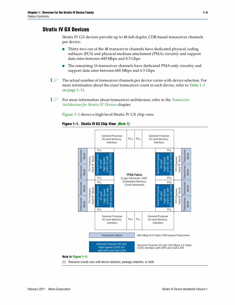
Stratix IV GX DevicesStratix IV GX devices provide up to 48 full-duplex CDR-based transceiver channels per device:
■ Thirty-two out of the 48 transceiver channels have dedicated physical coding sublayer (PCS) and physical medium attachment (PMA) circuitry and support data rates between 600 Mbps and 8.5 Gbps
■ The remaining 16 transceiver channels have dedicated PMA-only circuitry and support data rates between 600 Mbps and 6.5 Gbps
1 The actual number of transceiver channels per device varies with device selection. For more information about the exact transceiver count in each device, refer to Table 1–1 on page 1–11.
1 For more information about transceiver architecture, refer to the Transceiver Architecture for Stratix IV Devices chapter.
Figure 1–1 shows a high-level Stratix IV GX chip view.
Figure 1–1. Stratix IV GX Chip View (Note 1)
Note to Figure 1–1:
(1) Resource counts vary with device selection, package selection, or both.
General PurposeI/O and Memory
Interface
600 Mbps-8.5 Gbps CDR-based Transceiver
General Purpose I/O and 150 Mbps-1.6 Gbps LVDS interface with DPA and Soft-CDR
Tran
scei
ver
Blo
ckTr
ansc
eive
rB
lock
Tran
scei
ver
Blo
ckTr
ansc
eive
rB
lock
PC
I Exp
ress
Har
d IP
Blo
ckP
CI E
xpre
ssH
ard
IP B
lock
PC
I Exp
ress
Har
d IP
Blo
ckP
CI E
xpre
ssH
ard
IP B
lock
General PurposeI/O and Memory
Interface
PLL
PLL
PLL
PLL
PLL PLL
General PurposeI/O and Memory
Interface
General PurposeI/O and Memory
InterfacePLL PLL
FPGA Fabric(Logic Elements, DSP,
Embedded Memory,Clock Networks)
Transceiver Block
General Purpose I/O and High-Speed LVDS I/O with DPA and Soft CDR
Gen
eral
Pur
pose
I/O
and
H
igh-
Spe
ed
LVD
S I/
O w
ith
DPA
and
Sof
t CD
R
PLL
PLL
PLL
PLL
Tran
scei
ver
Blo
ckTr
ansc
eive
rB
lock
Tran
scei
ver
Blo
ckTr
ansc
eive
rB
lock
Gen
eral
Pur
pose
I/O
and
H
igh-
Spe
ed
LVD
S I/
O w
ith
DPA
and
Sof
t CD
R
Gen
eral
Pur
pose
I/O
and
H
igh-
Spe
ed
LVD
S I/
O w
ith
DPA
and
Sof
t CD
R
Gen
eral
Pur
pose
I/O
and
H
igh-
Spe
ed
LVD
S I/
O w
ith
DPA
and
Sof
t CD
R
February 2011 Altera Corporation Stratix IV Device Handbook Volume 1
1–4 Chapter 1: Overview for the Stratix IV Device FamilyFeature Summary
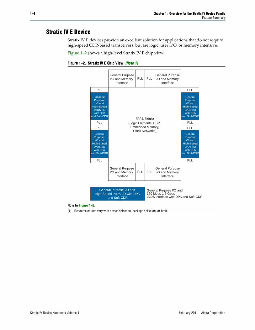
Stratix IV E DeviceStratix IV E devices provide an excellent solution for applications that do not require high-speed CDR-based transceivers, but are logic, user I/O, or memory intensive.
Figure 1–2 shows a high-level Stratix IV E chip view.
Figure 1–2. Stratix IV E Chip View (Note 1)
Note to Figure 1–2:(1) Resource counts vary with device selection, package selection, or both.
General PurposeI/O and Memory
Interface
General Purpose I/O and 150 Mbps-1.6 Gbps LVDS interface with DPA and Soft-CDR
General Purpose I/O and
High-Speed LVDS I/O with DPA
and Soft-CDR
General PurposeI/O and Memory
Interface
PLL
PLL
PLL
PLL
PLL
PLL
PLL
PLL
PLL PLL
General PurposeI/O and Memory
Interface
General PurposeI/O and Memory
InterfacePLL PLL
FPGA Fabric(Logic Elements, DSP,
Embedded Memory,Clock Networks)
General Purpose I/O and High-Speed LVDS I/O with DPA
and Soft-CDR
General Purpose I/O and
High-Speed LVDS I/O with DPA
and Soft-CDR
General Purpose I/O and
High-Speed LVDS I/O with DPA
and Soft-CDR
General Purpose I/O and
High-Speed LVDS I/O with DPA
and Soft-CDR
Stratix IV Device Handbook Volume 1 February 2011 Altera Corporation
Chapter 1: Overview for the Stratix IV Device Family 1–5Feature Summary
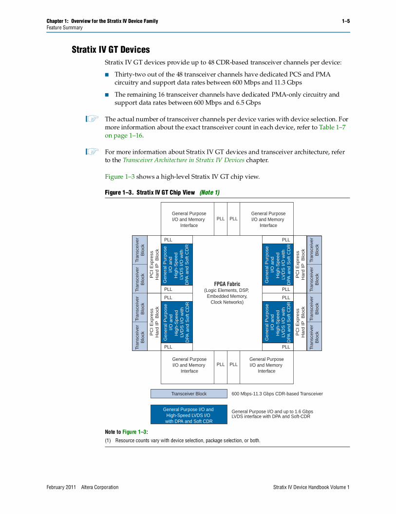
Stratix IV GT DevicesStratix IV GT devices provide up to 48 CDR-based transceiver channels per device:
■ Thirty-two out of the 48 transceiver channels have dedicated PCS and PMA circuitry and support data rates between 600 Mbps and 11.3 Gbps
■ The remaining 16 transceiver channels have dedicated PMA-only circuitry and support data rates between 600 Mbps and 6.5 Gbps
1 The actual number of transceiver channels per device varies with device selection. For more information about the exact transceiver count in each device, refer to Table 1–7 on page 1–16.
1 For more information about Stratix IV GT devices and transceiver architecture, refer to the Transceiver Architecture in Stratix IV Devices chapter.
Figure 1–3 shows a high-level Stratix IV GT chip view.
Figure 1–3. Stratix IV GT Chip View (Note 1)
Note to Figure 1–3:(1) Resource counts vary with device selection, package selection, or both.
General PurposeI/O and Memory
Interface
600 Mbps-11.3 Gbps CDR-based Transceiver
General Purpose I/O and up to 1.6 Gbps LVDS interface with DPA and Soft-CDR
PC
I E
xpre
ssH
ard
IP
B
lock
PC
I E
xpre
ssH
ard
IP
B
lock
PC
I E
xpre
ssH
ard
IP
B
lock
PC
I E
xpre
ssH
ard
IP
B
lock
Tra
nsc
eiv
er
Blo
ckTr
an
sce
ive
rB
lock
Tra
nsc
eiv
er
Blo
ckTr
an
sce
ive
rB
lock
General PurposeI/O and Memory
Interface
PLL
PLL
PLL
PLL
PLL PLL
General PurposeI/O and Memory
Interface
General PurposeI/O and Memory
InterfacePLL PLL
FPGA Fabric(Logic Elements, DSP,
Embedded Memory,Clock Networks)
Transceiver Block
General Purpose I/O and High-Speed LVDS I/O with DPA and Soft CDR
Ge
ne
ral P
urp
ose
I/O
an
dH
igh
-Sp
ee
dLV
DS
I/O
with
DPA
an
d S
oft
CD
R
PLL
PLL
PLL
PLL
Ge
ne
ral P
urp
ose
I/O
an
dH
igh
-Sp
ee
dLV
DS
I/O
with
DPA
an
d S
oft
CD
R
Ge
ne
ral P
urp
ose
I/O
an
dH
igh
-Sp
ee
dLV
DS
I/O
with
DPA
an
d S
oft
CD
R
Ge
ne
ral P
urp
ose
I/O
an
dH
igh
-Sp
ee
dLV
DS
I/O
with
DPA
an
d S
oft
CD
R
Tra
nsc
eiv
er
Blo
ckTr
an
sce
ive
rB
lock
Tra
nsc
eiv
er
Blo
ckTr
an
sce
ive
rB
lock
February 2011 Altera Corporation Stratix IV Device Handbook Volume 1
1–6 Chapter 1: Overview for the Stratix IV Device FamilyArchitecture Features
Architecture FeaturesThe Stratix IV device family features are divided into high-speed transceiver features and FPGA fabric and I/O features.
1 The high-speed transceiver features apply only to Stratix IV GX and Stratix IV GT devices.
High-Speed Transceiver FeaturesThe following sections describe high-speed transceiver features for Stratix IV GX and GT devices.
Highest Aggregate Data BandwidthUp to 48 full-duplex transceiver channels supporting data rates up to 8.5 Gbps in Stratix IV GX devices and up to 11.3 Gbps in Stratix IV GT devices.
Wide Range of Protocol SupportPhysical layer support for the following serial protocols:
■ Stratix IV GX—PCIe Gen1 and Gen2, GbE, Serial RapidIO, SONET/SDH, XAUI/HiGig, (OIF) CEI-6G, SD/HD/3G-SDI, Fibre Channel, SFI-5, GPON, SAS/SATA, HyperTransport 1.0 and 3.0, and Interlaken
■ Stratix IV GT—40G/100G Ethernet, SFI-S, Interlaken, SFI-5.1, Serial RapidIO, SONET/SDH, XAUI/HiGig, (OIF) CEI-6G, 3G-SDI, and Fibre Channel
■ Extremely flexible and easy-to-configure transceiver data path to implement proprietary protocols
■ PCIe Support
■ Complete PCIe Gen1 and Gen2 protocol stack solution compliant to PCI Express base specification 2.0 that includes PHY-MAC, Data Link, and transaction layer circuitry embedded in PCI Express hard IP blocks
f For more information, refer to the PCI Express Compiler User Guide.
■ Root complex and end-point applications
■ ×1, ×4, and ×8 lane configurations
■ PIPE 2.0-compliant interface
■ Embedded circuitry to switch between Gen1 and Gen2 data rates
■ Built-in circuitry for electrical idle generation and detection, receiver detect, power state transitions, lane reversal, and polarity inversion
■ 8B/10B encoder and decoder, receiver synchronization state machine, and ± 300 parts per million (ppm) clock compensation circuitry
■ Transaction layer support for up to two virtual channels (VCs)
Stratix IV Device Handbook Volume 1 February 2011 Altera Corporation
Chapter 1: Overview for the Stratix IV Device Family 1–7Architecture Features
■ XAUI/HiGig Support
■ Compliant to IEEE802.3ae specification
■ Embedded state machine circuitry to convert XGMII idle code groups (||I||) to and from idle ordered sets (||A||, ||K||, ||R||) at the transmitter and receiver, respectively
■ 8B/10B encoder and decoder, receiver synchronization state machine, lane deskew, and ± 100 ppm clock compensation circuitry
■ GbE Support
■ Compliant to IEEE802.3-2005 specification
■ Automatic idle ordered set (/I1/, /I2/) generation at the transmitter, depending on the current running disparity
■ 8B/10B encoder and decoder, receiver synchronization state machine, and ± 100 ppm clock compensation circuitry
■ Support for other protocol features such as MSB-to-LSB transmission in SONET/SDH configuration and spread-spectrum clocking in PCIe configurations
Diagnostic Features■ Serial loopback from the transmitter serializer to the receiver CDR for transceiver
PCS and PMA diagnostics
■ Reverse serial loopback pre- and post-CDR to transmitter buffer for physical link diagnostics
■ Loopback master and slave capability in PCI Express hard IP blocks
f For more information, refer to the PCI Express Compiler User Guide.
Signal IntegrityStratix IV devices simplify the challenge of signal integrity through a number of chip, package, and board-level enhancements to enable efficient high-speed data transfer into and out of the device. These enhancements include:
■ Programmable 3-tap transmitter pre-emphasis with up to 8,192 pre-emphasis levels to compensate for pre-cursor and post-cursor inter-symbol interference (ISI)
■ Up to 900% boost capability on the first pre-emphasis post-tap
■ User-controlled and adaptive 4-stage receiver equalization with up to 16 dB of high-frequency gain
■ On-die power supply regulators for transmitter and receiver phase-locked loop (PLL) charge pump and voltage controlled oscillator (VCO) for superior noise immunity
■ On-package and on-chip power supply decoupling to satisfy transient current requirements at higher frequencies, thereby reducing the need for on-board decoupling capacitors
■ Calibration circuitry for transmitter and receiver on-chip termination (OCT) resistors
February 2011 Altera Corporation Stratix IV Device Handbook Volume 1
1–8 Chapter 1: Overview for the Stratix IV Device FamilyArchitecture Features
FPGA Fabric and I/O FeaturesThe following sections describe the Stratix IV FPGA fabric and I/O features.
Device Core Features■ Up to 531,200 LEs in Stratix IV GX and GT devices and up to 813,050 LEs in
Stratix IV E devices, efficiently packed in unique and innovative adaptive logic modules (ALMs)
■ Ten ALMs per logic array block (LAB) deliver faster performance, improved logic utilization, and optimized routing
■ Programmable power technology, including a variety of process, circuit, and architecture optimizations and innovations
■ Programmable power technology available to select power-driven compilation options for reduced static power consumption
Embedded Memory■ TriMatrix embedded memory architecture provides three different memory block
sizes to efficiently address the needs of diversified FPGA designs:
■ 640-bit MLAB
■ 9-Kbit M9K
■ 144-Kbit M144K
■ Up to 33,294 Kbit of embedded memory operating at up to 600 MHz
■ Each memory block is independently configurable to be a single- or dual-port RAM, FIFO, ROM, or shift register
Digital Signal Processing (DSP) Blocks■ Flexible DSP blocks configurable as 9 × 9-bit, 12 × 12-bit, 18 × 18-bit, and
36 × 36-bit full-precision multipliers at up to 600 MHz with rounding and saturation capabilities
■ Faster operation due to fully pipelined architecture and built-in addition, subtraction, and accumulation units to combine multiplication results
■ Optimally designed to support advanced features such as adaptive filtering, barrel shifters, and finite and infinite impulse response (FIR and IIR) filters
Clock Networks■ Up to 16 global clocks and 88 regional clocks optimally routed to meet the
maximum performance of 800 MHz
■ Up to 112 and 132 periphery clocks in Stratix IV GX and Stratix IV E devices, respectively
■ Up to 66 (16 GCLK + 22 RCLK + 28 PCLK) clock networks per device quadrant in Stratix IV GX and Stratix IV GT devices
■ Up to 71 (16 GCLK + 22 RCLK + 33 PCLK) clock networks per device quadrant in Stratix IV E devices
Stratix IV Device Handbook Volume 1 February 2011 Altera Corporation
Chapter 1: Overview for the Stratix IV Device Family 1–9Architecture Features
PLLs■ Three to 12 PLLs per device supporting spread-spectrum input tracking,
programmable bandwidth, clock switchover, dynamic reconfiguration, and delay compensation
■ On-chip PLL power supply regulators to minimize noise coupling
I/O Features■ Sixteen to 24 modular I/O banks per device with 24 to 48 I/Os per bank designed
and packaged for optimal simultaneous switching noise (SSN) performance and migration capability
■ Support for a wide range of industry I/O standards, including single-ended (LVTTL/CMOS/PCI/PCIX), differential (LVDS/mini-LVDS/RSDS), voltage-referenced single-ended and differential (SSTL/HSTL Class I/II) I/O standards
■ On-chip series (RS) and on-chip parallel (RT) termination with auto-calibration for single-ended I/Os and on-chip differential (RD) termination for differential I/Os
■ Programmable output drive strength, slew rate control, bus hold, and weak pull-up capability for single-ended I/Os
■ User I/O:GND:VCC ratio of 8:1:1 to reduce loop inductance in the package—PCB interface
■ Programmable transmitter differential output voltage (VOD) and pre-emphasis for high-speed LVDS I/O
High-Speed Differential I/O with DPA and Soft-CDR■ Dedicated circuitry on the left and right sides of the device to support differential
links at data rates from 150 Mbps to 1.6 Gbps
■ Up to 98 differential SERDES in Stratix IV GX devices, up to 132 differential SERDES in Stratix IV E devices, and up to 47 differential SERDES in Stratix IV GT devices
■ DPA circuitry at the receiver automatically compensates for channel-to-channel and channel-to-clock skew in source synchronous interfaces
■ Soft-CDR circuitry at the receiver allows implementation of asynchronous serial interfaces with embedded clocks at up to 1.6 Gbps data rate (SGMII and GbE)
External Memory Interfaces■ Support for existing and emerging memory interface standards such as DDR
SDRAM, DDR2 SDRAM, DDR3 SDRAM, QDRII SRAM, QDRII+ SRAM, and RLDRAM II
■ DDR3 up to 1,067 Mbps/533 MHz
■ Programmable DQ group widths of 4 to 36 bits (includes parity bits)
■ Dynamic OCT, trace mismatch compensation, read-write leveling, and half-rate register capabilities provide a robust external memory interface solution
February 2011 Altera Corporation Stratix IV Device Handbook Volume 1
1–10 Chapter 1: Overview for the Stratix IV Device FamilyArchitecture Features
System Integration■ All Stratix IV devices support hot socketing
■ Four configuration modes:
■ Passive Serial (PS)
■ Fast Passive Parallel (FPP)
■ Fast Active Serial (FAS)
■ JTAG configuration
■ Ability to perform remote system upgrades
■ 256-bit advanced encryption standard (AES) encryption of configuration bits protects your design against copying, reverse engineering, and tampering
■ Built-in soft error detection for configuration RAM cells
f For more information about how to connect the PLL, external memory interfaces, I/O, high-speed differential I/O, power, and the JTAG pins to PCB, refer to the Stratix IV GX and Stratix IV E Device Family Pin Connection Guidelines and the Stratix IV GT Device Family Pin Connection Guidelines.
Stratix IV Device Handbook Volume 1 February 2011 Altera Corporation
Chapter 1:Overview for the Stratix IV Device Fam
ily1–11
Architecture Features
February 2011Altera Corporation
Stratix IV Device H
andbook Volume 1
EP4SGX360 EP4SGX530
F115
2
F151
7
F176
0
F193
2
F115
2
F151
7
F176
0
F193
2
141,440 212,480
353,600 531,200
16 24 24 32 16 24 24 32
— — — — — — — —
8 12 12 16 8 12 12 16
2 4 2 4
44 88 88 98 44 88 88 98
2 4 2 4
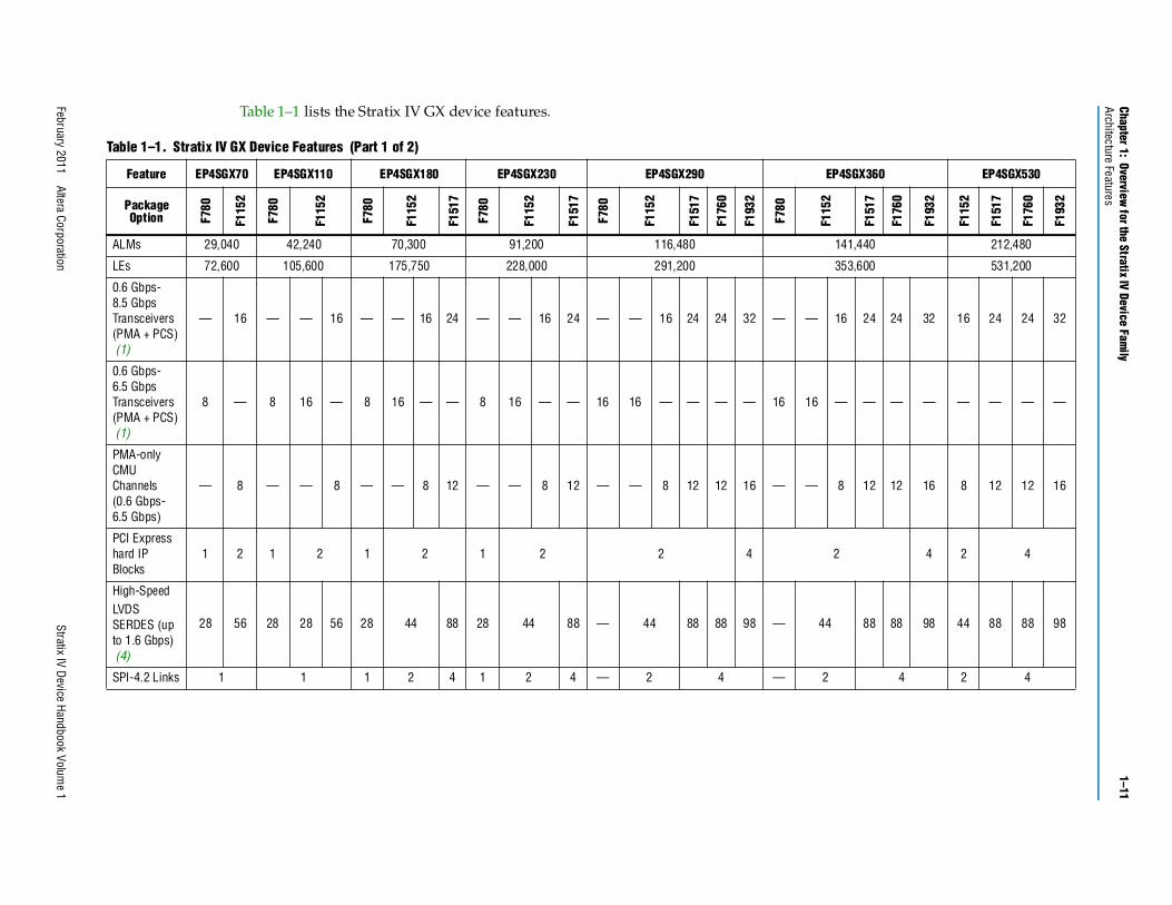
Table 1–1 lists the Stratix IV GX device features.
Table 1–1. Stratix IV GX Device Features (Part 1 of 2)
Feature EP4SGX70 EP4SGX110 EP4SGX180 EP4SGX230 EP4SGX290
Package Option F7
80
F115
2
F780
F115
2
F780
F115
2
F151
7
F780
F115
2
F151
7
F780
F115
2
F151
7
F176
0
F193
2
F780
ALMs 29,040 42,240 70,300 91,200 116,480
LEs 72,600 105,600 175,750 228,000 291,200
0.6 Gbps-8.5 Gbps Transceivers (PMA + PCS)(1)
— 16 — — 16 — — 16 24 — — 16 24 — — 16 24 24 32 — —
0.6 Gbps-6.5 Gbps Transceivers (PMA + PCS) (1)
8 — 8 16 — 8 16 — — 8 16 — — 16 16 — — — — 16 16
PMA-only CMU Channels (0.6 Gbps-6.5 Gbps)
— 8 — — 8 — — 8 12 — — 8 12 — — 8 12 12 16 — —
PCI Express hard IP Blocks
1 2 1 2 1 2 1 2 2 4
High-SpeedLVDS SERDES (up to 1.6 Gbps) (4)
28 56 28 28 56 28 44 88 28 44 88 — 44 88 88 98 —
SPI-4.2 Links 1 1 1 2 4 1 2 4 — 2 4 —
1–12Chapter 1:
Overview for the Stratix IV Device Family
Architecture Features
Stratix IV Device H
andbook Volume 1
February 2011Altera Corporation
1,248 1,280
48 64
22,564 27,376
1,0401,02
4 1,024
6 8 12 12 6 8 12 12
4 564
744
880
920 564 744 880 920
× ,
–2, –3, –4
–2, –3, –4
–2, –3, –4
–2, –3, –4
–2, –3, –4
–2, –3, –4
–2, –3, –4
–2, –3, –4
e devices have eight transceiver channels located only
and dedicated configuration pins are not included in
s you to use the transceiver CMU blocks as transceiver hannels in the Stratix IV GX –2x device, the data rates
EP4SGX360 EP4SGX530
F115
2
F151
7
F176
0
F193
2
F115
2
F151
7
F176
0
F193
2
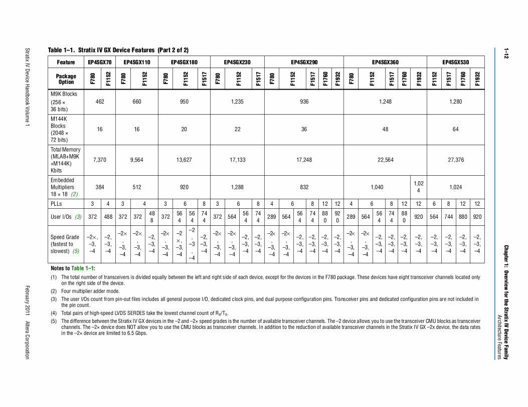
M9K Blocks(256 × 36 bits)
462 660 950 1,235 936
M144K Blocks(2048 × 72 bits)
16 16 20 22 36
Total Memory (MLAB+M9K+M144K) Kbits
7,370 9,564 13,627 17,133 17,248
Embedded Multipliers 18 × 18 (2)
384 512 920 1,288 832
PLLs 3 4 3 4 3 6 8 3 6 8 4 6 8 12 12 4
User I/Os (3) 372 488 372 372 488
372 564
564
744
372 564 564
744
289 564 564
744
880
920
289 56
Speed Grade (fastest to slowest) (5)
–2× , –3, –4
–2, –3, –4
–2×,
–3, –4
–2×,
–3, –4
–2, –3, –4
–2×,
–3, –4
–2× , –3, –4
–2,
–3,
–4
–2, –3, –4
–2×,
–3, –4
–2×,
–3, –4
–2, –3, –4
–2, –3, –4
–2×,
–3, –4
–2×,
–3, –4
–2, –3, –4
–2, –3, –4
–2, –3, –4
–2, –3, –4
–2×,
–3, –4
–2,
–3–4
Notes to Table 1–1:(1) The total number of transceivers is divided equally between the left and right side of each device, except for the devices in the F780 package. Thes
on the right side of the device.(2) Four multiplier adder mode.(3) The user I/Os count from pin-out files includes all general purpose I/O, dedicated clock pins, and dual purpose configuration pins. Transceiver pins
the pin count.(4) Total pairs of high-speed LVDS SERDES take the lowest channel count of RX/TX.(5) The difference between the Stratix IV GX devices in the –2 and –2× speed grades is the number of available transceiver channels. The –2 device allow
channels. The –2× device does NOT allow you to use the CMU blocks as transceiver channels. In addition to the reduction of available transceiver cin the –2× device are limited to 6.5 Gbps.
Table 1–1. Stratix IV GX Device Features (Part 2 of 2)
Feature EP4SGX70 EP4SGX110 EP4SGX180 EP4SGX230 EP4SGX290
Package Option F7
80
F115
2
F780
F115
2
F780
F115
2
F151
7
F780
F115
2
F151
7
F780
F115
2
F151
7
F176
0
F193
2
F780
Chapter 1:Overview for the Stratix IV Device Fam
ily1–13
Architecture Features
February 2011Altera Corporation
Stratix IV Device H
andbook Volume 1
satisfying the transient current devices accounts for the on-package
F17602.5 mm × 42.5 mm)
(6)
F1932(45 mm × 45 mm)
(6)
— —
— —
— —
— —
KF43 NF45
KF43 NF45
KF43 NF45
n Datasheet for Altera Devices.
ation about on-package decoupling capacitor value
Table 1–2 lists the Stratix IV GX device package options.
1 On-package decoupling reduces the need for on-board or PCB decoupling capacitors byrequirements at higher frequencies. The Power Delivery Network design tool for Stratix IVdecoupling and reflects the reduced requirements for PCB decoupling capacitors.
Table 1–2. Stratix IV GX Device Package Options (Note 1)
Device F780(29 mm × 29 mm) (5)
F1152(35 mm × 35 mm)
(5)
F1152(35 mm × 35 mm) (4), (6)
F1517(40 mm × 40 mm)
(4), (6)(4
EP4SGX70 DF29 — — HF35 — —
EP4SGX110 DF29 — FF35 HF35 — —
EP4SGX180 DF29 — FF35 — HF35 KF40
EP4SGX230 DF29 — FF35 — HF35 KF40
EP4SGX290 — FH29 (2) FF35 — HF35 KF40
EP4SGX360 — FH29 (2) FF35 — HF35 KF40
EP4SGX530 — — — — HH35 (3) KH40 (3)
Notes to Table 1–2:(1) Device packages in the same column and marked under the same arrow sign have vertical migration capability.(2) The 780-pin EP4SGX290 and EP4SGX360 devices are available only in 33 mm × 33 mm Hybrid flip chip package.(3) The 1152-pin and 1517-pin EP4SGX530 devices are available only in 42.5 mm × 42.5 mm Hybrid flip chip packages.(4) When migrating between hybrid and flip chip packages, there is an additional keep-out area. For more information, refer to the Package Informatio(5) Devices listed in this column are available in –2×, –3, and –4 speed grades. These devices do not have on-package decoupling capacitors.(6) Devices listed in this column are available in –2, –3, and –4 speed grades. These devices have on-package decoupling capacitors. For more inform
in each device, refer to Table 1–3.
1–14Chapter 1:
Overview for the Stratix IV Device Family
Architecture Features
Stratix IV Device H
andbook Volume 1
February 2011Altera Corporation
VCCA_L/R VCCT and VCCR (Shared)
100nF 1× 470nF + 1× 47nF per side
100nF 1× 470nF + 1× 47nF per side
100nF 1× 470nF + 1× 47nF per side
100 nF 1× 470 nF + 1× 47 nF per side
100nF 1× 470 nF + 1× 47 nF per side
100 nF 1× 470 nF + 1× 47 nF per side
100 nF 1× 470 nF + 1× 47 nF per side
, contact Altera Technical Support.
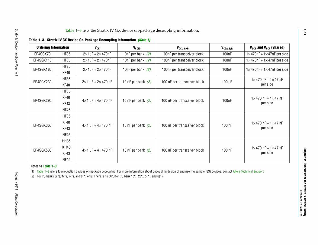
Table 1–3 lists the Stratix IV GX device on-package decoupling information.
Table 1–3. Stratix IV GX Device On-Package Decoupling Information (Note 1)
Ordering Information VCC VCCIO VCCL_GXB
EP4SGX70 HF35 2× 1uF + 2× 470nF 10nF per bank (2) 100nF per transceiver block
EP4SGX110 HF35 2× 1uF + 2× 470nF 10nF per bank (2) 100nF per transceiver block
EP4SGX180HF35
KF402× 1uF + 2× 470nF 10nF per bank (2) 100nF per transceiver block
EP4SGX230HF35
KF402× 1 uF + 2× 470 nF 10 nF per bank (2) 100 nF per transceiver block
EP4SGX290
HF35
KF40
KF43
NF45
4× 1 uF + 4× 470 nF 10 nF per bank (2) 100 nF per transceiver block
EP4SGX360
HF35
KF40
KF43
NF45
4× 1 uF + 4× 470 nF 10 nF per bank (2) 100 nF per transceiver block
EP4SGX530
HH35
KH40
KF43
NF45
4× 1 uF + 4× 470 nF 10 nF per bank (2) 100 nF per transceiver block
Notes to Table 1–3:(1) Table 1–3 refers to production devices on-package decoupling. For more information about decoupling design of engineering sample (ES) devices(2) For I/O banks 3(*), 4(*), 7(*), and 8(*) only. There is no OPD for I/O bank 1(*), 2(*), 5(*), and 6(*).
Chapter 1: Overview for the Stratix IV Device Family 1–15Architecture Features
0
(4)
4
ins
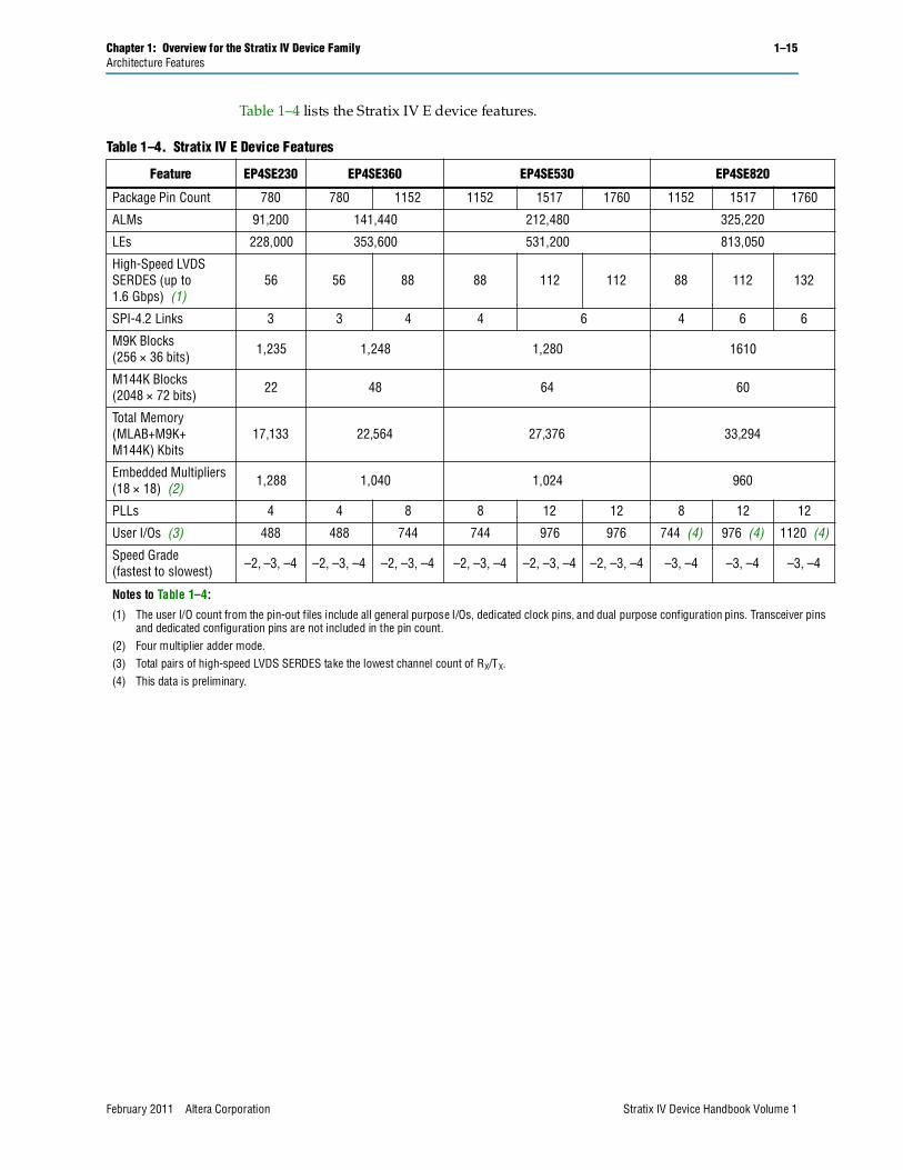
Table 1–4 lists the Stratix IV E device features.
Table 1–4. Stratix IV E Device Features
Feature EP4SE230 EP4SE360 EP4SE530 EP4SE820
Package Pin Count 780 780 1152 1152 1517 1760 1152 1517 176
ALMs 91,200 141,440 212,480 325,220
LEs 228,000 353,600 531,200 813,050
High-Speed LVDS SERDES (up to 1.6 Gbps) (1)
56 56 88 88 112 112 88 112 132
SPI-4.2 Links 3 3 4 4 6 4 6 6
M9K Blocks(256 × 36 bits) 1,235 1,248 1,280 1610
M144K Blocks(2048 × 72 bits) 22 48 64 60
Total Memory (MLAB+M9K+M144K) Kbits
17,133 22,564 27,376 33,294
Embedded Multipliers(18 × 18) (2) 1,288 1,040 1,024 960
PLLs 4 4 8 8 12 12 8 12 12
User I/Os (3) 488 488 744 744 976 976 744 (4) 976 (4) 1120
Speed Grade (fastest to slowest) –2, –3, –4 –2, –3, –4 –2, –3, –4 –2, –3, –4 –2, –3, –4 –2, –3, –4 –3, –4 –3, –4 –3, –
Notes to Table 1–4:
(1) The user I/O count from the pin-out files include all general purpose I/Os, dedicated clock pins, and dual purpose configuration pins. Transceiver pand dedicated configuration pins are not included in the pin count.
(2) Four multiplier adder mode.(3) Total pairs of high-speed LVDS SERDES take the lowest channel count of RX/TX.(4) This data is preliminary.
February 2011 Altera Corporation Stratix IV Device Handbook Volume 1
1–16 Chapter 1: Overview for the Stratix IV Device FamilyArchitecture Features
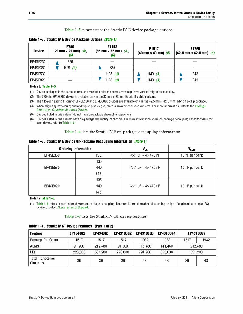
Table 1–5 summarizes the Stratix IV E device package options.
Table 1–6 lists the Stratix IV E on-package decoupling information.
Table 1–7 lists the Stratix IV GT device features.
Table 1–5. Stratix IV E Device Package Options (Note 1)
DeviceF780
(29 mm × 29 mm) (4), (5)
F1152 (35 mm × 35 mm) (4),
(6)
F1517 (40 mm × 40 mm) (6)
F1760 (42.5 mm × 42.5 mm) (6)
EP4SE230 F29 — — —
EP4SE360 H29 (2) F35 — —
EP4SE530 — H35 (3) H40 (3) F43
EP4SE820 — H35 (3) H40 (3) F43
Notes to Table 1–5:
(1) Device packages in the same column and marked under the same arrow sign have vertical migration capability.(2) The 780-pin EP4SE360 device is available only in the 33 mm × 33 mm Hybrid flip chip package.(3) The 1152-pin and 1517-pin for EP4SE530 and EP4SE820 devices are available only in the 42.5 mm × 42.5 mm Hybrid flip chip package.(4) When migrating between hybrid and flip chip packages, there is an additional keep-out area. For more information, refer to the Package
Information Datasheet for Altera Devices.(5) Devices listed in this column do not have on-package decoupling capacitors.(6) Devices listed in this column have on-package decoupling capacitors. For more information about on-package decoupling capacitor value for
each device, refer to Table 1–6.
Table 1–6. Stratix IV E Device On-Package Decoupling Information (Note 1)
Ordering Information VCC VCCIO
EP4SE360 F35 4× 1 uF + 4× 470 nF 10 nF per bank
EP4SE530
H35
H40
F43
4× 1 uF + 4× 470 nF 10 nF per bank
EP4SE820
H35
H40
F43
4× 1 uF + 4× 470 nF 10 nF per bank
Note to Table 1–6:
(1) Table 1–6 refers to production devices on-package decoupling. For more information about decoupling design of engineering sample (ES) devices, contact Altera Technical Support.
Table 1–7. Stratix IV GT Device Features (Part 1 of 2)
Feature EP4S40G2 EP4S40G5 EP4S100G2 EP4S100G3 EP4S100G4 EP4S100G5
Package Pin Count 1517 1517 1517 1932 1932 1517 1932
ALMs 91,200 212,480 91,200 116,480 141,440 212,480
LEs 228,000 531,200 228,000 291,200 353,600 531,200
Total Transceiver Channels
36 36 36 48 48 36 48
Stratix IV Device Handbook Volume 1 February 2011 Altera Corporation
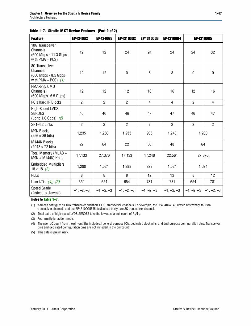
Chapter 1: Overview for the Stratix IV Device Family 1–17Architecture Features
10G Transceiver Channels(600 Mbps - 11.3 Gbps with PMA + PCS)
12 12 24 24 24 24 32
8G Transceiver Channels(600 Mbps - 8.5 Gbps with PMA + PCS) (1)
12 12 0 8 8 0 0
PMA-only CMU Channels (600 Mbps- 6.5 Gbps)
12 12 12 16 16 12 16
PCIe hard IP Blocks 2 2 2 4 4 2 4
High-Speed LVDS SERDES(up to 1.6 Gbps) (2)
46 46 46 47 47 46 47
SP1-4.2 Links 2 2 2 2 2 2 2
M9K Blocks(256 × 36 bits)
1,235 1,280 1,235 936 1,248 1,280
M144K Blocks(2048 × 72 bits)
22 64 22 36 48 64
Total Memory (MLAB + M9K + M144K) Kbits
17,133 27,376 17,133 17,248 22,564 27,376
Embedded Multipliers 18 × 18 (3)
1,288 1,024 1,288 832 1,024 1,024
PLLs 8 8 8 12 12 8 12
User I/Os (4), (5) 654 654 654 781 781 654 781
Speed Grade(fastest to slowest)
–1, –2, –3 –1, –2, –3 –1, –2, –3 –1, –2, –3 –1, –2, –3 –1, –2, –3 –1, –2, –3
Notes to Table 1–7:
(1) You can configure all 10G transceiver channels as 8G transceiver channels. For example, the EP4S40G2F40 device has twenty-four 8G transceiver channels and the EP4S100G5F45 device has thirty-two 8G transceiver channels.
(2) Total pairs of high-speed LVDS SERDES take the lowest channel count of RX/TX.(3) Four multiplier adder mode.(4) The user I/O count from the pin-out files include all general purpose I/Os, dedicated clock pins, and dual purpose configuration pins. Transceiver
pins and dedicated configuration pins are not included in the pin count.(5) This data is preliminary.
Table 1–7. Stratix IV GT Device Features (Part 2 of 2)
Feature EP4S40G2 EP4S40G5 EP4S100G2 EP4S100G3 EP4S100G4 EP4S100G5
February 2011 Altera Corporation Stratix IV Device Handbook Volume 1
1–18 Chapter 1: Overview for the Stratix IV Device FamilyArchitecture Features
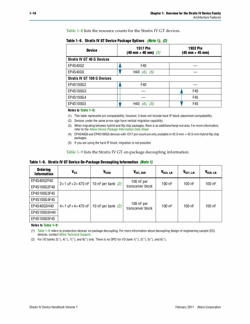
Table 1–8 lists the resource counts for the Stratix IV GT devices.
Table 1–9 lists the Stratix IV GT on-package decoupling information.
Table 1–8. Stratix IV GT Device Package Options (Note 1), (2)
Device 1517 Pin(40 mm × 40 mm) (3)
1932 Pin(45 mm × 45 mm)
Stratix IV GT 40 G Devices
EP4S40G2 F40 —
EP4S40G5 H40 (4), (5) —
Stratix IV GT 100 G Devices
EP4S100G2 F40 —
EP4S100G3 — F45
EP4S100G4 — F45
EP4S100G5 H40 (4), (5) F45
Notes to Table 1–8:
(1) This table represents pin compatability; however, it does not include hard IP block placement compatability.(2) Devices under the same arrow sign have vertical migration capability.(3) When migrating between hybrid and flip chip packages, there is an additional keep-out area. For more information,
refer to the Altera Device Package Information Data Sheet.(4) EP4S40G5 and EP4S100G5 devices with 1517 pin-count are only available in 42.5-mm × 42.5-mm Hybrid flip chip
packages.(5) If you are using the hard IP block, migration is not possible.
Table 1–9. Stratix IV GT Device On-Package Decoupling Information (Note 1)
Ordering Information VCC VCCIO VCCL_GXB VCCA_L/R VCCT_L/R VCCR_L/R
EP4S40G2F40
EP4S100G2F402× 1 uF + 2× 470 nF 10 nF per bank (2) 100 nF per
transceiver block100 nF 100 nF 100 nF
EP4S100G3F45
4× 1 uF + 4× 470 nF 10 nF per bank (2)100 nF per
transceiver block 100 nF 100 nF 100 nF
EP4S100G4F45
EP4S40G5H40
EP4S100G5H40
EP4S100G5F45
Notes to Table 1–9:
(1) Table 1–9 refers to production devices on-package decoupling. For more information about decoupling design of engineering sample (ES) devices, contact Altera Technical Support.
(2) For I/O banks 3(*), 4(*), 7(*), and 8(*) only. There is no OPD for I/O bank 1(*), 2(*), 5(*), and 6(*).
Stratix IV Device Handbook Volume 1 February 2011 Altera Corporation
Chapter 1: Overview for the Stratix IV Device Family 1–19Integrated Software Platform
Integrated Software PlatformThe Quartus II software provides an integrated environment for HDL and schematic design entry, compilation and logic synthesis, full simulation and advanced timing analysis, SignalTap II Logic Analyzer, and device configuration of Stratix IV designs. The Quartus II software provides the MegaWizard™ Plug-In Manager user interface to generate different functional blocks, such as memory, PLL, and digital signal processing logic. For transceivers, the Quartus II software provides the ALTGX MegaWizard Plug-In Manager interface that guides you through configuration of the transceiver based on your application requirements.
The Stratix IV GX and GT transceivers allow you to implement low-power and reliable high-speed serial interface applications with its fully reconfigurable hardware, optimal signal integrity, and integrated Quartus II software platform.
f For more information about the Quartus II software features, refer to the Quartus II Handbook.
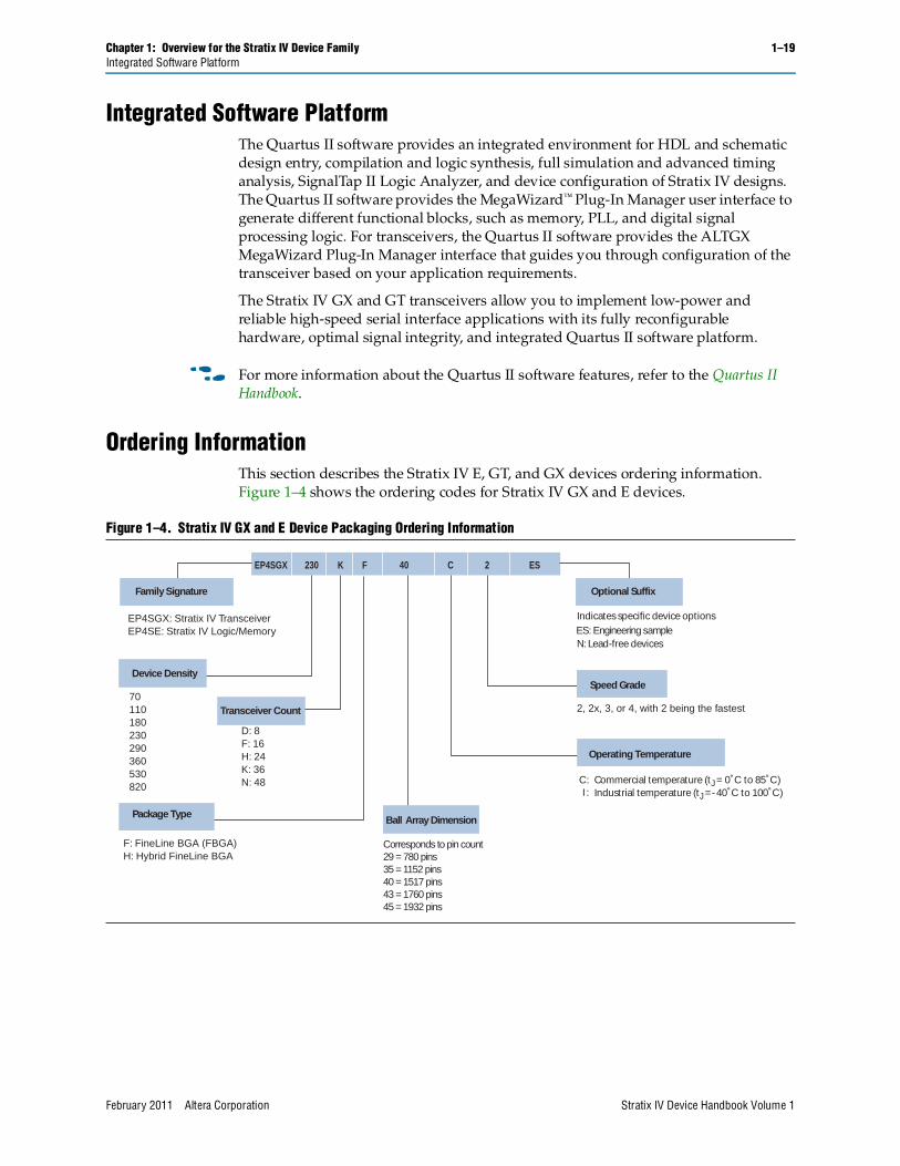
Ordering InformationThis section describes the Stratix IV E, GT, and GX devices ordering information. Figure 1–4 shows the ordering codes for Stratix IV GX and E devices.
Figure 1–4. Stratix IV GX and E Device Packaging Ordering Information
Device Density
Transceiver Count
Package Type
2, 2x, 3, or 4, with 2 being the fastest
Corresponds to pin count29 = 780 pins35 = 1152 pins40 = 1517 pins43 = 1760 pins45 = 1932 pins
F: FineLine BGA (FBGA)H: Hybrid FineLine BGA
EP4SGX: Stratix IV Transceiver
D: 8F: 16H: 24K: 36N: 48
EP4SE: Stratix IV Logic/Memory
70110180230290360530820
C: Commercial temperature (tJ= 0 C to 85 C)Industrial temperature (tJ=-40 C to 100 C)
Optional SuffixFamilyS i g n a t u r e
Operating Temperature
Speed Grade
Ball Array Dimension
2EP4SGX 230 C40FK ES
Indicatesspecific device options
N:Lead-free devices
I :
ES: Engineering sample
February 2011 Altera Corporation Stratix IV Device Handbook Volume 1
1–20 Chapter 1: Overview for the Stratix IV Device FamilyDocument Revision History
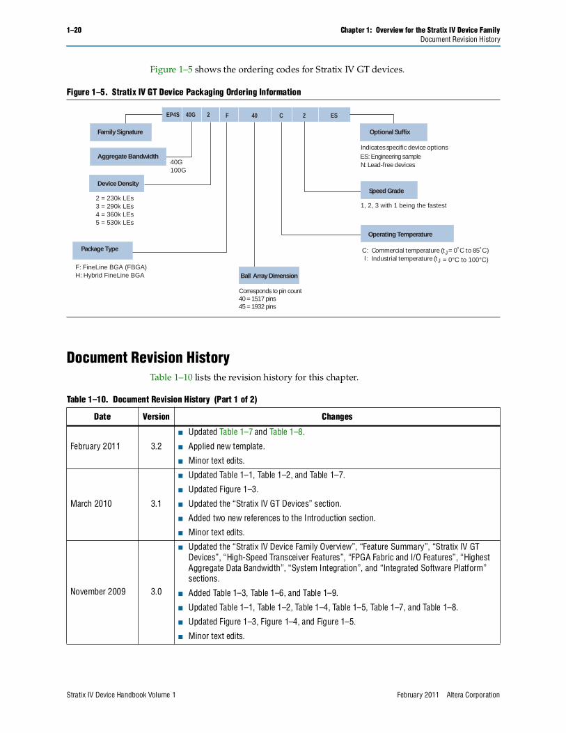
Figure 1–5 shows the ordering codes for Stratix IV GT devices.
Document Revision HistoryTable 1–10 lists the revision history for this chapter.
Figure 1–5. Stratix IV GT Device Packaging Ordering Information
Device Density
Package Type
1, 2, 3 with 1 being the fastest
Corresponds to pin count40 = 1517 pins45 = 1932 pins
F: FineLine BGA (FBGA)H: Hybrid FineLine BGA
2 = 230k LEs3 = 290k LEs4 = 360k LEs5 = 530k LEs
C: Commercial temperature (tJ= 0 C to 85 C)Industrial temperature (tJ = 0°C to 100°C)
Optional SuffixFamilyS i g n a t u r e
Operating Temperature
Speed Grade
Ball Array Dimension
2EP4S 230 C40F ES
Indicatesspecific device options
N:Lead-free devices
I :
ES: Engineering sample Aggregate Bandwidth
EP4S 240G
40G100G
Table 1–10. Document Revision History (Part 1 of 2)
Date Version Changes
February 2011 3.2
■ Updated Table 1–7 and Table 1–8.
■ Applied new template.
■ Minor text edits.
March 2010 3.1
■ Updated Table 1–1, Table 1–2, and Table 1–7.
■ Updated Figure 1–3.
■ Updated the “Stratix IV GT Devices” section.
■ Added two new references to the Introduction section.
■ Minor text edits.
November 2009 3.0
■ Updated the “Stratix IV Device Family Overview”, “Feature Summary”, “Stratix IV GT Devices”, “High-Speed Transceiver Features”, “FPGA Fabric and I/O Features”, “Highest Aggregate Data Bandwidth”, “System Integration”, and “Integrated Software Platform” sections.
■ Added Table 1–3, Table 1–6, and Table 1–9.
■ Updated Table 1–1, Table 1–2, Table 1–4, Table 1–5, Table 1–7, and Table 1–8.
■ Updated Figure 1–3, Figure 1–4, and Figure 1–5.
■ Minor text edits.
Stratix IV Device Handbook Volume 1 February 2011 Altera Corporation
Chapter 1: Overview for the Stratix IV Device Family 1–21Document Revision History
June 2009 2.4■ Updated Table 1–1.
■ Minor text edits.
April 2009 2.3
■ Added Table 1–5, Table 1–6, and Figure 1–3.
■ Updated Figure 1–5.
■ Updated Table 1–1, Table 1–2, Table 1–3, and Table 1–4.
■ Updated “Introduction”, “Feature Summary”, “Stratix IV GX Devices”, “Stratix IV GT Devices”, “Architecture Features”, and “FPGA Fabric and I/O Features”
March 2009 2.2
■ Updated “Feature Summary”, “Stratix IV GX Devices”, “Stratix IV E Device”, “Stratix IV GT Devices”, “Signal Integrity”
■ Removed Tables 1-5 and 1-6
■ Updated Figure 1–4
March 2009 2.1
■ Updated “Introduction”, “Feature Summary”, “Stratix IV Device Diagnostic Features”, “Signal Integrity”, “Clock Networks”,“High-Speed Differential I/O with DPA and Soft-CDR”, “System Integration”, and “Ordering Information” sections.
■ Added “Stratix IV GT 100G Devices” and “Stratix IV GT 100G Transceiver Bandwidth” sections.
■ Updated Table 1–1, Table 1–2, Table 1–3, and Table 1–4.
■ Added Table 1–5 and Table 1–6.
■ Updated Figure 1–3 and Figure 1–4.
■ Added Figure 1–5.
■ Removed “Referenced Documents” section.
November 2008 2.0
■ Updated “Feature Summary” on page 1–1.
■ Updated “Stratix IV Device Diagnostic Features” on page 1–7.
■ Updated “FPGA Fabric and I/O Features” on page 1–8.
■ Updated Table 1–1.
■ Updated Table 1–2.
■ Updated “Table 1–5 shows the total number of transceivers available in the Stratix IV GT Device.” on page 1–15.
July 2008 1.1 Revised “Introduction”.
May 2008 1.0 Initial release.
Table 1–10. Document Revision History (Part 2 of 2)
Date Version Changes
February 2011 Altera Corporation Stratix IV Device Handbook Volume 1
1–22 Chapter 1: Overview for the Stratix IV Device FamilyDocument Revision History
Stratix IV Device Handbook Volume 1 February 2011 Altera Corporation