Embed Size (px)
Citation preview
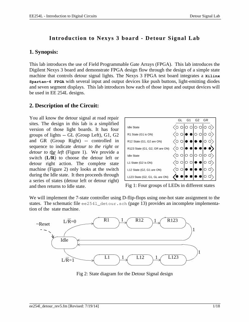
EE254L - Introduction to Digital Circuits Detour Signal Lab
ee254l_detour_rev5.fm [Revised: 7/19/14] 1/18
Introduct ion to Nexys 3 board - Detour S ignal Lab
1. Synopsis:
This lab introduces the use of Field Programmable Gate Arrays (FPGA). This lab introduces theDigilent Nexys 3 board and demonstrate FPGA design flow through the design of a simple statemachine that controls detour signal lights. The Nexys 3 FPGA test board integrates a XilinxSpartan-6 FPGA with several input and output devices like push buttons, light-emitting diodesand seven segment displays. This lab introduces how each of those input and output devices willbe used in EE 254L designs.
2. Description of the Circuit:
You all know the detour signal at road repairsites. The design in this lab is a simplifiedversion of those light boards. It has fourgroups of lights -- GL (Group Left), G1, G2and GR (Group Right) -- controlled insequence to indicate detour to the right ordetour to the left (Figure 1). We provide aswitch (L/R) to choose the detour left ordetour right action. The complete statemachine (Figure 2) only looks at the switchduring the Idle state. It then proceeds througha series of states (detour left or detour right)and then returns to Idle state.
We will implement the 7-state controller using D-flip-flops using one-hot state assignment to thestates. The schematic file ee254l_detour.sch (page 13) provides an incomplete implementa-tion of the state machine.
Fig 1: Four groups of LEDs in different states
Idle State
R1 State (G1 is ON)
R12 State (G1, G2 are ON)
R123 State (G1, G2, GR are ON)
Idle State
L1 State (G2 is ON)
L12 State (G2, G1 are ON)
L123 State (G2, G1, GL are ON)
GL G1 G2 GR
R1 R12 R123
L123L12L1
Idle
L/R=0
L/R=1
~Reset
Fig 2: State diagram for the Detour Signal design
1 1
1 11
1
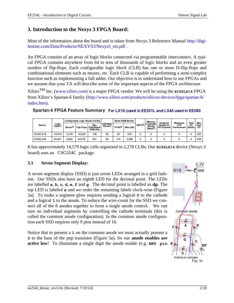
EE254L - Introduction to Digital Circuits Detour Signal Lab
ee254l_detour_rev5.fm [Revised: 7/19/14] 2/18
3. Introduction to the Nexys 3 FPGA Board:
Most of the information about the board and is taken from Nexys 3 Reference Manual http://digi-lentinc.com/Data/Products/NEXYS3/Nexys3_rm.pdf .
An FPGA consists of an array of logic blocks connected via programmable interconnect. A typi-cal FPGA contains anywhere from 64 to tens of thousands of logic blocks and an even greaternumber of flip-flops. Each configurable logic block (CLB) has one or more D-flip-flops andcombinational elements such as muxes, etc. Each CLB is capable of performing a semi-complexfunction such as implementing a full adder. Our objective is to understand how to use FPGAs andwe assume that your TA will describe some of the important aspects of the FPGA architectureXilinxTM Inc. (www.xilinx.com) is a major FPGA vendor. We will be using the XC6SLX16 FPGA from Xilinx’s Spartan-6 family (http://www.xilinx.com/products/silicon-devices/fpga/spartan-6/index.htm).
It has approximately 14,579 logic cells organized in 2,278 CLBs. Our XC6SLX16 device (Nexys 3 board) uses an CSG324C package.
3.1 Seven Segment Display:
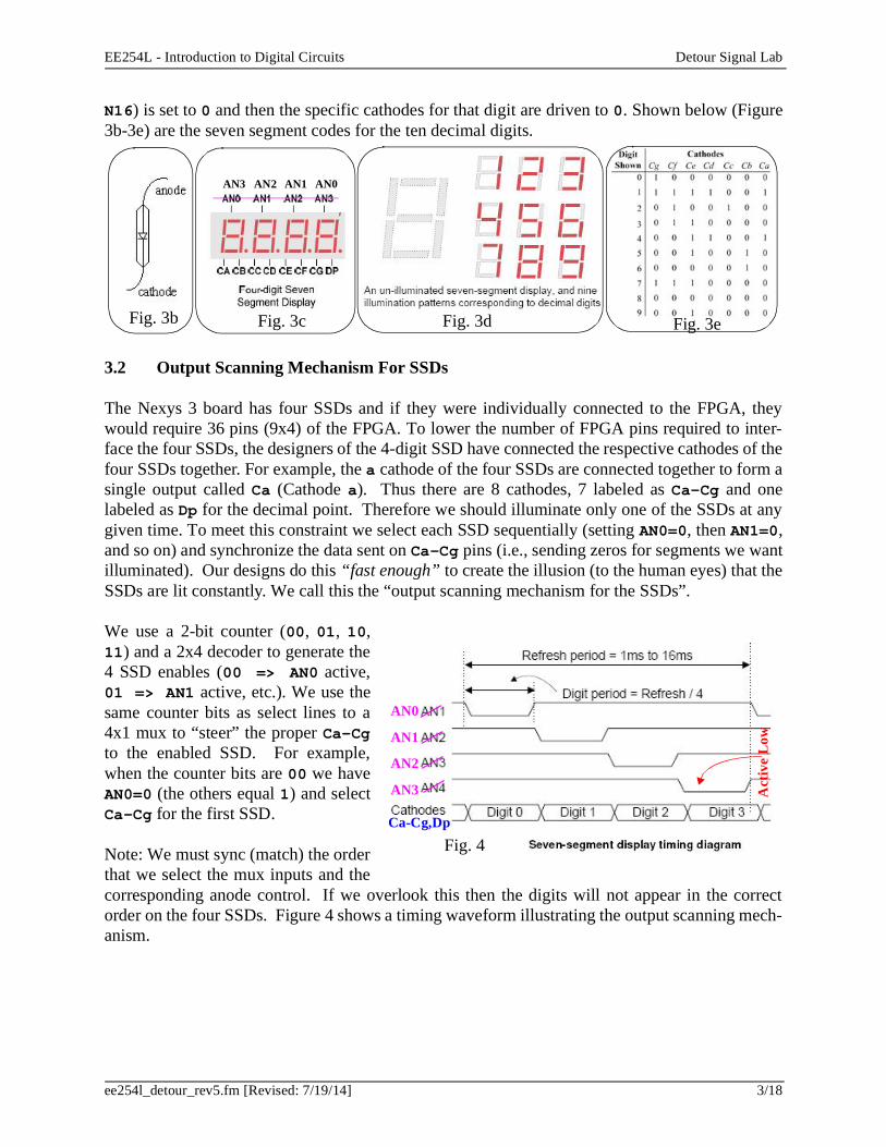
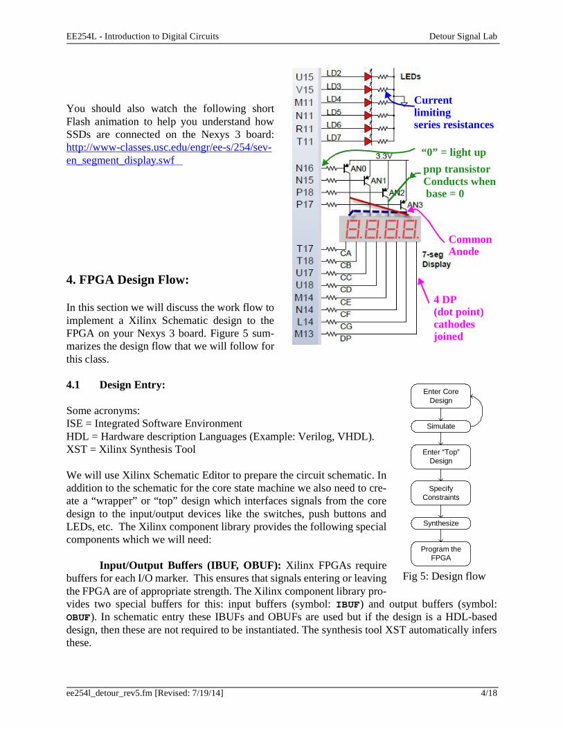
A seven segment display (SSD) is just seven LEDs arranged in a grid fash-ion. Our SSDs also have an eighth LED for the decimal point. The LEDsare labelled a, b, c, d, e, f and g. The decimal point is labelled as dp. Thetop LED is labeled a and we order the remaining labels clock-wise (Figure3a). To make a segment glow requires sending a logical 0 to the cathodeand a logical 1 to the anode. To reduce the wire-count for the SSD we con-nect all of the 8 anodes together to form a single anode control. We canturn on individual segments by controlling the cathode terminals (this iscalled the common anode configuration). In the common anode configura-tion each SSD requires only 9 pins instead of 16.
Notice that to present a 1 on the common anode we must actually present a0 to the base of the pnp transistor (Figure 3a). So our anode enables areactive low! To illuminate a single digit the anode enable (e.g. AN0 pin
3.3V
1
0
Fig. 3a
EE254L - Introduction to Digital Circuits Detour Signal Lab
ee254l_detour_rev5.fm [Revised: 7/19/14] 3/18
N16) is set to 0 and then the specific cathodes for that digit are driven to 0. Shown below (Figure3b-3e) are the seven segment codes for the ten decimal digits.
3.2 Output Scanning Mechanism For SSDs
The Nexys 3 board has four SSDs and if they were individually connected to the FPGA, theywould require 36 pins (9x4) of the FPGA. To lower the number of FPGA pins required to inter-face the four SSDs, the designers of the 4-digit SSD have connected the respective cathodes of thefour SSDs together. For example, the a cathode of the four SSDs are connected together to form asingle output called Ca (Cathode a). Thus there are 8 cathodes, 7 labeled as Ca-Cg and onelabeled as Dp for the decimal point. Therefore we should illuminate only one of the SSDs at anygiven time. To meet this constraint we select each SSD sequentially (setting AN0=0, then AN1=0,and so on) and synchronize the data sent on Ca-Cg pins (i.e., sending zeros for segments we wantilluminated). Our designs do this “fast enough” to create the illusion (to the human eyes) that theSSDs are lit constantly. We call this the “output scanning mechanism for the SSDs”.
We use a 2-bit counter (00, 01, 10,11) and a 2x4 decoder to generate the4 SSD enables (00 => AN0 active,01 => AN1 active, etc.). We use thesame counter bits as select lines to a4x1 mux to “steer” the proper Ca-Cgto the enabled SSD. For example,when the counter bits are 00 we haveAN0=0 (the others equal 1) and selectCa-Cg for the first SSD.
Note: We must sync (match) the orderthat we select the mux inputs and thecorresponding anode control. If we overlook this then the digits will not appear in the correctorder on the four SSDs. Figure 4 shows a timing waveform illustrating the output scanning mech-anism.
AN3 AN2 AN0AN1
Fig. 3cFig. 3b Fig. 3d Fig. 3e
AN0
AN1
AN2
AN3
Ca-Cg,Dp
Fig. 4
Act
ive
Low
EE254L - Introduction to Digital Circuits Detour Signal Lab
ee254l_detour_rev5.fm [Revised: 7/19/14] 4/18
You should also watch the following shortFlash animation to help you understand howSSDs are connected on the Nexys 3 board:http://www-classes.usc.edu/engr/ee-s/254/sev-en_segment_display.swf
4. FPGA Design Flow:
In this section we will discuss the work flow toimplement a Xilinx Schematic design to theFPGA on your Nexys 3 board. Figure 5 sum-marizes the design flow that we will follow forthis class.
4.1 Design Entry:
Some acronyms:ISE = Integrated Software EnvironmentHDL = Hardware description Languages (Example: Verilog, VHDL).XST = Xilinx Synthesis Tool
We will use Xilinx Schematic Editor to prepare the circuit schematic. Inaddition to the schematic for the core state machine we also need to cre-ate a “wrapper” or “top” design which interfaces signals from the coredesign to the input/output devices like the switches, push buttons andLEDs, etc. The Xilinx component library provides the following specialcomponents which we will need:
Input/Output Buffers (IBUF, OBUF): Xilinx FPGAs requirebuffers for each I/O marker. This ensures that signals entering or leavingthe FPGA are of appropriate strength. The Xilinx component library pro-vides two special buffers for this: input buffers (symbol: IBUF) and output buffers (symbol:OBUF). In schematic entry these IBUFs and OBUFs are used but if the design is a HDL-baseddesign, then these are not required to be instantiated. The synthesis tool XST automatically infersthese.
Current limitingseries resistances
pnp transistorConducts when base = 0
“0” = light up
CommonAnode
4 DP (dot point)cathodesjoined
Fig 5: Design flow
Enter Core Design
Simulate
Specify Constraints
Enter “Top” Design
Synthesize
Program the FPGA
EE254L - Introduction to Digital Circuits Detour Signal Lab
ee254l_detour_rev5.fm [Revised: 7/19/14] 5/18
Global Buffers (BUFGP): Xilinx FPGAs also have special buffers called “Global Pri-mary Buffers” (symbol: BUFGP). We must use these buffer for certain incoming signals likeclock which have “high fan-out”. For example, after the input marker for the clock pin you mustplace a global buffer (BUFGP). Only then can you send the clock to your circuit elements likeflips-flops, counters, etc. You cannot use general purpose buffers (symbol: BUF) or input buffers(IBUF) for the clock signal!
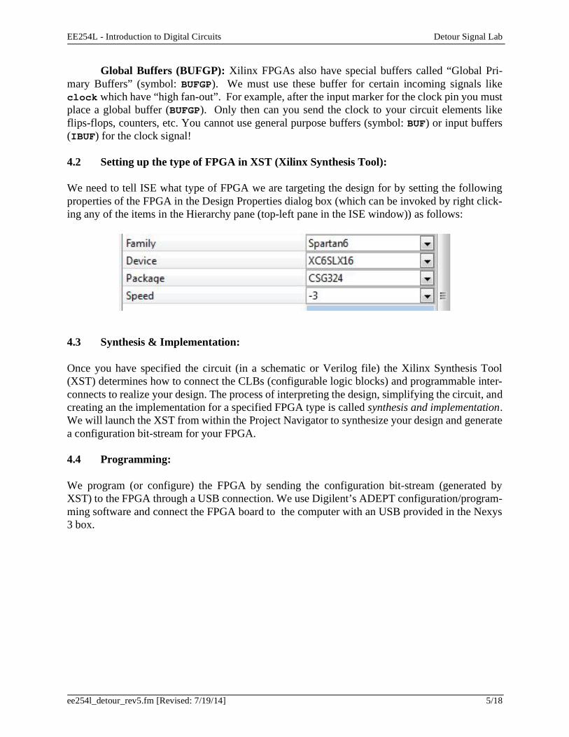
4.2 Setting up the type of FPGA in XST (Xilinx Synthesis Tool):
We need to tell ISE what type of FPGA we are targeting the design for by setting the followingproperties of the FPGA in the Design Properties dialog box (which can be invoked by right click-ing any of the items in the Hierarchy pane (top-left pane in the ISE window)) as follows:
4.3 Synthesis & Implementation:
Once you have specified the circuit (in a schematic or Verilog file) the Xilinx Synthesis Tool(XST) determines how to connect the CLBs (configurable logic blocks) and programmable inter-connects to realize your design. The process of interpreting the design, simplifying the circuit, andcreating an the implementation for a specified FPGA type is called synthesis and implementation.We will launch the XST from within the Project Navigator to synthesize your design and generatea configuration bit-stream for your FPGA.
4.4 Programming:
We program (or configure) the FPGA by sending the configuration bit-stream (generated byXST) to the FPGA through a USB connection. We use Digilent’s ADEPT configuration/program-ming software and connect the FPGA board to the computer with an USB provided in the Nexys3 box.

EE254L - Introduction to Digital Circuits Detour Signal Lab
ee254l_detour_rev5.fm [Revised: 7/19/14] 6/18
5. Prelab:
Q 5. 1: What does “FPGA” stand for? (1pt)
Q 5. 2: What is the name of the FPGA family that we are using in this lab? (1pt)
Q 5. 3: Which FPGA of this family are we using? (1pt)
Q 5. 4: What does CSG324 denote in the design properties dialog box? (1pt)
Speed grade Package Serial number Model number
Q 5. 5: The state memory is usually implemented using: (2pts)
And-Or gates RAM flip-flops All of the above
Q 5. 6: Next State Logic (NSL) is a purely ______________________________________ (combinational/sequential) circuit. (2pts)
Q 5. 7: We will implement the detour signal controller using One-Hot state assignment method. How many D-flip-flops are needed to implement the controller? (2pts)
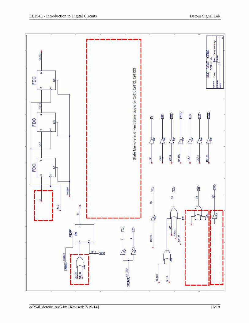
Q 5. 8: In the schematic ee254l_detour.sch (on page 16), next state logic for which state(s) is complete? (2pts)
Q 5. 9: Name the 3 components you need to construct the output scanning mechanism. Be sure to include bus-widths and input-output counts. (3pts)
EE254L - Introduction to Digital Circuits Detour Signal Lab
ee254l_detour_rev5.fm [Revised: 7/19/14] 7/18
6. Procedure:
6.1 Download the zip file ee254l_detour_Nexys3_EXER.zip containing the Xilinx ISE proj-ect from the Blackboard. Extract the zipped project folder ee254l_detour_Nexys3_EXER intothe projects folder (C:\Xilinx_projects\). Open the project in Xilinx ISE. We provide incom-plete schematic files which you will complete, simulate, synthesize/implement and finally down-load to your FPGA board. To help you, the incomplete/incorrect portions of the schematic are identified by dashed cir-
cles or rectangles .
We divide the design into two major parts: the CORE design and the TOP design (refer to section4.1). The core design solves the particular problem/task (usually involving a DPU (data path unit)and a CU (control unit)). We generally simulate and debug the core design separately by using acore test bench. Once you are satisfied with your core design you can use the symbol wizard andcreate a symbol for our core design. You can then incorporate your core by instantiating that inthe top design. The top-design focuses on interfacing the FPGA’s I/O resources (push-buttons,switches, LEDs, and SSDs) to the core design. You can then implement the design and downloadthe bit file to the board and verify the operation of the system we built. NOTE: We do not usu-ally write test benches for the top-design!
Part 1: Completing the core design
6.2 Open the ee254l_detour.sch schematic file. This is an incomplete implementation ofthe state machine. Complete the design by adding additional state memory (flip-flops), next statelogic, and output function logic. Notice the two different types of flip-flops used -- FDP and FDC.Determine the difference between them using the “Symbol Info” button in the schematic editor’s“Symbols” tab. Your completed design must implement the state machine in Figure 2 and thenproduce the four output signals (OFL): GL, G1, G2 and GR.
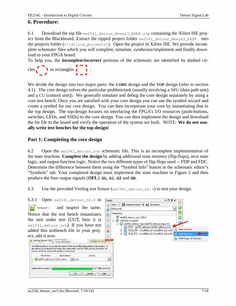
6.3 Use the provided Verilog test fixture (ee254l_detour_tb.v) to test your design.
6.3.1 Open ee254l_detour_tb.v in
and inspect the same.Notice that the test bench instantiatesthe unit under test (UUT, here it isee254l_detour.sch). If you have notadded this testbench file to your proj-ect, add it now.
EE254L - Introduction to Digital Circuits Detour Signal Lab
ee254l_detour_rev5.fm [Revised: 7/19/14] 8/18
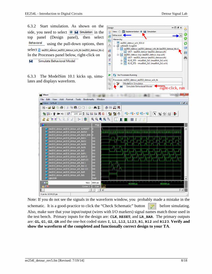
6.3.2 Start simulation. As shown on theside, you need to select in thetop panel (Design panel), then select
using the pull-down options, thenselect In the Processes panel below, right-click on
6.3.3 The ModelSim 10.1 kicks up, simu-lates and displays waveform.
Note: If you do not see the signals in the waveform window, you probably made a mistake in theschematic. It is a good-practice to click the “Check Schematic” button before simulating.Also, make sure that your input/output (wires with I/O markers) signal names match those used inthe test bench. Primary inputs for the design are: CLK, RESET, and LR_BAR. The primary outputsare: GL, G1, G2, GR and the one-hot coded states I, L1, L12, L123, R1, R12 and R123. Verify andshow the waveform of the completed and functionally correct design to your TA.
right-click, run
EE254L - Introduction to Digital Circuits Detour Signal Lab
ee254l_detour_rev5.fm [Revised: 7/19/14] 9/18
Part 2: Completing a simple “top” design
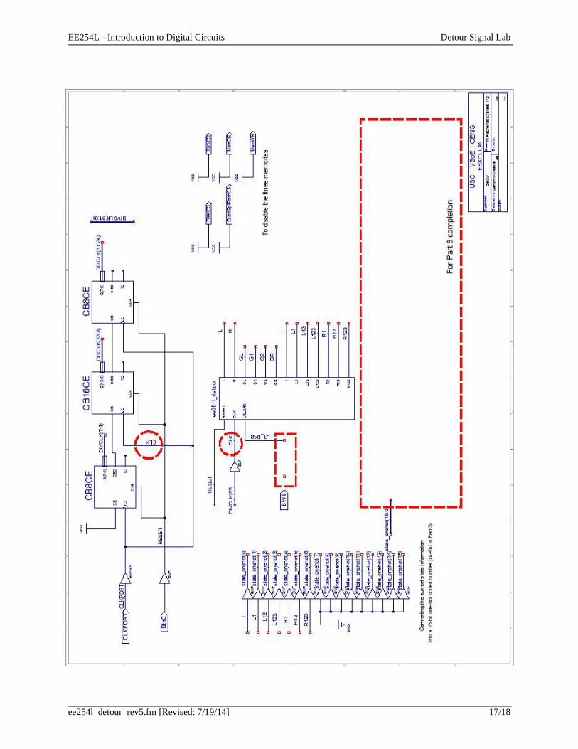
In part 2 our goal is to implement your detour design onto the FPGA board. You will design asimple “top” schematic that wraps your Part 1 state machine and interfaces its inputs and outputsto the FPGA board. You should not change your core state machine in this Part. You will placeall the necessary logic (called “glue logic”) in the “top” file.
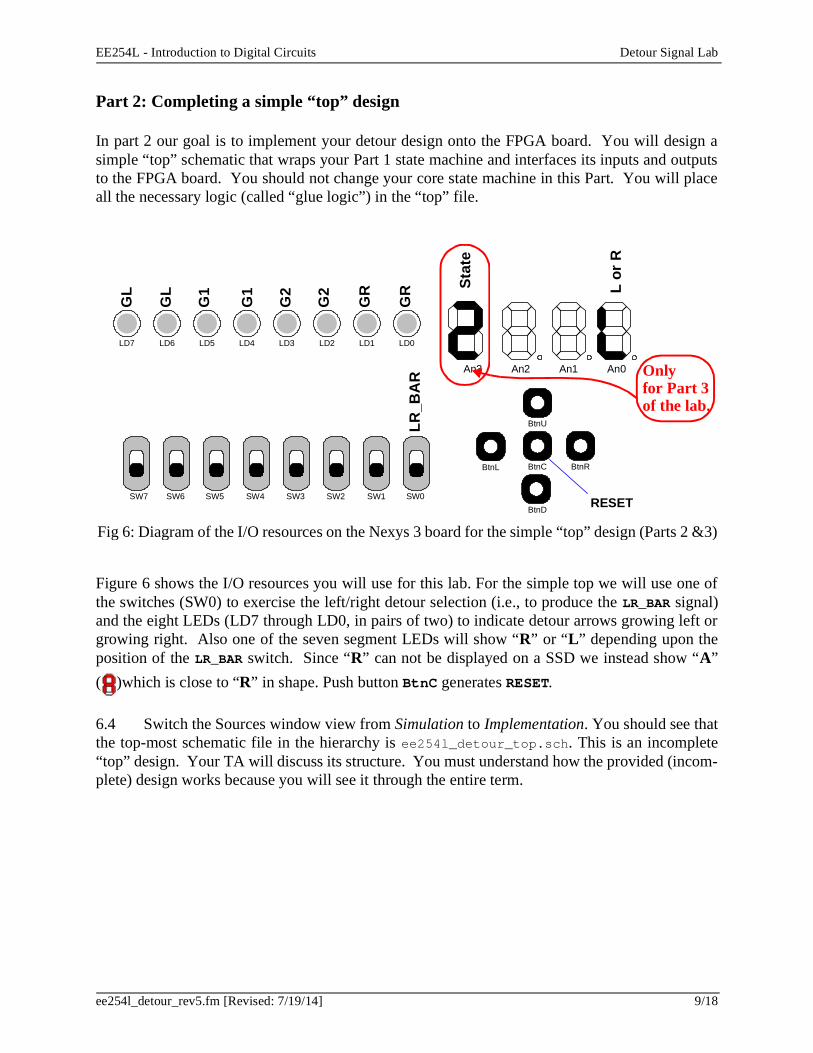
Figure 6 shows the I/O resources you will use for this lab. For the simple top we will use one ofthe switches (SW0) to exercise the left/right detour selection (i.e., to produce the LR_BAR signal)and the eight LEDs (LD7 through LD0, in pairs of two) to indicate detour arrows growing left orgrowing right. Also one of the seven segment LEDs will show “R” or “L” depending upon theposition of the LR_BAR switch. Since “R” can not be displayed on a SSD we instead show “A”( )which is close to “R” in shape. Push button BtnC generates RESET.
6.4 Switch the Sources window view from Simulation to Implementation. You should see thatthe top-most schematic file in the hierarchy is ee254l_detour_top.sch. This is an incomplete“top” design. Your TA will discuss its structure. You must understand how the provided (incom-plete) design works because you will see it through the entire term.
An3 An2 An1 An0
L or
R
Stat
eBtnC
BtnU
BtnRBtnL
BtnD RESETSW7 SW6 SW5 SW4 SW3 SW2 SW1 SW0
LR_B
AR
LD7 LD6 LD5 LD4 LD3 LD2 LD1 LD0
GL
GL
G1
G1
G2
G2
GR
GR
Fig 6: Diagram of the I/O resources on the Nexys 3 board for the simple “top” design (Parts 2 &3)
Onlyfor Part 3of the lab.
EE254L - Introduction to Digital Circuits Detour Signal Lab
ee254l_detour_rev5.fm [Revised: 7/19/14] 10/18
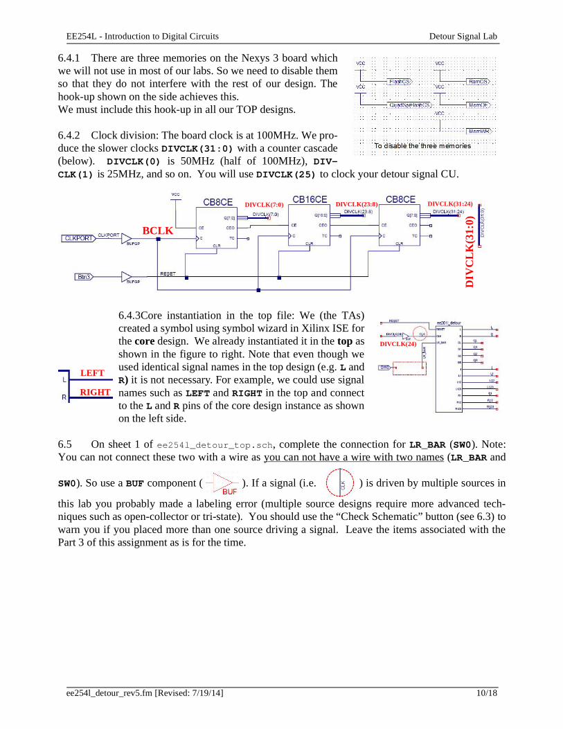
6.4.1 There are three memories on the Nexys 3 board whichwe will not use in most of our labs. So we need to disable themso that they do not interfere with the rest of our design. Thehook-up shown on the side achieves this.We must include this hook-up in all our TOP designs.
6.4.2 Clock division: The board clock is at 100MHz. We pro-duce the slower clocks DIVCLK(31:0) with a counter cascade(below). DIVCLK(0) is 50MHz (half of 100MHz), DIV-CLK(1) is 25MHz, and so on. You will use DIVCLK(25) to clock your detour signal CU.
6.4.3Core instantiation in the top file: We (the TAs)created a symbol using symbol wizard in Xilinx ISE forthe core design. We already instantiated it in the top asshown in the figure to right. Note that even though weused identical signal names in the top design (e.g. L andR) it is not necessary. For example, we could use signalnames such as LEFT and RIGHT in the top and connectto the L and R pins of the core design instance as shownon the left side.
6.5 On sheet 1 of ee254l_detour_top.sch, complete the connection for LR_BAR (SW0). Note:You can not connect these two with a wire as you can not have a wire with two names (LR_BAR and
SW0). So use a BUF component ( ). If a signal (i.e. ) is driven by multiple sources in
this lab you probably made a labeling error (multiple source designs require more advanced tech-niques such as open-collector or tri-state). You should use the “Check Schematic” button (see 6.3) towarn you if you placed more than one source driving a signal. Leave the items associated with thePart 3 of this assignment as is for the time.
BCLK
DIV
CLK
(31:
0)
DIVCLK(7:0) DIVCLK(23:8) DIVCLK(31:24)
LEFT
RIGHT
DIVCLK(24)
EE254L - Introduction to Digital Circuits Detour Signal Lab
ee254l_detour_rev5.fm [Revised: 7/19/14] 11/18
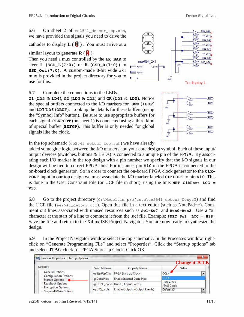
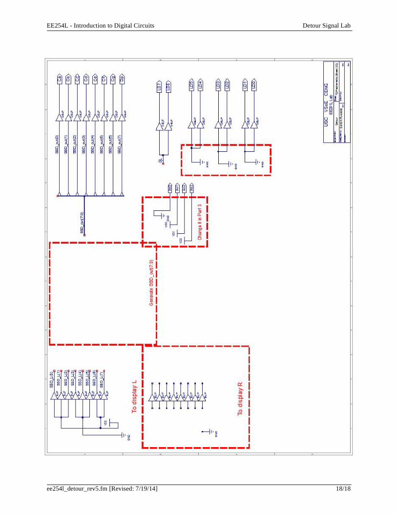
6.6 On sheet 2 of ee254l_detour_top.sch,we have provided the signals you need to drive the
cathodes to display L ( ) . You must arrive at a
similar layout to generate R ( ). Then you need a mux controlled by the LR_BAR tosteer L (SSD_L(7:0)) or R (SSD_R(7:0)) toSSD_Out(7:0). A custom-made 8-bit wide 2x1mux is provided in the project directory for you touse for this.
6.7 Complete the connections to the LEDs.G1 (LD5 & LD4), G2 (LD3 & LD2) and GR (LD1 & LD0). Noticethe special buffers connected to the I/O markers for SW0 (IBUF)and LD7/LD6 (OBUF). Look up the details for these buffers (usingthe “Symbol Info” button). Be sure to use appropriate buffers foreach signal. CLKPORT (on sheet 1) is connected using a third kindof special buffer (BUFGP). This buffer is only needed for globalsignals like the clock.
In the top schematic (ee254l_detour_top.sch) we have alreadyadded some glue logic between the I/O markers and your core design symbol. Each of these input/output devices (switches, buttons & LEDs) is connected to a unique pin of the FPGA. By associ-ating each I/O marker in the top design with a pin number we specify that the I/O signals in ourdesign will be tied to correct FPGA pins. For instance, pin V10 of the FPGA is connected to theon-board clock generator. So in order to connect the on-board FPGA clock generator to the CLK-PORT input in our top design we must associate the I/O marker labeled CLKPORT to pin V10. Thisis done in the User Constraint File (or UCF file in short), using the line: NET ClkPort LOC =V10;
6.8 Go to the project directory (C:\Modelsim_projects\ee254l_detour_Nexys3) and findthe UCF file (ee254l_detour.ucf). Open this file in a text editor (such as NotePad++). Com-ment out lines associated with unused resources such as Sw1-Sw7 and Btn0-Btn2. Use a “#”character at the start of a line to comment it from the .ucf file. Example: #NET Sw1 LOC = H18;Save the file and return to the Xilinx ISE Project Navigator. You are now ready to synthesize thedesign.
6.9 In the Project Navigator window select the top schematic. In the Processes window, right-click on “Generate Programming File” and select “Properties”. Click the “Startup options” taband select JTAG clock for FPGA Start-Up Clock. Click OK.
Change it JCLK
EE254L - Introduction to Digital Circuits Detour Signal Lab
ee254l_detour_rev5.fm [Revised: 7/19/14] 12/18
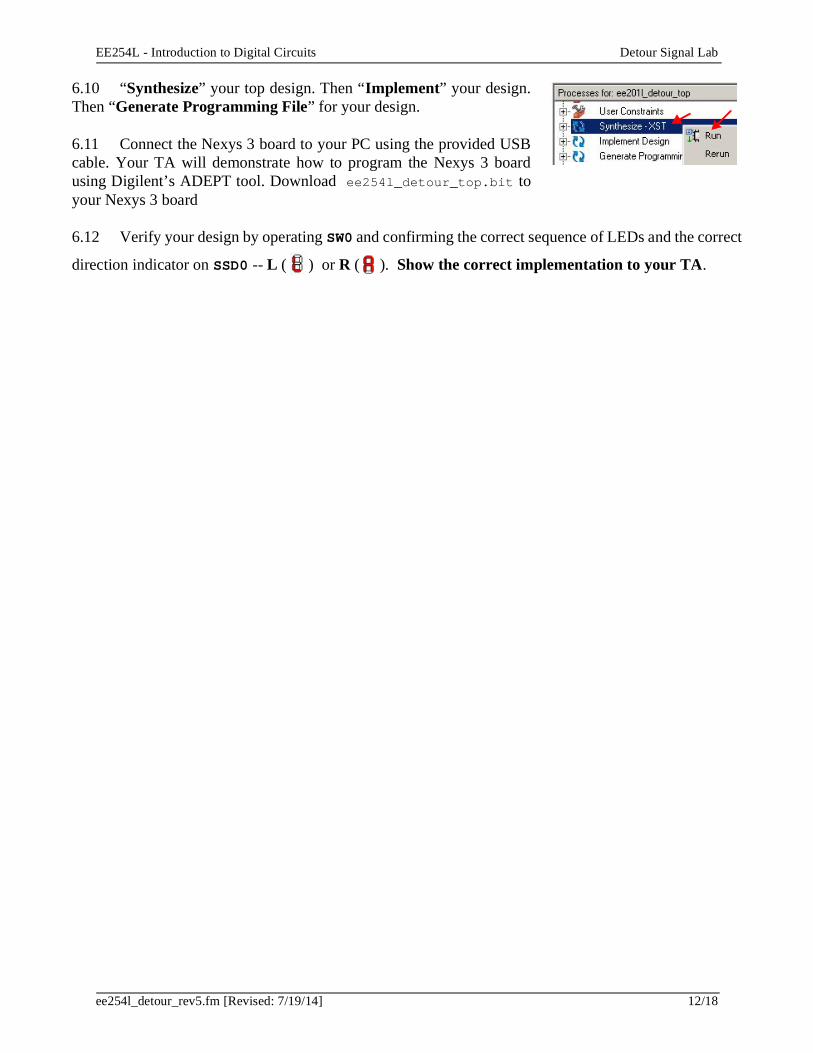
6.10 “Synthesize” your top design. Then “Implement” your design.Then “Generate Programming File” for your design.
6.11 Connect the Nexys 3 board to your PC using the provided USBcable. Your TA will demonstrate how to program the Nexys 3 boardusing Digilent’s ADEPT tool. Download ee254l_detour_top.bit toyour Nexys 3 board
6.12 Verify your design by operating SW0 and confirming the correct sequence of LEDs and the correct
direction indicator on SSD0 -- L ( ) or R ( ). Show the correct implementation to your TA.
EE254L - Introduction to Digital Circuits Detour Signal Lab
ee254l_detour_rev5.fm [Revised: 7/19/14] 13/18
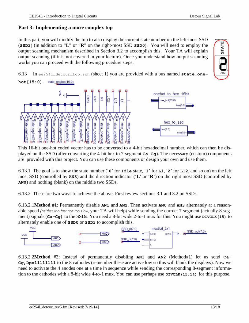
Part 3: Implementing a more complex top
In this part, you will modify the top to also display the current state number on the left-most SSD(SSD3) (in addition to “L” or “R” on the right-most SSD SSD0). You will need to employ theoutput scanning mechanism described in Section 3.2 to accomplish this. Your TA will explainoutput scanning (if it is not covered in your lecture). Once you understand how output scanningworks you can proceed with the following procedure steps.
6.13 In ee254l_detour_top.sch (sheet 1) you are provided with a bus named state_one-hot[15:0].
This 16-bit one-hot coded vector has to be converted to a 4-bit hexadecimal number, which can then be dis-played on the SSD (after converting the 4-bit hex to 7-segment Ca-Cg). The necessary (custom) componentsare provided with this project. You can use these components or design your own and use them.
6.13.1 The goal is to show the state number (‘0’ for Idle state, ‘1’ for L1, ‘2’ for L12, and so on) on the leftmost SSD (controlled by AN3) and the direction indicator (‘L’ or ‘R’) on the right most SSD (controlled byAN0) and nothing (blank) on the middle two SSDs.
6.13.2 There are two ways to achieve the above. First review sections 3.1 and 3.2 on SSDs.
6.13.2.1Method #1: Permanently disable AN1 and AN2. Then activate AN0 and AN3 alternately at a reason-able speed (neither too fast nor too slow, your TA will help) while sending the correct 7-segment (actually 8-seg-ment) signals (Ca-Cg) to the SSDs. You need a 8-bit wide 2-to-1 mux for this. You might use DIVCLK(15) toalternately enable one of SSD0 or SSD3 to accomplish this.
6.13.2.2Method #2: Instead of permanently disabling AN1 and AN2 (Method#1) let us send Ca-Cg,Dp=11111111 to the 8 cathodes (remember these are active low so this will blank the displays). Now weneed to activate the 4 anodes one at a time in sequence while sending the corresponding 8-segment informa-tion to the cathodes with a 8-bit wide 4-to-1 mux. You can use perhaps use DIVCLK(15:14) for this purpose.
EE254L - Introduction to Digital Circuits Detour Signal Lab
ee254l_detour_rev5.fm [Revised: 7/19/14] 14/18
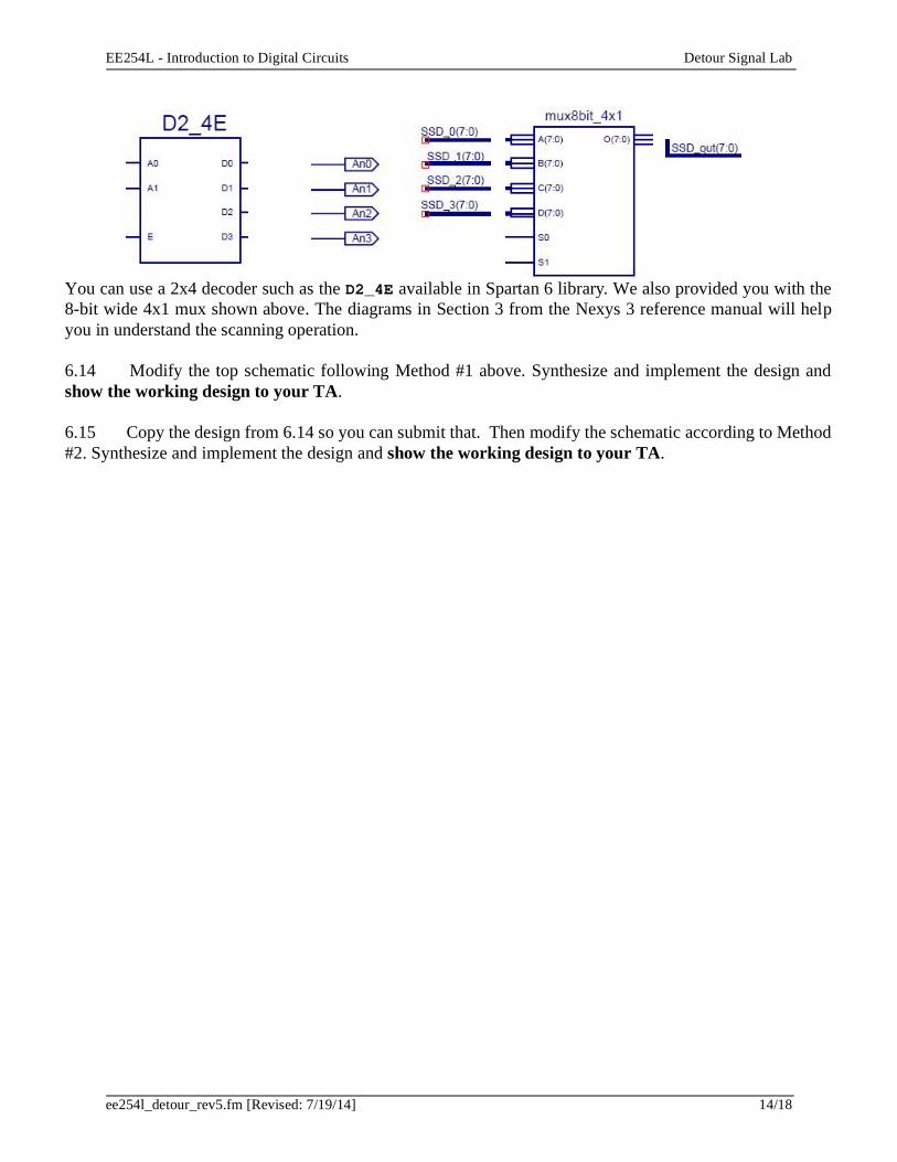
You can use a 2x4 decoder such as the D2_4E available in Spartan 6 library. We also provided you with the8-bit wide 4x1 mux shown above. The diagrams in Section 3 from the Nexys 3 reference manual will helpyou in understand the scanning operation.
6.14 Modify the top schematic following Method #1 above. Synthesize and implement the design andshow the working design to your TA.
6.15 Copy the design from 6.14 so you can submit that. Then modify the schematic according to Method#2. Synthesize and implement the design and show the working design to your TA.
EE254L - Introduction to Digital Circuits Detour Signal Lab
ee254l_detour_rev5.fm [Revised: 7/19/14] 15/18
7. Lab Report:
Q 7. 1: What are the two different D-flip-flops that we are using in this lab? What is the difference between them? (2pts)
Q 7. 2: Name 2 more D-flip-flops that are available in the Xilinx library and briefly explain how are they different from the ones that we are using in this lab.(8pts)
Q 7. 3: Which pin of the FPGA is connected to the BtnC on the Nexys 3 board?. (4pts)
Q 7. 4: Which three special buffers are needed for signals that connect to the input and output devices (including the on-board clock generator) ? Give their names and whether they are needed to con-nect inputs or outputs or both. (6pts)
Q 7. 5: The frequency of the clock entering the FPGA is 100MHz. Notice that we are dividing the input clock by using counters. Calculate the frequency of the divided clock that triggers the detour sig-nal state machine. (5pts)
Q 7. 6: Why are we dividing the clock? (5pts)
Q 7. 7: Do we need to maintain any relation between the output scanning frequency and the divided sys-tem clock used in the core state machine? Does one need to be faster than the other? Can one be a multiple of the other (say 4 times, 27 times)? Note that in real-life designs, the system clock frequency is much higher than
the rate at which the detour arrow grows or traffic lights change. Timers are used to control timing of such events. (5 pts)
Name:_________________________ Date: _________________________Lab Session: ___________________ TA’s Signature: __________________
For TAs: Pre-lab (15): _____ Implementation (50): _____ Report (out of 35): ___
Comments:
EE254L - Introduction to Digital Circuits Detour Signal Lab
ee254l_detour_rev5.fm [Revised: 7/19/14] 16/18
EE254L - Introduction to Digital Circuits Detour Signal Lab
ee254l_detour_rev5.fm [Revised: 7/19/14] 17/18
EE254L - Introduction to Digital Circuits Detour Signal Lab
ee254l_detour_rev5.fm [Revised: 7/19/14] 18/18