Embed Size (px)
Citation preview

Computer Architecture and Organization:
L03: Register transfer and System Bus
By: A. H. Abdul Hafez [email protected], [email protected]
October 12, 2016 1 CAO, by Dr. A.H. Abdul Hafez, CE Dept. HKU

Outlines
October 12, 2016 CAO, by Dr. A.H. Abdul Hafez, CE Dept. HKU 2
1. Registers 2. Micro-operation 3. Register transfer 4. Simultaneous Register Transfers 5. Illegal Simultaneous Register Transfers 6. Bus transfer 7. Bus system 8. Constructing bus system using multiplexers 9. Constructing bus system using three-state buffers 10. Memory transfer 11. Arithmetic microoperation 12. Full adder 13. Four bit parallel adder 14. End

Registers
October 12, 2016 CAO, by Dr. A.H. Abdul Hafez, CE Dept. HKU 3
A register is a group of flip flops, each of which is capable of storing one bit of information.
Clock inputs triggers all flip flops at the positive (rising) edge of each pulse.
Clear input (low active) reset the all outputs to 0s. It must be 1 in normal operation. Four bits
register

Register with parallel load
October 12, 2016 CAO, by Dr. A.H. Abdul Hafez, CE Dept. HKU 4
Transferring new information into the register is called loading the register.
If all the bits of register are loaded simultaneously with a common clock pulse, the loading is called parallel load.
To leave the content of the register unchanged, the input must held constant or the clock should be prohibited.
The additional circuits play the role of MUX whose outputs drive data to the register either from the data bus or from the output of the register it self.

Shift register
October 12, 2016 CAO, by Dr. A.H. Abdul Hafez, CE Dept. HKU 5
A register that is capable of shifting the binary data from its current cell to a neighbor cell.
The logical configuration is a chain of flip flops. The output of one flip flop is connected to the input of the next flip flop. All flip flops are connected to a common clock.

Single Flip-Flop can save information of 1 bit. To save n-bit, we need n Flip Flops connected together. We have then n bits
register. Shift Register is a group of Flip Flops connected together to save and shift n-bit
data. Different types of Shift Registers are available:
12-Oct-16 6 Computer Organizatrion - Dr. Abdul Hafez, ATRI
Registers

Microoperations
The operations that are performed on the data stored in registers are called microoperations. Examples of microoperations are: transfer, shift, clear and load.
Digital modulus ( Ex: microprocessor) are best defined by the
registers they contain and the operations that performed on the data stored in them. Microoperations are the basis for Microprocessors. An instruction
is fetched from memory, decoded and executed by performing a sequence of microoperations. A microprocessor performs the microoperations in order to realize
the instruction. 12-Oct-16 7 Computer Organizatrion - Dr. Abdul Hafez, ATRI

Hardware organization
• Internal hardware organization of a computer is best defined by:
1. The set of registers.
2. The sequence of Microoperations performed on these registers.
3. The control that initiates the sequence of Microoperations.
12-Oct-16 8 Computer Organizatrion - Dr. Abdul Hafez, ATRI

Register Representation
R1
R2
7 6 5 4 3 2 1 0
PC (H) PC (L)
(a) Register R
(c) Numbering of bits
15 0 15 8 7 0
(d) Divided into two parts
(b) Showing individual bits
Computer registers are designated by capital letters (sometimes followed by numerals) to define the function of the register. Examples: R1 processor register, PC Program Counter, AC Accumulator.
In diagrams, the registers are represented by rectangular box with the name of the register inside as shown in the Figure.
The individual flip-flops (bits) are distinguished by writing the location number of the bit as in (b) or ( c) and (d) in the figure.
12-Oct-16 9 Computer Organizatrion - Dr. Abdul Hafez, ATRI

Symbol Description Examples
Letters (and numerals)
Denotes a register MAR, R2
Parentheses ( ) Denotes a part of a Register
R2(0-7), R2(L)
Arrow ← Denotes transfer of information
R2←R1
Comma , Separates two microopeartions
R2←R1, R1←R2
Basic Symbols for Register Transfers
12-Oct-16 10 Computer Organizatrion - Dr. Abdul Hafez, ATRI

Register Transfer R2 ← R1 denotes a transfer of the content (copy) of register R1 (source register) into register R2 (destination register). P: R2 ← R1 When condition P occurs, the contents of register R1 are copied into register R2. Alternatively, we can say if (P=1) then ( R2 ← R1 ). P is a control signal generated in the control circuit. Every statement written in a register transfer notation implies a hardware construction for implementing the transfer. The circuit diagram for the register transfer P: R2 ← R1 is shown below.
R2
R1
Control circuit
n
Clock P- Load
(a) block diagram
Transfer occurs here
(b) Timing diagram 12-Oct-16 11 Computer Organizatrion - Dr. Abdul Hafez, ATRI

Simultaneous Register Transfers
T: R2 ← R1, R3 ← R1 When signal T is asserted, the contents of R1 are copied into both registers R2 and R3. Note that the order in which the statement is written does not matter. T: R2 ← R1, R4 ← R3 two registers (R2 and R4) are loaded simultaneously from different sources.
R2
R1
R3
T T
T: R2 ← R1, R3 ← R1
R2
R4
R1
R3
T
T: R2 ← R1, R4 ← R3
12-Oct-16 12 Computer Organizatrion - Dr. Abdul Hafez, ATRI

Illegal Simultaneous Transfers
Example of an illegal operation is shown below, since A is loaded with two different values simultaneously.
Solution
12-Oct-16 13 Computer Organizatrion - Dr. Abdul Hafez, ATRI
A
B
C
MUX
0
1
P: A ← B Q: A ← C
Q P V Q
Register A can receive data from more than one source, depending on the control signal asserted. A multiplexer is used to determine the data to be loaded, although tri-state buffers could also have been used.

Bus Transfers A typical digital computer has many registers, and paths (lines) must be provided to
transfer information (data) from one register to another. For n registers system, the number of wires will be excessive if separate lines are used
between each register and all other registers in the system !
R1 R2
R3
R4 R5
R6
To connect n items with direct connections, you need n(n-1)/2 connections. October 12, 2016 14 CAO, by Dr. A.H. Abdul Hafez, CE Dept. HKU

Bus System A more efficient scheme for transferring information between registers in a
multiple-register configuration is a common bus system. A bus system consists of a set of common lines, one for each bit of a register,
through which binary information is transferred one at a time. Control signals determine which register is selected by the bus during each
particular transfer.
To connect n items with bus connections, you need only n connections.
R1 R2
R3
R4 R5
R6 Common Bus
October 12, 2016 15 CAO, by Dr. A.H. Abdul Hafez, CE Dept. HKU

Constructing bus system using multiplexers The multiplexer selects one of the four registers as the source register. Control
lines for the MUX are driven by external circuitry. The data is made available to all registers, but only one actually loads the data. Again, external hardware generates load signals for the four registers such that no more than one is active at any given time.
P: A B Q: A C R: B D S: C A T: D C U: D B
The symbolic statement for a bus transfer may mention the bus or its presence may be implied in the statement. When bus is included in the statement we write:
BUS C, A BUS (however it is A C)
October 12, 2016 16 CAO, by Dr. A.H. Abdul Hafez, CE Dept. HKU

Detail connection of the Bus system for 4 registers
4X1 MUX 0
4X1 MUX 1
4X1 MUX 2
4X1 MUX 3
3 2 1 0 3 2 1 0 3 2 1 0 3 2 1 0
3 2 1 0 3 2 1 0 3 2 1 0 3 2 1 0
A2 A1 A0 B2 B1 B0 C2 C1 C0 D2 D1 D0
D0 C0 B0 A0 D1 C1 B1 A1 D2 C2 B2 A2
4-line Common bus
Register A Register B Register C Register D
S0 S1 0 0
A0 A1
A2
A3
October 12, 2016 17 CAO, by Dr. A.H. Abdul Hafez, CE Dept. HKU

In general, a bus system will multiplex k registres of n bit each to produce an n-line common bus. 1- The number of multiplexers needed to construct the bus is equal to n, the number of bits in each register. 2- The size of each multiplexer must be k x 1 since it multiplexes k data lines.
# example: a common bus of 8 registers of 16 bits each requires 16 multiplexers, one for each line in the bus. Each MUX must have 8 input lines and three selector lines to multiplex one bit in the 8 registers.
October 12, 2016 18 CAO, by Dr. A.H. Abdul Hafez, CE Dept. HKU
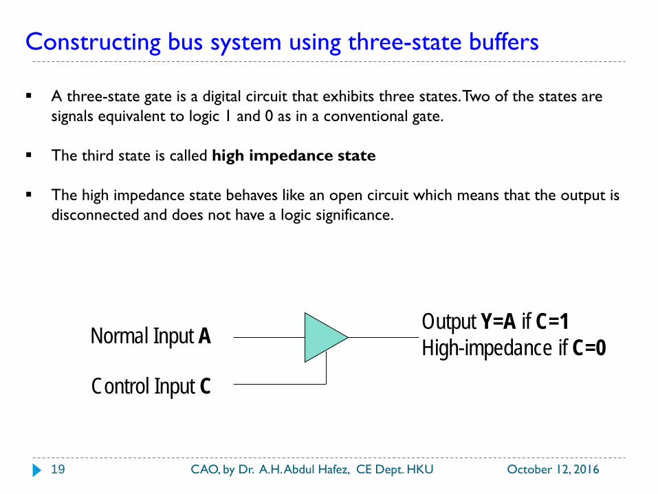
Constructing bus system using three-state buffers
A three-state gate is a digital circuit that exhibits three states. Two of the states are signals equivalent to logic 1 and 0 as in a conventional gate.
The third state is called high impedance state
The high impedance state behaves like an open circuit which means that the output is disconnected and does not have a logic significance.
Normal Input A
Control Input C
Output Y=A if C=1 High-impedance if C=0
October 12, 2016 19 CAO, by Dr. A.H. Abdul Hafez, CE Dept. HKU

A0 B0 C0 D0
2 X 4 Decoder
0 1 2 3
S0
S1
Register A
3 2 1 0
A1 B1 C1 D1
2 X 4 Decoder
0 1 2 3
S0
S1
Register B
3 2 1 0
A2 B2 C2 D2
2 X 4 Decoder
0 1 2 3
S0
S1
Register C
3 2 1 0
A3 B3 C3 D3
2 X 4 Decoder
0 1 2 3
S0
S1
Register D
3 2 1 0
S0
S1
A0 A1 A2 A3 B0 B1 B2 B3 C2 C1 C3 C0 D0 D1 D2 D3
Bit 0
Bit 1
Bit 2
Bit 3 Bus lines
4-line Bus system using three state-buffer
October 12, 2016 20 CAO, by Dr. A.H. Abdul Hafez, CE Dept. HKU

Memory Transfer
Memory Unit
DR
Microprocessor
Address lines
Data lines
Write
Read
Read operation
Write operation
Read: DR← M[AR]
Write: M[AR] ← DR
October 12, 2016 21 CAO, by Dr. A.H. Abdul Hafez, CE Dept. HKU

Main Types of Microoperations in Digital Computers
October 12, 2016 CAO, by Dr. A.H. Abdul Hafez, CE Dept. HKU 22
1. Register Transfer Microoperations transfer binary information from one register to another.
2. Arithmetic Microoperations perform arithmetic operations on numeric data stored in registers.
3. Logic Microoperations perform bit manipulation operations on (non-numeric) data stored in registers.
4. Shift Microoperations perform shift operations on data stored in registers.

Arithmetic Microoperations
October 12, 2016 CAO, by Dr. A.H. Abdul Hafez, CE Dept. HKU 23
Symbolic Designation Description
R3 R1 + R2 Contents of R1 plus R2 transferred to R3 R3 R1 – R2 Contents of R1 minus R2 transferred to R3 R2 R’2 Complement of the contents of R2 (1’s complement) R2 R’2 + 1 2’s complement of the contents of R2 R3 R1 + R’2 + 1 R1 plus the 2’s complement of R2 (subtraction) R1 R1 + 1 Increment the contents of R1 by one R1 R1 -1 Decrement the contents of R1 by one

The full Adder Half Adder
0 0 0 0 0 0 0 1 0 1 0 1 0 0 1 0 1 1 1 0 1 0 0 0 1 1 0 1 1 0 1 1 0 1 0 1 1 1 1 1
c = xy s = xy’ + x’y = x ⊕ y
x y c
s
x y
cn-1
S
cn
Full Adder
0 0 0 0 0 1 0 1 1 0 0 1 1 1 1 0
x y c s
x y cn-1 cn s
October 12, 2016 24 CAO, by Dr. A.H. Abdul Hafez, CE Dept. HKU
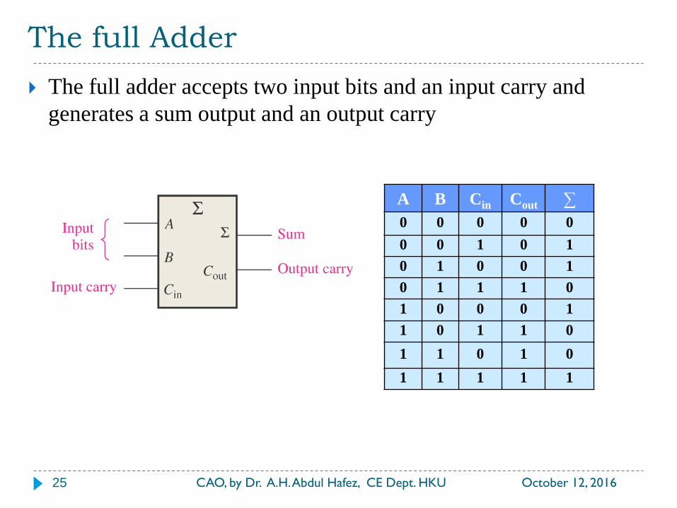
The full Adder
October 12, 2016 CAO, by Dr. A.H. Abdul Hafez, CE Dept. HKU 25
The full adder accepts two input bits and an input carry and generates a sum output and an output carry
A B Cin Cout ∑ 0 0 0 0 0 0 0 1 0 1 0 1 0 0 1 0 1 1 1 0 1 0 0 0 1 1 0 1 1 0 1 1 0 1 0 1 1 1 1 1

Four-bits parallel adder
October 12, 2016 CAO, by Dr. A.H. Abdul Hafez, CE Dept. HKU 26

The end of the Lecture
October 12, 2016 CAO, by Dr. A.H. Abdul Hafez, CE Dept. HKU 27
Thanks for your time Questions are welcome


![Estruc. Organiz. y Dotacion de Personal Neferm. Oct 06[1]](https://img.pdfslide.us/doc/110x75/5571fe4249795991699afd6f/estruc-organiz-y-dotacion-de-personal-neferm-oct-061.jpg)