Embed Size (px)
Citation preview

Data Sheet
1A LOW NOISE CMOS LDO REGULATOR WITH ENABLE AP2114
Jan. 2013 Rev. 2. 2 BCD Semiconductor Manufacturing Limited
1
General Description The AP2114 is CMOS process low dropout linear regulator with enable function, the regulator delivers a guaranteed 1A (Min) continuous load current. The AP2114 features low power consumption. The AP2114 is available in 1.2V, 1.5V, 1.8V, 2.5V and 3.3V regulator output and 0.8V to 5V adjustable output, and available in excellent output accuracy ±1.5%, it is also available in an excellent load regulation and line regulation performance.
The AP2114 is available in standard packages of SOT-223, TO-252-2 (1), TO-252-2 (3), TO-252-2 (4), TO-263-3, SOIC-8 and PSOP-8.
Features • Output Voltage Accuracy: ±1.5% • Output Current: 1A (Min) • Fold-back Short Current Protection: 50mA • Low Dropout Voltage (3.3V): 450mV (Typ)
@IOUT=1A • Stable with 4.7μF Flexible Cap: Ceramic,
Tantalum and Aluminum Electrolytic • Excellent Line Regulation: 0.02%/V (Typ),
0.1%/V (Max) @ IOUT=30mA • Excellent Load Regulation: 0.2%A (Typ) @
IOUT=1mA to 1A • Low Quiescent Current: 60μA (1.2V/1.5V/1.8V /2.5V/ADJ) • Low Output Noise: 30μVRMS • PSRR: 68dB @ Freq=1KHz (1.2V/1.5V/1.8V /ADJ) • OTSD Protection • Operating Temperature Range: -40°C to 85°C • ESD: MM 400V, HBM 4000V Applications • LCD Monitor • LCD TV • STB
Figure 1. Package Types of AP2114
SOT-223 TO-263-3 TO-252-2 (1)
TO-252-2 (3) TO-252-2 (4) SOIC-8 PSOP-8

Data Sheet
1A LOW NOISE CMOS LDO REGULATOR WITH ENABLE AP2114
Jan. 2013 Rev. 2. 2 BCD Semiconductor Manufacturing Limited
2
Pin Configuration
H/HA Package S Package (SOT-223) (TO-263-3)
H HA
D/DA Package
D DA
(TO-252-2 (1)) (TO-252-2 (3)) (TO-252-2 (1)) (TO-252-2 (3))
(TO-252-2 (4)) (TO-252-2 (4))
M Package MP Package (SOIC-8) (PSOP-8)
For Fixed Versions For Adjustable Version For Fixed Versions For Adjustable Version
Figure 2. Pin Configuration of AP2114 (Top View)
1
2
3
GND
VIN
VOUTVOUT
1
2
3
GND
VIN
VOUT
GND
1
2
3
4
8
7
6
5
GND
VOUT
GND
VIN
EN
GND
GND
GND
1
2
3
4
8
7
6
5
GND
VOUT
GND
VIN
EN
GND
GND
GND
1
2
3
4
8
7
6
5
VIN
EN
VOUT
GND
ADJ
GNDGND
GND
VIN
EN
VOUT
GND
ADJ
GNDGND
GND
1
2
3
4
8
7
6
5
1
2
3 VIN
VOUT
GND
VOUT
1
2
3
VIN
VOUT
GNDGND
1
2
3
VIN
VOUT
GNDGND
1
2
3 VIN
VOUT
GND
VOUT

Data Sheet
1A LOW NOISE CMOS LDO REGULATOR WITH ENABLE AP2114
Jan. 2013 Rev. 2. 2 BCD Semiconductor Manufacturing Limited
3
Pin Descriptions
Pin Number
Pin Name
Function SOT-223 (H),
TO-263-3, TO-252-2 (1) (D) TO-252-2 (3) (D) TO-252-2 (4) (D)
SOT-223 (HA), TO-252-2 (1) (DA) TO-252-2 (3) (DA) TO-252-2 (4) (DA)
SOIC-8, PSOP-8 (Fixed)
SOIC-8, PSOP-8 (ADJ)
1 2 1, 3, 5, 6, 7 2, 3, 5, 7 GND Ground 2 3 2 8 VOUT Regulated Output 3 1 4 1 VIN Input Voltage Pin
8 4 EN Chip Enable, H–Normal Work, L– Shutdown Output
6 ADJ Adjust Output
Functional Block Diagram
For Fixed Versions
Shutdown Logic
Thermal Shutdown
Foldback Current Limit
VREF
GND
EN VIN
3MΩVOUT
A (B)A: SOT-223 , TO-263-3 , TO-252- 2 (1)/(3B: SOIC-8 , PSOP-8
(8)
1 (1 , 3 , 5 , 6 , 7)
2 (2)
3 (4)
{2}
{3}
{1}
{C}(H)
C: SOT-223 , (HA) TO-252- 2 (1)/(3 (DA)
4)(D))/(
)/(4)

Data Sheet
1A LOW NOISE CMOS LDO REGULATOR WITH ENABLE AP2114
Jan. 2013 Rev. 2. 2 BCD Semiconductor Manufacturing Limited
4
Functional Block Diagram (Continued)
For ADJ Version
Figure 3. Functional Block Diagram of AP2114
Shutdown Logic
Thermal Shutdown
Foldback Current Limit
VREF
GND
EN VIN
3 Ω
VOUT
SOIC-8 , PSOP-8
8
1
ADJ
4
6
M
2, 3, 5, 7
Data Sheet
1A LOW NOISE CMOS LDO REGULATOR WITH ENABLE AP2114
Jan. 2013 Rev. 2. 2 BCD Semiconductor Manufacturing Limited
5
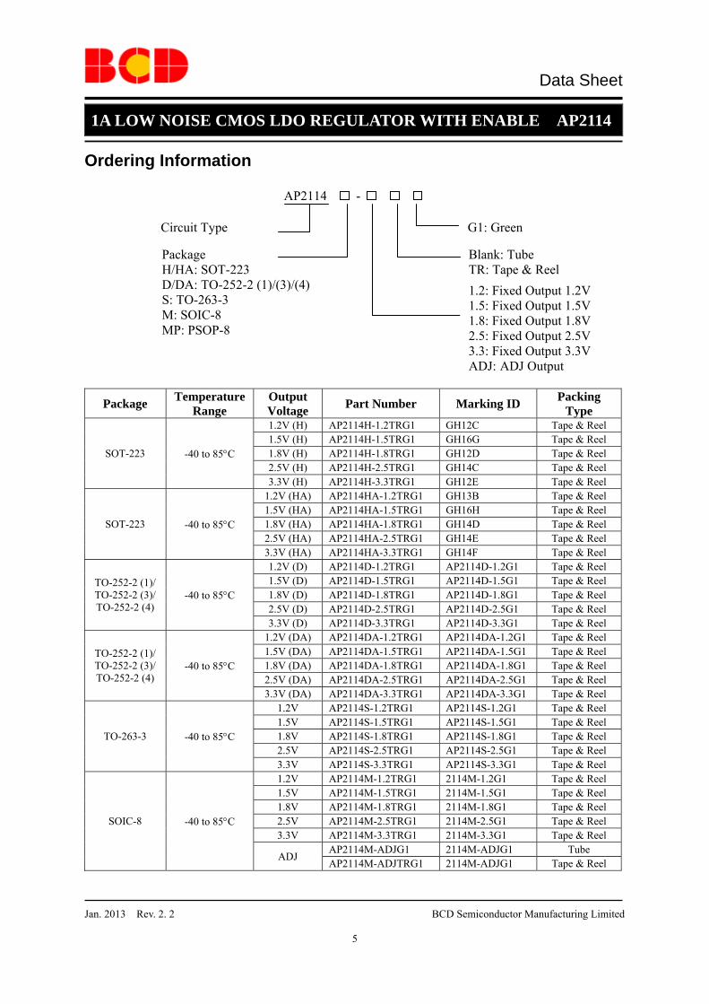
Ordering Information
AP2114 -
Circuit Type G1: Green
Package Temperature Range
Output Voltage Part Number Marking ID Packing
Type
SOT-223 -40 to 85°C
1.2V (H) AP2114H-1.2TRG1 GH12C Tape & Reel 1.5V (H) AP2114H-1.5TRG1 GH16G Tape & Reel 1.8V (H) AP2114H-1.8TRG1 GH12D Tape & Reel 2.5V (H) AP2114H-2.5TRG1 GH14C Tape & Reel 3.3V (H) AP2114H-3.3TRG1 GH12E Tape & Reel
SOT-223 -40 to 85°C
1.2V (HA) AP2114HA-1.2TRG1 GH13B Tape & Reel 1.5V (HA) AP2114HA-1.5TRG1 GH16H Tape & Reel 1.8V (HA) AP2114HA-1.8TRG1 GH14D Tape & Reel 2.5V (HA) AP2114HA-2.5TRG1 GH14E Tape & Reel 3.3V (HA) AP2114HA-3.3TRG1 GH14F Tape & Reel
TO-252-2 (1)/ TO-252-2 (3)/ TO-252-2 (4)
-40 to 85°C
1.2V (D) AP2114D-1.2TRG1 AP2114D-1.2G1 Tape & Reel 1.5V (D) AP2114D-1.5TRG1 AP2114D-1.5G1 Tape & Reel 1.8V (D) AP2114D-1.8TRG1 AP2114D-1.8G1 Tape & Reel 2.5V (D) AP2114D-2.5TRG1 AP2114D-2.5G1 Tape & Reel 3.3V (D) AP2114D-3.3TRG1 AP2114D-3.3G1 Tape & Reel
TO-252-2 (1)/ TO-252-2 (3)/ TO-252-2 (4)
-40 to 85°C
1.2V (DA) AP2114DA-1.2TRG1 AP2114DA-1.2G1 Tape & Reel 1.5V (DA) AP2114DA-1.5TRG1 AP2114DA-1.5G1 Tape & Reel 1.8V (DA) AP2114DA-1.8TRG1 AP2114DA-1.8G1 Tape & Reel 2.5V (DA) AP2114DA-2.5TRG1 AP2114DA-2.5G1 Tape & Reel 3.3V (DA) AP2114DA-3.3TRG1 AP2114DA-3.3G1 Tape & Reel
TO-263-3 -40 to 85°C
1.2V AP2114S-1.2TRG1 AP2114S-1.2G1 Tape & Reel 1.5V AP2114S-1.5TRG1 AP2114S-1.5G1 Tape & Reel 1.8V AP2114S-1.8TRG1 AP2114S-1.8G1 Tape & Reel 2.5V AP2114S-2.5TRG1 AP2114S-2.5G1 Tape & Reel 3.3V AP2114S-3.3TRG1 AP2114S-3.3G1 Tape & Reel
SOIC-8 -40 to 85°C
1.2V AP2114M-1.2TRG1 2114M-1.2G1 Tape & Reel 1.5V AP2114M-1.5TRG1 2114M-1.5G1 Tape & Reel 1.8V AP2114M-1.8TRG1 2114M-1.8G1 Tape & Reel 2.5V AP2114M-2.5TRG1 2114M-2.5G1 Tape & Reel 3.3V AP2114M-3.3TRG1 2114M-3.3G1 Tape & Reel
ADJ AP2114M-ADJG1 2114M-ADJG1 Tube AP2114M-ADJTRG1 2114M-ADJG1 Tape & Reel
Blank: Tube TR: Tape & Reel 1.2: Fixed Output 1.2V1.5: Fixed Output 1.5V1.8: Fixed Output 1.8V2.5: Fixed Output 2.5V3.3: Fixed Output 3.3VADJ: ADJ Output
Package H/HA: SOT-223 D/DA: TO-252-2 (1)/(3)/(4)S: TO-263-3 M: SOIC-8 MP: PSOP-8

Data Sheet
1A LOW NOISE CMOS LDO REGULATOR WITH ENABLE AP2114
Jan. 2013 Rev. 2. 2 BCD Semiconductor Manufacturing Limited
6
Ordering Information (Continued)
Package Temperature Range
Output Voltage Part Number Marking ID Packing
Type
PSOP-8 -40 to 85°C
1.2V AP2114MP-1.2TRG1 2114MP-1.2G1 Tape & Reel 1.5V AP2114MP-1.5TRG1 2114MP-1.5G1 Tape & Reel 1.8V AP2114MP-1.8TRG1 2114MP-1.8G1 Tape & Reel 2.5V AP2114MP-2.5TRG1 2114MP-2.5G1 Tape & Reel 3.3V AP2114MP-3.3TRG1 2114MP-3.3G1 Tape & Reel
ADJ AP2114MP-ADJG1 2114MP-ADJG1 Tube AP2114MP-ADJTRG1 2114MP-ADJG1 Tape & Reel
BCD Semiconductor's Pb-free products, as designated with "G1" suffix in the part number, are RoHS compliant and Green.

Data Sheet
1A LOW NOISE CMOS LDO REGULATOR WITH ENABLE AP2114
Jan. 2013 Rev. 2. 2 BCD Semiconductor Manufacturing Limited
7
Absolute Maximum Ratings (Note 1) Parameter Symbol Value Unit Power Supply Voltage VIN 6.5 V Operating Junction Temperature Range TJ 150 ºC
Storage Temperature Range TSTG -65 to 150 ºC
Lead Temperature (Soldering, 10sec) TLEAD 260 ºC
Thermal Resistance (Junction to Ambient)(No Heatsink) θJA
SOIC-8 144
°C/W
PSOP-8 143
SOT-223 128 TO-252-2 (1)/ TO-252-2 (3)/ TO-252-2 (4)
90
TO-263-3 73
ESD (Machine Model) 400 V
ESD (Human Body Model) 4000 V
Note 1: Stresses greater than those listed under “Absolute Maximum Ratings” may cause permanent damage to the device. These are stress ratings only, and functional operation of the device at these or any other conditions beyond those indicated under “Recommended Operating Conditions” is not implied. Exposure to “Absolute Maximum Ratings” for extended periods may affect device reliability. Recommended Operating Conditions Parameter Symbol Min Max Unit Supply Voltage VIN 2.5 6.0 V Operating Ambient Temperature Range TA -40 85 °C

Data Sheet
1A LOW NOISE CMOS LDO REGULATOR WITH ENABLE AP2114
Jan. 2013 Rev. 2. 2 BCD Semiconductor Manufacturing Limited
8
Electrical Characteristics
AP2114-1.2 Electrical Characteristics (Note 2) (VIN=2.5V, CIN=4.7μF (Ceramic), COUT=4.7μF (Ceramic), Typical TA= 25°C, Bold typeface applies over -40OC≤TA≤85OC ranges, unless otherwise specified (Note 3))
Parameter Symbol Test Conditions Min Typ Max Unit
Output Voltage VOUT VIN =2.5V, 1mA ≤ IOUT ≤ 30mA VOUT ×98.5% 1.2 VOUT
×101.5% V
Input Voltage VIN 6.0 V
Maximum Output Current IOUT(MAX) VIN=2.5V, VOUT=1.182V to 1.218V 1 A
Load Regulation △VOUT/VOUT
I△ OUT VIN=2.5V, 1mA ≤ IOUT ≤1A 0.2 1 %/A
Line Regulation △VOUT/VOUT V△ IN
2.5V≤VIN≤6V, IOUT=30mA -0.1 0.02 0.1 %/V
Dropout Voltage VDROP IOUT=1.0A 1200 1300 mV
Quiescent Current IQ VIN=2.5V, IOUT=0mA 60 75 μA
Power Supply RejectionRatio PSRR
Ripple 1Vp-p VIN=2.5V, IOUT=100mA
f=100Hz 68 dB
f=1KHz 68
Output Voltage Temperature Coefficient
△VOUT/VOUT T△ IOUT=30mA, TA =-40°C to 85°C ±30 ppm/°C
Short Current Limit ISHORT VOUT=0V 50 mA
RMS Output Noise VNOISE 10Hz ≤ f ≤100kHz (No Load) 30 μVRMS
VEN High Voltage VIH Enable logic high, regulator on 1.5 V
VEN Low Voltage VIL Enable logic low, regulator off 0.4
Standby Current ISTD VIN=2.5V, VEN in OFF mode 0.01 1.0 μA
Start-up Time tS No Load 20 μs
EN Pull Down Resistor RPD 3.0 MΩ
VOUT Discharge Resistor RDCHG Set EN pin at Low 60 Ω Thermal ShutdownTemperature TOTSD 160
°C Thermal ShutdownHysteresis THYOTSD 25
Thermal Resistance (Junction to Case) θJC
SOIC-8 74.6
°C/WPSOP-8 43.7 SOT-223 50.9 TO-252-2 (1) /(3) /(4) 35 TO-263-3 22
Note 2: To prevent the Short Circuit Current protection feature from being prematurely activated, the input voltage must be applied before a current source load is applied. Note 3: Production testing at TA=25°C. Over temperature specifications guaranteed by design only.
Data Sheet
1A LOW NOISE CMOS LDO REGULATOR WITH ENABLE AP2114
Jan. 2013 Rev. 2. 2 BCD Semiconductor Manufacturing Limited
9
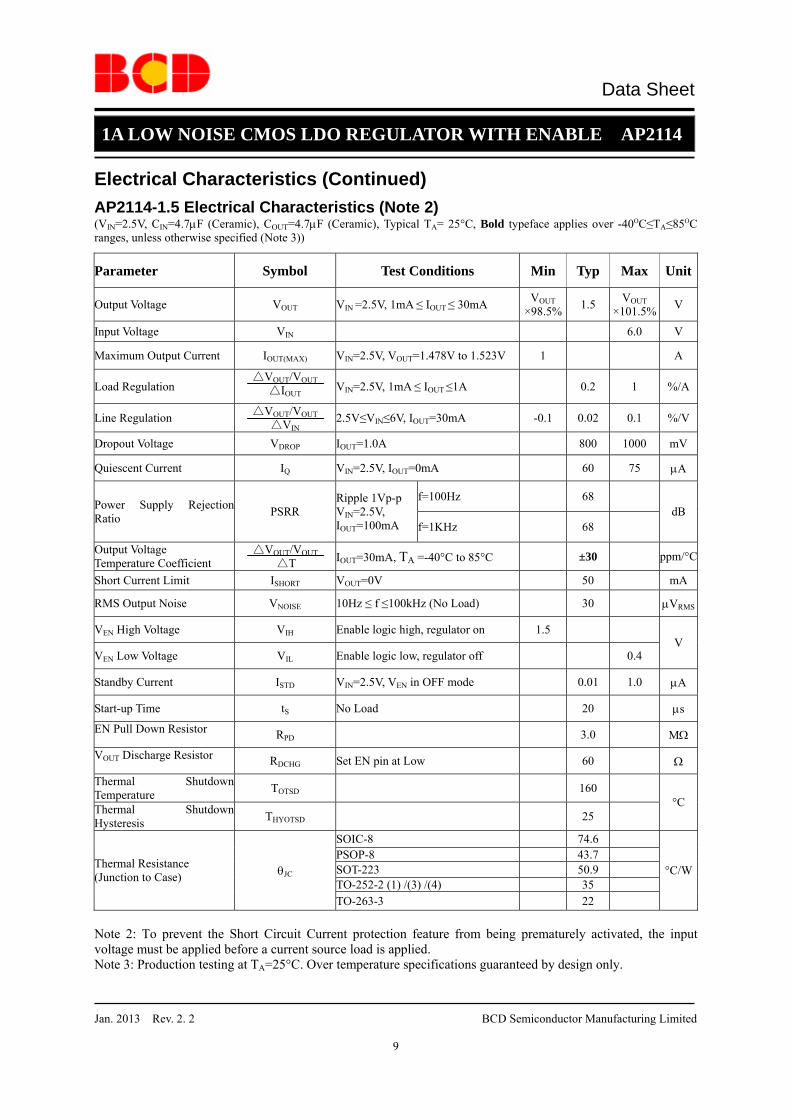
Electrical Characteristics (Continued)
AP2114-1.5 Electrical Characteristics (Note 2) (VIN=2.5V, CIN=4.7μF (Ceramic), COUT=4.7μF (Ceramic), Typical TA= 25°C, Bold typeface applies over -40OC≤TA≤85OC ranges, unless otherwise specified (Note 3))
Parameter Symbol Test Conditions Min Typ Max Unit
Output Voltage VOUT VIN =2.5V, 1mA ≤ IOUT ≤ 30mA VOUT ×98.5% 1.5 VOUT
×101.5% V
Input Voltage VIN 6.0 V
Maximum Output Current IOUT(MAX) VIN=2.5V, VOUT=1.478V to 1.523V 1 A
Load Regulation △VOUT/VOUT
I△ OUT VIN=2.5V, 1mA ≤ IOUT ≤1A 0.2 1 %/A
Line Regulation △VOUT/VOUT V△ IN
2.5V≤VIN≤6V, IOUT=30mA -0.1 0.02 0.1 %/V
Dropout Voltage VDROP IOUT=1.0A 800 1000 mV
Quiescent Current IQ VIN=2.5V, IOUT=0mA 60 75 μA
Power Supply RejectionRatio PSRR
Ripple 1Vp-p VIN=2.5V, IOUT=100mA
f=100Hz 68 dB
f=1KHz 68
Output Voltage Temperature Coefficient
△VOUT/VOUT T△ IOUT=30mA, TA =-40°C to 85°C ±30 ppm/°C
Short Current Limit ISHORT VOUT=0V 50 mA
RMS Output Noise VNOISE 10Hz ≤ f ≤100kHz (No Load) 30 μVRMS
VEN High Voltage VIH Enable logic high, regulator on 1.5 V
VEN Low Voltage VIL Enable logic low, regulator off 0.4
Standby Current ISTD VIN=2.5V, VEN in OFF mode 0.01 1.0 μA
Start-up Time tS No Load 20 μs
EN Pull Down Resistor RPD 3.0 MΩ
VOUT Discharge Resistor RDCHG Set EN pin at Low 60 Ω Thermal ShutdownTemperature TOTSD 160
°C Thermal ShutdownHysteresis THYOTSD 25
Thermal Resistance (Junction to Case) θJC
SOIC-8 74.6
°C/WPSOP-8 43.7 SOT-223 50.9 TO-252-2 (1) /(3) /(4) 35 TO-263-3 22
Note 2: To prevent the Short Circuit Current protection feature from being prematurely activated, the input voltage must be applied before a current source load is applied. Note 3: Production testing at TA=25°C. Over temperature specifications guaranteed by design only.

Data Sheet
1A LOW NOISE CMOS LDO REGULATOR WITH ENABLE AP2114
Jan. 2013 Rev. 2. 2 BCD Semiconductor Manufacturing Limited
10
Electrical Characteristics (Continued) AP2114-1.8 Electrical Characteristics (Note 2) (VIN=2.8V, CIN=4.7μF (Ceramic), COUT=4.7μF (Ceramic), Typical TA= 25°C, Bold typeface applies over -40OC≤TA≤85OC ranges, unless otherwise specified (Note 3))
Parameter Symbol Test Conditions Min Typ Max Unit
Output Voltage VOUT VIN =2.8V, 1mA ≤ IOUT ≤ 30mA VOUT ×98.5% 1.8 VOUT
×101.5% V
Maximum Output Current IOUT(MAX) VIN=2.8V, VOUT=1.773V to 1.827V 1.0 A
Load Regulation △VOUT/VOUT I△ OUT VIN=2.8V, 1mA ≤ IOUT ≤1A 0.2 1.0 %/A
Line Regulation △VOUT/VOUT V△ IN 2.8V≤VIN≤6V, IOUT=30mA -0.1 0.02 0.1 %/V
Dropout Voltage VDROP IOUT=1.0A 500 700 mV
Quiescent Current IQ VIN=2.8V, IOUT=0mA 60 75 μA
Power Supply Rejection Ratio PSRR
Ripple 1Vp-p VIN=2.8V, IOUT=100mA
f=100Hz 68 dB
f=1KHz 68
Output Voltage Temperature Coefficient
△VOUT/VOUT T△ IOUT=30mA, TA =-40°C to 85°C ±30 ppm/°C
Short Current Limit ISHORT VOUT=0V 50 mA
RMS Output Noise VNOISE 10Hz ≤ f ≤100kHz (No load) 30 μVRMS
VEN High Voltage VIH Enable logic high, regulator on 1.5 V
VEN Low Voltage VIL Enable logic low, regulator off 0.4
Standby Current ISTD VIN=2.8V, VEN in OFF mode 0.01 1.0 μA
Start-up Time tS No Load 20 μs
EN Pull Down Resistor RPD 3.0 MΩ
VOUT Discharge Resistor RDCHG Set EN pin at Low 60 Ω Thermal Shutdown Temperature TOTSD 160
°C Thermal Shutdown Hysteresis THYOTSD 25
Thermal Resistance (Junction to Case) θJC
SOIC-8 74.6
°C /W
PSOP-8 43.7
SOT-223 50.9
TO-252-2 (1) /(3) /(4) 35
TO-263-3 22
Note 2: To prevent the Short Circuit Current protection feature from being prematurely activated, the input voltage must be applied before a current source load is applied. Note 3: Production testing at TA=25°C. Over temperature specifications guaranteed by design only.

Data Sheet
1A LOW NOISE CMOS LDO REGULATOR WITH ENABLE AP2114
Jan. 2013 Rev. 2. 2 BCD Semiconductor Manufacturing Limited
11
Electrical Characteristics (Continued)
AP2114-2.5 Electrical Characteristics (Note 2) (VIN=3.5V, CIN=4.7μF (Ceramic), COUT=4.7μF (Ceramic), Typical TA= 25°C, Bold typeface applies over -40OC≤TA≤85OC ranges, unless otherwise specified (Note 3))
Parameter Symbol Test Conditions Min Typ Max Unit
Output Voltage VOUT VIN =3.5V, 1mA ≤ IOUT ≤ 30mA VOUT ×98.5% 2.5 VOUT
×101.5% V
Maximum Output Current IOUT(MAX) VIN=3.5V, VOUT=2.463V to 2.537V 1.0 A
Load Regulation △VOUT/VOUT
I△ OUT Vout=2.5V, VIN=Vout+1V 1mA ≤ IOUT ≤1A 0.2 1.0 %/A
Line Regulation △VOUT/VOUT
V△ IN 3.5V≤VIN≤6V, IOUT=30mA -0.1 0.02 0.1 %/V
Dropout Voltage VDROP IOUT =1A 450 750 mV
Quiescent Current IQ VIN=3.5V, IOUT=0mA 60 80 μA
Power Supply Rejection Ratio PSRR
Ripple 1Vp-p VIN=3.5V, IOUT=100mA
f=100Hz 65 dB
f=1KHz 65
Output Voltage Temperature Coefficient
△VOUT/VOUT T△
IOUT=30mA ±30 ppm/°C
Short Current Limit ISHORT VOUT=0V 50 mA
RMS Output Noise VNOISE 10Hz ≤ f ≤100kHz 30 μVRMS
VEN High Voltage VIH Enable logic high, regulator on 1.5 V
VEN Low Voltage VIL Enable logic low, regulator off 0.4
Standby Current ISTD VIN=3.5V, VEN in OFF mode 0.01 1.0 μA
Start-up Time tS No Load 20 μs
EN Pull Down Resistor RPD 3.0 MΩ
VOUT Discharge Resistor RDCHG Set EN pin at Low 60 Ω Thermal Shutdown Temperature TOTSD 160
°C Thermal Shutdown Hysteresis THYOTSD 25
Thermal Resistance (Junction to Case) θJC
SOIC-8 74.6
°C /W
PSOP-8 43.7
SOT-223 50.9
TO-252-2 (1) /(3) /(4) 35
TO-263-3 22 Note 2: To prevent the Short Circuit Current protection feature from being prematurely activated, the input voltage must be applied before a current source load is applied. Note 3: Production testing at TA=25°C. Over temperature specifications guaranteed by design only.

Data Sheet
1A LOW NOISE CMOS LDO REGULATOR WITH ENABLE AP2114
Jan. 2013 Rev. 2. 2 BCD Semiconductor Manufacturing Limited
12
Electrical Characteristics (Continued)
AP2114-3.3 Electrical Characteristics (Note 2) (VIN=4.3V, CIN=4.7μF (Ceramic), COUT=4.7μF (Ceramic), Typical TA= 25°C, Bold typeface applies over -40OC≤TA≤85OC ranges, unless otherwise specified (Note 3))
Parameter Symbol Test Conditions Min Typ Max Unit
Output Voltage VOUT VIN =4.3V, 1mA ≤ IOUT ≤ 30mA VOUT ×98.5% 3.3 VOUT
×101.5% V
Maximum Output Current IOUT(MAX) VIN =4.3V, VOUT=3.25V to 3.35V 1.0 A
Load Regulation △VOUT/VOUT I△ OUT VIN=4.3V, 1mA ≤ IOUT ≤1A 0.2 1.0 %/A
Line Regulation △VOUT/VOUT V△ IN 4.3V≤VIN≤6V, IOUT=30mA -0.1 0.02 0.1 %/V
Dropout Voltage VDROP IOUT=1A 450 750 mV
Quiescent Current IQ VIN=4.3V, IOUT=0mA 65 90 μA
Power Supply RejectionRatio PSRR
Ripple 1Vp-p VIN=4.3V, IOUT=100mA
f=100Hz 65 dB
f=1KHz 65 Output Voltage Temperature Coefficient
△VOUT/VOUT △T IOUT=30mA ±30 ppm/°C
Short Current Limit ISHORT VOUT=0V 50 mA
RMS Output Noise VNOISE 10Hz ≤ f ≤100kHz (No load) 30 μVRMS
VEN High Voltage VIH Enable logic high, regulator on 1.5 V
VEN Low Voltage VIL Enable logic low, regulator off 0.4
Standby Current ISTD VIN=4.3V, VEN in OFF mode 0.01 1.0 μA
Start-up Time tS No Load 20 μs
EN Pull Down Resistor RPD 3.0 MΩ
VOUT Discharge Resistor RDCHG Set EN pin at Low 60 Ω Thermal Shutdown Temperature TOTSD 160
°C Thermal ShutdownHysteresis THYOTSD 25
Thermal Resistance (Junction to Case) θJC
SOIC-8 74.6
°C/W
PSOP-8 43.7
SOT-223 50.9
TO-252-2 (1) /(3) /(4) 35
TO-263-3 22
Note 2: To prevent the Short Circuit Current protection feature from being prematurely activated, the input voltage must be applied before a current source load is applied. Note 3: Production testing at TA=25°C. Over temperature specifications guaranteed by design only.
Data Sheet
1A LOW NOISE CMOS LDO REGULATOR WITH ENABLE AP2114
Jan. 2013 Rev. 2. 2 BCD Semiconductor Manufacturing Limited
13
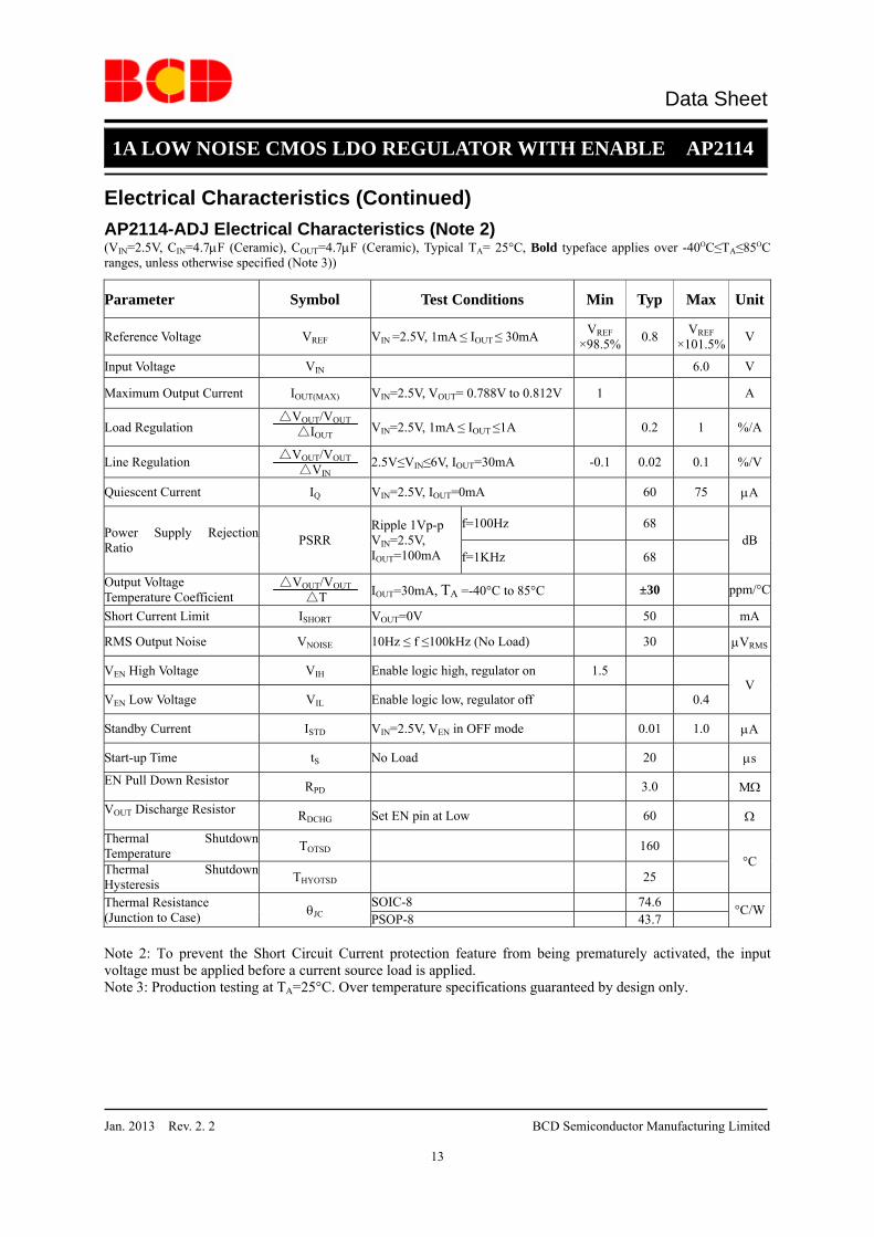
Electrical Characteristics (Continued)
AP2114-ADJ Electrical Characteristics (Note 2) (VIN=2.5V, CIN=4.7μF (Ceramic), COUT=4.7μF (Ceramic), Typical TA= 25°C, Bold typeface applies over -40OC≤TA≤85OC ranges, unless otherwise specified (Note 3))
Parameter Symbol Test Conditions Min Typ Max Unit
Reference Voltage VREF VIN =2.5V, 1mA ≤ IOUT ≤ 30mA VREF ×98.5% 0.8 VREF
×101.5% V
Input Voltage VIN 6.0 V
Maximum Output Current IOUT(MAX) VIN=2.5V, VOUT= 0.788V to 0.812V 1 A
Load Regulation △VOUT/VOUT
I△ OUT VIN=2.5V, 1mA ≤ IOUT ≤1A 0.2 1 %/A
Line Regulation △VOUT/VOUT V△ IN
2.5V≤VIN≤6V, IOUT=30mA -0.1 0.02 0.1 %/V
Quiescent Current IQ VIN=2.5V, IOUT=0mA 60 75 μA
Power Supply RejectionRatio PSRR
Ripple 1Vp-p VIN=2.5V, IOUT=100mA
f=100Hz 68 dB
f=1KHz 68
Output Voltage Temperature Coefficient
△VOUT/VOUT T△ IOUT=30mA, TA =-40°C to 85°C ±30 ppm/°C
Short Current Limit ISHORT VOUT=0V 50 mA
RMS Output Noise VNOISE 10Hz ≤ f ≤100kHz (No Load) 30 μVRMS
VEN High Voltage VIH Enable logic high, regulator on 1.5 V
VEN Low Voltage VIL Enable logic low, regulator off 0.4
Standby Current ISTD VIN=2.5V, VEN in OFF mode 0.01 1.0 μA
Start-up Time tS No Load 20 μs EN Pull Down Resistor RPD 3.0 MΩ
VOUT Discharge Resistor RDCHG Set EN pin at Low 60 Ω Thermal ShutdownTemperature TOTSD 160
°C Thermal Shutdown Hysteresis THYOTSD 25
Thermal Resistance (Junction to Case) θJC SOIC-8 74.6 °C/W
PSOP-8 43.7 Note 2: To prevent the Short Circuit Current protection feature from being prematurely activated, the input voltage must be applied before a current source load is applied. Note 3: Production testing at TA=25°C. Over temperature specifications guaranteed by design only.

Data Sheet
1A LOW NOISE CMOS LDO REGULATOR WITH ENABLE AP2114
Jan. 2013 Rev. 2. 2 BCD Semiconductor Manufacturing Limited
14
Typical Performance Characteristics
Figure 4. Ground Current vs. Output Current Figure 5. Ground Current vs. Output Current
Figure 6. Ground Current vs. Output Current Figure 7. Ground Current vs. Output Current
0.0 0.2 0.4 0.6 0.8 1.00
50
100
150
200
250
300
350
400
Continuous Airflow 10scfm
TA=-40OC TA=25OC TA=85OC
AP2114_1.8VVIN=2.8VCIN=4.7μFCOUT=4.7μF
Gro
und
Cur
rent
(μA
)
Output Current (A)
0.0 0.2 0.4 0.6 0.8 1.00
50
100
150
200
250
300
350
400
Continuous Airflow 10scfm
TA=-40OC
TA=25OC
TA=85OC
AP2114_2.5VVIN=3.5VCIN=4.7μFCOUT=4.7μF
Gro
und
Cur
rent
(μA)
Output Current (A)
0.0 0.2 0.4 0.6 0.8 1.00.0
50.0
100.0
150.0
200.0
250.0
300.0
350.0
400.0
450.0
500.0
Continuous Airflow 10scfm
AP2114_3.3V
TA=-40OC
TA=25OC
TA=85OC
VIN=4.3V
Gro
und
Cur
rent
(μA)
Output Current (A)
0.0 0.2 0.4 0.6 0.8 1.00
50
100
150
200
250
300
350
400
450
500AP2114_1.2V
TA=-40OC
TA=25OC
TA=85OC
VIN=2.5V
Gro
und
Cur
rent
(μA)
Output Current (A)
Continuous Airflow 10scfm
Data Sheet
1A LOW NOISE CMOS LDO REGULATOR WITH ENABLE AP2114
Jan. 2013 Rev. 2. 2 BCD Semiconductor Manufacturing Limited
15
Typical Performance Characteristics (Continued)
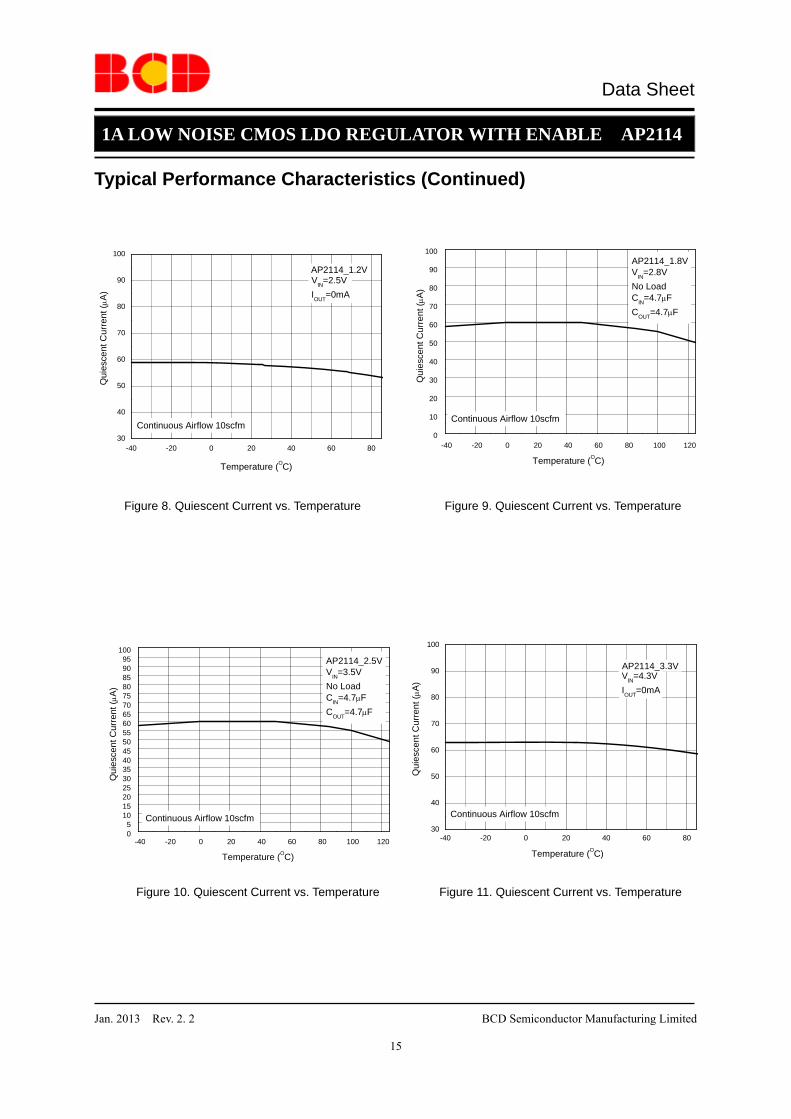
Figure 8. Quiescent Current vs. Temperature Figure 9. Quiescent Current vs. Temperature
Figure 10. Quiescent Current vs. Temperature Figure 11. Quiescent Current vs. Temperature
-40 -20 0 20 40 60 8030
40
50
60
70
80
90
100
Continuous Airflow 10scfm
VIN=2.5VIOUT=0mA
AP2114_1.2V
Qui
esce
nt C
urre
nt (μ
A)
Temperature (OC)
-40 -20 0 20 40 60 80 100 1200
10
20
30
40
50
60
70
80
90
100
Continuous Airflow 10scfm
AP2114_1.8VVIN=2.8VNo LoadCIN=4.7μFCOUT=4.7μF
Qui
esce
nt C
urre
nt (μ
A)
Temperature (OC)
-40 -20 0 20 40 60 8030
40
50
60
70
80
90
100
Continuous Airflow 10scfm
VIN=4.3VIOUT=0mA
AP2114_3.3V
Qui
esce
nt C
urre
nt (μ
A)
Temperature (OC)-40 -20 0 20 40 60 80 100 120
05
101520253035404550556065707580859095
100
Continuous Airflow 10scfm
AP2114_2.5VVIN=3.5VNo LoadCIN=4.7μFCOUT=4.7μF
Qui
esce
nt C
urre
nt (μ
A)
Temperature (OC)
Data Sheet
1A LOW NOISE CMOS LDO REGULATOR WITH ENABLE AP2114
Jan. 2013 Rev. 2. 2 BCD Semiconductor Manufacturing Limited
16
Typical Performance Characteristics (Continued)
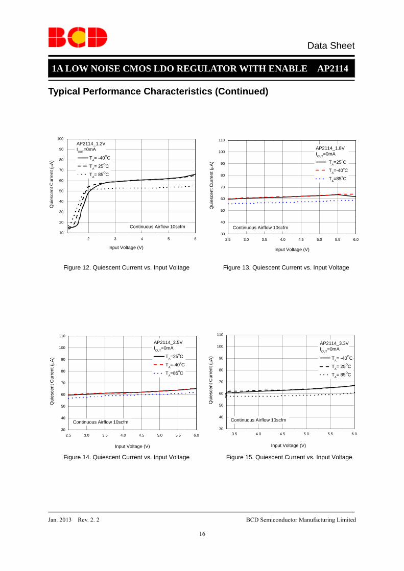
Figure 12. Quiescent Current vs. Input Voltage Figure 13. Quiescent Current vs. Input Voltage
Figure 14. Quiescent Current vs. Input Voltage Figure 15. Quiescent Current vs. Input Voltage
2 3 4 5 610
20
30
40
50
60
70
80
90
100
Continuous Airflow 10scfm
TA= -40OC
TA= 25OC
TA= 85OC
AP2114_1.2VIOUT=0mA
Qui
esce
nt C
urre
nt (μ
A)
Input Voltage (V)
3.5 4.0 4.5 5.0 5.5 6.030
40
50
60
70
80
90
100
110
Continuous Airflow 10scfm
AP2114_3.3VIOUT=0mA
Qui
esce
nt C
urre
nt (μ
A)
Input Voltage (V)
TA= -40OC
TA= 25OC
TA= 85OC
2.5 3.0 3.5 4.0 4.5 5.0 5.5 6.030
40
50
60
70
80
90
100
110
Continuous Airflow 10scfm
Qui
esce
nt C
urre
nt (μ
A)
Input Voltage (V)
AP2114_1.8VIOUT=0mA
TA=25oC
TA=-40oC
TA=85oC
2.5 3.0 3.5 4.0 4.5 5.0 5.5 6.030
40
50
60
70
80
90
100
110
Continuous Airflow 10scfm
Qui
esce
nt C
urre
nt (μ
A)
Input Voltage (V)
AP2114_2.5VIOUT=0mA
TA=25oC
TA=-40oC
TA=85oC
Data Sheet
1A LOW NOISE CMOS LDO REGULATOR WITH ENABLE AP2114
Jan. 2013 Rev. 2. 2 BCD Semiconductor Manufacturing Limited
17
Typical Performance Characteristics (Continued)
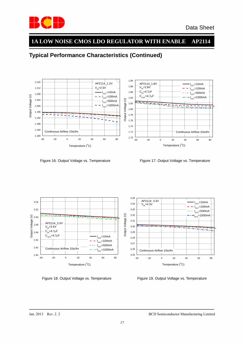
Figure 16. Output Voltage vs. Temperature Figure 17. Output Voltage vs. Temperature
Figure 18. Output Voltage vs. Temperature Figure 19. Output Voltage vs. Temperature
-40 -20 0 20 40 60 801.180
1.184
1.188
1.192
1.196
1.200
1.204
1.208
1.212
1.216
Continuous Airflow 10scfm
AP2114_1.2V
Out
put V
olta
ge (V
)
Temperature (OC)
IOUT=10mA IOUT=100mA IOUT=500mA IOUT=1000mA
VIN=2.5V
-40 -20 0 20 40 60 802.40
2.42
2.44
2.46
2.48
2.50
2.52
2.54
Continuous Airflow 10scfm
IOUT=10mA IOUT=100mA IOUT=500mA IOUT=1000mA
AP2114_2.5VVIN=3.5VCIN=4.7μFCOUT=4.7μFO
utpu
t Vol
tage
(V)
Temperature (OC)
-40 -20 0 20 40 60 803.25
3.26
3.27
3.28
3.29
3.30
3.31
3.32
3.33
3.34
3.35
Continuous Airflow 10scfm
AP2114_3.3VVIN=4.3V
Out
put V
olta
ge (V
)
Temperature (OC)
IOUT=10mA IOUT=100mA IOUT=500mAIOUT=1000mA
-40 -20 0 20 40 60 801.70
1.72
1.74
1.76
1.78
1.80
1.82
1.84
1.86
1.88
1.90
Continuous Airflow 10scfm
IOUT=10mA IOUT=100mA IOUT=500mA IOUT=1000mA
AP2114_1.8VVIN=2.8VCIN=4.7μFCOUT=4.7μF
Out
put V
olta
ge (V
)
Temperature (OC)

Data Sheet
1A LOW NOISE CMOS LDO REGULATOR WITH ENABLE AP2114
Jan. 2013 Rev. 2. 2 BCD Semiconductor Manufacturing Limited
18
Typical Performance Characteristics (Continued)
Figure 20. Output Voltage vs. Input Voltage Figure 21. Output Voltage vs. Input Voltage
Figure 22. Output Voltage vs. Input Voltage Figure 23. Output Voltage vs. Input Voltage
0.5 1.0 1.5 2.0 2.5 3.0 3.5 4.0 4.5 5.0 5.5 6.00.0
0.5
1.0
1.5
2.0
2.5
3.0
3.5
4.0
Continuous Airflow 10scfm
TA=-40OC
TA=25OC
TA=85OC
AP2114_3.3V
Out
put V
olta
ge (V
)
Input Voltage (V)
CIN=4.7μF COUT=4.7μFIOUT=10mA
0.5 1.0 1.5 2.0 2.5 3.0 3.5 4.0 4.5 5.0 5.5 6.00.0
0.2
0.4
0.6
0.8
1.0
1.2
1.4
1.6
1.8
2.0
Continuous Airflow 10scfm
Out
put V
olta
ge (V
)
Input Voltage (V)
AP2114_1.8V TA=-40oC
TA=25oC
TA=85oC CIN=4.7μF COUT=4.7μF IOUT=10mA
1 2 3 4 5 60.0
0.2
0.4
0.6
0.8
1.0
1.2
1.4
1.6
Continuous Airflow 10scfm
TA=-40OC
TA=25OC
TA=85OC
AP2114_1.2V
Out
put V
olta
ge (V
)
Input Voltage (V)
CIN=4.7μF COUT=4.7μFIOUT=10mA
1 2 3 4 5 6 7
0.0
0.5
1.0
1.5
2.0
2.5
Continuous Airflow 10scfm
AP2114_2.5VCIN=4.7μFCOUT=4.7μFIOUT=10mA
TA=-40OC
TA=25OC
TA=85OC
Out
put V
olta
ge (V
)
Input Voltage (V)

Data Sheet
1A LOW NOISE CMOS LDO REGULATOR WITH ENABLE AP2114
Jan. 2013 Rev. 2. 2 BCD Semiconductor Manufacturing Limited
19
Typical Performance Characteristics (Continued)
Figure 24. Output Voltage vs. Output Current Figure 25. Output Voltage vs. Output Current
Figure 26. Output Voltage vs. Output Current Figure 27. Output Voltage vs. Output Current
0.0 0.2 0.4 0.6 0.8 1.01.150
1.155
1.160
1.165
1.170
1.175
1.180
1.185
1.190
1.195
1.200
1.205
1.210
Continuous Airflow 10scfm
AP2114_1.2V VIN=2.5V
Out
put V
olta
ge (V
)
Output Current (A)
TA=-40OC
TA=25OC
TA=85OC
0.0 0.2 0.4 0.6 0.8 1.0 1.2 1.4 1.60.00
0.25
0.50
0.75
1.00
1.25
1.50
1.75
2.00
Continuous Airflow 10scfm
TA=-40OC
TA=25OC
TA=85OC
Out
put V
olta
ge (V
)
Output Current (A)
AP2114_1.8VVIN=2.8VCIN=4.7μFCOUT=4.7μF
0.0 0.2 0.4 0.6 0.8 1.0 1.2 1.40.0
0.1
0.2
0.3
0.4
0.5
0.6
0.7
0.8
0.9
1.0
1.1
1.2
1.3
Continuous Airflow 10scfm
VIN=2.5V VIN=3.3V
AP2114_1.2V
TA=25OC CIN=4.7μFCOUT=4.7μF
Out
put V
olta
ge (V
)
Output Current (A)
0.0 0.2 0.4 0.6 0.8 1.0 1.2 1.4 1.60.0
0.5
1.0
1.5
2.0
2.5
3.0
Continuous Airflow 10scfm
TA=-40OC
TA=25OC
TA=85OC
Out
put V
olta
ge (V
)
Output Current (A)
AP2114_2.5VVIN=3.5VCIN=4.7μFCOUT=4.7μF
Data Sheet
1A LOW NOISE CMOS LDO REGULATOR WITH ENABLE AP2114
Jan. 2013 Rev. 2. 2 BCD Semiconductor Manufacturing Limited
20
Typical Performance Characteristics (Continued)
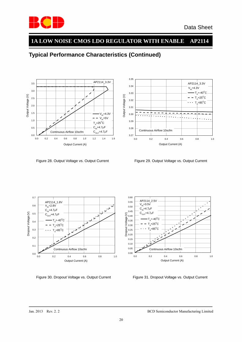
Figure 28. Output Voltage vs. Output Current Figure 29. Output Voltage vs. Output Current
Figure 30. Dropout Voltage vs. Output Current Figure 31. Dropout Voltage vs. Output Current
0.0 0.2 0.4 0.6 0.8 1.0 1.2 1.4 1.60.0
0.5
1.0
1.5
2.0
2.5
3.0
3.5
Continuous Airflow 10scfm
VIN=4.3V VIN=5V
AP2114_3.3V
TA=25OC CIN=4.7μFCOUT=4.7μF
Out
put V
olta
ge (V
)
Output Current (A)
0.0 0.2 0.4 0.6 0.8 1.03.27
3.28
3.29
3.30
3.31
3.32
3.33
3.34
3.35
Continuous Airflow 10scfm
AP2114_3.3V
TA=-40OC
TA=25OC
TA=85OC
VIN=4.3V
Out
put V
olta
ge (V
)
Output Current (A)
0.0 0.2 0.4 0.6 0.8 1.00.0
0.1
0.2
0.3
0.4
0.5
0.6
0.7
Continuous Airflow 10scfm
TA=-40OC
TA=25OC
TA=85OC
AP2114_1.8VVIN=2.8VCIN=4.7μFCOUT=4.7μF
Dro
pout
Vol
tage
(V)
Output Current (A)
0.0 0.2 0.4 0.6 0.8 1.00.00
0.05
0.10
0.15
0.20
0.25
0.30
0.35
0.40
0.45
0.50
0.55
0.60
Continuous Airflow 10scfm
TA=-40OC
TA=25OC
TA=85OC
AP2114_2.5VVIN=3.5VCIN=4.7μFCOUT=4.7μF
Dro
pout
Vol
tage
(V)
Output Current (A)

Data Sheet
1A LOW NOISE CMOS LDO REGULATOR WITH ENABLE AP2114
Jan. 2013 Rev. 2. 2 BCD Semiconductor Manufacturing Limited
21
Typical Performance Characteristics (Continued)
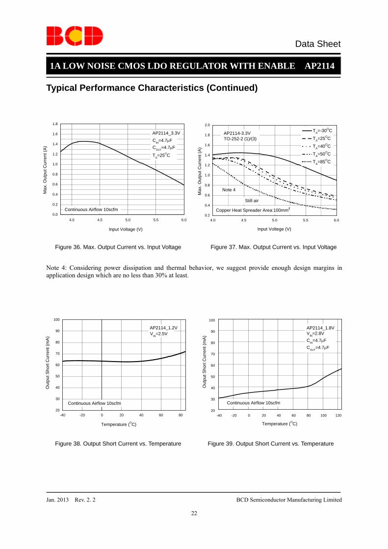
Figure 32. Dropout Voltage vs. Output Current Figure 33. Max. Output Current vs. Input Voltage
Figure 34. Max. Output Current vs. Input Voltage Figure 35. Max. Output Current vs. Input Voltage
0.0 0.2 0.4 0.6 0.8 1.00.00
0.05
0.10
0.15
0.20
0.25
0.30
0.35
0.40
0.45
0.50
0.55
0.60
Continuous Airflow 10scfm
AP2114_3.3V
TA=-40OC
TA=25OC
TA=85OC
Dro
pout
Vol
tage
(V)
Output Current (A)
CIN=4.7μF COUT=4.7μF
2.0 2.5 3.0 3.5 4.0 4.5 5.0 5.5 6.00.0
0.2
0.4
0.6
0.8
1.0
1.2
1.4
1.6
1.8
2.0
Continuous Airflow 10scfm
Max
. Out
put C
urre
nt (A
)
Input Voltage (V)
AP2114_1.8VCIN=4.7μFCOUT=4.7μFVOUT=1.8X(1+1.5%)
3.0 3.5 4.0 4.5 5.0 5.5 6.00.0
0.2
0.4
0.6
0.8
1.0
1.2
1.4
1.6
1.8
2.0
Continuous Airflow 10scfm
Max
. Out
put C
urre
nt (A
)
Input Voltage (V)
AP2114_2.5VCIN=4.7μFCOUT=4.7μFVOUT=2.5X(1+1.5%)
2.0 2.5 3.0 3.5 4.0 4.5 5.0 5.5 6.00.0
0.2
0.4
0.6
0.8
1.0
1.2
1.4
1.6
1.8
Continuous Airflow 10scfm
AP2114_1.2V
Max
. Out
put C
urre
nt (A
)
Input Voltage (V)
TA=25OCCIN=4.7μFCOUT=4.7μF
Data Sheet
1A LOW NOISE CMOS LDO REGULATOR WITH ENABLE AP2114
Jan. 2013 Rev. 2. 2 BCD Semiconductor Manufacturing Limited
22
Typical Performance Characteristics (Continued)
Figure 36. Max. Output Current vs. Input Voltage Figure 37. Max. Output Current vs. Input Voltage
Note 4: Considering power dissipation and thermal behavior, we suggest provide enough design margins in application design which are no less than 30% at least.
Figure 38. Output Short Current vs. Temperature Figure 39. Output Short Current vs. Temperature
4.0 4.5 5.0 5.5 6.00.0
0.2
0.4
0.6
0.8
1.0
1.2
1.4
1.6
1.8
Continuous Airflow 10scfm
AP2114_3.3V
Max
. Out
put C
urre
nt (A
)
Input Voltage (V)
CIN=4.7μFCOUT=4.7μF
TA=25OC
-40 -20 0 20 40 60 8020
30
40
50
60
70
80
90
100
Continuous Airflow 10scfm
VIN=2.5V
Out
put S
hort
Cur
rent
(mA)
Temperature (OC)
AP2114_1.2V
-40 -20 0 20 40 60 80 100 12020
30
40
50
60
70
80
90
100
Continuous Airflow 10scfm
AP2114_1.8VVIN=2.8VCIN=4.7μFCOUT=4.7μF
Out
put S
hort
Cur
rent
(mA)
Temperature (OC)
4.0 4.5 5.0 5.5 6.00.2
0.4
0.6
0.8
1.0
1.2
1.4
1.6
1.8
2.0
AP2114-3.3VTO-252-2 (1)/(3)
Max
. Out
put C
urre
nt (A
)
Input Voltege (V)
TA=-30OC
TA=25OC
TA=40OC
TA=50OC
TA=85OC
Copper Heat Spreader Area:100mm2
Still air
Note 4
Data Sheet
1A LOW NOISE CMOS LDO REGULATOR WITH ENABLE AP2114
Jan. 2013 Rev. 2. 2 BCD Semiconductor Manufacturing Limited
23
Typical Performance Characteristics (Continued)
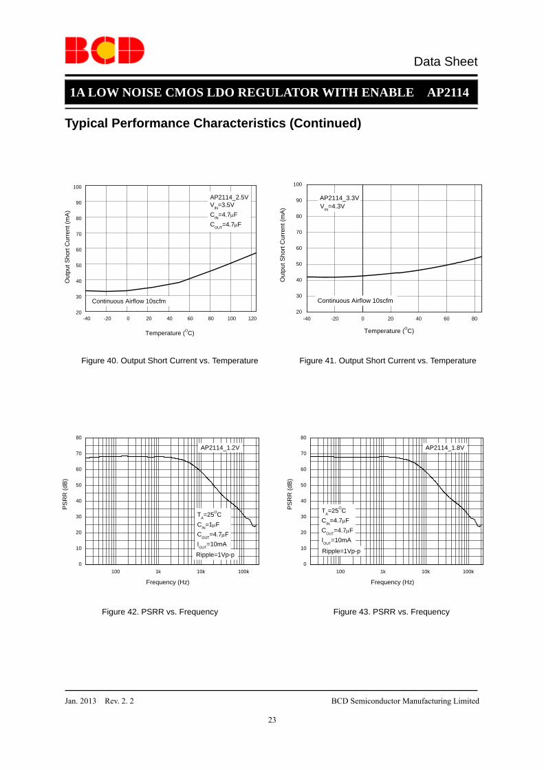
Figure 40. Output Short Current vs. Temperature Figure 41. Output Short Current vs. Temperature
Figure 42. PSRR vs. Frequency Figure 43. PSRR vs. Frequency
-40 -20 0 20 40 60 80 100 12020
30
40
50
60
70
80
90
100
Continuous Airflow 10scfm
AP2114_2.5VVIN=3.5VCIN=4.7μFCOUT=4.7μF
Out
put S
hort
Cur
rent
(mA
)
Temperature (OC)
-40 -20 0 20 40 60 8020
30
40
50
60
70
80
90
100
Continuous Airflow 10scfm
VIN=4.3V AP2114_3.3V
Out
put S
hort
Cur
rent
(mA)
Temperature (OC)
100 1k 10k 100k0
10
20
30
40
50
60
70
80
AP2114_1.2V
TA=25OCCIN=1μFCOUT=4.7μFIOUT=10mA
PSR
R (d
B)
Frequency (Hz)
Ripple=1Vp-p
100 1k 10k 100k0
10
20
30
40
50
60
70
80
AP2114_1.8V
TA=25OCCIN=4.7μFCOUT=4.7μFIOUT=10mA
PSR
R (d
B)
Frequency (Hz)
Ripple=1Vp-p

Data Sheet
1A LOW NOISE CMOS LDO REGULATOR WITH ENABLE AP2114
Jan. 2013 Rev. 2. 2 BCD Semiconductor Manufacturing Limited
24
Typical Performance Characteristics (Continued)
Figure 44. PSRR vs. Frequency Figure 45. PSRR vs. Frequency
0A
1A CIN=4.7μFCOUT=4.7μF
Figure 46. Load Transient
100 1k 10k 100k0
10
20
30
40
50
60
70
80
AP2114_2.5V
TA=25OCCIN=4.7μFCOUT=4.7μFIOUT=10mA
PSR
R (d
B)
Frequency (Hz)
Ripple=1Vp-p
100 1k 10k 100k0
10
20
30
40
50
60
70
80
IOUT=10mA IOUT=100mA
AP2114_3.3V TA=25OCCIN=1μFCOUT=4.7μF
PS
RR
(dB
)
Frequency (Hz)
Ripple=1Vp-p
Data Sheet
1A LOW NOISE CMOS LDO REGULATOR WITH ENABLE AP2114
Jan. 2013 Rev. 2. 2 BCD Semiconductor Manufacturing Limited
25
Typical Application
Figure 47. Typical Application of AP2114
Data Sheet
1A LOW NOISE CMOS LDO REGULATOR WITH ENABLE AP2114
Jan. 2013 Rev. 2. 2 BCD Semiconductor Manufacturing Limited
26
Mechanical Dimensions SOT-223 Unit: mm(inch)
3.30
0(0.
130)
3.70
0(0.
146)
6.70
0(0.
264)
7.30
0(0.
287)
2.900(0.114)3.100(0.122)
0.610(0.024)
0.810(0.032)2.300(0.091)
TYP
6.300(0.248)6.700(0.264)
1.750(0.069)TYP
4.500(0.177)
4.700(0.185)
0.020(0.001)
0.100(0.004)
1.520(0.060)
1.800(0.071)1.500(0.059)1.700(0.067)
0.250(0.010)
0.350(0.014)
0.250(0.010)
0° 10°
0.900(0.035)MIN
Data Sheet
1A LOW NOISE CMOS LDO REGULATOR WITH ENABLE AP2114
Jan. 2013 Rev. 2. 2 BCD Semiconductor Manufacturing Limited
27
Mechanical Dimensions (Continued) TO-252-2 (1) Unit: mm(inch)
1.35
0(0.
053)
1.65
0(0.
065)
0.60
0(0.
024)
0.90
0(0.
035)
3.80
0REF
(0.1
50R
EF)
4.80
0(0.
189)
6.50
0(0.
256)
1.40
0(0.
055)
1.78
0(0.
070)
9.50
0(0.
374)
9.90
0(0.
390)
2.55
0(0.
100)
2.90
0(0.
114)
5.45
0(0.
215)
6.25
0(0.
246)

Data Sheet
1A LOW NOISE CMOS LDO REGULATOR WITH ENABLE AP2114
Jan. 2013 Rev. 2. 2 BCD Semiconductor Manufacturing Limited
28
Mechanical Dimensions (Continued) TO-252-2 (3) Unit: mm(inch)
1.29±0.1
2.90
0RE
F
1.40
0(0.
055)
1.70
0(0.
067)
0.470(0.019)0.600(0.024)
59
089.
800(
0.38
6)10
.400
(0.4
09)
2.200(0.087)2.380(0.094)
0.900(0.035)1.100(0.043)
4.700REF
6.500(0.256)6.700(0.264)
5.130(0.202)5.460(0.215)
0.15
0(0.
006)
0.75
0(0.
030)
6.00
0(0.
236)
6.20
0(0.
244)
0.720(0.028)0.850(0.033)
2.286(0.090)BSC
0.720(0.028)0.900(0.035)
0.90
0(0.
035)
1.25
0(0.
049)
1.80
0REF
80
0.60
0(0.
0 24)
1.00
0(0.
039)
73
95
5.25
0REF
Option 1
Option 2

Data Sheet
1A LOW NOISE CMOS LDO REGULATOR WITH ENABLE AP2114
Jan. 2013 Rev. 2. 2 BCD Semiconductor Manufacturing Limited
29
Mechanical Dimensions (Continued) TO-252-2 (4) Unit: mm(inch)

Data Sheet
1A LOW NOISE CMOS LDO REGULATOR WITH ENABLE AP2114
Jan. 2013 Rev. 2. 2 BCD Semiconductor Manufacturing Limited
30
Mechanical Dimensions (Continued) TO-263-3 Unit: mm(inch)
7°
3°7°
8.64
0(0.
340)
9.6 5
0(0.
380)
0.990(0.039)0.510(0.020)
2.540(0.100)
1.150(0.045)
9.650(0.380)
3°
14.760(0.581)
8.840(0.348)
2.640(0.104)
0.020(0.001)
8°2°
0°6°
0.380(0.015)
2.39
0(0.
094)
0.360(0.014)
2.200(0.087)
70°
10.290(0.405)
4.070(0.160)4.820(0.190)
1.390(0.055)
1.150(0.045)1.390(0.055)
2.540(0.100)
1.270(0.050)1.390(0.055)
2.69
0(0.
106)
15.740(0.620)
0.250(0.010)
2.700(0.106)
0.400(0.016)
5.60
0(0.
220)
7.420(0.292)
7.980(0.314)
2.540(0.100)2.540(0.100)
Data Sheet
1A LOW NOISE CMOS LDO REGULATOR WITH ENABLE AP2114
Jan. 2013 Rev. 2. 2 BCD Semiconductor Manufacturing Limited
31
Mechanical Dimensions (Continued) SOIC-8 Unit: mm(inch)
R0.
150(
0.00
6)
Data Sheet
1A LOW NOISE CMOS LDO REGULATOR WITH ENABLE AP2114
Jan. 2013 Rev. 2. 2 BCD Semiconductor Manufacturing Limited
32
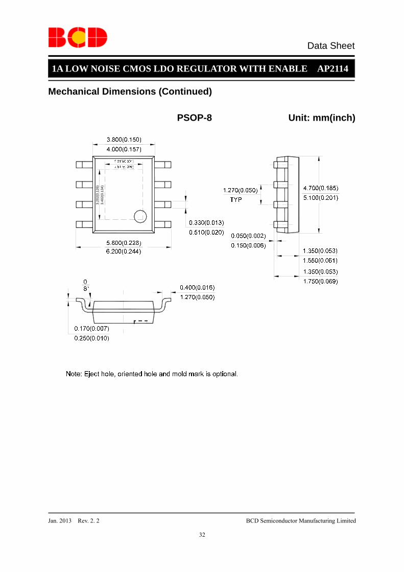
Mechanical Dimensions (Continued) PSOP-8 Unit: mm(inch)
3.20
2(0.
126)
3.40
2(0.
134)
IMPORTANT NOTICE
BCD Semiconductor Manufacturing Limited reserves the right to make changes without further notice to any products or specifi-cations herein. BCD Semiconductor Manufacturing Limited does not assume any responsibility for use of any its products for anyparticular purpose, nor does BCD Semiconductor Manufacturing Limited assume any liability arising out of the application or useof any its products or circuits. BCD Semiconductor Manufacturing Limited does not convey any license under its patent rights orother rights nor the rights of others.
- Wafer FabShanghai SIM-BCD Semiconductor Manufacturing Limited800, Yi Shan Road, Shanghai 200233, ChinaTel: +86-21-6485 1491, Fax: +86-21-5450 0008
BCD Semiconductor Manufacturing LimitedMAIN SITE
REGIONAL SALES OFFICEShenzhen OfficeShanghai SIM-BCD Semiconductor Manufacturing Co., Ltd. Shenzhen OfficeAdvanced Analog Circuits (Shanghai) Corporation Shenzhen OfficeRoom E, 5F, Noble Center, No.1006, 3rd Fuzhong Road, Futian District, Shenzhen 518026, China Tel: +86-755-8826 7951Fax: +86-755-8826 7865
Taiwan OfficeBCD Semiconductor (Taiwan) Company Limited4F, 298-1, Rui Guang Road, Nei-Hu District, Taipei, TaiwanTel: +886-2-2656 2808Fax: +886-2-2656 2806
USA OfficeBCD Semiconductor Corporation30920 Huntwood Ave. Hayward,CA 94544, U.S.ATel : +1-510-324-2988Fax: +1-510-324-2788
- IC Design GroupAdvanced Analog Circuits (Shanghai) Corporation8F, Zone B, 900, Yi Shan Road, Shanghai 200233, ChinaTel: +86-21-6495 9539, Fax: +86-21-6485 9673
BCD Semiconductor Manufacturing Limited
http://www.bcdsemi.com
BCD Semiconductor Manufacturing Limited
IMPORTANT NOTICE
BCD Semiconductor Manufacturing Limited reserves the right to make changes without further notice to any products or specifi-cations herein. BCD Semiconductor Manufacturing Limited does not assume any responsibility for use of any its products for anyparticular purpose, nor does BCD Semiconductor Manufacturing Limited assume any liability arising out of the application or useof any its products or circuits. BCD Semiconductor Manufacturing Limited does not convey any license under its patent rights orother rights nor the rights of others.
- Wafer FabShanghai SIM-BCD Semiconductor Manufacturing Co., Ltd.800 Yi Shan Road, Shanghai 200233, ChinaTel: +86-21-6485 1491, Fax: +86-21-5450 0008
MAIN SITE
REGIONAL SALES OFFICEShenzhen OfficeShanghai SIM-BCD Semiconductor Manufacturing Co., Ltd., Shenzhen OfficeUnit A Room 1203, Skyworth Bldg., Gaoxin Ave.1.S., Nanshan District, Shenzhen,China Tel: +86-755-8826 7951Fax: +86-755-8826 7865
Taiwan OfficeBCD Semiconductor (Taiwan) Company Limited4F, 298-1, Rui Guang Road, Nei-Hu District, Taipei, TaiwanTel: +886-2-2656 2808Fax: +886-2-2656 2806
USA OfficeBCD Semiconductor Corp.30920 Huntwood Ave. Hayward,CA 94544, USATel : +1-510-324-2988Fax: +1-510-324-2788
- HeadquartersBCD Semiconductor Manufacturing LimitedNo. 1600, Zi Xing Road, Shanghai ZiZhu Science-based Industrial Park, 200241, ChinaTel: +86-21-24162266, Fax: +86-21-24162277