Embed Size (px)
Citation preview
International Journal of Scientific & Engineering Research, Volume 5, Issue 5, May-2014 757 ISSN 2229-5518
IJSER © 2014 http://www.ijser.org
Low Quiescent Current High Performance Capacitor-free LDO Regulator with Optimal
Power using CMOS Multi-threshold Transistors
Sivasundar M, Krithiga S
Abstract—The main objective of the project is to design an output capacitor-free Low-Dropout Regulator (LDO) using a class-AB operational amplifier and an Assistant Push-Pull Output Stage (APPOS) circuit with multi-threshold transistors. This is done to enable fast-transient response with ultra-low power dissipation. The APPOS circuit will be designed to deliver an extra current that is directly proportional to the output current of the class-AB operational amplifier. This results in the complete separate optimization of the small-signal and large-signal responses of LDO. Thus, without the utilization of area-consuming on-chip capacitors, transient response of LDO can be improved performance wise. The proposed LDO regulator will be designed to use adaptive biasing circuit to provide better transient response compared to the existing LDO regulator. The proposed LDO will be implemented in 90nm CMOS technology with multi threshold devices to improve the slew rate and low power consumption with tradeoff.
Index Terms— Output Capacitor-free, LDO, Push-Pull, multi-threshold, slew rate, transient response, low power, tradeoff.
————————————————————
1 INTRODUCTION
Nmost electronic systems, voltage regulation is required for various functions. Today’s complex electronic systems are requiring greater
regulating performance, higher efficiency and less number of components. This voltage regulation is obtained with help of voltage regulators. This regulator may be a simple feed-forward design or may include negative feedback control loops. Present integrated circuit and power package technology has produced IC voltage regulators which can ease the task of regulated power supply design, provide the performance required and remain cost effective
Low-Dropout regulators (LDOs) are essential parts of power management systems that provide clean voltage supply rails. On-chip output capacitor less LDOs could be adjacent to individual circuit blocks to optimize the power requirements of each circuit block independently, which will improve the overall performance of systems in system-on chip designs.
———————————————— • Sivasundar M is currently pursuing masters degree program in
VLSI design in SRM University, India, pincode:603203 E-mail: [email protected]
• Krithiga S is currently working as Assistant Professor in Department of Electronics and Communication engineering in SRM University, India, pincode:603203. E-mail: [email protected]
Meanwhile, output capacitor-free LDOs can greatly reduce the area of the printed circuit board by removing large off-chip output capacitors Hence, output capacitor-free LDOs are widely used in handheld products powered by Li battery due to their low-noise characteristics and few external components.
For LDO regulator design, the main issue is to minimize the quiescent current and dropout voltage to increase power efficiency. This should be done while maintaining good regulation and a fast response time. But, reduction in value of quiescent current results in circumstantial reduction in transient response of LDO due to change in the slew rate limit at the output resistor pMOSFET power transistor since slew rate dominates the transient response of LDO. This condition can be avoided by using various methods. The typical method used is to increase the size of MOSFETs that drive the pMOSFET power transistor
As mentioned above, usage of the increased size MOSFETs leads to large bias currents. Since bias currents are proportional to the transconductance, large value of transconductance leads to reduction in the phase margin during the course when load current value is low. Since phase margin determines theGain Band-Width product (GBW), the area-consuming Miller capacitors are
I IJSER
International Journal of Scientific & Engineering Research, Volume 5, Issue 5, May-2014 758 ISSN 2229-5518
IJSER © 2014 http://www.ijser.org
utilized for the reduction of GBW required for stability requirement.
Now according to the recent research works done in LDO, the utilization of direct voltage-spike detection circuit in LDO is performed resulting in slew rate enhancement which leads to improvement in transient response. Though above method is advantageous, it requires additional resistors and capacitors. These lead to large chip area and the performances of LDO may degrade. To overcome these drawbacks, an LDO with Assistant Push-Pull Output Stage (APPOS) is utilized.
For the enhancement of slew rate also with low-power consumption, a class-AB operational amplifier is used. The APPOS circuit serves as a plug-in module and consists of four main circuits. Moreover, it can deliver extra current which is proportional to the output current of the class-AB operational amplifier to get the desired slew rate. This operation can be automatically switched on and off during the transient state.
Meanwhile, since the APPOS circuit is normally off in steady state, it does not affect the small-signal response as well. The combination of the class-AB operational amplifier and APPOS circuit results in the complete breakage of dependence between the small-signal and large-signal responses. With the gate– drain capacitance functioning as the Miller capacitor, the small-signal response such as GBW and phase margin can be optimized. Finally, the large-signal response, particularly the slew rate, could be optimized independently from the small-signal response. As a result, the transient performance of LDO is improved significantly without requiring an area-consuming on-chip capacitor anymore.
In adaptively biased low-dropout regulator [2], high loop bandwidth, fast load transient responses, high power supply rejection, and low output impedance is achieved with high-precision low-voltage adaptively biased low dropout regulator. To reduce the required minimum load current, multistage output capacitor-free low-dropout regulator is stabilized by Miller compensation and Q-reduction techniques. Adaptive biasing is achieved by using direct current feedback from a simple current mirror.
In Low-Dropout Regulator with Direct Voltage-Spike Detection [3], Output-Capacitorless LDO Regulator is proposed with direct voltage-spike detection circuit. Capacitive coupling is used in this voltage-spike detection circuit. There is an occurrence of rapid transient voltage at the LDO
output which is used by the detection circuit for the bias current increase at the moment This helps in slew rate improvement happening at the gate of power transistor such that the transient response of LDO is also enhanced
2 SYSTEM MODEL In conventional op-amp design, transient response depends on slew rate which is proportional to bias current(Ibias). Thus high Ibias gives fast transient response. Trans conductance gmα (Ibias )1/2 andGain – Bandwidth GBW α gm. The values of gm, GBW increase with high Ibias. To obtain low gm, area consuming miller capacitances must be used in turn reducing GBW. Usage of these capacitances leads to high quiescent current and increased silicon area.
To solve this problem, the class-AB operational amplifier is used here. The transconductance of this op-amp is also proportional to the square root of the bias current, which can be very low. The slew rate is not limited by the bias current as the conventional operational amplifier. Thus class-AB op-amp is used here since it has low transconductance, high slew rate and low quiescent current.
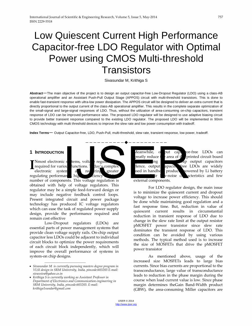
The LDO core circuit [1] consists of power transistor Mp and class-AB operational amplifier comprising of 14 other transistors MA1-MA14. Two flipped voltage follower cells consisting of MA3−MA8 act as level shifters for MA1 and MA2
.MA11and MA13 are the output stage of the class-AB operational amplifier.
The adaptive biasing circuit [1] is utilized here to extend the GBW at heavy load. Delivery of maximum current by LDO reduces gain of power stage thus decrease in GBW value.The adaptivebiasing circuit is utilized to counteract the decrease ofGBW, where VB1 and VB2 are the constant bias voltages, Vdrive connects gate of Mp and MB1. There is Ibias current source in biasing circuit. This source can improve the bias current in core circuit in turn increasing gm1. Thus GBW is improved at heavy load since GBW α gm1 .
In steady state, flipped voltage followers force equal Vgs for MA1-MA4. Hence MA1-MA4 have equal bias currents. In transient state, when Iload suddenly increases, Vout drops rapidly. Flipped voltage followers make constant Vgs for MA3
andMA4. This makes the gate–source voltage of MA2 increase while the gate–source voltage of MA1 decreases by the same amount. There is rapid increase in current through MA2, leading to MA13 pulling down the gate voltage of MP momentarily.
IJSER
International Journal of Scientific & Engineering Research, Volume 5, Issue 5, May-2014 759 ISSN 2229-5518
IJSER © 2014 http://www.ijser.org
Fig. 1. LDO core circuit with Adaptive Biasing Circuit
Similarly,when the Iload suddenly
decreases, the current through MA1 increases rapidly. This results in immediate push up of the gate voltage of MP byMA11. Hence, in both scenarios, slew rateimproves drastically. The settling time of LDO can also be greatly reduced.
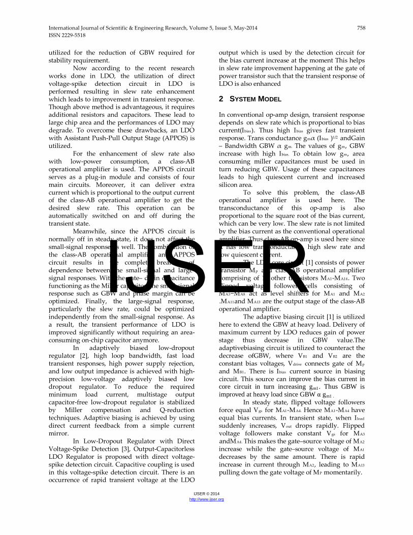
3 PROPOSED METHODOLOGY The main function of class-AB operational amplifier is to enhance slew rate. This enhanced values and results are only limited. The best solution for this problem is the utilization of Assistant Push-pull output stage (APPOS) which enhances the slew rate further and also makes small-signal and large-signal responses of LDO to be completely independent. The APPOS circuit contains overshoot/undershoot detection circuit and related driving circuit.
Fig. 2. Block Diagram of LDO with APPOS
This LDO consists of a class-AB operational amplifier and Assistant Push-Pull
Output Stage(APPOS)[1] which in turn comprises of Overshoot and Undershoot detection circuits and driving circuits. Class-AB op-amp has a differential amplifier part which is used to compute the difference between Reference voltage and the output voltage given as feedback. Overshoot detection circuit detects if Vout>Vref and Undershoot detection happens if Vout<Vref.. Driving circuits are used to push/pull the Vout value and regulate it to the value of Vref.
The circuit in figure 3 consists of power transistor Mp and class-AB operational amplifier comprising of 14 other transistors MA1-MA14. MA1−MA4 transistors act as differential amplifier for difference calculation between Vout and Vref. Mp,
MA11 and MA13 are the output stage of the proposed LDO. Two complementary current comparators composed of MC1−MC4 are designed to detect the overshoot and undershoot conditions. VPand VNare the gate voltages of MA11 and MA13 respectively. Vover and Vunder arevoltages used to indicate overshoot and undershoot conditions. The driving circuit is composed of MC5 − MC10. MC5 and MC6 acting as two switches controlled by Vover and Vunder respectively
When load current Iload varies, there is a change in output voltage Vout which is compared with Vref i.e Vout – Vref value is found by the differential amplifier stage in error amplifier. Depending on the value of the difference, we have two operations in this proposed circuit. They are (i) Overshoot detection condition (ii) Undershoot detection condition.
Fig. 3. Schematic of LDO with APPOS circuit
IJSER
International Journal of Scientific & Engineering Research, Volume 5, Issue 5, May-2014 760 ISSN 2229-5518
IJSER © 2014 http://www.ijser.org
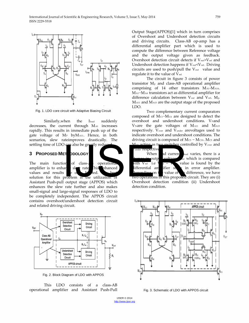
Fig.4. Schematic of Overshoot Detection Condition
When Iload suddenly drops, Vout rises rapidly, and the current through MA11 increases while that through MA13 reduces dramatically. Thus, both VPand VNdecrease abruptly. Consequently, MC1 is forced to the deep linear region, and Vover is abruptly pushed up close to Vin. Similarly, when Iload suddenly increases, Vout decreases rapidly, and Vunder is pulled down to near ground instantaneously. Once Vover is abruptly pushed to Vin, MC5 is conducted. Since the equivalent W/Laspect ratio of MC5 is much larger than that of MC7, MC5 is pushed to the deep linear region, and the gate voltages of MC9 and MA11 are equal. The APPOS circuit injects extra current to charge the gate capacitance of MP, and the gate voltage of MPis increased to reduce Iload.
When Vout is approximately regulated back to the nominal value, Vover returns to near ground. Thus, MC5 is off, and then MC7 shuts down MC9. Although MC7 divides the current from MA9 during transient state, the current through MA9 is large following the MOS square law while the current through MC7 is constant When Vout is close to the normal value, MC5 is off with Vover back to near ground. Hence, the effect of MC7 is negligible to the performance of the LDO.
When Iload suddenly increases, Vout drops rapidly and this undershoot pulls Vunder down to near ground. Therefore, MC6 is conducted and forced to the deep linear region. This leads the gate voltage of MC10 to equal that of MA13. Then, the APPOS circuit draws out extra current to discharge the gate capacitance of MP, whose gate voltage decreases to increase Iload. The operation is automatically shut down again when Vout approximately returns to the steady state.
Fig.5. Schematic of Undershoot Detection Condition
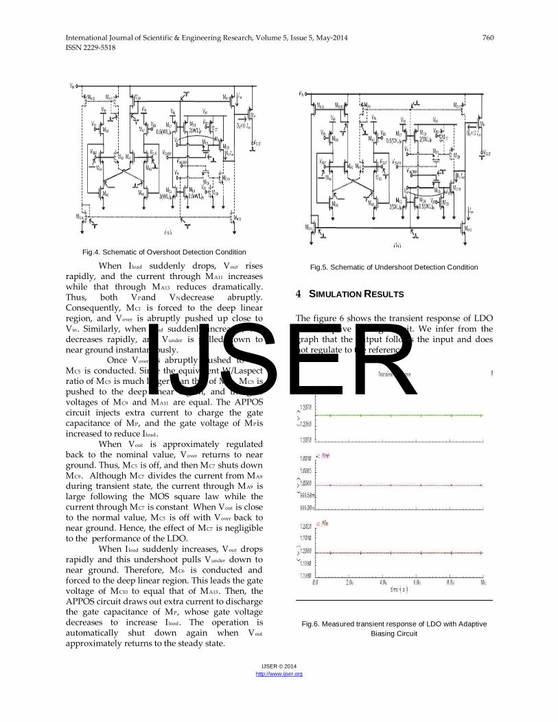
4 SIMULATION RESULTS The figure 6 shows the transient response of LDO with adaptive biasing circuit. We infer from the graph that the output follows the input and does not regulate to the reference.
Fig.6. Measured transient response of LDO with Adaptive Biasing Circuit
IJSER
International Journal of Scientific & Engineering Research, Volume 5, Issue 5, May-2014 761 ISSN 2229-5518
IJSER © 2014 http://www.ijser.org
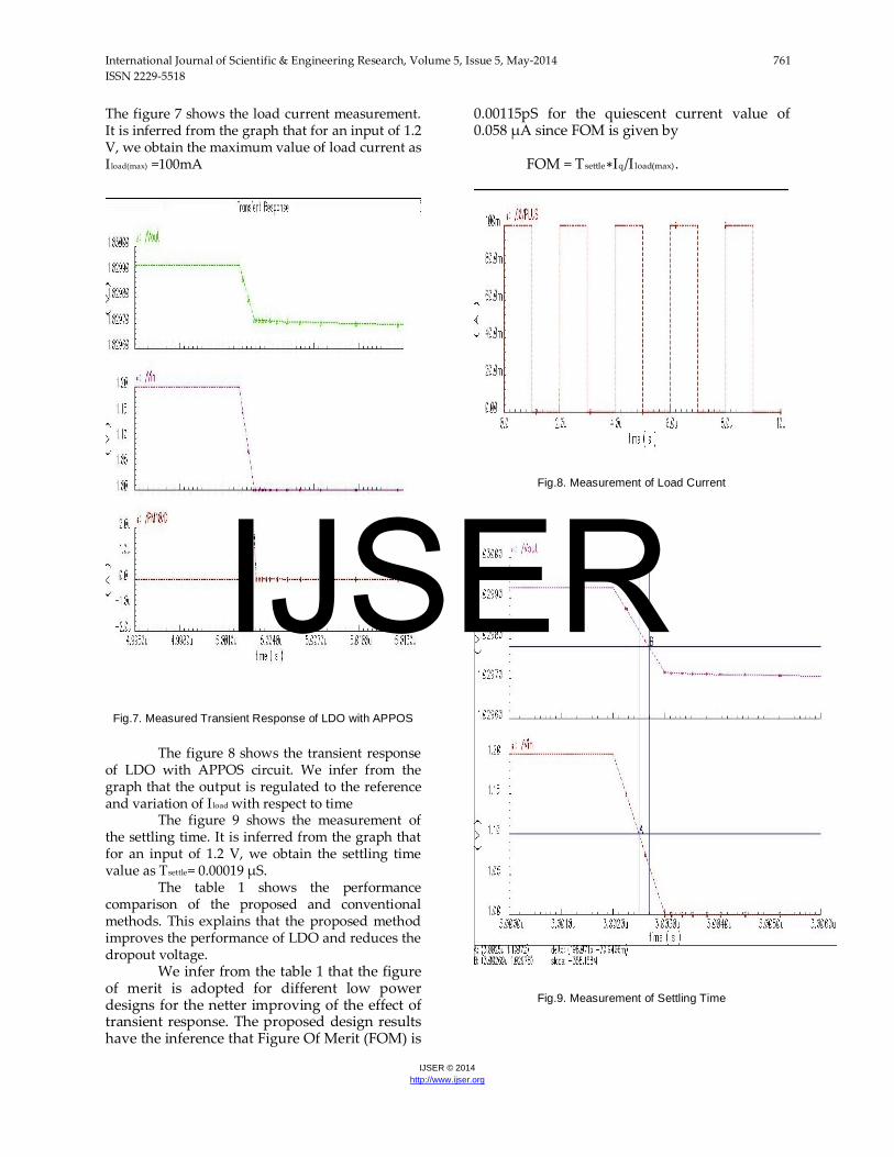
The figure 7 shows the load current measurement. It is inferred from the graph that for an input of 1.2 V, we obtain the maximum value of load current as Iload(max) =100mA
Fig.7. Measured Transient Response of LDO with APPOS
The figure 8 shows the transient response of LDO with APPOS circuit. We infer from the graph that the output is regulated to the reference and variation of Iload with respect to time
The figure 9 shows the measurement of the settling time. It is inferred from the graph that for an input of 1.2 V, we obtain the settling time value as Tsettle= 0.00019 µS.
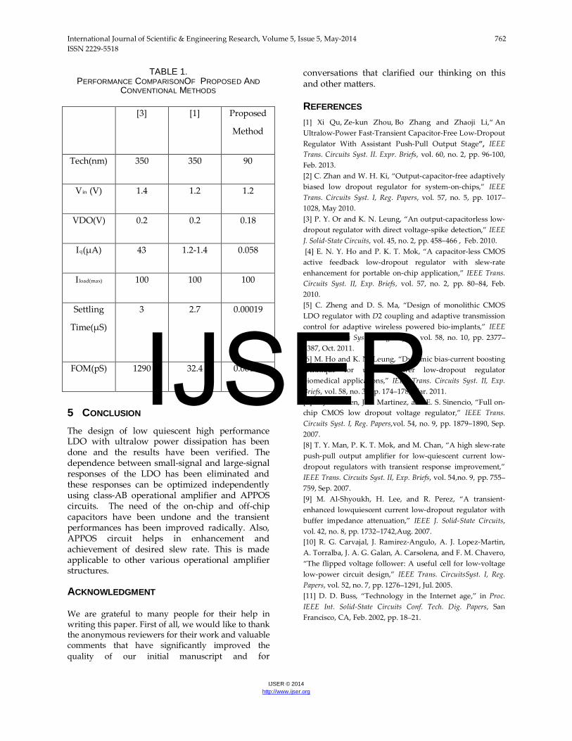
The table 1 shows the performance comparison of the proposed and conventional methods. This explains that the proposed method improves the performance of LDO and reduces the dropout voltage.
We infer from the table 1 that the figure of merit is adopted for different low power designs for the netter improving of the effect of transient response. The proposed design results have the inference that Figure Of Merit (FOM) is
0.00115pS for the quiescent current value of 0.058 µA since FOM is given by
FOM = Tsettle∗Iq/Iload(max).
Fig.8. Measurement of Load Current
Fig.9. Measurement of Settling Time
IJSER
International Journal of Scientific & Engineering Research, Volume 5, Issue 5, May-2014 762 ISSN 2229-5518
IJSER © 2014 http://www.ijser.org
TABLE 1. PERFORMANCE COMPARISONOF PROPOSED AND
CONVENTIONAL METHODS
[3] [1] Proposed
Method
Tech(nm) 350 350 90
Vin (V) 1.4 1.2 1.2
VDO(V) 0.2 0.2 0.18
Iq(µA) 43 1.2-1.4 0.058
Iload(max) 100 100 100
Settling
Time(µS)
3 2.7 0.00019
FOM(pS) 1290 32.4 0.00115
5 CONCLUSION The design of low quiescent high performance LDO with ultralow power dissipation has been done and the results have been verified. The dependence between small-signal and large-signal responses of the LDO has been eliminated and these responses can be optimized independently using class-AB operational amplifier and APPOS circuits. The need of the on-chip and off-chip capacitors have been undone and the transient performances has been improved radically. Also, APPOS circuit helps in enhancement and achievement of desired slew rate. This is made applicable to other various operational amplifier structures. ACKNOWLEDGMENT
We are grateful to many people for their help in writing this paper. First of all, we would like to thank the anonymous reviewers for their work and valuable comments that have significantly improved the quality of our initial manuscript and for
conversations that clarified our thinking on this and other matters.
REFERENCES [1] Xi Qu, Ze-kun Zhou, Bo Zhang and Zhaoji Li,“ An Ultralow-Power Fast-Transient Capacitor-Free Low-Dropout Regulator With Assistant Push-Pull Output Stage”, IEEE Trans. Circuits Syst. II. Expr. Briefs, vol. 60, no. 2, pp. 96-100, Feb. 2013. [2] C. Zhan and W. H. Ki, “Output-capacitor-free adaptively biased low dropout regulator for system-on-chips,” IEEE Trans. Circuits Syst. I, Reg. Papers, vol. 57, no. 5, pp. 1017–1028, May 2010. [3] P. Y. Or and K. N. Leung, “An output-capacitorless low-dropout regulator with direct voltage-spike detection,” IEEE J. Solid-State Circuits, vol. 45, no. 2, pp. 458–466 , Feb. 2010. [4] E. N. Y. Ho and P. K. T. Mok, “A capacitor-less CMOS active feedback low-dropout regulator with slew-rate enhancement for portable on-chip application,” IEEE Trans. Circuits Syst. II, Exp. Briefs, vol. 57, no. 2, pp. 80–84, Feb. 2010. [5] C. Zheng and D. S. Ma, “Design of monolithic CMOS LDO regulator with D2 coupling and adaptive transmission control for adaptive wireless powered bio-implants,” IEEE Trans. Circuits Syst. I, Reg. Papers, vol. 58, no. 10, pp. 2377–2387, Oct. 2011. [6] M. Ho and K. N. Leung, “Dynamic bias-current boosting technique for ultralow-power low-dropout regulator biomedical applications,” IEEE Trans. Circuits Syst. II, Exp. Briefs, vol. 58, no. 3, pp. 174–178, Mar. 2011. [7] R. J. Milliken, J. S. Martinez, and E. S. Sinencio, “Full on-chip CMOS low dropout voltage regulator,” IEEE Trans. Circuits Syst. I, Reg. Papers,vol. 54, no. 9, pp. 1879–1890, Sep. 2007. [8] T. Y. Man, P. K. T. Mok, and M. Chan, “A high slew-rate push-pull output amplifier for low-quiescent current low-dropout regulators with transient response improvement,” IEEE Trans. Circuits Syst. II, Exp. Briefs, vol. 54,no. 9, pp. 755–759, Sep. 2007. [9] M. Al-Shyoukh, H. Lee, and R. Perez, “A transient-enhanced lowquiescent current low-dropout regulator with buffer impedance attenuation,” IEEE J. Solid-State Circuits, vol. 42, no. 8, pp. 1732–1742,Aug. 2007. [10] R. G. Carvajal, J. Ramirez-Angulo, A. J. Lopez-Martin, A. Torralba, J. A. G. Galan, A. Carsolena, and F. M. Chavero, “The flipped voltage follower: A useful cell for low-voltage low-power circuit design,” IEEE Trans. CircuitsSyst. I, Reg. Papers, vol. 52, no. 7, pp. 1276–1291, Jul. 2005. [11] D. D. Buss, “Technology in the Internet age,” in Proc. IEEE Int. Solid-State Circuits Conf. Tech. Dig. Papers, San Francisco, CA, Feb. 2002, pp. 18–21.
IJSER


![Output LDO Regulators Ultra Low Quiescent Current LDO ...0 2 4 6 8 12 14 16 18 20 0 40 80 120 160 200 OUTPUT CURRENT : IOUT[mA]-40 C 25 C 125 C Total supply current vs. Load Figure](https://img.pdfslide.us/doc/110x75/61143a411c02b07ee452b42d/output-ldo-regulators-ultra-low-quiescent-current-ldo-0-2-4-6-8-12-14-16-18.jpg)