Embed Size (px)
Citation preview
1/29 www.rohm.com 2011.01 - Rev.C
© 2011 ROHM Co., Ltd. All rights reserved.
CMOS LDO Regulators for Portable Equipments 1ch 200mA CMOS LDO Regulators BUTA2WNVX series, BUTA2WHFV series
Description
BUTA2WNVX /HFV series is high-performance FULL CMOS regulator with 200-mA output, which is mounted on microminiature package SSON004X1216 (1.2 mm 1.6 mm 0.6 mm) &HVSOF5(1.6mm 1.6mm 0.6mm). It has excellent noise characteristics and load responsiveness characteristics despite its low circuit current consumption of 40 µA. It is most appropriate for various applications such as power supplies for logic IC, RF, and camera modules. Microminiature package SSON004X1216 & HVSOF5 with built-in heatsink is adopted for the package, which contributes to the space-saving design of the set.
Features
1) High-accuracy output voltage of 1% (25 mV on 1.5-V & 1.8-V products) 2) High ripple rejection: 70 dB (Typ., 1 kHz, VOUT1.8 V)) 3) Compatible with small ceramic capacitor (CIN=Co=1.0 µF) 4) Low current consumption: 40 µA 5) ON/OFF control of output voltage 6) With built-in overcurrent protection circuit and overheat protection circuit 7) With built-in output discharge circuit 8) Adopting microminiature power package SSON004X1216
Applications
Battery-powered portable equipment, etc. Line up
200 mA BUTA2WNVX / HFV series
Product Name 1.5 1.8 2.5 2.6 2.7 2.8 2.85 2.9 3.0 3.1 3.2 3.3 3.4 Package
BUTA2WNVX SSON004X1216
BUTA2WHFV HVSOF5
Model name: BHTA2W
a b
Symbol Contents
a
Specification of output voltage
Output voltage (V) Output voltage (V) Output voltage (V)
15 1.5V(Typ.) 28 2.8V(Typ.) 32 3.2V(Typ.)
18 1.8V(Typ.) 2J 2.85V(Typ.) 33 3.3V(Typ.)
25 2.5V(Typ.) 29 2.9V(Typ.) 34 3.4V(Typ.)
26 2.6V(Typ.) 30 3.0V(Typ.) - -
27 2.7V(Typ.) 31 3.1V(Typ.) - -
b Package NVX :SSON004X1216
HFV :HVSOF5
No.11020ECT01
Technical Note
2/29
BUTA2WNVX series, BUTA2WHFV series
www.rohm.com 2011.01 - Rev.C© 2011 ROHM Co., Ltd. All rights reserved.
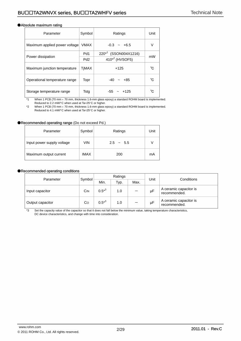
Absolute maximum rating
Parameter Symbol Ratings Unit
Maximum applied power voltage VMAX -0.3 ~ +6.5 V
Power dissipation Pd1 220*1 (SSON004X1216)
mW Pd2 410*2 (HVSOF5)
Maximum junction temperature TjMAX +125
Operational temperature range Topr -40 ~ +85
Storage temperature range Tstg -55 ~ +125
*1 When 1 PCB (70 mm 70 mm, thickness 1.6-mm glass epoxy) a standard ROHM board is implemented. Reduced to 2.2 mW/C when used at Ta=25C or higher. *2 When 1 PCB (70 mm 70 mm, thickness 1.6-mm glass epoxy) a standard ROHM board is implemented. Reduced to 4.1 mW/C when used at Ta=25C or higher.
Recommended operating range (Do not exceed Pd.)
Parameter Symbol Ratings Unit
Input power supply voltage VIN 2.5 ~ 5.5 V
Maximum output current IMAX 200 mA
Recommended operating conditions
Parameter Symbol Ratings
Unit Conditions Min. Typ. Max.
Input capacitor CIN 0.5*3 1.0 - μF A ceramic capacitor is recommended.
Output capacitor CO 0.5*3 1.0 - μF A ceramic capacitor is recommended.
*3 Set the capacity value of the capacitor so that it does not fall below the minimum value, taking temperature characteristics, DC device characteristics, and change with time into consideration.
Technical Note
3/29
BUTA2WNVX series, BUTA2WHFV series
www.rohm.com 2011.01 - Rev.C© 2011 ROHM Co., Ltd. All rights reserved.
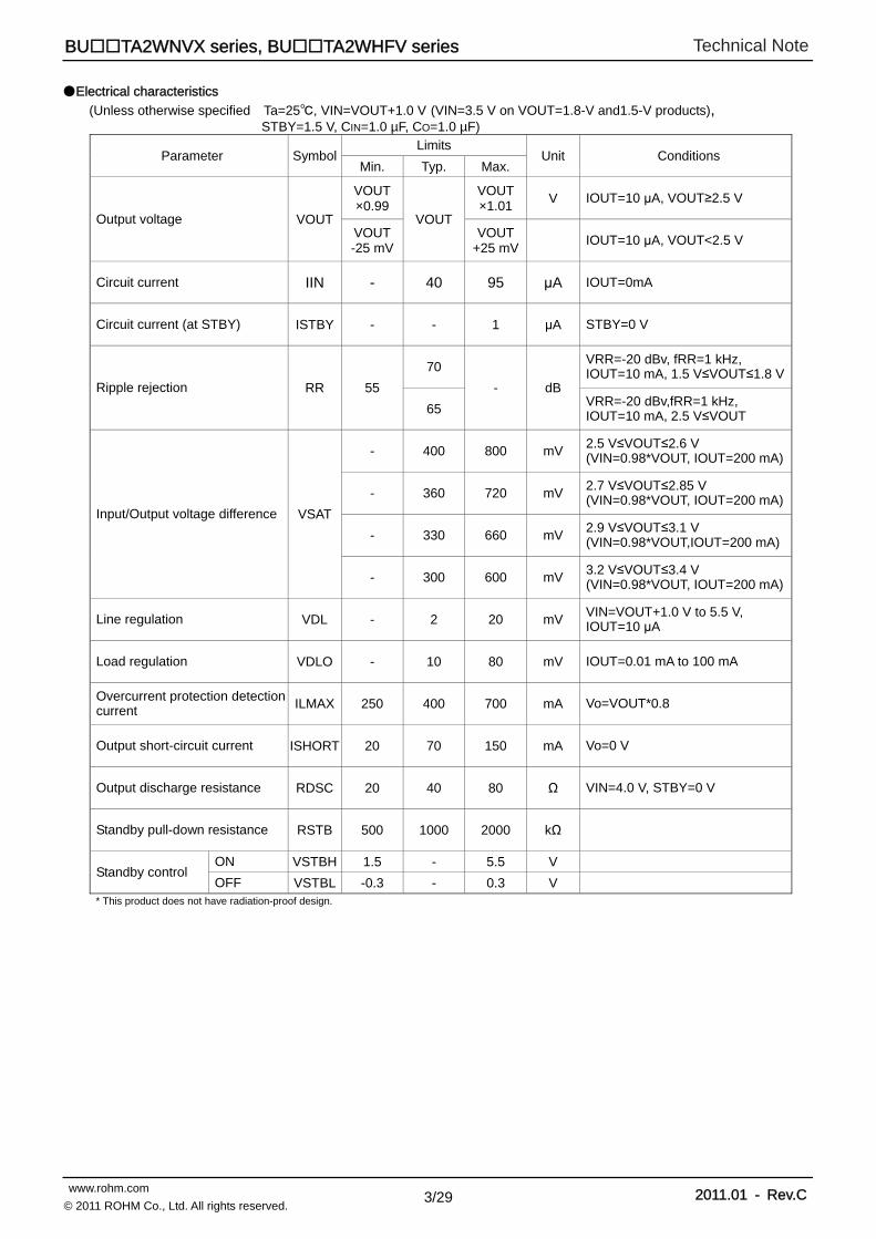
Electrical characteristics
(Unless otherwise specified Ta=25, VIN=VOUT+1.0 V (VIN=3.5 V on VOUT=1.8-V and1.5-V products), STBY=1.5 V, CIN=1.0 µF, CO=1.0 µF)
Parameter Symbol Limits
Unit Conditions Min. Typ. Max.
Output voltage VOUT
VOUT×0.99
VOUT
VOUT×1.01
V IOUT=10 μA, VOUT≥2.5 V
VOUT-25 mV
VOUT+25 mV
IOUT=10 μA, VOUT<2.5 V
Circuit current IIN - 40 95 μA IOUT=0mA
Circuit current (at STBY) ISTBY - - 1 μA STBY=0 V
Ripple rejection RR 55
70
- dB
VRR=-20 dBv, fRR=1 kHz, IOUT=10 mA, 1.5 V≤VOUT≤1.8 V
65 VRR=-20 dBv,fRR=1 kHz, IOUT=10 mA, 2.5 V≤VOUT
Input/Output voltage difference VSAT
- 400 800 mV 2.5 V≤VOUT≤2.6 V (VIN=0.98*VOUT, IOUT=200 mA)
- 360 720 mV 2.7 V≤VOUT≤2.85 V (VIN=0.98*VOUT, IOUT=200 mA)
- 330 660 mV 2.9 V≤VOUT≤3.1 V (VIN=0.98*VOUT,IOUT=200 mA)
- 300 600 mV 3.2 V≤VOUT≤3.4 V (VIN=0.98*VOUT, IOUT=200 mA)
Line regulation VDL - 2 20 mV VIN=VOUT+1.0 V to 5.5 V, IOUT=10 μA
Load regulation VDLO - 10 80 mV IOUT=0.01 mA to 100 mA
Overcurrent protection detection current ILMAX 250 400 700 mA Vo=VOUT*0.8
Output short-circuit current ISHORT 20 70 150 mA Vo=0 V
Output discharge resistance RDSC 20 40 80 Ω VIN=4.0 V, STBY=0 V
Standby pull-down resistance RSTB 500 1000 2000 kΩ
Standby control ON VSTBH 1.5 - 5.5 V
OFF VSTBL -0.3 - 0.3 V
* This product does not have radiation-proof design.
Technical Note
4/29
BUTA2WNVX series, BUTA2WHFV series
www.rohm.com 2011.01 - Rev.C© 2011 ROHM Co., Ltd. All rights reserved.
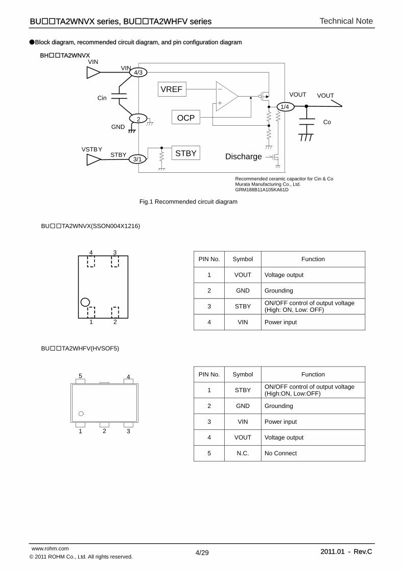
Block diagram, recommended circuit diagram, and pin configuration diagram
BUTA2WNVX(SSON004X1216)
PIN No. Symbol Function
1 VOUT Voltage output
2 GND Grounding
3 STBY ON/OFF control of output voltage (High: ON, Low: OFF)
4 VIN Power input
BUTA2WHFV(HVSOF5)
PIN No. Symbol Function
1 STBY ON/OFF control of output voltage (High:ON, Low:OFF)
2 GND Grounding
3 VIN Power input
4 VOUT Voltage output
5 N.C. No Connect
BHTA2WNVX
Fig.1 Recommended circuit diagram
Recommended ceramic capacitor for Cin & Co Murata Manufacturing Co., Ltd. GRM188B11A105KA61D
1 2
4 3
1 2 3
45
1Cin
VINVIN
GND
STBY
VOUT
VOUT
Co
VREF
OCP
STBY Discharge
VSTBY
4/3
2
1/4
3/1
Technical Note
5/29
BUTA2WNVX series, BUTA2WHFV series
www.rohm.com 2011.01 - Rev.C© 2011 ROHM Co., Ltd. All rights reserved.
Fig.4 Stability area characteristics (Example)
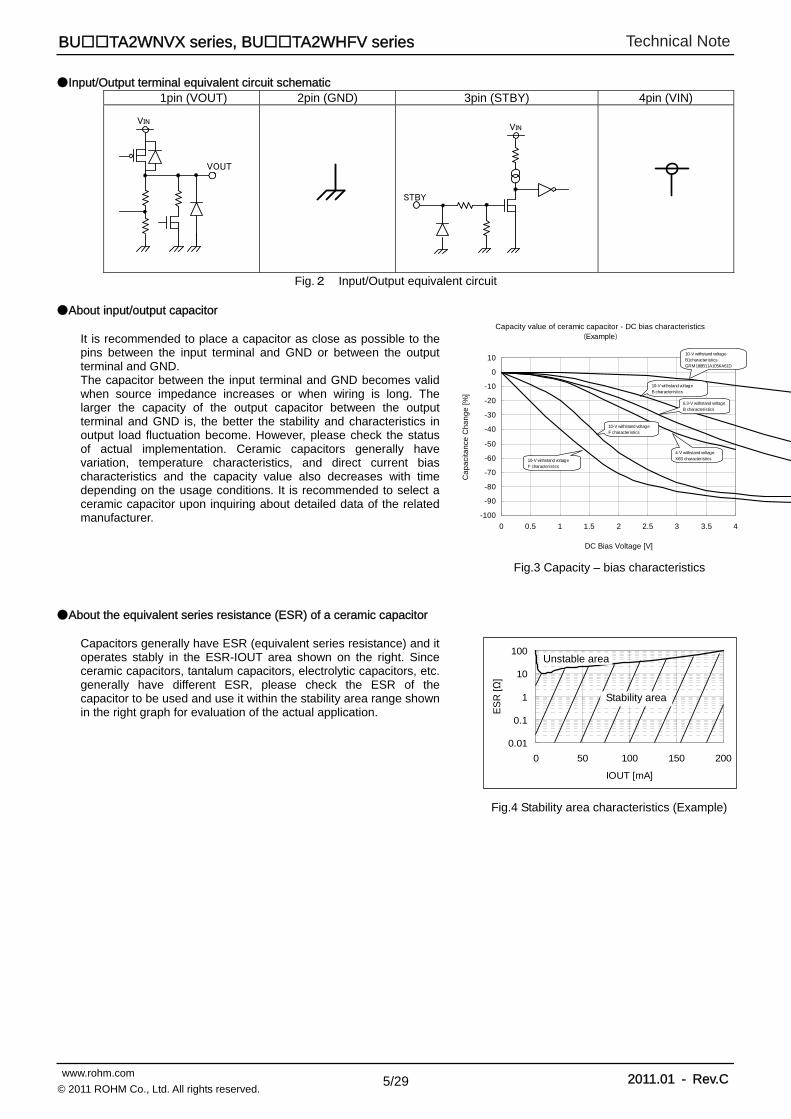
Input/Output terminal equivalent circuit schematic 1pin (VOUT) 2pin (GND) 3pin (STBY) 4pin (VIN)
VIN
STBY
Fig.2 Input/Output equivalent circuit
About input/output capacitor
It is recommended to place a capacitor as close as possible to the pins between the input terminal and GND or between the output terminal and GND. The capacitor between the input terminal and GND becomes valid when source impedance increases or when wiring is long. The larger the capacity of the output capacitor between the output terminal and GND is, the better the stability and characteristics in output load fluctuation become. However, please check the status of actual implementation. Ceramic capacitors generally have variation, temperature characteristics, and direct current bias characteristics and the capacity value also decreases with time depending on the usage conditions. It is recommended to select a ceramic capacitor upon inquiring about detailed data of the related manufacturer.
About the equivalent series resistance (ESR) of a ceramic capacitor
Capacitors generally have ESR (equivalent series resistance) and it operates stably in the ESR-IOUT area shown on the right. Since ceramic capacitors, tantalum capacitors, electrolytic capacitors, etc. generally have different ESR, please check the ESR of the capacitor to be used and use it within the stability area range shown in the right graph for evaluation of the actual application.
VOUT
VIN
Fig.3 Capacity – bias characteristics
Capacity value of ceramic capacitor - DC bias characteristics(Example)
-100
-90
-80
-70
-60
-50
-40
-30
-20
-10
0
10
0 0.5 1 1.5 2 2.5 3 3.5 4
DC Bias Voltage [V]
Ca
pa
cita
nce
Ch
an
ge
[%
]
10-V withstand voltageB1characteristicsGRM188B11A105KA61D
10-V withstand voltageB characteristics
6.3-V withstand voltageB characteristics
4-V withstand voltageX6S characteristics
10-V withstand voltageF characteristics
10-V withstand voltageF characteristics
0.01
0.1
1
10
100
0 50 100 150 200
IOUT [mA]
ES
R [Ω
]
Stability area
Unstable area
Technical Note
6/29
BUTA2WNVX series, BUTA2WHFV series
www.rohm.com 2011.01 - Rev.C© 2011 ROHM Co., Ltd. All rights reserved.
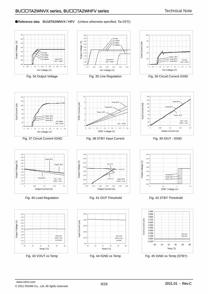
Fig. 5 Output Voltage Fig. 6 Line Regulation
Fig. 14 VOUT vs. Temp
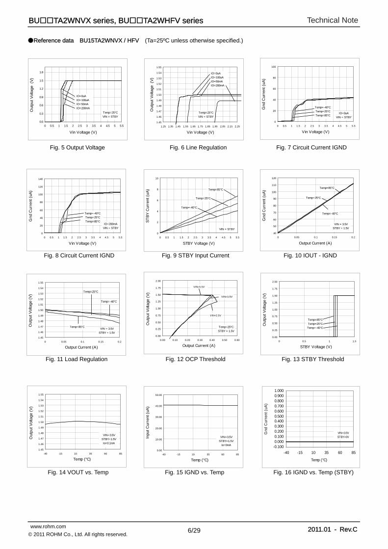
Reference data BU15TA2WNVX / HFV (Ta=25ºC unless otherwise specified.)
Fig. 7 Circuit Current IGND
Fig. 8 Circuit Current IGND Fig. 9 STBY Input Current Fig. 10 IOUT - IGND
Fig. 16 IGND vs. Temp (STBY) Fig. 15 IGND vs. Temp
Fig. 11 Load Regulation Fig. 13 STBY Threshold Fig. 12 OCP Threshold
0.0
0.3
0.6
0.9
1.2
1.5
1.8
0 0.5 1 1.5 2 2.5 3 3.5 4 4.5 5 5.5
Vin Voltage (V)
Out
put V
olta
ge (
V)
IO=0uAIO=100uAIO=50mAIO=200mA
Temp=25°CVIN = STBY
1.45
1.46
1.47
1.48
1.49
1.50
1.51
1.52
1.53
1.54
1.55
1.25 1.35 1.45 1.55 1.65 1.75 1.85 1.95 2.05 2.15 2.25
Vin Voltage (V)
Out
put V
olta
ge (
V)
IO=0uAIO=100uAIO=50mAIO=200mA
Temp=25°CVIN = STBY
0
20
40
60
80
100
0 0.5 1 1.5 2 2.5 3 3.5 4 4.5 5 5.5
Vin Voltage (V)
Gnd
Cur
rent
(uA
)
Temp=-40°CTemp=25°CTemp=85°C
IO=0uAVIN = STBY
0
20
40
60
80
100
120
140
0 0.5 1 1.5 2 2.5 3 3.5 4 4.5 5 5.5
Vin Voltage (V)
Gnd
Cur
rent
(uA
)
IO=200mAVIN = STBY
Temp=-40°CTemp=25°CTemp=85°C
0
2
4
6
8
10
0 0.5 1 1.5 2 2.5 3 3.5 4 4.5 5 5.5
STBY Voltage (V)
ST
BY
Cur
rent
(uA
)
VIN = STBY
Temp=85°C
Temp=25°C
Temp=-40°C
40
50
60
70
80
90
100
110
120
0 0.05 0.1 0.15 0.2
Output Current (A)
Gnd
Cur
rent
(uA
)
VIN = 3.5VSTBY = 1.5V
Temp=85°C
Temp=25°C
Temp=-40°C
1.45
1.46
1.47
1.48
1.49
1.50
1.51
1.52
1.53
1.54
1.55
0 0.05 0.1 0.15 0.2
Output Current (A)
Out
put V
olta
ge (
V)
VIN = 3.5VSTBY = 1.5V
Temp=-40°C
Temp=25°C
Temp=85°C
0.00
0.25
0.50
0.75
1.00
1.25
1.50
1.75
2.00
0.00 0.10 0.20 0.30 0.40 0.50 0.60
Output Current (A)
Out
put V
olta
ge (
V)
VIN=5.5V
Temp=25°CSTBY = 1.5V
VIN=3.5V
VIN=2.5V
0.00
0.25
0.50
0.75
1.00
1.25
1.50
1.75
2.00
0 0.5 1 1.5
STBY Voltage (V)
Out
put V
olta
ge (
V)
Temp=85°CTemp=25°CTemp=-40°C
1.45
1.46
1.47
1.48
1.49
1.50
1.51
1.52
1.53
1.54
1.55
-40 -15 10 35 60 85
Temp (°C)
Out
put V
olta
ge (
V)
VIN=3.5VSTBY=1.5VIo=0.1mA
0.00
10.00
20.00
30.00
40.00
50.00
-40 -15 10 35 60 85
Temp (°C)
Inpu
t Cur
rent
(uA
)
VIN=3.5VSTBY=1.5V
Io=0mA -0.1000.0000.1000.2000.3000.4000.5000.6000.7000.8000.9001.000
-40 -15 10 35 60 85
Temp (°C)
Gnd
Cur
rent
(uA
)
VIN=3.5VSTBY=0V
Technical Note
7/29
BUTA2WNVX series, BUTA2WHFV series
www.rohm.com 2011.01 - Rev.C© 2011 ROHM Co., Ltd. All rights reserved.
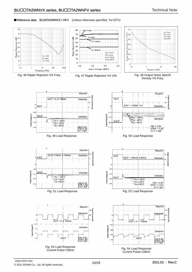
Fig. 19 Output Noise Spectral Density vs. Freq.
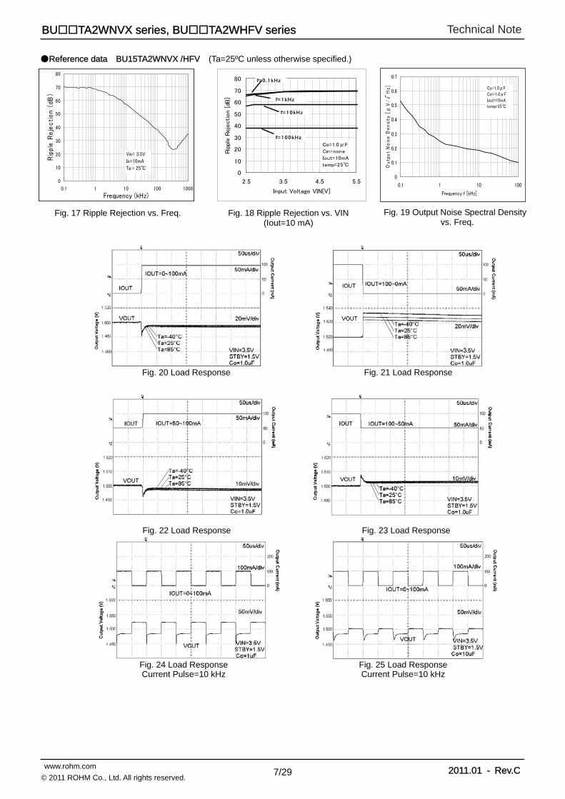
Reference data BU15TA2WNVX /HFV (Ta=25ºC unless otherwise specified.)
Fig. 18 Ripple Rejection vs. VIN (Iout=10 mA)
Fig. 17 Ripple Rejection vs. Freq.
Fig. 24 Load Response Current Pulse=10 kHz
Fig. 25 Load Response Current Pulse=10 kHz
Fig. 20 Load Response Fig. 21 Load Response
Fig. 22 Load Response Fig. 23 Load Response
0
10
20
30
40
50
60
70
80
0.1 1 10 100 1000
Frequency (kHz)
Rip
ple
Re
jec
tio
n (
dB)
Vin= 3.5V
Io=10mA
Ta = 25
0
0.1
0.2
0.3
0.4
0.5
0.6
0.7
0.1 1 10 100
Frequency f [kHz]
Ou
tpu
t N
ois
e D
en
sity
[μ
V/
√H
z] Co=1.0μFCin=1.0μFIout=10mAtemp=25
0
10
20
30
40
50
60
70
80
2.5 3.5 4.5 5.5
Input Voltage VIN[V]
Rip
ple R
eje
ction [dB
]
Co=1.0μF
Cin=none
Iout=10mA
temp=25
f=100kHz
f=10kHz
f=1kHz
f=0 .1 kHz
Technical Note
8/29
BUTA2WNVX series, BUTA2WHFV series
www.rohm.com 2011.01 - Rev.C© 2011 ROHM Co., Ltd. All rights reserved.
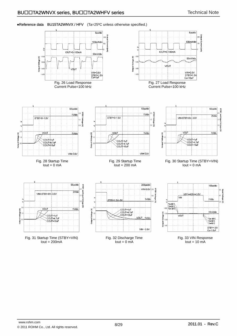
Reference data BU15TA2WNVX / HFV (Ta=25ºC unless otherwise specified.)
Fig. 29 Startup TimeIout = 200 mA
Fig. 30 Startup Time (STBY=VIN)Iout = 0 mA
Fig. 28 Startup Time Iout = 0 mA
Fig. 32 Discharge TimeIout = 0 mA
Fig. 33 VIN ResponseIout = 10 mA
Fig. 31 Startup Time (STBY=VIN) Iout = 200mA
Fig. 26 Load Response Current Pulse=100 kHz
Fig. 27 Load Response Current Pulse=100 kHz
Technical Note
9/29
BUTA2WNVX series, BUTA2WHFV series
www.rohm.com 2011.01 - Rev.C© 2011 ROHM Co., Ltd. All rights reserved.
Fig. 34 Output Voltage Fig. 35 Line Regulation
Fig. 43 VOUT vs Temp
Reference data BU18TA2WNVX / HFV (Unless otherwise specified, Ta=25)
Fig. 36 Circuit Current IGND
Fig. 38 STBY Input Current Fig. 39 IOUT - IGND
Fig. 45 IGND vs Temp (STBY)Fig. 44 IGND vs Temp
Fig. 40 Load Regulation Fig. 42 STBY ThresholdFig. 41 OCP Threshold
Fig. 37 Circuit Current IGND
0.0
0.5
1.0
1.5
2.0
2.5
3.0
3.5
0 0.5 1 1.5 2 2.5 3 3.5 4 4.5 5 5.5
Vin Voltage (V)
Out
put V
olta
ge (
V)
IO=0uAIO=100uAIO=50mAIO=200mA Temp=25°C
VIN = STBY
0
20
40
60
80
100
0 0.5 1 1.5 2 2.5 3 3.5 4 4.5 5 5.5
Vin Voltage (V)
Gnd
Cur
rent
(uA
)
Temp=-40°CTemp=25°CTemp=85°C
IO=0uAVIN = STBY
0
20
40
60
80
100
120
140
0 0.5 1 1.5 2 2.5 3 3.5 4 4.5 5 5.5
Vin Voltage (V)
Gnd
Cur
rent
(uA
)
IO=200mAVIN = STBY
Temp=-40°CTemp=25°CTemp=85°C
0
2
4
6
8
10
0 0.5 1 1.5 2 2.5 3 3.5 4 4.5 5 5.5
STBY Voltage (V)
ST
BY
Cur
rent
(uA
)
VIN = STBY
Temp=85°C
Temp=25°C
Temp=-40°C
1.75
1.76
1.77
1.78
1.79
1.80
1.81
1.82
1.83
1.84
1.85
0 0.05 0.1 0.15 0.2
Output Current (A)
Out
put V
olta
ge (
V)
VIN = 3.5VSTBY = 1.5V
Temp=-40°C
Temp=25°C
Temp=85°C
0.00
0.50
1.00
1.50
2.00
2.50
3.00
3.50
0.00 0.10 0.20 0.30 0.40 0.50 0.60
Output Current (A)
Out
put V
olta
ge (
V)
VIN=5.5V
Temp=25°CSTBY = 1.5V
VIN=3.5V
VIN=2.5V
0.00
0.50
1.00
1.50
2.00
2.50
3.00
3.50
0 0.5 1 1.5
STBY Voltage (V)
Out
put V
olta
ge (
V)
Temp=85°CTemp=25°CTemp=-40°C
1.75
1.76
1.77
1.78
1.79
1.80
1.81
1.82
1.83
1.84
1.85
-40 -15 10 35 60 85
Temp (°C)
Out
put V
olta
ge (
V)
VIN=3.5VSTBY=1.5VIo=0.1mA
0.00
10.00
20.00
30.00
40.00
50.00
-40 -15 10 35 60 85
Temp (°C)
Inpu
t Cur
rent
(uA
)
VIN=3.5VSTBY=1.5V
Io=0mA-0.1000.0000.1000.2000.3000.4000.5000.6000.7000.8000.9001.000
-40 -15 10 35 60 85
Temp (°C)
Gnd
Cur
rent
(uA
)
VIN=3.5VSTBY=0V
1.75
1.76
1.77
1.78
1.79
1.80
1.81
1.82
1.83
1.84
1.85
1.75 1.85 1.95 2.05 2.15 2.25 2.35
Vin Voltage (V)
Out
put V
olta
ge (
V)
IO=0uAIO=100uAIO=50mAIO=200mA
Temp=25°CVIN = STBY
40
50
60
70
80
90
100
110
120
0 0.05 0.1 0.15 0.2
Output Current (A)
Gnd
Cur
rent
(uA
)
VIN = 3.5VSTBY = 1.5V
Temp=85°C
Temp=25°C
Temp=-40°C
Technical Note
10/29
BUTA2WNVX series, BUTA2WHFV series
www.rohm.com 2011.01 - Rev.C© 2011 ROHM Co., Ltd. All rights reserved.
Fig. 46 Ripple Rejection VS Freq. Fig. 47 Ripple Rejection VS VIN Fig. 48 Output Noise SpectrlDensity VS Freq.
Reference data BU18TA2WNVX / HFV (Unless otherwise specified, Ta=25)
Fig. 49 Load Response
Fig. 51 Load Response Fig. 52 Load Response
Fig. 50 Load Response
Fig. 53 Load Response Current Pulse=10kHz Fig. 54 Load Response
Current Pulse=10kHz
⇔
0
10
20
30
40
50
60
70
80
0.1 1 10 100 1000
Frequency (kHz)
Rip
ple R
eje
cti
on (
dB
)
Vin= 3.5V
Io=10mA
Ta = 250
10
20
30
40
50
60
70
80
2.5 3.5 4.5 5.5
Input Voltage VIN[V]
Rip
ple R
eje
ction [dB
]
Co=1.0μF
Cin=none
Iout=10mA
temp=25
f=100kHz
f=10kHz
f=1 kHz
f=0 .1kHz
0
0.1
0.2
0.3
0.4
0.5
0.6
0.7
0.1 1 10 100
Frequency f [kHz]
Ou
tpu
t N
ois
e D
en
sity
[μ
V/
√H
z]
Co=1.0μFCin=1.0μFIout=10mAtemp=25
Technical Note
11/29
BUTA2WNVX series, BUTA2WHFV series
www.rohm.com 2011.01 - Rev.C© 2011 ROHM Co., Ltd. All rights reserved.
Reference data BU18TA2WNVX / HFV (Unless otherwise specified, Ta=25)
Fig. 55 Load Response Current Pulse=100kHz
Fig. 56 Load Response Current Pulse=100kHz
Fig. 57 Start Up Time Iout = 0mA
Fig. 58 Start Up TimeIout = 200mA
Fig. 59 Start Up Time (STBY=VIN)Iout = 0mA
Fig. 61 Discharge TimeIout = 0mA
Fig. 62 VIN ResponseIout = 10mA
Fig. 60 Start Up Time(STBY=VIN) Iout = 200mA
⇔
Technical Note
12/29
BUTA2WNVX series, BUTA2WHFV series
www.rohm.com 2011.01 - Rev.C© 2011 ROHM Co., Ltd. All rights reserved.
Fig. 63 Output Voltage Fig. 64 Line Regulation
Fig. 72 VOUT vs Temp
0.00
0.05
0.10
0.15
0.20
0.25
0.30
0.35
0.40
0.45
0.50
0 0.05 0.1 0.15 0.2
Output Current (A)
Dro
pout
Vol
tage
(V
)
VIN=0.98*VOUTSTBY=1.5V
Temp.=-40°C
Temp.=25°C
Temp.=85°C
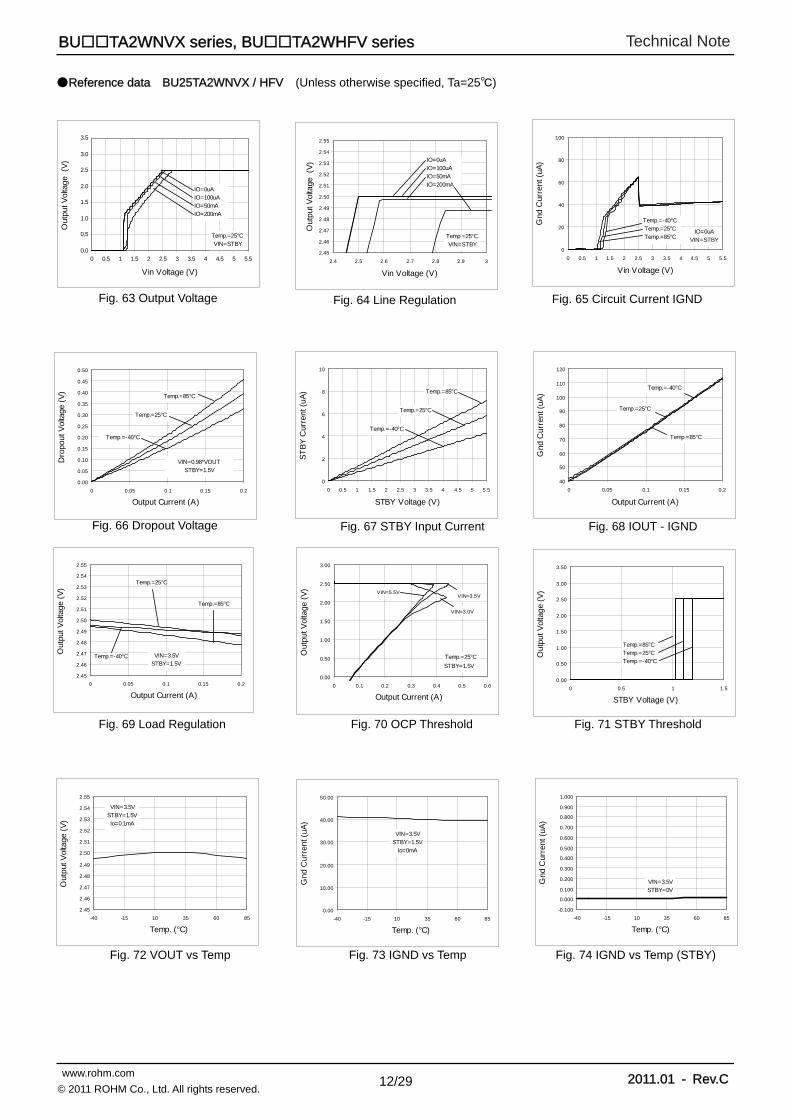
Reference data BU25TA2WNVX / HFV (Unless otherwise specified, Ta=25)
Fig. 65 Circuit Current IGND
Fig. 67 STBY Input Current Fig. 68 IOUT - IGND
Fig. 74 IGND vs Temp (STBY)Fig. 73 IGND vs Temp
Fig. 69 Load Regulation Fig. 71 STBY ThresholdFig. 70 OCP Threshold
Fig. 66 Dropout Voltage
0.0
0.5
1.0
1.5
2.0
2.5
3.0
3.5
0 0.5 1 1.5 2 2.5 3 3.5 4 4.5 5 5.5
Vin Voltage (V)
Out
put V
olta
ge (
V)
IO=0uAIO=100uAIO=50mAIO=200mA
Temp.=25°CVIN=STBY
2.45
2.46
2.47
2.48
2.49
2.50
2.51
2.52
2.53
2.54
2.55
2.4 2.5 2.6 2.7 2.8 2.9 3
Vin Voltage (V)
Out
put V
olta
ge (
V) IO=0uA
IO=100uAIO=50mAIO=200mA
Temp.=25°CVIN=STBY
0
20
40
60
80
100
0 0.5 1 1.5 2 2.5 3 3.5 4 4.5 5 5.5
Vin Voltage (V)
Gnd
Cur
rent
(uA
)
Temp.=-40°CTemp.=25°CTemp.=85°C
IO=0uAVIN=STBY
0
2
4
6
8
10
0 0.5 1 1.5 2 2.5 3 3.5 4 4.5 5 5.5
STBY Voltage (V)
ST
BY
Cur
rent
(uA
) Temp.=85°C
Temp.=25°C
Temp.=-40°C
40
50
60
70
80
90
100
110
120
0 0.05 0.1 0.15 0.2
Output Current (A)
Gnd
Cur
rent
(uA
)
Temp.=85°C
Temp.=25°C
Temp.=-40°C
0.00
0.50
1.00
1.50
2.00
2.50
3.00
0 0.1 0.2 0.3 0.4 0.5 0.6
Output Current (A)
Out
put V
olta
ge (
V) VIN=5.5V
VIN=3.5V
VIN=3.0V
Temp.=25°C
STBY=1.5V
0.00
0.50
1.00
1.50
2.00
2.50
3.00
3.50
0 0.5 1 1.5
STBY Voltage (V)
Out
put V
olta
ge (
V)
Temp.=85°CTemp.=25°CTemp.=-40°C
2.45
2.46
2.47
2.48
2.49
2.50
2.51
2.52
2.53
2.54
2.55
-40 -15 10 35 60 85
Temp. (°C)
Out
put V
olta
ge (
V)
VIN=3.5VSTBY=1.5VIo=0.1mA
0.00
10.00
20.00
30.00
40.00
50.00
-40 -15 10 35 60 85
Temp. (°C)
Gnd
Cur
rent
(uA
)
VIN=3.5VSTBY=1.5V
Io=0mA
-0.100
0.000
0.100
0.200
0.300
0.400
0.500
0.600
0.700
0.800
0.900
1.000
-40 -15 10 35 60 85
Temp. (°C)
Gnd
Cur
rent
(uA
)
VIN=3.5VSTBY=0V
2.45
2.46
2.47
2.48
2.49
2.50
2.51
2.52
2.53
2.54
2.55
0 0.05 0.1 0.15 0.2
Output Current (A)
Out
put V
olta
ge (
V)
VIN=3.5VSTBY=1.5V
Temp.=-40°C
Temp.=25°C
Temp.=85°C
Technical Note
13/29
BUTA2WNVX series, BUTA2WHFV series
www.rohm.com 2011.01 - Rev.C© 2011 ROHM Co., Ltd. All rights reserved.
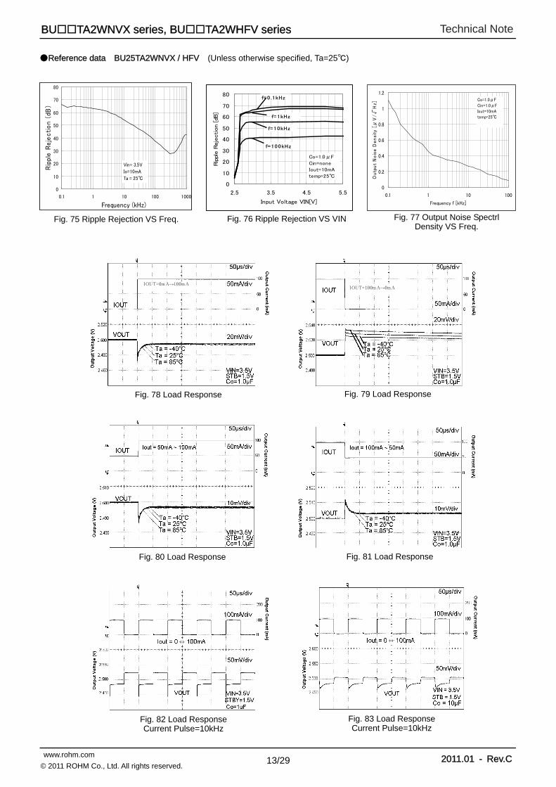
Fig. 75 Ripple Rejection VS Freq. Fig. 76 Ripple Rejection VS VIN Fig. 77 Output Noise SpectrlDensity VS Freq.
Reference data BU25TA2WNVX / HFV (Unless otherwise specified, Ta=25)
Fig. 78 Load Response
Fig. 80 Load Response Fig. 81 Load Response
Fig. 79 Load Response
Fig. 82 Load Response Current Pulse=10kHz
Fig. 83 Load Response Current Pulse=10kHz
IOUT=0m A→100m A
IOUT=100m A→0m A
⇔
⇔
0
10
20
30
40
50
60
70
80
0.1 1 10 100 1000
Frequency (kHz)
Rip
ple
Re
jec
tio
n (
dB)
Vin= 3.5V
Io=10mA
Ta = 250
10
20
30
40
50
60
70
80
2.5 3.5 4.5 5.5
Input Voltage VIN[V]
Rip
ple R
eje
ction [dB
]
Co=1.0μF
Cin=none
Iout=10mA
temp=25
f=100kHz
f=10kHz
f=1kHz
f=0 .1 kHz
0
0.2
0.4
0.6
0.8
1
1.2
0.1 1 10 100
Frequency f [kHz]
Ou
tpu
t N
ois
e D
en
sity
[μ
V/
√H
z]
Co=1.0μFCin=1.0μFIout=10mAtemp=25
Technical Note
14/29
BUTA2WNVX series, BUTA2WHFV series
www.rohm.com 2011.01 - Rev.C© 2011 ROHM Co., Ltd. All rights reserved.
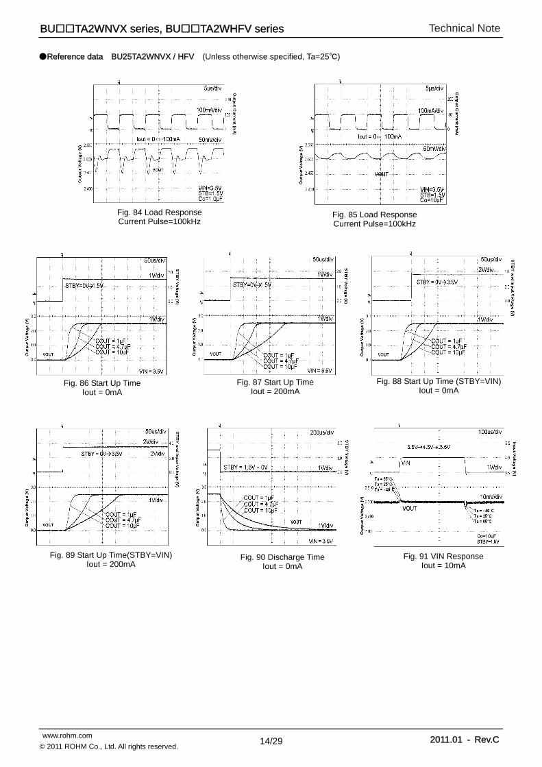
Reference data BU25TA2WNVX / HFV (Unless otherwise specified, Ta=25)
Fig. 84 Load Response Current Pulse=100kHz
Fig. 85 Load Response Current Pulse=100kHz
Fig. 86 Start Up Time Iout = 0mA
Fig. 87 Start Up TimeIout = 200mA
Fig. 88 Start Up Time (STBY=VIN)Iout = 0mA
Fig. 90 Discharge TimeIout = 0mA
Fig. 91 VIN ResponseIout = 10mA
Fig. 89 Start Up Time(STBY=VIN) Iout = 200mA
⇔
⇔
Technical Note
15/29
BUTA2WNVX series, BUTA2WHFV series
www.rohm.com 2011.01 - Rev.C© 2011 ROHM Co., Ltd. All rights reserved.
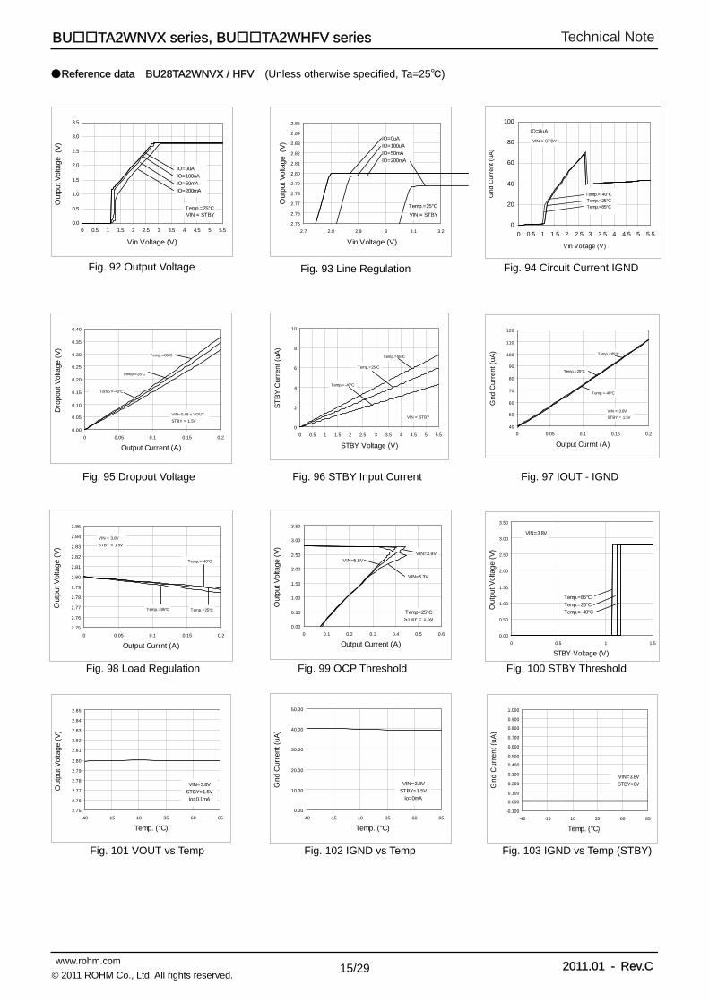
Fig. 92 Output Voltage Fig. 93 Line Regulation
Fig. 101 VOUT vs Temp
Reference data BU28TA2WNVX / HFV (Unless otherwise specified, Ta=25)
Fig. 94 Circuit Current IGND
Fig. 96 STBY Input Current Fig. 97 IOUT - IGND
Fig. 103 IGND vs Temp (STBY)Fig. 102 IGND vs Temp
Fig. 98 Load Regulation Fig. 100 STBY ThresholdFig. 99 OCP Threshold
Fig. 95 Dropout Voltage
0.0
0.5
1.0
1.5
2.0
2.5
3.0
3.5
0 0.5 1 1.5 2 2.5 3 3.5 4 4.5 5 5.5
Vin Voltage (V)
Out
put V
olta
ge (
V)
Temp.=25°C
IO=0uAIO=100uAIO=50mAIO=200mA
VIN = STBY
2.75
2.76
2.77
2.78
2.79
2.80
2.81
2.82
2.83
2.84
2.85
2.7 2.8 2.9 3 3.1 3.2
Vin Voltage (V)
Out
put V
olta
ge (
V)
Temp.=25°C
IO=0uAIO=100uAIO=50mAIO=200mA
VIN = STBY
0
20
40
60
80
100
0 0.5 1 1.5 2 2.5 3 3.5 4 4.5 5 5.5
Vin Voltage (V)
Gnd
Cur
rent
(uA
)
Temp.=-40°CTemp.=25°CTemp.=85°C
IO=0uA
VIN = STBY
0.00
0.05
0.10
0.15
0.20
0.25
0.30
0.35
0.40
0 0.05 0.1 0.15 0.2
Output Current (A)
Dro
pout
Vol
tage
(V
)
VIN=0.98 x VOUT
STBY = 1.5V
Temp.=-40°C
Temp.=25°C
Temp.=85°C
0
2
4
6
8
10
0 0.5 1 1.5 2 2.5 3 3.5 4 4.5 5 5.5
STBY Voltage (V)
ST
BY
Cur
rent
(uA
)
Temp.=85°C
Temp.=25°C
Temp.=-40°C
VIN = STBY
40
50
60
70
80
90
100
110
120
0 0.05 0.1 0.15 0.2
Output Currnt (A)
Gnd
Cur
rent
(uA
)
VIN = 3.8V
STBY = 1.5V
Temp.=85°C
Temp.=25°C
Temp.=-40°C
2.75
2.76
2.77
2.78
2.79
2.80
2.81
2.82
2.83
2.84
2.85
0 0.05 0.1 0.15 0.2
Output Currnt (A)
Out
put V
olta
ge (
V)
Temp.=-40°C
Temp.=25°CTemp.=85°C
VIN = 3.8V
STBY = 1.5V
0.00
0.50
1.00
1.50
2.00
2.50
3.00
3.50
0 0.1 0.2 0.3 0.4 0.5 0.6
Output Current (A)
Out
put V
olta
ge (
V)
VIN=5.5V
STBY = 1.5V
VIN=3.8V
VIN=3.3V
Temp=25°C
0.00
0.50
1.00
1.50
2.00
2.50
3.00
3.50
0 0.5 1 1.5
STBY Voltage (V)
Out
put V
olta
ge (
V)
VIN=3.8V
Temp.=85°CTemp.=25°CTemp.=-40°C
2.75
2.76
2.77
2.78
2.79
2.80
2.81
2.82
2.83
2.84
2.85
-40 -15 10 35 60 85
Temp. (°C)
Out
put V
olta
ge (
V)
VIN=3.8VSTBY=1.5VIo=0.1mA
0.00
10.00
20.00
30.00
40.00
50.00
-40 -15 10 35 60 85
Temp. (°C)
Gnd
Cur
rent
(uA
)
VIN=3.8VSTBY=1.5V
Io=0mA
-0.100
0.000
0.100
0.200
0.300
0.400
0.500
0.600
0.700
0.800
0.900
1.000
-40 -15 10 35 60 85
Temp. (°C)
Gnd
Cur
rent
(uA
)
VIN=3.8VSTBY=0V
Technical Note
16/29
BUTA2WNVX series, BUTA2WHFV series
www.rohm.com 2011.01 - Rev.C© 2011 ROHM Co., Ltd. All rights reserved.
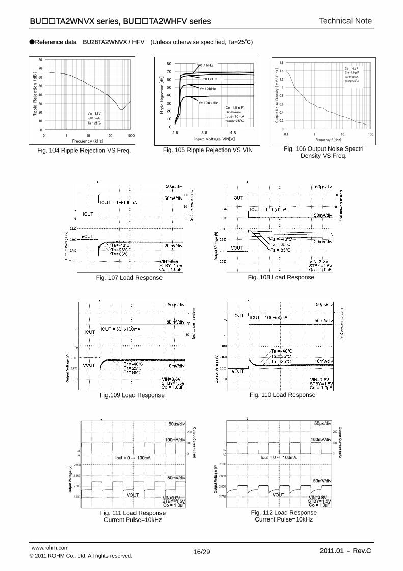
Fig. 104 Ripple Rejection VS Freq. Fig. 105 Ripple Rejection VS VIN Fig. 106 Output Noise SpectrlDensity VS Freq.
Reference data BU28TA2WNVX / HFV (Unless otherwise specified, Ta=25)
Fig. 107 Load Response
Fig.109 Load Response Fig. 110 Load Response
Fig. 108 Load Response
Fig. 111 Load Response Current Pulse=10kHz
Fig. 112 Load Response Current Pulse=10kHz
⇔
⇔
0
10
20
30
40
50
60
70
80
0.1 1 10 100 1000
Frequency (kHz)
Rip
ple R
eje
ction (
dB)
Vin= 3.8V
Io=10mA
Ta = 250
10
20
30
40
50
60
70
80
2.8 3.8 4.8
Input Voltage VIN[V]
Rip
ple R
eje
ction [dB
]
f= 1 00kHz
f=10kHz
f=1kHz
f=0 .1 kHz
Co=1.0μF
Cin=none
Iout=10mA
temp=25
0
0.2
0.4
0.6
0.8
1
1.2
1.4
1.6
0.1 1 10 100
Frequency f [kHz]
Outp
ut
Nois
e D
ensi
ty [
μV
/√
Hz] Co=1.0μF
Cin=1.0μFIout=10mAtemp=25
Technical Note
17/29
BUTA2WNVX series, BUTA2WHFV series
www.rohm.com 2011.01 - Rev.C© 2011 ROHM Co., Ltd. All rights reserved.
Reference data BU28TA2WNVX / HFV (Unless otherwise specified, Ta=25)
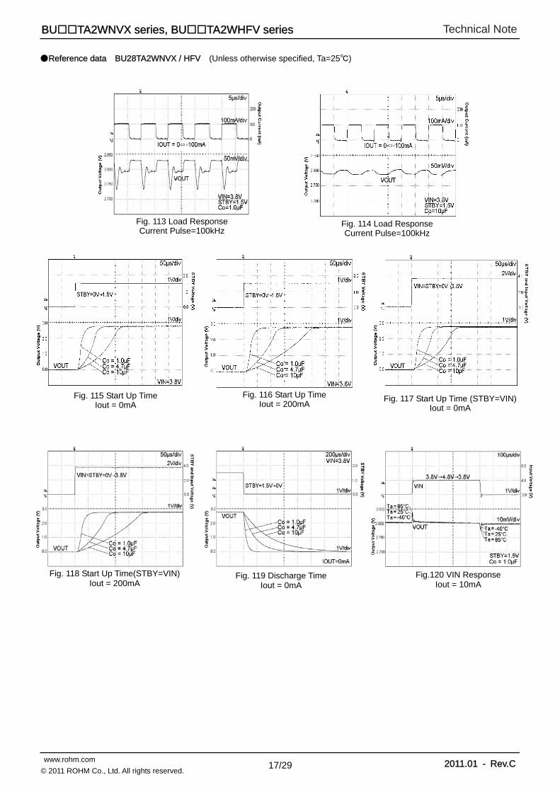
Fig. 113 Load Response Current Pulse=100kHz
Fig. 114 Load Response Current Pulse=100kHz
Fig. 115 Start Up Time Iout = 0mA
Fig. 116 Start Up TimeIout = 200mA
Fig. 117 Start Up Time (STBY=VIN)Iout = 0mA
Fig. 119 Discharge Time Iout = 0mA
Fig.120 VIN Response Iout = 10mA
Fig. 118 Start Up Time(STBY=VIN) Iout = 200mA
⇔
⇔
Technical Note
18/29
BUTA2WNVX series, BUTA2WHFV series
www.rohm.com 2011.01 - Rev.C© 2011 ROHM Co., Ltd. All rights reserved.
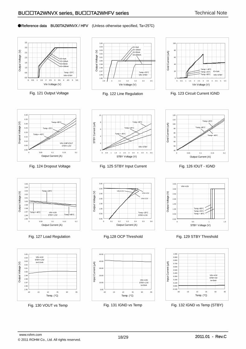
Fig. 121 Output Voltage Fig. 122 Line Regulation
Fig. 130 VOUT vs Temp
Reference data BU30TA2WNVX / HFV (Unless otherwise specified, Ta=25)
Fig. 123 Circuit Current IGND
Fig. 125 STBY Input Current Fig. 126 IOUT - IGND
Fig. 132 IGND vs Temp (STBY) Fig. 131 IGND vs Temp
Fig. 127 Load Regulation Fig. 129 STBY Threshold Fig.128 OCP Threshold
Fig. 124 Dropout Voltage
0.0
0.5
1.0
1.5
2.0
2.5
3.0
3.5
0 0.5 1 1.5 2 2.5 3 3.5 4 4.5 5 5.5
Vin Voltage (V)
Out
put V
olta
ge (
V)
Temp.=25°C
IO=0uAIO=100uAIO=50mAIO=200mA
VIN=STBY
2.95
2.96
2.97
2.98
2.99
3.00
3.01
3.02
3.03
3.04
3.05
2.9 3 3.1 3.2 3.3 3.4 3.5
Vin Voltage (V)
Out
put V
olta
ge (
V)
Temp.=25°C
IO=0uAIO=100uAIO=50mAIO=200mA
VIN=STBY
0
20
40
60
80
100
0 0.5 1 1.5 2 2.5 3 3.5 4 4.5 5 5.5
Vin Voltage (V)
Gnd
Cur
rent
(uA
)
IO=0uATemp.=-40°CTemp.=25°CTemp.=85°C VIN=STBY
0.00
0.05
0.10
0.15
0.20
0.25
0.30
0.35
0.40
0 0.05 0.1 0.15 0.2
Output Current (A)
Dro
pout
Vol
tage
(V
)
VIN=0.98*VOUTSTBY=1.5V
Temp.=-40°C
Temp.=25°C
Temp.=85°C
0
2
4
6
8
10
0 0.5 1 1.5 2 2.5 3 3.5 4 4.5 5 5.5
STBY Voltage (V)
ST
BY
Cur
rent
(uA
) Temp.=85°C
Temp.=25°C
Temp.=-40°C
VIN=STBY
40
50
60
70
80
90
100
110
120
0 0.05 0.1 0.15 0.2
Output Current (A)
Gnd
Cur
rent
(uA
)
Temp.=85°C
Temp.=25°C
Temp=-40°C
2.95
2.96
2.97
2.98
2.99
3.00
3.01
3.02
3.03
3.04
3.05
0 0.05 0.1 0.15 0.2
Output Current (A)
Out
put V
olta
ge (
V)
VIN=4.0VSTBY=1.5V
Temp.=-40°C
Temp.=25°C
Temp.=85°C
0.00
0.50
1.00
1.50
2.00
2.50
3.00
3.50
0 0.1 0.2 0.3 0.4 0.5 0.6
Output Current (A)
Out
put V
olta
ge (
V) VIN=5.5V
VIN=4.0V
VIN=3.5V
Temp.=25°CSTBY=1.5V
0.00
0.50
1.00
1.50
2.00
2.50
3.00
3.50
0 0.5 1 1.5
STBY Voltage (V)
Out
put V
olta
ge (
V)
VIN=4.0V
Temp.=85°CTemp.=25°CTemp.=-40°C
2.95
2.96
2.97
2.98
2.99
3.00
3.01
3.02
3.03
3.04
3.05
-40 -15 10 35 60 85
Temp. (°C)
Out
put V
olta
ge (
V)
VIN=4.0VSTBY=1.5VIo=0.1mA
0.00
10.00
20.00
30.00
40.00
50.00
-40 -15 10 35 60 85
Temp. (°C)
Inpu
t Cur
rent
(µA
)
VIN=4.0VSTBY=1.5V
Io=0mA
-0.100
0.000
0.100
0.200
0.300
0.400
0.500
0.600
0.700
0.800
0.900
1.000
-40 -15 10 35 60 85
Temp. (°C)
Inpu
t Cur
rent
(µA
)
VIN=4.0VSTBY=0VIo=0mA
Technical Note
19/29
BUTA2WNVX series, BUTA2WHFV series
www.rohm.com 2011.01 - Rev.C© 2011 ROHM Co., Ltd. All rights reserved.
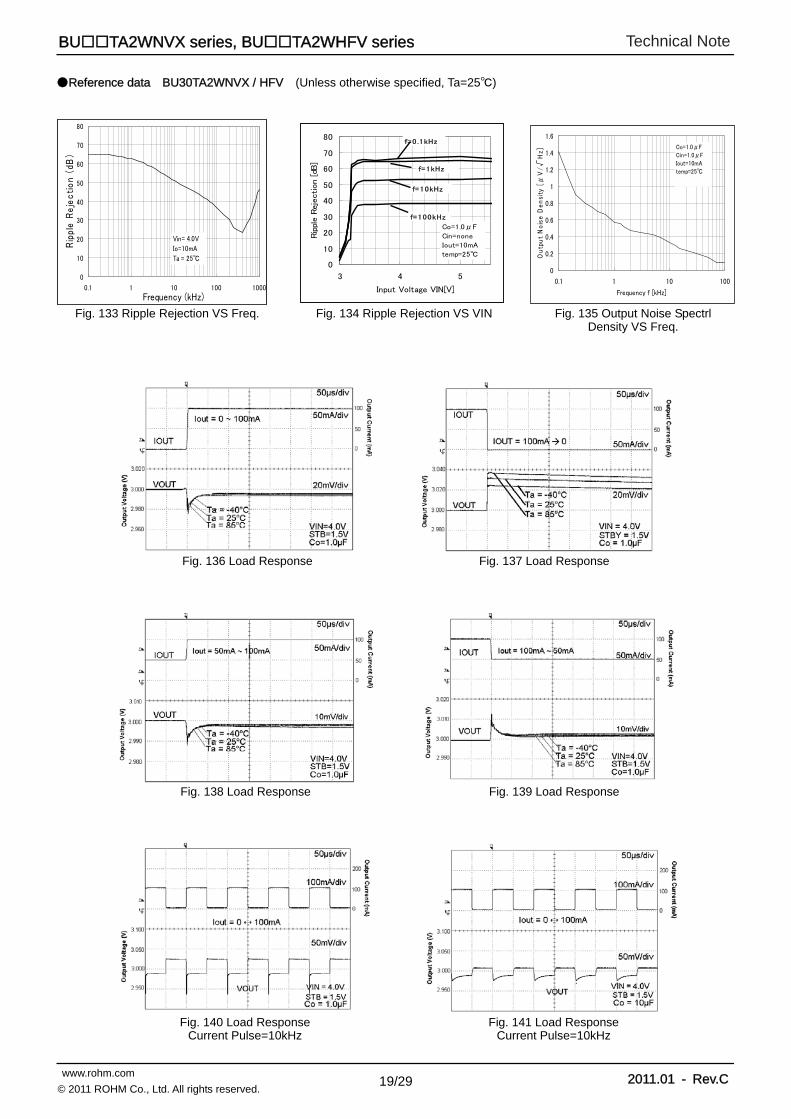
Fig. 133 Ripple Rejection VS Freq. Fig. 134 Ripple Rejection VS VIN Fig. 135 Output Noise SpectrlDensity VS Freq.
Reference data BU30TA2WNVX / HFV (Unless otherwise specified, Ta=25)
Fig. 136 Load Response
Fig. 138 Load Response Fig. 139 Load Response
Fig. 137 Load Response
Fig. 140 Load Response Current Pulse=10kHz
Fig. 141 Load Response Current Pulse=10kHz
0
10
20
30
40
50
60
70
80
0.1 1 10 100 1000
Frequency (kHz)
Rip
ple
Re
jec
tio
n (
dB)
Vin= 4.0V
Io=10mA
Ta = 250
10
20
30
40
50
60
70
80
3 4 5
Input Voltage VIN[V]
Rip
ple R
eje
ction [dB
]
f= 1 00kHz
f=10kHz
f=1kHz
f=0 .1 kHz
Co=1.0μF
Cin=none
Iout=10mA
temp=25
0
0.2
0.4
0.6
0.8
1
1.2
1.4
1.6
0.1 1 10 100
Frequency f [kHz]
Ou
tpu
t N
ois
e D
en
sity
[μ
V/
√H
z]
Co=1.0μFCin=1.0μFIout=10mAtemp=25
Technical Note
20/29
BUTA2WNVX series, BUTA2WHFV series
www.rohm.com 2011.01 - Rev.C© 2011 ROHM Co., Ltd. All rights reserved.
Reference data BU30TA2WNVX / HFV (Unless otherwise specified, Ta=25)
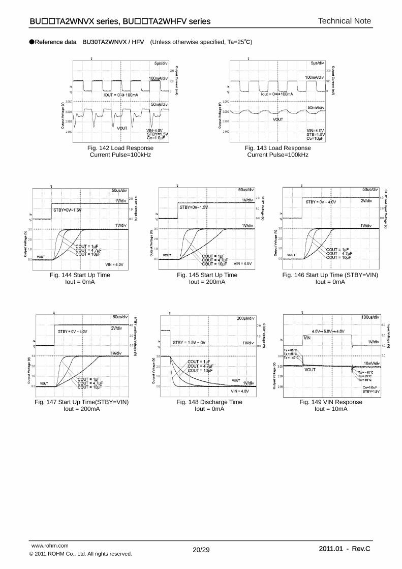
Fig. 142 Load Response Current Pulse=100kHz
Fig. 143 Load Response Current Pulse=100kHz
Fig. 144 Start Up Time Iout = 0mA
Fig. 145 Start Up TimeIout = 200mA
Fig. 146 Start Up Time (STBY=VIN)Iout = 0mA
Fig. 148 Discharge TimeIout = 0mA
Fig. 149 VIN ResponseIout = 10mA
Fig. 147 Start Up Time(STBY=VIN) Iout = 200mA
Technical Note
21/29
BUTA2WNVX series, BUTA2WHFV series
www.rohm.com 2011.01 - Rev.C© 2011 ROHM Co., Ltd. All rights reserved.
Fig. 150 Output Voltage Fig. 151 Line Regulation
Fig. 159 VOUT vs Temp
Reference data BU33TA2WNVX / HFV (Unless otherwise specified, Ta=25)
Fig. 152 Circuit Current IGND
Fig. 154 STBY Input Current Fig. 155 IOUT - IGND
Fig. 161 IGND vs Temp (STBY) Fig. 160 IGND vs Temp
Fig. 156 Load Regulation Fig. 158 STBY Threshold Fig. 157 OCP Threshold
Fig. 153 Dropout Voltage
0.0
0.5
1.0
1.5
2.0
2.5
3.0
3.5
0 0.5 1 1.5 2 2.5 3 3.5 4 4.5 5 5.5
Vin Voltage (V)
Out
put V
olta
ge (
V)
IO=0uAIO=100uAIO=50mAIO=200mA
Temp.=25°CVIN = STBY
3.25
3.26
3.27
3.28
3.29
3.30
3.31
3.32
3.33
3.34
3.35
3.2 3.3 3.4 3.5 3.6 3.7
Vin Voltage (V)
Out
put V
olta
ge (
V)
IO=0uAIO=100uAIO=50mAIO=200mA
Temp=25°CVIN = STBY
0
20
40
60
80
100
0 0.5 1 1.5 2 2.5 3 3.5 4 4.5 5 5.5
Vin Voltage (V)
Gnd
Cur
rent
(uA
)
Temp.=-40°CTemp.=25°CTemp.=85°C
IO=0uAVIN = STBY
0.00
0.05
0.10
0.15
0.20
0.25
0.30
0.35
0 0.05 0.1 0.15 0.2
Output Current (A)
Dro
pout
Vol
tage
(V
)
VIN=0.98 x VOUTSTBY = 1.5V
Temp.=-40°C
Temp.=25°C
Temp.=85°C
0
2
4
6
8
10
0 0.5 1 1.5 2 2.5 3 3.5 4 4.5 5 5.5
VSTBY Voltage (V)
ST
BY
Cur
rent
(uA
)
VIN = STBY
Temp.=85°C
Temp.=25°C
Temp.=-40°C
40
50
60
70
80
90
100
110
120
0 0.05 0.1 0.15 0.2
Output Current (A)
Gnd
Cur
rent
(uA
)
VIN = 4.3VSTBY = 1.5V
Temp.=85°C
Temp.=25°C
Temp.=-40°C
3.25
3.26
3.27
3.28
3.29
3.30
3.31
3.32
3.33
3.34
3.35
0 0.05 0.1 0.15 0.2
Output Current (A)
Out
put V
olta
ge (
V)
VIN = 4.3VSTBY = 1.5V
Temp.=-40°CTemp.=25°C
Temp.=85°C
0.00
0.50
1.00
1.50
2.00
2.50
3.00
3.50
0 0.1 0.2 0.3 0.4 0.5 0.6
Output Current (A)
Out
put V
olta
ge (
V) VIN=5.5V
STBY = 1.5V
Temp=25
VIN=4.3V
VIN=3.8V
0.00
0.50
1.00
1.50
2.00
2.50
3.00
3.50
0 0.5 1 1.5
STBY Voltage (V)
Out
put V
olta
ge (
V)
VIN=4.3V
Temp.=85°CTemp.=25°CTemp.=-40°C
3.25
3.26
3.27
3.28
3.29
3.30
3.31
3.32
3.33
3.34
3.35
-40 -15 10 35 60 85
Temp. (°C)
Out
put V
olta
ge (
V)
VIN=4.3VSTBY=1.5VIo=0.1mA
0.00
10.00
20.00
30.00
40.00
50.00
-40 -15 10 35 60 85
Temp. (°C)
Gnd
Cur
rent
(uA
)
VIN=4.3V
STBY=1.5VIo=0mA
-0.100
0.000
0.100
0.200
0.300
0.400
0.500
0.600
0.700
0.800
0.900
1.000
-40 -15 10 35 60 85
Temp. (°C)
Gnd
Cur
rent
(uA
)
VIN=4.3VSTBY=0V
Technical Note
22/29
BUTA2WNVX series, BUTA2WHFV series
www.rohm.com 2011.01 - Rev.C© 2011 ROHM Co., Ltd. All rights reserved.
Fig. 162 Ripple Rejection VS Freq. Fig. 163 Ripple Rejection VS VIN Fig. 164 Output Noise Spectrl Density VS Freq.
Reference data BU33TA2WNVX / HFV (Unless otherwise specified, Ta=25)
Fig. 165 Load Response
Fig. 167 Load Response Fig. 168 Load Response
Fig. 166 Load Response
Fig. 169 Load Response Current Pulse=10kHz
Fig. 170 Load Response Current Pulse=10kHz
0
0.2
0.4
0.6
0.8
1
1.2
1.4
1.6
1.8
0.1 1 10 100
Frequency f [kHz]
Ou
tpu
t N
ois
e D
en
sity
[μ
V/
√H
z] Co=1.0μFCin=1.0μFIout=10mAtemp=25
0
10
20
30
40
50
60
70
80
3.3 4.3 5.3
Input Voltage VIN[V]
Rip
ple R
eje
cti
on [
dB]
f= 1 00kHz
f=10kHz
f=1kHz
f=0 .1 kHz
Co=1.0μF
Cin=none
Iout=10mA
temp=25
0
10
20
30
40
50
60
70
80
0.1 1 10 100 1000
Frequency (kHz)
Rip
ple
Re
jec
tio
n (
dB)
Vin= 4.3V
Io=10mA
Ta = 25
Technical Note
23/29
BUTA2WNVX series, BUTA2WHFV series
www.rohm.com 2011.01 - Rev.C© 2011 ROHM Co., Ltd. All rights reserved.
Reference data BU33TA2WNVX / HFV (Unless otherwise specified, Ta=25)
Fig. 171 Load Response Current Pulse=100kHz
Fig. 172 Load Response Current Pulse=100kHz
Fig. 173 Start Up Time Iout = 0mA
Fig. 174 Start Up Time Iout = 200mA
Fig. 175 Start Up Time (STBY=VIN)Iout = 0mA
Fig. 177 Discharge Time Iout = 0mA
Fig. 178 VIN Response Iout = 10mA
Fig. 176 Start Up Time(STBY=VIN) Iout = 200mA
Technical Note
24/29
BUTA2WNVX series, BUTA2WHFV series
www.rohm.com 2011.01 - Rev.C© 2011 ROHM Co., Ltd. All rights reserved.
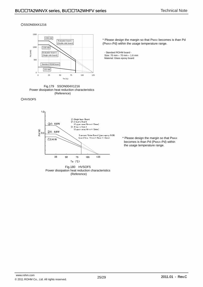
About power dissipation (Pd) As for power dissipation, an approximate estimate of the heat reduction characteristics and internal power consumption of IC are shown, so please use these for reference. Since power dissipation changes substantially depending on the implementation conditions (board size, board thickness, metal wiring rate, number of layers and through holes, etc.), it is recommended to measure Pd on a set board. Exceeding the power dissipation of IC may lead to deterioration of the original IC performance, such as causing operation of the thermal shutdown circuit or reduction in current capability. Therefore, be sure to prepare sufficient margin within power dissipation for usage.
Calculation of the maximum internal power consumption of IC (PMAX) PMAX=(VIN-VOUT)×IOUT(MAX.) (VIN: Input voltage VOUT: Output voltage IOUT(MAX): Maximum output current)
Measurement conditions
Evaluation Board 1 (Single-side Board)
Evaluation Board 2 (Double-side Board)
Layout of Board for Measurement
(Unit: mm)
IC Implementation Position
Top Layer (Top View) Top Layer (Top View)
Bottom Layer (Top View) Bottom Layer (Top View)
Measurement State With board implemented (Wind speed 0 m/s) With board implemented (Wind speed 0 m/s)
Board Material Glass epoxy resin (Single-side board) Glass epoxy resin (Double-side board)
Board Size 40 mm x 40 mm x 0.8 mm 40 mm x 40 mm x 0.8 mm
Wiring Rate Top layer Metal (GND) wiring rate: Approx. 25% Metal (GND) wiring rate: Approx. 25%
Bottom layer Metal (GND) wiring rate: Approx 0% Metal (GND) wiring rate: Approx 25%
Through Hole 0 holes Diameter 0.5 mm 12 holes
Power Dissipation 1100 mW 1250 mW
Thermal Resistance θja=91/W θja=80/W
40
20
40
20
40 40
20
40 20 40 20
40 20 40
Technical Note
25/29
BUTA2WNVX series, BUTA2WHFV series
www.rohm.com 2011.01 - Rev.C© 2011 ROHM Co., Ltd. All rights reserved.
SSON004X1216
HVSOF5
* Please design the margin so that PMAX becomes is than Pd (PMAXPd) within the usage temperature range.
- Standard ROHM board - Size: 70 mm 70 mm 1.6 mm Material: Glass epoxy board
0
500
1000
1500
0 25 50 75 100 125
Ta ()
Pd
(mW
)
Evaluation board 2(Double-side board)
Evaluation board 1(Single-side board)
Standard ROHM board
1250 mW
1100 mW
220 mW
Fig.179 SSON004X1216 Power dissipation heat reduction characteristics
(Reference)
Fig.180 HVSOF5 Power dissipation heat reduction characteristics
(Reference)
* Please design the margin so that PMAX becomes is than Pd (PMAXPd) within the usage temperature range.
P
d(W
)
Technical Note
26/29
BUTA2WNVX series, BUTA2WHFV series
www.rohm.com 2011.01 - Rev.C© 2011 ROHM Co., Ltd. All rights reserved.
DEVICE TYPE & Mark
a
XX output voltage
package
SSON004X1216 HVSOF5
15 1.5V typ. AA BA
18 1.8V typ. AB BB
25 2.5V typ. AC BD
26 2.6V typ. AD BE
27 2.7V typ. AE BF
28 2.8V typ. AF BG
2J 2.85V typ. AG BH
29 2.9V typ. AH BJ
30 3.0V typ. AJ BK
31 3.1V typ. AK BL
32 3.2V typ. AL BM
33 3.3V typ. AM BN
34 3.4V typ. AN BP
Device type: BUXXTA2WNVX
a
Device type: BUXXTA2WHFV
a
SSON004X1216 HVSOF5
Technical Note
27/29
BUTA2WNVX series, BUTA2WHFV series
www.rohm.com 2011.01 - Rev.C© 2011 ROHM Co., Ltd. All rights reserved.
SSON004X1216
HVSOF5
Mark
Lot No.
Mark
Lot No.
Technical Note
28/29
BUTA2WNVX series, BUTA2WHFV series
www.rohm.com 2011.01 - Rev.C© 2011 ROHM Co., Ltd. All rights reserved.
Notes for use
・About absolute maximum rating Breakage may occur when absolute maximum ratings such as applied voltage and operating temperature range are exceeded. Short mode or open mode cannot be specified at occurrence of a break, so please prepare physical safety measures (e.g., fuse) if such special mode in which the absolute maximum rating is exceeded can be assumed.
・About GND potential Please be sure that the potential of the GND terminal is the lowest in any operating condition.
・About thermal design Please provide thermal design with sufficient margin, taking power dissipation (Pd) in actual usage conditions into consideration.
・About short between pins and misattachment Please be careful regarding the IC direction and misalignment at attachment onto a printed circuit board. Misattachment may cause a break of IC. Short caused by foreign matter between outputs, output and power supply, or GNDs may also lead to a break.
・About operation in a strong electromagnetic field Please note that usage in a strong electromagnetic field may cause malfunction.
・About common impedance Please give due consideration to wiring of the power source and GND by reducing common-mode ripple or making ripple as small as possible (e.g., making the wiring as thick and short as possible, or reducing ripple by LC), etc.
・About STBY terminal voltage Set STBY terminal voltage to 0.3 V or less to put each channel into a standby state and to 1.5 V or more to put each channel into an operating state. Do not fix STBY terminal voltage to 0.3 V or more and 1.5 V or less or do not lengthen the transition time. This may cause malfunction or failure. When shorting the VIN terminal and STBY terminal for usage, the status will be “STBY=VIN=LOW” at turning the power OFF, and discharge of the VOUT terminal cannot operate, which means voltage may remain for a certain time in the VOUT terminal. Since turning the power ON again in this state may cause overshoot, turn the power ON for use after the VOUT terminal is completely discharged.
・About overcurrent protection circuit Output has a built-in overcurrent protection circuit, which prevents IC break at load short. Note that this protection circuit is effective for prevention of breaks due to unexpected accidents. Please avoid usage by which the protection circuit operates continuously.
・About thermal shutdown Output is OFF when the thermal circuit operates since a temperature protection circuit is built in to prevent thermal breakdown. However, it recovers when the temperature returns to a certain temperature. The thermal circuit operates at emergency such as overheating of IC. Since it is prepared to prevent IC breakdown, please do not use it in a state in which protection works.
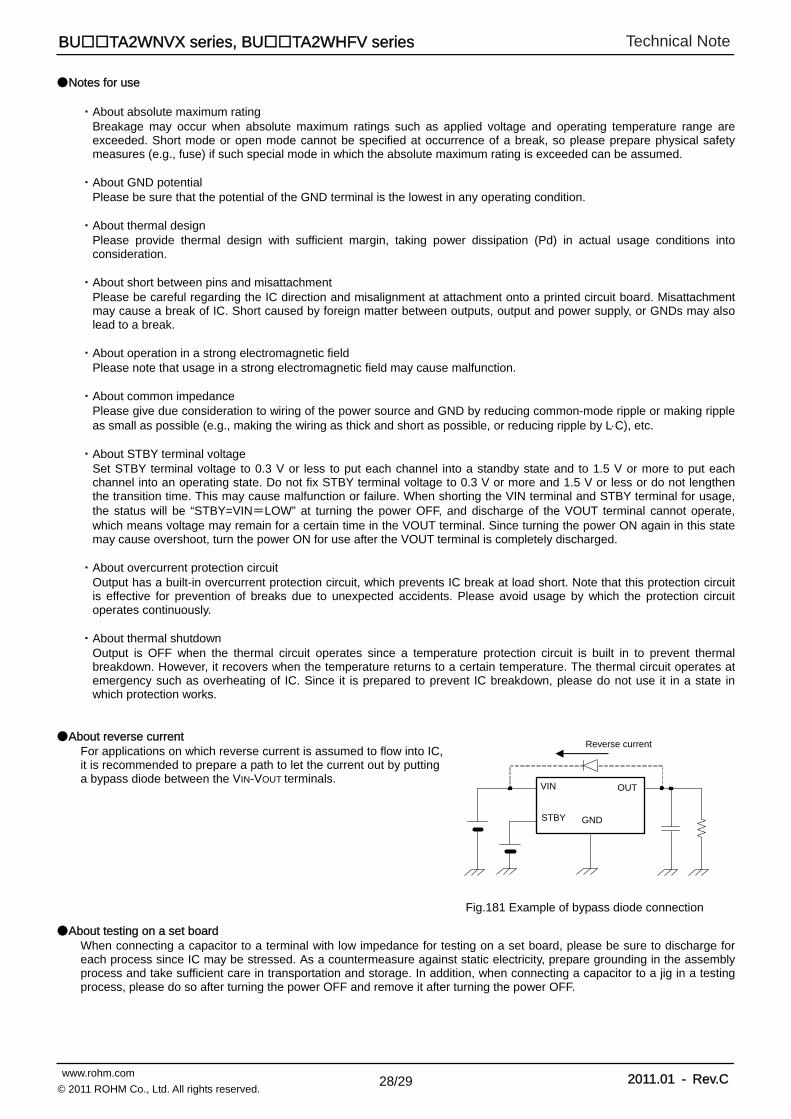
About reverse current For applications on which reverse current is assumed to flow into IC, it is recommended to prepare a path to let the current out by putting a bypass diode between the VIN-VOUT terminals.
About testing on a set board When connecting a capacitor to a terminal with low impedance for testing on a set board, please be sure to discharge for each process since IC may be stressed. As a countermeasure against static electricity, prepare grounding in the assembly process and take sufficient care in transportation and storage. In addition, when connecting a capacitor to a jig in a testing process, please do so after turning the power OFF and remove it after turning the power OFF.
Fig.181 Example of bypass diode connection
Reverse current
VIN
GND STBY
OUT
Technical Note
29/29
BUTA2WNVX series, BUTA2WHFV series
www.rohm.com 2011.01 - Rev.C© 2011 ROHM Co., Ltd. All rights reserved.
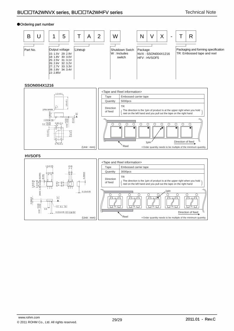
Ordering part number
B U 1 5 T A 2 W N V X - T R
Part No. Output voltage Lineup Shutdown SwichW : Includes switch
Package NVX : SSON004X1216 HFV : HVSOF5
Packaging and forming specificationTR: Embossed tape and reel 15: 1.5V
18: 1.8V 25: 2.5V 26: 2.6V 27: 2.7V 28: 2.8V 2J: 2.85V
29: 2.9V30: 3.0V31: 3.1V32: 3.2V33: 3.3V34: 3.4V
(Unit : mm)
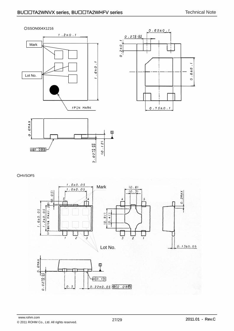
SSON004X1216
S
0.08 S
34
21
1PIN MARK
1.2±0.1
0.65±0.1
0.75±0.1
1.6
±0.1
0.2
±0.1
0.8
±0.1
0.6M
AX
(0.1
2)
0.02
+0.
03-0
.02
0.2+0.05-0.04
∗ Order quantity needs to be multiple of the minimum quantity.
<Tape and Reel information>
Embossed carrier tapeTape
Quantity
Direction of feed The direction is the 1pin of product is at the upper right when you hold
reel on the left hand and you pull out the tape on the right hand
5000pcs
TR
( )
Direction of feed
Reel1pin
(Unit : mm)
HVSOF5
S
0.08 M
0.1 S
4
321
5
(0.0
5)
1.6±0.05
1.0±0.05
1.6±
0.05
1.2±
0.05
(MA
X 1
.28
incl
ude
BU
RR
)
4 5
3 2 1
(0.8)
(0.9
1)
(0.3)
(0.4
1)
0.2M
AX
0.13±0.05
0.22±0.05
0.6M
AX
0.5
0.02
+0.
03–0
.02
Direction of feed
Reel ∗ Order quantity needs to be multiple of the minimum quantity.
<Tape and Reel information>
Embossed carrier tapeTape
Quantity
Direction of feed
The direction is the 1pin of product is at the upper right when you hold reel on the left hand and you pull out the tape on the right hand
3000pcs
TR
( )1pin
DatasheetDatasheet
Notice - GE Rev.002© 2014 ROHM Co., Ltd. All rights reserved.
Notice Precaution on using ROHM Products
1. Our Products are designed and manufactured for application in ordinary electronic equipments (such as AV equipment, OA equipment, telecommunication equipment, home electronic appliances, amusement equipment, etc.). If you intend to use our Products in devices requiring extremely high reliability (such as medical equipment (Note 1), transport equipment, traffic equipment, aircraft/spacecraft, nuclear power controllers, fuel controllers, car equipment including car accessories, safety devices, etc.) and whose malfunction or failure may cause loss of human life, bodily injury or serious damage to property (“Specific Applications”), please consult with the ROHM sales representative in advance. Unless otherwise agreed in writing by ROHM in advance, ROHM shall not be in any way responsible or liable for any damages, expenses or losses incurred by you or third parties arising from the use of any ROHM’s Products for Specific Applications.
(Note1) Medical Equipment Classification of the Specific Applications JAPAN USA EU CHINA
CLASSⅢ CLASSⅢ
CLASSⅡb CLASSⅢ
CLASSⅣ CLASSⅢ
2. ROHM designs and manufactures its Products subject to strict quality control system. However, semiconductor
products can fail or malfunction at a certain rate. Please be sure to implement, at your own responsibilities, adequate safety measures including but not limited to fail-safe design against the physical injury, damage to any property, which a failure or malfunction of our Products may cause. The following are examples of safety measures:
[a] Installation of protection circuits or other protective devices to improve system safety [b] Installation of redundant circuits to reduce the impact of single or multiple circuit failure
3. Our Products are designed and manufactured for use under standard conditions and not under any special or extraordinary environments or conditions, as exemplified below. Accordingly, ROHM shall not be in any way responsible or liable for any damages, expenses or losses arising from the use of any ROHM’s Products under any special or extraordinary environments or conditions. If you intend to use our Products under any special or extraordinary environments or conditions (as exemplified below), your independent verification and confirmation of product performance, reliability, etc, prior to use, must be necessary:
[a] Use of our Products in any types of liquid, including water, oils, chemicals, and organic solvents [b] Use of our Products outdoors or in places where the Products are exposed to direct sunlight or dust [c] Use of our Products in places where the Products are exposed to sea wind or corrosive gases, including Cl2,
H2S, NH3, SO2, and NO2
[d] Use of our Products in places where the Products are exposed to static electricity or electromagnetic waves [e] Use of our Products in proximity to heat-producing components, plastic cords, or other flammable items [f] Sealing or coating our Products with resin or other coating materials [g] Use of our Products without cleaning residue of flux (even if you use no-clean type fluxes, cleaning residue of
flux is recommended); or Washing our Products by using water or water-soluble cleaning agents for cleaning residue after soldering
[h] Use of the Products in places subject to dew condensation
4. The Products are not subject to radiation-proof design. 5. Please verify and confirm characteristics of the final or mounted products in using the Products. 6. In particular, if a transient load (a large amount of load applied in a short period of time, such as pulse. is applied,
confirmation of performance characteristics after on-board mounting is strongly recommended. Avoid applying power exceeding normal rated power; exceeding the power rating under steady-state loading condition may negatively affect product performance and reliability.
7. De-rate Power Dissipation (Pd) depending on Ambient temperature (Ta). When used in sealed area, confirm the actual
ambient temperature. 8. Confirm that operation temperature is within the specified range described in the product specification. 9. ROHM shall not be in any way responsible or liable for failure induced under deviant condition from what is defined in
this document.
Precaution for Mounting / Circuit board design 1. When a highly active halogenous (chlorine, bromine, etc.) flux is used, the residue of flux may negatively affect product
performance and reliability. 2. In principle, the reflow soldering method must be used; if flow soldering method is preferred, please consult with the
ROHM representative in advance. For details, please refer to ROHM Mounting specification
DatasheetDatasheet
Notice - GE Rev.002© 2014 ROHM Co., Ltd. All rights reserved.
Precautions Regarding Application Examples and External Circuits 1. If change is made to the constant of an external circuit, please allow a sufficient margin considering variations of the
characteristics of the Products and external components, including transient characteristics, as well as static characteristics.
2. You agree that application notes, reference designs, and associated data and information contained in this document
are presented only as guidance for Products use. Therefore, in case you use such information, you are solely responsible for it and you must exercise your own independent verification and judgment in the use of such information contained in this document. ROHM shall not be in any way responsible or liable for any damages, expenses or losses incurred by you or third parties arising from the use of such information.
Precaution for Electrostatic
This Product is electrostatic sensitive product, which may be damaged due to electrostatic discharge. Please take proper caution in your manufacturing process and storage so that voltage exceeding the Products maximum rating will not be applied to Products. Please take special care under dry condition (e.g. Grounding of human body / equipment / solder iron, isolation from charged objects, setting of Ionizer, friction prevention and temperature / humidity control).
Precaution for Storage / Transportation 1. Product performance and soldered connections may deteriorate if the Products are stored in the places where:
[a] the Products are exposed to sea winds or corrosive gases, including Cl2, H2S, NH3, SO2, and NO2 [b] the temperature or humidity exceeds those recommended by ROHM [c] the Products are exposed to direct sunshine or condensation [d] the Products are exposed to high Electrostatic
2. Even under ROHM recommended storage condition, solderability of products out of recommended storage time period may be degraded. It is strongly recommended to confirm solderability before using Products of which storage time is exceeding the recommended storage time period.
3. Store / transport cartons in the correct direction, which is indicated on a carton with a symbol. Otherwise bent leads
may occur due to excessive stress applied when dropping of a carton. 4. Use Products within the specified time after opening a humidity barrier bag. Baking is required before using Products of
which storage time is exceeding the recommended storage time period.
Precaution for Product Label QR code printed on ROHM Products label is for ROHM’s internal use only.
Precaution for Disposition When disposing Products please dispose them properly using an authorized industry waste company.
Precaution for Foreign Exchange and Foreign Trade act Since our Products might fall under controlled goods prescribed by the applicable foreign exchange and foreign trade act, please consult with ROHM representative in case of export.
Precaution Regarding Intellectual Property Rights 1. All information and data including but not limited to application example contained in this document is for reference
only. ROHM does not warrant that foregoing information or data will not infringe any intellectual property rights or any other rights of any third party regarding such information or data. ROHM shall not be in any way responsible or liable for infringement of any intellectual property rights or other damages arising from use of such information or data.:
2. No license, expressly or implied, is granted hereby under any intellectual property rights or other rights of ROHM or any
third parties with respect to the information contained in this document.
Other Precaution 1. This document may not be reprinted or reproduced, in whole or in part, without prior written consent of ROHM. 2. The Products may not be disassembled, converted, modified, reproduced or otherwise changed without prior written
consent of ROHM. 3. In no event shall you use in any way whatsoever the Products and the related technical information contained in the
Products or this document for any military purposes, including but not limited to, the development of mass-destruction weapons.
4. The proper names of companies or products described in this document are trademarks or registered trademarks of
ROHM, its affiliated companies or third parties.
DatasheetDatasheet
Notice – WE Rev.001© 2014 ROHM Co., Ltd. All rights reserved.
General Precaution 1. Before you use our Pro ducts, you are requested to care fully read this document and fully understand its contents.
ROHM shall n ot be in an y way responsible or liabl e for fa ilure, malfunction or acci dent arising from the use of a ny ROHM’s Products against warning, caution or note contained in this document.
2. All information contained in this docume nt is current as of the issuing date and subj ect to change without any prior
notice. Before purchasing or using ROHM’s Products, please confirm the la test information with a ROHM sale s representative.
3. The information contained in this doc ument is provi ded on an “as is” basis and ROHM does not warrant that all
information contained in this document is accurate an d/or error-free. ROHM shall not be in an y way responsible or liable for any damages, expenses or losses incurred by you or third parties resulting from inaccuracy or errors of or concerning such information.