Embed Size (px)
Citation preview
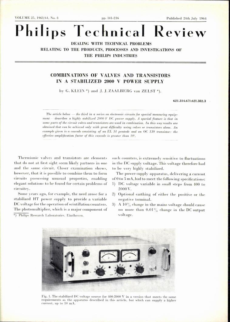
VOLUME 25, 1963/64, No. 8 pp. 181-216 Published 24th July 1964
Philips Technical ReviewDEALING WITH TECHNICAL PROBLEMS
RELATING TO THE PRODUCTS, PROCESSES AND INVESTIGATIONS OFTHE PHILIPS INDUSTRIES
COMBINATIONS OF VALVES AND TRANSISTORSIN A STABILIZED 2000 V POWER SUPPLY
by G. KLEIN *) and J. J. ZAALBERG van ZELST *).
621.314.671:621.382.3 .
The article below - the third in a series on electronic circuits for special measuring equip-ment - describes a highly stabilized 2000 V DC power supply. A special feature is that insome parts of the circuit valves and tr an.sistors are used in com.bination. In this way results areobtained that can be achieved only with great difficulty using valves or transistors alone. Anexample given is a cascade consisting of an EL 34 pentode and an OC 139 transistor: the~ffective omplificoiiorc factor of this cascode is greater than 105•
Thermionic valves and transistors are elementsthat do not at first sight seem likely partners in oneand the same circuit. Closer examination shows,however, that it is possible to combine them to formcircuits possessing unusual properties, enablingelegant solutions to be found for certain problems ofcircuitry.
Some years ago, for example, the need arose for astabilized HT power supply to provide a variableDC voltage for the opera tion of scintillation counters.The photomultiplier, which is a major component of*) Philips Research Labora tories , Eindhoven.
such counters, is ext.rernelv sensitive to fluctuationsin the DC supply voltage. This voltage therefore hadto be very highly stabilized.The power-supply apparatus, delivering a current
of 0 to 5 mA, had to meet the following specifications:1) DC voltage variable in small steps from 400 to
2000V.2) Optional earthing of either the positive or the
negative terminal.3) A 10% change in the mains voltage should cause
no more than 0.01 % change in the DC outputvoltage.
Fig. 1. The stabilized DC voltage source for 400-2000 V in a version that meets the samerequirements as the apparatus described in this article, hut which can supply a highercurrent, up to 10 mA.
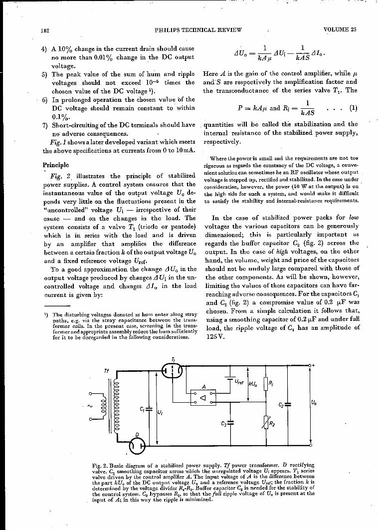
182 PHILlPS TECHNICAL REVIEW VOLUME 25
4.) A 10% change in the current drain should causeno more than 0.01% change in the DC outputvoltage.
S) The peak value of the sum of hlim and ripplevoltages should not exceed 10-5 times thechosen value of the DC voltage 1).
6) In prolonged operation the chosen value of theDC voltage should remain constant to' within0.1%.
7) Short-circuiting of the DC terminals should haveno adverse consequences.Fig.1 shows a later developed variant which meets
the above specifications at currents from 0 to 10mA.
Principle.Fig. 2, illustrates the principle of stabilized
power supplies. A control system ensures that theinstantaneous value of the output voltage U0 de-pends very little on the fluctuations present in the"uncontrolled" voltage Ui - irrespective of theircause - and on the changes in the load. Thesystem consists of a valve Tl (triode or pentode)which is in series with the load and is drivenby an amplifier that amplifies the differencebetween a certain fraction k ofthe output voltage Uoand a fixed reference voltage Uref.To a good approximation the change .1Uo in the
output voltage produced by changes .1 Ui in the un-controlled voltage and changes .110 in the loadcurrent is given by:
1) The disturbing voltages denoted as hum enter along straypaths, e.g, via the stray capacitance between the trans-former coils. In the present case, screening in the trans-former and appropriate assembly reducethe hum sufficientlyfor it to be disregarded in the followingconsiderations.
1 1L1Uo = -- L1Ui --SLl1o.kAp, kA
Here A is the gain of the control amplifier, while Itand'S are respectively the amplification factor andthe transconductance of the series valve Tl' The
1P = kAlt and R; = --
kAS(1)
, quantities will he called the stabilization and theinternal resistance of the stabilized power supply,respectivel y.
Where the power is small and the requirements are not toorigorous as regards the constancy of the DC voltage, a conve-nientsolutioncan sometimes be an RF oscillator whose outputvoltage is stepped up, rectified and stabilized. In the case underconsideration, however, the power (10 \.Vat the output) is onthe high side for such a system, and would make it difficultto satisfy the stability and internal-resistance requirements.
In the case of stabilized power packs for lowvoltages the various capacitors can be generouslydimensioned; this is particularly important asregards the buffer capacitor C2 (fig. 2) across theoutput. In the case of high voltages, on the otherhand, the volume, weight and price of the capacitorsshould not be unduly large compared with those ofthe other components. As will be shown, however,limiting the values of these capacitors can have far-reaching adverse consequences. For the capacitors Cland C2 (fig. 2) a compromise value of 0.2 fLF waschosen. From a simple calculation it follows that,using a smoothing capacitor of 0.2 fLFand under fullload, the ripple voltage of Cl has an amplitude of12SV.
JFig. 2. Basic diagram of a stabilized power supply. Tf power transformer. D rectifyingvalve. Cl smoothing capacitor acrosswhich the unregulated voltage Ui appears. Tl seriesvalve driven by the control amplifierA. The input voltage of A is the differencebetweenthe part kUo of the DC output voltage Uo and a reference voltage Uref; the fraction k isdetermined by the voltage divider RCR2' Buffer capacitor C2 is needed for the stability ofthe control system. C3 bypasses R2' so that the full ripple voltage of Uo is present at theinput of A; in this way the ripple is minimized.
1963/64.. No. 8 A STABILIZED 2000 V POWER SUPPLY 183
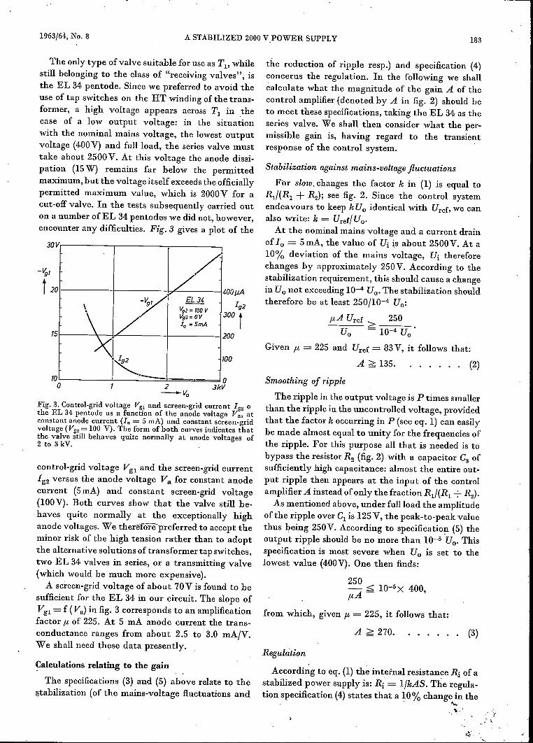
The only type of valve suitable for use as Tl' whilestill belonging to the class of "receiving valves", isthe EL 34,pentode. Since we preferred to avoid theuse of tap switches on the HT winding of the trans-former, a high voltage appears across TJ in thecase of a low output voltage: in the situationwith the nominal mains voltage, the lowest outputvoltage (400V) and fullload, the series valve musttake about 2500V. At this voltage the anode dissi-pation (15W) remains far below the permittedmaximum, but the voltage itself exceeds the officiallypermitted maximum v:alue, which is 2000V for acut-off valve. In the tests subsequently carried outon a number of EL 34 pentodes we did not, however,encounter any difficulties. Fig.3 gives a plot of the
3oVr---------.---------~------~
-Vg,
t 20~--------~--------~~----~~0~A)Vgl• EL34 I
Vg2= lOO V g2• Vg3=OV 300t
Ia = 5mAf5~----+--!.£_--------_I___------~ 200
Ix 192~x __ x_
fO'------- L- ---========oI 0o 2 JW
---VaFig. ;j. Control-gridvoltage Vg1 and screen-grid current Ig2 0
the EL 34 pentode as a function of the anode voltage Va. atconstant anode current (In = 5 mA) and constant screen-gridvoltage (Vg2 = 100 V). The form of both curves indicates thatthe valve still behaves quite normally at anode voltages of2 to 3 kV.
too
control-grid voltage Vgl and the screen-grid currentIg2 versus the anode voltage Va for constant anodecurrent (5mA) and constant screen-grid voltage(IOOV). Both curves show that the valve still be-haves quite normally at the exceptionally highanode voltages. We therëfórê preferred to accept theminor risk of the high tension rather than to adoptthe alternative solutions of transformer tap switches,two EL 34 valves in series, or a transmitting valve(which would be much more expensive).A screen-grid voltage of about 70V is found to be
sufficient for the EL 34. in our circuit. The slope ofVgl = f (Va) in fig. 3 corresponds to an amplificationfactor I-t of 225. At 5 mA anode current the trans-conductance ranges from about 2.5 to 3.0 mA/V.We shall need these data presently.
Calculations relating to the gain
The specifications (3) and (5) above relate to thestabilization (of the mains-voltage fluctuations and
the reduction of ripple resp.) and specification (4,)concerns the regulation. In the following we shallcalculate what the magnitude of the gain A of thecontrol amplifier (denoted by A in fig. 2) should beto meet these specifications, taking the EL 34 as theseries valve. We shall then consider what the per-missible gain is, having regard to the transientresponse of the control system.
Stabilization against mains-voltage fluctuations
For slow. changes the factor k in (1) is equal toRI/(RI + R2); see fig. 2. Since the control systemendeavours to keep kUo identical with Uref, we canalso write: k = Urer/Uo.At the nominal mains voltage and a current drain
of 10 = 5mA, the value of Ui is about 2500V. At a10% deviation of the mains voltage, Ui thereforechanges by approximately 250V. According to thestabilization requirement, this should cause a changein Uo not exceeding 10-4 Uo• The stabilization shouldtherefore be at least 250/10-4 Uo:
I-tA Uref > 250Uo - 10-4 U;
Given I-t = 225 and Uref = 83V, it follows that:
A ~ 135. (2)
Smoothing of ripple
The ripple in the output voltage is P times smallerthan the ripple in the uncontrolled voltage, providedthat the factor k occurring in P (see eq. 1) can easilybe made almost equal to unity for the frequencies ofthe ripple. For this purpose all that is needed is tobypass the resistor R2 (fig. 2) with a capacitor C3 ofsufficiently high capacitance: almost the entire out-put ripple then appears at the input of the controlamplifier A instead of only the fraction RI/(RI + R2).
As mentioned above, under fullload the amplitudeof the ripple over Cl is 125V, the peak-to-peak valuethus being 250V. According to specification (5) theoutput ripple should be no more than 10-5 Uo. Thisspecification is most severe when U0 is set to thelowest value (4,00V). One then finds:
250- :s;; IO-5X 4,00,I-tA
from which, given f.l = 225, it follows that:
A ~ 270. (3)
Regulation. .
According to eq. (1) the internal resistance R; of astabilized power supply is: R; = I/kAS. The regula-tion specification (4) states that a 10% change in the
... • 11''''",. .
184 PHILIPS TECHNICAL REVIEW VOLUME 25
current 10 should cause a change of no more than10-4 Uo in the output voltage. Hence:
1 10-4 u;-~ .kAS - 0.110
In this expression the maximum value (5mA) shouldbe substituted for 10 and the minimum value(2.5mA/V) for S. We then find, with k = Urer/Uoand Uref = 83V:
A ~ approx. 25.
From (2), (3) and (4.) it follows that all threespecifications are only met where A = 270.
Transient response
Control systems can respond to a step-functiondisturbance in various ways. In general, reactionswith an oscillatory character are undesired: in otherwords, the transient response should show littleor no overshoot. H this requirement is fulfilled, thestability of the control system will be assured, evenwith the conventional tolerance in the values of thecomponents. The question is now whether, in thepresent case, a gain A of 270 is compatible with atransient response without overshoot.
For simple linear control systems with two timeconstants, i1 and i2 < i1, it is easily deduced thatthe condition for the required form of the transientresponse is: loop gain kA ;;;;;!i1/i2' hence:
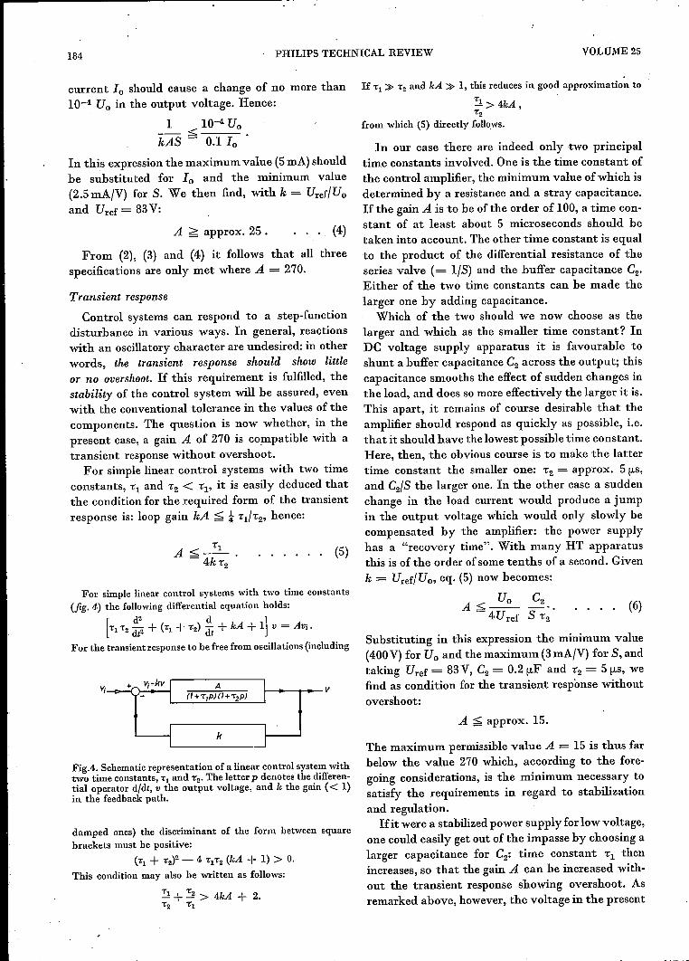
For simple linear control systems with two time constants(fig.4) the following differential equation holds:
[Tl '2 ::2 + (Tl + T2) ~ + kA + 1] v = Av;.
For the transient response to be free from oscillations (including
AVi
k
Fig.4. Schematic representation of a linear control system withtwo time constants, Tl and T2' The letter p denotes the differen-tial operator d/dt, v the output voltage, and k the gain « 1)in the feedback path.
damped ones) the discriminant of the form between squarebrackets must he positive:
(Tl + T2)2 - 4 T1T2 (kA + 1) > O.This condition mayalso he written as follows:
2+~ > 4kA + 2.T2 Tl
If Tl » '2 and kA » 1, this reduces in good approximation to
~>4kA,T2
from which (5) directly follows.
(4)
In our case there are indeed only two principaltime constants involved. One is the time constant ofthe control amplifier, the minimum value of which isdetermined by a resistance and a stray capacitance.Ifthe gain A is to be ofthe order of 100, a time con-stant of at least about 5 microseconds should betaken into account. The other time constant is equalto the product of the differential resistance of theseries valve (= liS) and the buffer capacitance C2•
Either of the two time constants can be made thelarger one by adding capacitance.
Which of the two should we now choose as thelarger and which as the smaller time constant? InDC voltage supply apparatus it is favourable toshunt a buffer capacitance C2 across the output; thiscapacitance smooths the effect of sudden changes inthe load, and does so more effectively the larger it is.This apart, it remains of course desirable that theamplifier should respond as quickly as possible, i.e.that it should have the lowest possible time constant.Here, then, the obvious course is to make the lattertime constant the smaller one: i2 = approx. 5 [LS,
and C2/S the larger one. In the other case a suddenchange in the load current would produce a jumpin the output voltage which would only slowly becompensated by the amplifier: the power supplyhas a "recovery time". With many HT apparatusthis is of the order of some tenths of a second. Givenk = Uref/Uo, eq. (5) now becomes:
c; C2A::;;--- 4Uref S i2
(5)
(6)
Substituting in this expression the minimum value(400V) for U; and the maximum (3mA/V) for S, andtaking Uref = 83V, C2= 0.2 [LF and i2 = 5 [LS, wefind as condition for the transient response withoutovershoot:
A ;;;;;approx. 15.
The maximum permissible value A = 15 is thus farbelow the value 270 which, according to the fore-going considerations, is the minimum necessary tosatisfy the requirements in regard to stabilizationand regulation.
Hit were a stabilized power supply for low voltage,one could easily get out of the impasse by choosing alarger capacitance for C2: time constant i1 thenincreases, so that the gain A can be increased with-out the transient response showing overshoot. Asremarked above, however, the voltage in the present
1963/64,No. 8 A STABILIZED2000V POWER SUPPLY 185
case is so high that C2 should preferably not be largerthan 0.2 [LF.
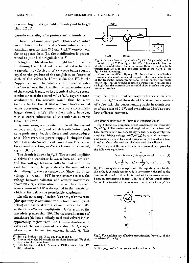
Cascode consisting of a pentode and a transistor
The conflict would disappear if the series valve hadan amplification factor and a transconductance sub-stantially greater than 225 and 3mA/V respectively,for as appears from (1), the stabilization is propor-tional to ft and the regulation to S.
A high amplification factor might be obtained bycombining the EL 34 with a second valve to forma cascode, the effective ft of a cascode being roughlyequal to the product of the amplification factors ofeach of the valves 2). If we make the EL 34. the"upper" valve in the cascode and the second valvethe "lower" one, then the.effective transconductanceof the casco de is more or less identical with the trans-conductance ofthe second valve 2). As regards trans-conductance, the casco de would thus be morefavourable than the EL 34 if one could have a secondvalve possessing a transconductance substantiallylarger than 3 mA/V. No valves exist, however,with a transconductance of this order at currentsfrom 1 to 5 mA.
By now using a transistor in lieu of the secondvalve, a solution is found which is satisfactory bothas regards amplification factor and trans conduct-ance. Moreover, the power supply is simpler thanwith a casco de consisting of two valves. Because ofthe current direction, an N-P-N transistor is needed,e.g. an OC 139.
The circuit is shown infig. 5. The control amplifierA drives the transistor between base and emitter,and the voltage between collector and emitter isused for driving the pentode (for the moment weshall disregard the resistance R3). Since the lattervoltage is -4 and -16V in the extreme cases, thevoltage between collector and emitter never risesabove 20V 3), a value which must not be exceeded.A maximum of 0.1W is dissipated in the transistor,which is far below the permissible maximum.
The effective amplification factor /-ltrof transistors(this quantity is explained in the text in small printbelow) can easily attain a value of more than 500,so that the effective amplification factor /-lcascof thecascode is greater than 105. The transconductance oftransistors (defined similarly to that of valves) is alsoappreciably higher than the transconductance ofvalves at the same current, viz about 40 lemA/V,where le is the emitter current in mA 4). This
2) Seee.g. Philips tech. Rev. 23, 145,1961/62. .3) Exceptwhen the DCterminals are short-circuited.We shall
return to this point later.4) F.H. Stieltjes and L.J. Tummers, Philips tech. Rev. 17,
244, 1955/56.
£L34 OC139
Fig. 5. Cascode formed by a valve Tl (EL 34 pentode) and atransistor Trl (N-P-N type OC139). This cascodehas aneffective amplificationfactor of more than 105 and a hightransconductance; it can therefore replace the valve Tl infig. 2 with advantage.A control amplifier. R3 (e.g, 68 ohms) limits the effective
transconductanceof the cascode(equalto the transconductanceof the transistor, hence proportional to the emitter current);under fullioad the transconductancewould otherwisebecomeso high that the control systemwould show overshootor evenbecomeunstable.
may be put in another way: whereas in valvesthe ratio Ia/Sis of the order of 1V at anode currentsof a few mA, the corresponding ratio in transistorsis of the order of 0.1 V, and even about 25mVat verylow collector currents.
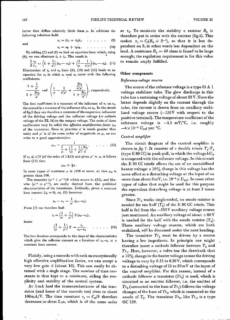
The effective amplification factor of a transistor circuitFig. 6 showsthe simplifiedcircuit contaiuing the transistor
Tri of fig. 5. The resistances through which the emitter andbase currents floware denoted by re and rh respectively,theamplifieddrivingvoltage A(kUo~Urer) by vs, and the currentand voltage changesby i and v respectively; the subscriptse,band c refer to the emitter, the base and the collector. .The changesof the collectorand base currents are givenby
the followingequations:
ie = S(Vh - vc) + .§_ (vc - vc),. (7)ft
ih=~(Vh-VC)-a~,(vc-ve). (8)
Eq. (7) is completelyanalogouswith the equation for a triode,the cathodeofwhichcorrespondsto the emitter, the gridto thebase and the anodeto the collector,andwith a transconductanceS and an amplificationfactor It. In (8) a' is the amplificationfactor ofthe transistorin common-emittercircuits5), and It' is a
Fig.6. For derivingthe effectiveamplificationfactor fltr of thetransistor Tri in fig. 5.
5) See page 242of the article under reference 4).
..----------------------------------------------------------------------------------~------ -
186 PHILIPS TECHNICAL REVIEW VOLUME 25
factor that differs relatively little from It. In addition thefollowing relations hold:
andVs = Vb + ibrb. (10)
By adding (7) and (8) we find an equation from which, using(9), we can eliminate ib + ic. The result is: '
Si~= (1+;) (Vb-Vc) + (~-+,)(vc-vc). (11)rc a ft a It
Elimination of ib and Vb from (8), (10) and (11) leads to anequation for Vc in which Vs and Vc occur with the followingcoefficients: '
_l_+_S"~_ and (!. - -i, + ;:~S' -), respectively.1+ __!.J!. It a It 1+ -'i!--a. a
The first coefficient is a measure of the influence of Vs on Vc,the seeond is a measure of the influence ofVcon vc. In the circuitof fig.5 they are therefore a measure of the respective influencesof the driving voltage and the collector voltage (= cathodevoltage of the EL 34.)on the output voltage. The ratio of thesecoefficients may be called the effective omplification. factor Iltrof the transistor. Since in practice a' is much greater thanunity and 11' is of the same order of magnitude as It, we canwrite to a good approximation:
1. . . . (12)lttr = I ( I I ) s-, .-+ -+,-,
It It It aIf rb ;;;; (l'JS (of the order of 1 kf2) and given It' "'" ft, it followsfrom (12) that
!ltr> tIt.
In most types of transistor ft is 1500 or more, so that Iltr isgreater than 500.The quantity (W1 + !l'-1)S which occurs in (12), and like-
wise (/t-1 + It'-1), are easily derived from the publishedcharacteristics of the transistors. Evidently, given a constantbase ~urr~nt (ib = 0), eq. (8) becomes:
1vb - Vc = -, (vc--ve).
ItFrom (7) we therefore find:
ie = (~+..!,) S (ve-Vc),It It
hence
(1 + 1) S ie,p, It' = vc-Vc' . . . . . (13)
The last fraction corresponds to the slope of the characteristicswhich give the collector current as a function of Vc-Vc at aconstant base current.
Plainly, using a casco de with such an exceptionallyhigh effective amplification factor, we can accept avery low gain A (about 10). This can easily be ob-tained with a single stage. The number of time con-stants is thus kept to a minimum, aiding the sim-plicity and stability of the control system.
At 5mA load the transconductance of the tran-sistor (and hence of the casco de too) rises to about100mA/V. The time constant .1= C2/S thereforedecreases to about 2 [Ls,which is of the same order
(9)
as "2' To maintain the stability a resistor Ra istherefore put in series with the emitter (fig.5). Thismakes "1 = C2(Ra + S-l), so that it is less de-pendent on S, in other words less dependent on theload. A resistance Ra = 68 ohms is found to be largeenough; the regulation requirement is for this valueto remain amply fulfilled.
Other components
Reference-voltage source
The source of the reference voltage is a type 83 A 1voltage stabilizer tube. The glow discharge in thistube has a sustaining voltage of about 83V. Since thelatter depends slightly on the current through thetube, the current is drawn from an auxiliary stabi-lized voltage source (-150V with respect to thepositive terminal). The temperature coefficient ofthereference voltage is -3.5 mVrC, i.e. roughly-4 X 10⁻⁵ Uref per oe.Control amplifier
The circuit diagram of the control amplifier isshown in fig. 7. It consists of a double triode T2-Ta(type E 80 CC) in push-pull, in which the voltagekUois compared with the reference voltage. In this circuitthe E 80 CC triode allows the use of an unstabilizedheater voltage: a 10% change in this voltage has thesame effect as a disturbing voltage at the input of nomore than about 8m V, i.e.l0-4x Uref. In most othertypes of tubes that might be used for this purposethe equivalent disturbing voltage is at least 3 timesgreater.
Since TrI works single-ended, no anode resistor isneeded for one half (T2) of the E 80 CC triode. Thishalf is fed from the -150V auxiliary voltage sourcejust mentioned. An auxiliary voltage of about +80 Vis needed for the half with the anode resistor (Ta)'These auxiliary voltage sources, which are bothstabilized, will be discussed under the next heading.
The transistor TrI must be driven by a sourcehaving a low impedance. In principle one mighttherefore insert a cathode follower between Ta andTrI' Here, however, a valve has the drawback thataIO % change in the heater voltage causes the drivingvoltage to vary by 0.15 to O.20V, which correspondsto a disturbing voltage of 15 to 20mV at the input ofthe control amplifier. For this reason, instead of acathode follower a transistor (Tr2) is used, which iscircuited as an emitter follower, i.e. the emitter ofTr 2 (connected to the base of TrI) follows the voltagechanges of the base of Tr 2' which is connected to theanode of Ta' The transistor Tr2, like TrI' is a typeOe-139.
1963/640, No. 8
~.._~.~---------------..,....,
A STABILIZED 2000V POWER SUPPLY
U.O,2{JF 0
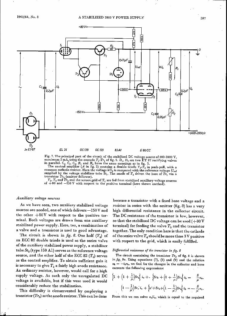
°22xEY87 EL 34 OC139 OC139 83Al E80CC
Fig. 7. The principal part of the circuit of the stabilized DC voltage source of 400-2000V,maximum 5mA,using the cascode Tl-TrI of fig. 5. Dl> D2 are two EY 87 rectifying valvesin parallel. Cl> C2, Ca' RI and R2 have the same meauings as in fig. 2.The control amplifier (A in fig. 2) contains a double triode T2-Ta in push-pull, with a
common cathode resistor. Here the voltage kUo is compared with the reference voltage Urefsupplied by the voltage stabilizer tube Stp The anode of Ta drives the hase of TrI via atransistor Tr2 (emitter follower).
T2, Ta and Tr2 and the screen grid of Tl are fed from stabilized auxiliary voltage sourcesof +80 and -150 V with respect to the positive terminal (here shown earthed).
Auxiliary voltage sources
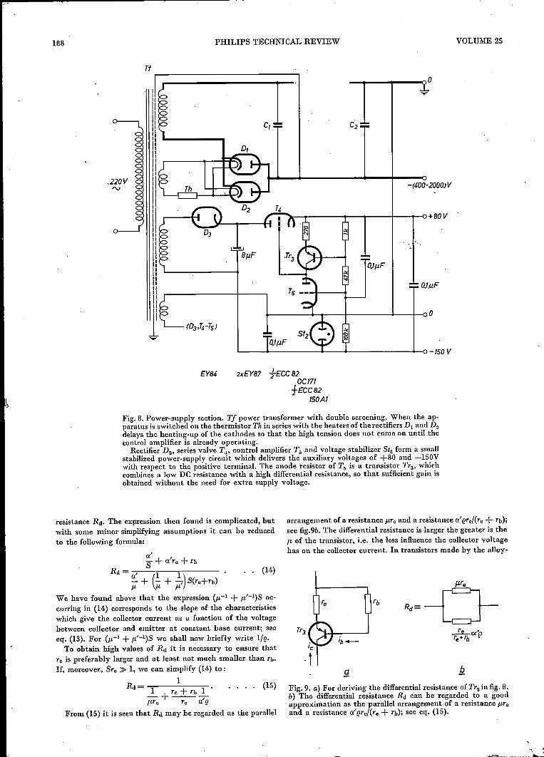
As we have seen, two auxiliary stabilized voltagesources are needed, one ofwhich delivers ~150V andthe other +80V with respect to the positive ter-minal. Both voltages are drawn from one auxiliarystabilized power supply. Here, too, a combination ofa valve and a transistor is used to good advantage.The circuit is shown in jig. 8. One half (T4) of
an ECC 82 double triode is used as the series valveof the auxiliary stabilized power supply, a stabilizertube St2 (type 150 AI) serves as the reference voltagesource, and the other half of the ECC 82 (Ts) servesas the control amplifier. To obtain sufficient gain itis necessary to give Ts a fairly high anode resistance.An ordinary resistor, however, would call for a highsupply voltage. As such only the unregulated DCvoltage is available, but if this were used it wouldconsiderably reduce the stabilization.This difficulty is circumvented by ~mploying a
transistor (Tr 3) as the anode resistor. This can be done
-(400-2000)11
because a transistor with a fixed base voltage and aresistor in series with the emitter (fig. 8) has a veryhigh differential resistance in the collector circuit.The DC resistance ofthe transistor is low, however,so that the stabilized DC voltage can be used (+80Vterminal) for feeding the valve Ts and the transistortogether. The only condition here is that the cathodeof the series valve T4 should be more than 3V positivewith respect to the grid, which is easily ~ulfilled.
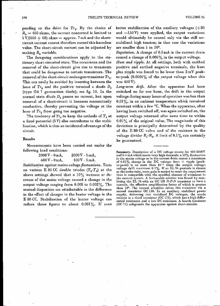
Differetuial. resistance of the transistor in jig. 8The circuit contaiuing the transistor Tra of fig. 8 is shown
in jig. 9a. Using equations (7), (8) and (9) and the relationVb = :'_ibTb, we find for the changes in the collector and basecurrents the following expressions:
From this we can solve vc/ic, which is equal to the required
187
188 PHILIPS TECHNICAL REVIEW
Tf ,---------------------,
VOLUME 25
_ ......._ .....__ -00
2xEY87 fECC 82OCI71
,-tECC82ISOAI
EY84
-(400-2000)V
o,lp.F
Fig. 8. Power-supply section. Tf power transformer with double screening. When the ap-paratus is switched on the thermistor Tit in series with the heaters of therectifiers Dl and D2
delays the heating-up of the cathodes so that the high tension does not come on until thecontrol amplifier is already operating.
Rectifier D3' series valve T4, control amplifier Ts and voltage stabilizer St2 form a smallstabilized power-supply circuit which delivers the auxiliary voltages of +80 and -150Vwith respect to the positive terminal. The anode resistor of Ts is a transistor Tr3, whichcombines a low DC resistance with a high differential resistance, so that sufficient gaiu isobtained without the need for extra supply voltage.
resistance Rd. The expression then found is complicated, butwith some minor simplifying assumptions it can be reducedto the following formula:
a'S+ o'r; + rbRd=
~ + (~ + ~/) S(re+rb)
We have found above that the expression (f-I,-1 + f-1,'-l)S oc-curring in (14) corresponds to the slope of the characteristicswhich give the collector current as a function of the voltagebetween collector and emitter at constant base current; seeeq, (13). For (ft-1 + f-1,'-1)S we shall now briefly write l/e.
To obtain high values of Rd it is necessary to ensure thatre is preferably larger and at least not much smaller than rb·If, moreover, Src» 1, we 'can simplify (14) to:
1Rd= . (15)
1 + Te+ Tb 1f-I,Te --Te- a'e
From (15) it is seen that Rd may be regarded as the parallel
arrangement of a resistance f-I,Teand a resistance a' (!re/(Te+ Tb);
see fig.9b. The differential resistance is larger the greater is theft of the transistor, i.e. the less influence the collector voltagehas on the collector current. In transistors made by the alloy-
(14)
Fig. 9. a) For deriving the differential resistance of Tr3 in fig. 8.b) The differentlal resistance Rd can be regarded to a goodapproximation as the parallel arrangement of a resistance f-I,Teand a resistance a' (!Te/(Te+ Tb); see eq. (15).
1963/64, No. 8 A STABILIZED 2000V POWER SUPPLY 189
diffusion technique ("p.o.b." transistors) 6), such as typeDC 171, this influence is much less than in other transistors,e.g. type DC 71. With an DC 171 transistor, therefore, excep-tionally high differential resistances can be obtained.If re is infinitely large and rb is finite, Rd according to (15)
attains its maximum value, which is equal to a' (!. For theDC171 this limiting value is about 10 MO, for the DC 71about 0.5 MO. As already noted, in the present case a muchlower value of Rd suffices.
Voltage divider
The DC output voltage can be varied by varyingthe resistance R2 of the voltage divider (fig.7). In aparticular case it was :tequi:redthat the voltage shouldbe variable in steps of 200V from 2000V to 400V,and moreover that there should be ten steps of 20Vand ten steps of 2V available. For this purpose R2was built up from seven resistors of 180 kn, ten of18 kn and ten of 1.8 kn; RI consisted of a fixedresistor of 82kn in series with a continuouslyvariablecorrection resistor of 0 to 15 kn. All these resistorsare metallic and their temperature coefficient islower than 5X 10⁻⁵ per "C.
When varying R2 measures are needed to guardagainst switching transients that could endanger thetransistors. This is done by the circuit describedbelow, which offers proteetion against the conse-quences of short-circuiting the output.The transistors could also be damaged if the high
tension came on too quickly after switching on theapparatus. For this reason a thermistor (Th in fig.8),which at room temperature has a 70 times greaterresistance than at the working temperature, isconnected in series with the heaters of the rectifyingvalves (2 EY 87 rectifiers in parallel). This thermistordelays the heating of the cathodes to such an extentthat the high tension does not come on until thecontrol amplifier is already in operation.
Proteetion. against the consequences of short-circuitingof the output
It is particularly useful for power-supply ap-paratus - especially if intended for experimentalpurposes - to be proof against short-circuiting. Itproved possible to give this property to the DC volt-age source described here by the addition of only onetransistor, one diode and a few resistors.A short-circuited output presents two dangers:
1) During a short-circuit the voltage between thecathode and control grid of the EL 34 can riseabove 20 V, thereby exceeding the permissiblevalue for the transistor TrI'
6) P.J.W. Jochems, The alloy-diffusion technique for manu-facturing high-frequency transistors, Philips tech. Rev.24,231-239, 1962/63 (No. 8).
I)
2) The direct current becomes so high that variouscomponents are overloaded.
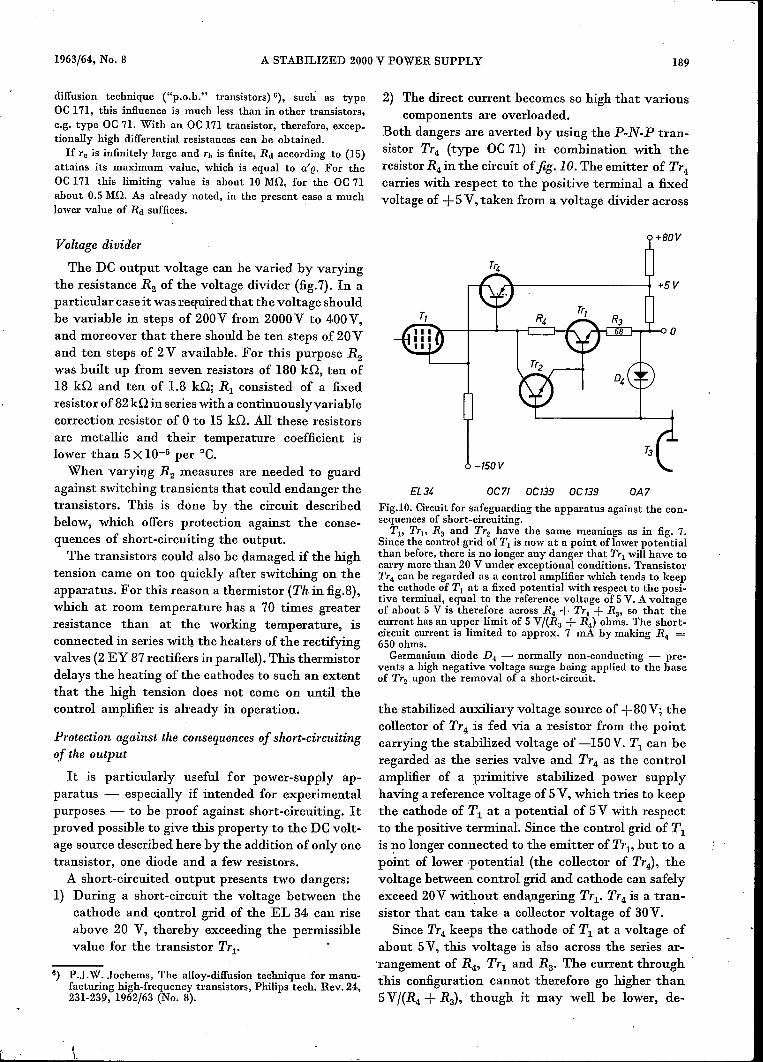
Both dangers are averted by using the P-N-P tran-sistor Tr4 (type OC 71) in combination with theresistor R4 in the circuit of fig. 10. The emitter of Tr 4carries with respect to the positive terminal a fixedvoltage of +5 V, taken from a voltage divider across
T,
Tr;.
-ISO V
£L34 oe 71 oe 139 oe 139 OA7Fig.l0. Circuit for safeguarding the apparatus against the con-sequences of short-circuiting.
Tl' TrI' R3 and Tr2 have the same meanings as in fig. 7.Since the control grid of Tl is now at a point of lower potentialthan before, there is no longer any danger that TrI will have tocarry more than 20 V under exceptional conditions. TransistorTr4 can he regarded as a control amplifier which tends to keepthe cathode of Tl at a fixed potential with respect to the posi-tive terminal, equal to the reference voltage of 5V. A voltageof about 5 V is therefore across R4 + TrI + R3' so that thecurrent has an upper limit of 5V/(R3 + R4) ohms. The short-circuit current is limited to approx. 7 mA by making R4 =650 ohms.Germanium diode D4 - normally non-conducting - pre-
vents a high negative voltage surge being applied to the baseof Tr2 upon the removal of a short-circuit.
the stabilized auxiliary voltage source of +80V; thecollector of Tr4 is fed via a resistor from the pointcarrying the stabilized voltage of -150V. Tl can beregarded as the series valve and Tr 4 as the controlamplifier of a primitive stabilized power supplyhaving a reference voltage of 5V, which tries to keepthe cathode of Tl at a potentialof 5V with respectto the positive terminal. Since the control grid of Tlis ~o longer connected to the emitter of TrI' but to apoint of lower -potential (the collector of Tr4), thevoltage between control grid and cathode can safelyexceed 20V without endangering TrI' Tr4 is a tran-sistor that can take a collector voltage of 30V.
Since Tr4 keeps the cathode of Tl at a voltage ofabout 5V, this voltage is also across the series ar-'rangement of R4> TrI and Ra. The current throughthis configuration cannot therefore go higher than5Vj(R4 + Ra), though it may well be lower, de-
190 PHILlPS TECHNICAL REVIEW VOLUME 25
pending on the drive for Trl• By the choice ofR4 = 650 ohms, the current concerned is limited to5V/(650 + 68) ohms = approx. 7mA and the short-circuit current cannot therefore exceed this harmlessvalue. The short-circuit current ean be adjusted bymaking R4 variable.
The foregoing considerations apply. to the st~-tionary short-circuited state. The occurrence and theremoval of the short-circuit give rise to transientsthat could be dangerous t? certain transistors. Theremoval ofthe short-circuit endangers transistor Tr2•This can easily be avoided by inserting between thebase of Tr2 and the positive terminal a diode D4(type OA 7 germanium diode); see fig. 10. In thenormal state diode P4 passes no current, but uponremoval of a short-circuit it becomes momentarilyconductive, thereby preventing the voltage at thebase of Tr2 from going too negative. .
The tendency of Tr4 to keep the cathode of Tl ata fixed potential (5V) also contributes to the stabi-lization, which is thus an incidental advantage of thecircuit.
Results
Measurements have been carried out under thefollowing load conditions:
2000V - OmA, 2000V - 5mA,400V - OmA, 400V - 5mA.
Stabiliztuion. against mains-voltage flucuuuions. Testson various E 80 CC double triodes (T2-Ta) at theabove settings showed that a 10% increase or de-crease of the mains voltage caused a change in theoutput voltage ranging from 0.008 to 0.002%. Themutual disparities are attributable to the differencein the effect of changes in the heater voltage in theE 80 CC. Stabilization of the heater voltage canreduce these figures to about 0.001%. If even
better stabilization of the auxiliary voltages (+80and -150V) were applied, the output variationswould ultimately be caused only via the still un-stabilized high tension; in that case the variationsare smaller than 1 in 106•Regulation. A change of 0.5mA in the current drain.caused a change of 0.005% in the output voltage.Hum and ripple. At all settings, both with earthedpositive and earthed negative terminals, the humplus ripple was found to be lower than 2mV peak-to-peak (0.0005% of the ,output voltage when thiswas 400V).Long-term drift. After the apparatus had beenswitched on for one hour, the drift in the outputvoltage during many hours of operation was less than0.,01%, in an ambient temperature which remainedconstant within a few °C. Wll@ the apparatus, afterhaving be~n switched off, was again switched on, theoutput voltage returned after some time to within0.01% of the original value. The magnitude of thisdeviation is principally determined by the qualityof the E 80 CC valve and of the resistors in thevoltage divider RI-R2. A limit of 0.1% can certainlybe guaranteed.
Summary. Description of a DC voltage source for 400-2000Vand 0-5 mAwhichmeets very high demands: a 10% fluctuationin the mains voltage or in the current drain causes a maximumof 0.01% change in the DC voltage; hum + ripple (peak-to-peak) is no more than 10-5 times the output voltage;voltage drift maximum 0_1%. If an EL 34 pentode is chosenas the series tube, more gain is needed to meet the requirementthan is compatible with the specifiedabsence of overshoot inthe control system. A favourable solution was found by com-bining the EL 34 with an DC 139 N-P-N transistor to form acascode, the effective amplification factor of which is greaterthan 105. The control amplifier drives this transistor via asecond transistor DC139. In an auxiliary stabilized powersupply, delivering two stabilized DC voltages, the anoderesistor is a third transistor (DC171),which has a high differ-ential resistance and a low DC resistance. A fourth transistor(DC71) safeguards the apparatus against short-circuits.